si32260-61 data sheet - silicon labs
TRANSCRIPT

Skyworks Solutions, Inc. • Phone [781] 376-3000 • Fax [781] 376-3100 • [email protected] • www.skyworksinc.comRev. 1.4 • Skyworks Proprietary Information • Products and Product Information are Subject to Change Without Notice • October 7, 2021
Si32260/1
SINGLE-CHIP DUAL PROSLIC®
Si32260/1 Features
Applications
Description
The Si32260/1 Dual ProSLIC® devices, in a single package, implementtwo complete foreign exchange station (FXS) telephony interfaces. TheSi32260/1 devices operate from a 3.3 V supply and have standardPCM/SPI or GCI (8x8 mm package only) bus digital interfaces. A pair ofbuilt-in dc-dc converter controllers can be used to automatically generatethe optimal battery voltage required for each line-state, optimizingefficiency and minimizing heat generation.
The Si32260/1 devices are designed to operate not only with a trackingbattery supply for each channel for lowest power consumption, but alsowith shared battery supplies, for lowest cost. When used with sharedbattery supplies, the internal dc-dc controller operates in Tracking SharedSupply (TSS) mode to deliver power consumption lower than typical fixedvoltage shared rail designs (shared supplies are not currently supportedby the 6 x 8 mm package option).
Self-testing and metallic loop testing (MLT) (e.g., GR-909) is facilitated bythe built-in DSP, monitor ADC, and test load. The devices are availablewith linefeed voltage ratings of –110 V (Si32260) or –140 V (Si32261) tosupport high voltage ringing, and both devices support wideband audiofor better-than-PSTN voice quality. The Si32260/1 devices are availablein a 6 x 8 mm 47-pin QFN package or an 8 x 8 mm 60-pin QFN package.
Two complete FXS channels in a single 6 x 8 mm or 8 x 8 mm package
Performs all BORSCHT functions Ideal for short- or long-loop applications Ultra low power consumption Internal balanced or unbalanced ringing Patented low power ringing Adaptive ringing Simplified configuration and diagnostics
Supported by ProSLIC APIGR-909 loop diagnosticsAudio diagnostics with loopbackIntegrated test load
Wideband voice support On-hook transmission Loop or ground start operation Smooth polarity reversal Pulse metering PCM and SPI bus digital interfaces with
programmable interrupts
Software-programmable parameters:Ringing frequency, amplitude,
cadence, and waveshapeTwo-wire ac impedanceTranshybrid balanceDC current loop feed (10–45 mA)Loop closure and ring trip thresholdsGround key detect threshold
Integrated dc-dc controllers with direct connection to MOSFET
Three high voltage supply optionsFull trackingTracking shared suppliesFixed rail
DTMF generator/decoder A-Law/µ-Law companding, linear PCM GCI/IOM-2 mode support 3.3 V operation Pb-free/RoHS-compliant packaging
VoIP gateways and routers xDSL IADs Optical Network Terminals/Units (ONT/U) Analog Terminal Adapters (ATA) Cable eMTA
Wireless Fixed Terminals (WFT) Wireless Local Loop (WLL) WiMAX CPE Private Branch Exchange (PBX) VoIP MDU gateways
Patents pending
Ordering Information
See page 45.
Pin Assignments
Si32260/1 8x8 mm
1
2
3
4
5
6
7
8
9
10
11
12
13
14
15
16
17
18
19 20 21 22 23 24 25 26 27 28 29 30 31
32
33
34
35
36
37
38
39
40
41
42
43
44
45
46474849505152
5354555657
585960TIPa
N/C
GPIO2A / SRINGCa
GPIO1a / STIPCa
SRINGDCa
SRINGACa
STIPACa
STIPDCa
CAPPa
CAPMa
SVBATa
SVDC
RSTB
INTB / DTXENB
FSYNC
SD
ITH
RU
PC
LK
DA
TA
o
DA
TA
i
SD
CH
a
SD
CL
a
DC
DR
Va
AU
Xoi
AU
Xd
rv
DC
DR
Vb
SD
CL
b
SD
CH
b
VD
DD
VD
DR
EG
CS
B
SC
LK
SDO
SDI
SVBATb
CAPMb
CAPPb
IREF
STIPDCb
STIPACb
SRINGACb
SRINGDCb
GPIO1b / STIPCb
GPIO2b / SRINGCb
VDDA
N/C
TIPb
N/C
RIN
Gb
VB
AT
b
N/C
BA
SE
b
N/C
N/C
N/C
N/C
N/C
BA
T_
PO
BA
SE
a
VB
AT
a
RIN
Ga
HVPAD
GND PAD
Si32260/1 6x8 mm
1
2
3
4
5
6
7
8
9
10
11
12
13
14
15
16
HVPAD
GNDPAD
TIP
a
TIP
b
RIN
Gb
VB
AT
b
VB
AT
a
RIN
Ga
GPIO1a / STIPCa
SRINGDCa
SRINGACa
STIPACa
STIPDCa
CAPPa
CAPMa
SVBATa
SVDC
RSTB
INTB / DTXENB
FSYNC
PCLK
DTX
GPIO2A / SRINGCa
DRX
SD
CH
a
SD
CLa
DC
DR
Va
DC
FF
a
DC
FF
b
DC
DR
Vb
SD
CL
b
SD
CH
b
VD
DD
28
31
26
27
29
30
32
33
34
35
36
37
38
39
40
41
2524232221201917 18
4647 45 44 43 42
VDDREG
CSB
SCLK
SDO
SDI
SVBATb
CAPMb
CAPPb
IREF
STIPDCb
STIPACb
SRINGACb
SRINGDCb
GPIO1b / STIPCb
GPIO2b / SRINGCb
VDDA

Si32260/1
2 Skyworks Solutions, Inc. • Phone [781] 376-3000 • Fax [781] 376-3100 • [email protected] • www.skyworksinc.comRev. 1.4 • Skyworks Proprietary Information • Products and Product Information are Subject to Change Without Notice • October 7, 2021
Functional Block Diagram
SPIControl
Interface
PCM/GCI
Interface
DSP
DTMF &Tone Gen
Pro
gram
ma
ble
AC
Impe
danc
ean
d H
ybrid
Caller ID
RingingGenerator
ADC
DAC
CODEC SLICLinefeedControl
LinefeedMonitor
DC-DC Controller
Line Diagnostics
PLLPCLK
FSYNC
DRX
DTX
CS
SDI
SDO
SCLK
INT
RST
SPIControl
Interface
PCM/GCI
Interface
DSP
DTMF &Tone Gen
Pro
gram
mab
le
AC
Im
peda
nce
and
Hyb
rid
Caller ID
RingingGenerator
ADC
DAC
CODEC
DC-DC Controllers
Line Diagnostics
PLLPCLK
FSYNC
DRX
DTX
CS
SDI
SDO
SCLK
INT
RST
Si32260/1
DACRING
TIP
Line
feed
Channel A
CODEC SLIC
DACRING
TIP
Line
feed
Channel B
CODEC SLIC
ADC
ADC
LinefeedControl
LinefeedMonitor
LinefeedControl
LinefeedMonitor

Si32260/1
Skyworks Solutions, Inc. • Phone [781] 376-3000 • Fax [781] 376-3100 • [email protected] • www.skyworksinc.com 3Rev. 1.4 • Skyworks Proprietary Information • Products and Product Information are Subject to Change Without Notice • October 7, 2021
TABLE OF CONTENTS
Section Page
1. Electrical Specifications . . . . . . . . . . . . . . . . . . . . . . . . . . . . . . . . . . . . . . . . . . . . . . . . . . .52. Typical Application Circuits . . . . . . . . . . . . . . . . . . . . . . . . . . . . . . . . . . . . . . . . . . . . . . .20
2.1. Flyback Tracking DC-DC Converter . . . . . . . . . . . . . . . . . . . . . . . . . . . . . . . . . . . . .202.2. Low Cost Quasi Ćuk (LCQC) . . . . . . . . . . . . . . . . . . . . . . . . . . . . . . . . . . . . . . . . . .23
3. Bill of Materials . . . . . . . . . . . . . . . . . . . . . . . . . . . . . . . . . . . . . . . . . . . . . . . . . . . . . . . . . .264. Functional Description . . . . . . . . . . . . . . . . . . . . . . . . . . . . . . . . . . . . . . . . . . . . . . . . . . .305. FXS Features . . . . . . . . . . . . . . . . . . . . . . . . . . . . . . . . . . . . . . . . . . . . . . . . . . . . . . . . . . .31
5.1. DC Feed Characteristics . . . . . . . . . . . . . . . . . . . . . . . . . . . . . . . . . . . . . . . . . . . . . .315.2. Linefeed Operating States . . . . . . . . . . . . . . . . . . . . . . . . . . . . . . . . . . . . . . . . . . . .315.3. Line Voltage and Current Monitoring . . . . . . . . . . . . . . . . . . . . . . . . . . . . . . . . . . . .315.4. Power Monitoring and Power Fault Detection . . . . . . . . . . . . . . . . . . . . . . . . . . . . . .315.5. Thermal Overload Shutdown . . . . . . . . . . . . . . . . . . . . . . . . . . . . . . . . . . . . . . . . . .315.6. Loop Closure Detection . . . . . . . . . . . . . . . . . . . . . . . . . . . . . . . . . . . . . . . . . . . . . . .335.7. Ground Key Detection . . . . . . . . . . . . . . . . . . . . . . . . . . . . . . . . . . . . . . . . . . . . . . . .335.8. Ringing Generation . . . . . . . . . . . . . . . . . . . . . . . . . . . . . . . . . . . . . . . . . . . . . . . . . .335.9. Polarity Reversal . . . . . . . . . . . . . . . . . . . . . . . . . . . . . . . . . . . . . . . . . . . . . . . . . . . .355.10. Two-Wire Impedance Synthesis . . . . . . . . . . . . . . . . . . . . . . . . . . . . . . . . . . . . . . .355.11. Transhybrid Balance Filter . . . . . . . . . . . . . . . . . . . . . . . . . . . . . . . . . . . . . . . . . . .355.12. Tone Generators . . . . . . . . . . . . . . . . . . . . . . . . . . . . . . . . . . . . . . . . . . . . . . . . . . .355.13. DTMF Detection . . . . . . . . . . . . . . . . . . . . . . . . . . . . . . . . . . . . . . . . . . . . . . . . . . .355.14. Pulse Metering . . . . . . . . . . . . . . . . . . . . . . . . . . . . . . . . . . . . . . . . . . . . . . . . . . . .355.15. DC-DC Controller . . . . . . . . . . . . . . . . . . . . . . . . . . . . . . . . . . . . . . . . . . . . . . . . . .355.16. Wideband Audio . . . . . . . . . . . . . . . . . . . . . . . . . . . . . . . . . . . . . . . . . . . . . . . . . . .355.17. In-Circuit and Metallic Loop Testing (MLT) . . . . . . . . . . . . . . . . . . . . . . . . . . . . . .36
6. System Interfaces . . . . . . . . . . . . . . . . . . . . . . . . . . . . . . . . . . . . . . . . . . . . . . . . . . . . . . . .376.1. SPI Control Interface . . . . . . . . . . . . . . . . . . . . . . . . . . . . . . . . . . . . . . . . . . . . . . . . .376.2. PCM Interface and Companding . . . . . . . . . . . . . . . . . . . . . . . . . . . . . . . . . . . . . . . .37
7. Pin Descriptions: Si32260/1 . . . . . . . . . . . . . . . . . . . . . . . . . . . . . . . . . . . . . . . . . . . . . . .387.1. Si32260/61 6x8 mm Package . . . . . . . . . . . . . . . . . . . . . . . . . . . . . . . . . . . . . . . . . .387.2. Si32260/61 8x8 mm Package . . . . . . . . . . . . . . . . . . . . . . . . . . . . . . . . . . . . . . . . . .41
8. Ordering Guide . . . . . . . . . . . . . . . . . . . . . . . . . . . . . . . . . . . . . . . . . . . . . . . . . . . . . . . . . .459. Product Identification . . . . . . . . . . . . . . . . . . . . . . . . . . . . . . . . . . . . . . . . . . . . . . . . . . . .4710. Package Outlines . . . . . . . . . . . . . . . . . . . . . . . . . . . . . . . . . . . . . . . . . . . . . . . . . . . . . . .48
10.1. 47-Pin QFN/LGA (6x8 mm) . . . . . . . . . . . . . . . . . . . . . . . . . . . . . . . . . . . . . . . . . . .4810.2. 60-Pin QFN/LGA (8x8 mm) . . . . . . . . . . . . . . . . . . . . . . . . . . . . . . . . . . . . . . . . . . .4910.3. 60-Pin QFN (8x8 mm) . . . . . . . . . . . . . . . . . . . . . . . . . . . . . . . . . . . . . . . . . . . . . . .50
11. PCB Land Pattern—LGA Package . . . . . . . . . . . . . . . . . . . . . . . . . . . . . . . . . . . . . . . . .5111.1. Land Pattern and Solder Mask Design–QFN-47 (6x8 mm) . . . . . . . . . . . . . . . . . .5111.2. Land Pattern and Solder Mask Design–QFN-60 (8x8 mm) . . . . . . . . . . . . . . . . . .5211.3. Thermal via Layout–QFN-47 (6x8 mm) . . . . . . . . . . . . . . . . . . . . . . . . . . . . . . . . . .5311.4. Thermal via Layout–QFN-60 (8x8 mm) . . . . . . . . . . . . . . . . . . . . . . . . . . . . . . . . . .53

Si32260/1
4 Skyworks Solutions, Inc. • Phone [781] 376-3000 • Fax [781] 376-3100 • [email protected] • www.skyworksinc.comRev. 1.4 • Skyworks Proprietary Information • Products and Product Information are Subject to Change Without Notice • October 7, 2021
11.5. Stencil Aperture Design–QFN-47 (6x8 mm) . . . . . . . . . . . . . . . . . . . . . . . . . . . . . .5411.6. Stencil Aperture Design–QFN-60 (8x8 mm) . . . . . . . . . . . . . . . . . . . . . . . . . . . . . .55
12. Top Markings . . . . . . . . . . . . . . . . . . . . . . . . . . . . . . . . . . . . . . . . . . . . . . . . . . . . . . . . . .5612.1. Top Marking (47-Pin LGA) . . . . . . . . . . . . . . . . . . . . . . . . . . . . . . . . . . . . . . . . . . .5612.2. Top Marking Explanation (47-pin LGA) . . . . . . . . . . . . . . . . . . . . . . . . . . . . . . . . . .5612.3. Top Marking (60-Pin LGA) . . . . . . . . . . . . . . . . . . . . . . . . . . . . . . . . . . . . . . . . . . .5712.4. Top Marking Explanation (60-Pin LGA) . . . . . . . . . . . . . . . . . . . . . . . . . . . . . . . . .57
13. Si3226x Support Documentation . . . . . . . . . . . . . . . . . . . . . . . . . . . . . . . . . . . . . . . . . .57Document Change List: . . . . . . . . . . . . . . . . . . . . . . . . . . . . . . . . . . . . . . . . . . . . . . . . . . . . .58

Si32260/1
Skyworks Solutions, Inc. • Phone [781] 376-3000 • Fax [781] 376-3100 • [email protected] • www.skyworksinc.com 5Rev. 1.4 • Skyworks Proprietary Information • Products and Product Information are Subject to Change Without Notice • October 7, 2021
1. Electrical Specifications
Table 1. Recommended Operating Conditions1
Parameter Symbol Test Condition Min Typ Max Unit
Ambient Temperature TA
F-grade 0 25 70 °C
G-grade –40 25 85 °C
Silicon Junction Temperature, QFN-60, QFN-47
TJHV Linefeed Die — — 1452 °C
Supply Voltage, Si32260/1 VDDD, VDDA 3.13 3.3 3.47 V
Battery Voltage, Si322603 VBAT –110 — –15 V
Battery Voltage, Si322613 VBAT –140 — –15 V
Notes:1. All minimum and maximum specifications apply across the recommended operating conditions. Typical values apply at
nominal supply voltages and an operating temperature of 25 °C unless otherwise stated.2. Except during ringing.3. Operation at minimum voltage dependent upon loop conditions and dc-dc converter configuration.
Table 2. AC Characteristics
Parameter Test Condition Min Typ Max Unit
TX/RX Performance
Overload Compression 2-Wire – PCM Figure 5 — —
Single Frequency Distortion(0 dBm0 input)
0 Hz to 4 kHz — — –40 dBm0
0 Hz – 12 kHz — — –28 dBm0
Signal-to-(Noise + Distortion) Ratio1
200 Hz to 3.4 kHzD/A or A/D 8-bit
Active off-hook, and OHT, any ZT
Figure 4 — —
Audio Tone Generator Signal-to-Distortion Ratio1
0 dBm0, Active off-hook, and OHT, any ZT
46 — — dB
Intermodulation Distortion — — –41 dB
Gain Accuracy1 2-Wire to PCM or PCM to 2-Wire1014 Hz, any gain setting
–0.2 — 0.2 dB
Attenuation Distortion vs. Freq. 0 dBm05 See Figure 6 and 7
Notes:1. Analog signal measured as VTIP – VRING. Assumes ideal line impedance matching.2. The quantization errors inherent in the µ/A-law companding process can generate slightly worse gain tracking
performance in the signal range of 3 to –37 dB for signal frequencies that are integer divisors of the 8 kHz PCM sampling rate.
3. VDDD, VDDA = 3.3 V, VBAT = –52 V, no fuse resistors; RL = 600 , ZS = 600 synthesized using RS register coefficients.
4. The level of any unwanted tones within the bandwidth of 0 to 4 kHz does not exceed –55 dBm.5. 0 dBm0 is equal to 0 dBm into 600 .

Si32260/1
6 Skyworks Solutions, Inc. • Phone [781] 376-3000 • Fax [781] 376-3100 • [email protected] • www.skyworksinc.comRev. 1.4 • Skyworks Proprietary Information • Products and Product Information are Subject to Change Without Notice • October 7, 2021
Group Delay vs. Frequency See Figure 8 and 9
Gain Tracking2 1014 Hz sine wave, reference level –10 dBm
Signal level:
3 dB to –37 dB — — 0.25 dB
–37 dB to –50 dB — — 0.5 dB
–50 dB to –60 dB — — 1.0 dB
Round-Trip Group Delay 1014 Hz, Within same time-slot — 450 500 µs
2-Wire Return Loss3 200 Hz to 3.4 kHz 26 30 — dB
Transhybrid Balance3 300 Hz to 3.4 kHz 26 30 — dB
Noise Performance
Idle Channel Noise4 C-Message weighted — 8 12 dBrnC
Psophometric weighted — –82 –78 dBmP
PSRR from VDDD, VDDA @ 3.3 V RX and TX, 200 Hz to 3.4 kHz — 55 — dB
Longitudinal Performance
Longitudinal to Metallic/PCM Balance (forward or reverse)
200 Hz to 1 kHz 58 60 — dB
1 kHz to 3.4 kHz 53 58 — dB
Metallic/PCM to Longitudinal Balance
200 Hz to 3.4 kHz 40 — — dB
Longitudinal Impedance 200 Hz to 3.4 kHz at TIP or RING — 50 —
Longitudinal Current Capability Active off-hook 60 Hz Reg 73 = 0x0B
— 25 — mA
Table 2. AC Characteristics (Continued)
Parameter Test Condition Min Typ Max Unit
Notes:1. Analog signal measured as VTIP – VRING. Assumes ideal line impedance matching.2. The quantization errors inherent in the µ/A-law companding process can generate slightly worse gain tracking
performance in the signal range of 3 to –37 dB for signal frequencies that are integer divisors of the 8 kHz PCM sampling rate.
3. VDDD, VDDA = 3.3 V, VBAT = –52 V, no fuse resistors; RL = 600 , ZS = 600 synthesized using RS register coefficients.
4. The level of any unwanted tones within the bandwidth of 0 to 4 kHz does not exceed –55 dBm.5. 0 dBm0 is equal to 0 dBm into 600 .

Si32260/1
Skyworks Solutions, Inc. • Phone [781] 376-3000 • Fax [781] 376-3100 • [email protected] • www.skyworksinc.com 7Rev. 1.4 • Skyworks Proprietary Information • Products and Product Information are Subject to Change Without Notice • October 7, 2021
Table 3. Power Supply Characteristics
Parameter Symbol Test Condition Min Typ Max Unit
Supply currents: Reset
IDD VT and VR = Hi-Z , RST = 0 — 3.5 — mA
IVBAT — 0 — mA
Supply currents:High Impedance, Open
IDD VT and VR = Hi-Z — 23 — mA
IVBAT — 0.6 — mA
Supply currents:Forward/Reverse, On-hook
IDDVTR = –48 V,
Automatic Power Save Mode enabled
— 10 — mA
IVBAT — 0.4 — mA
Supply currents:Forward/Reverse, On-hook
IDDVTR = –48 V,
Automatic Power Save Mode disabled
— 35 — mA
IVBAT — 2.2 — mA
Supply currents:Tip/Ring Open, On-hook
IDDVT or VR = –48 V VR or VT = Hi-Z,
Automatic Power Save Mode enabled
— 10 — mA
IVBAT — 0.4 — mA
Supply currents:Tip/Ring Open, On-hook
IDDVT or VR = –48 V VR or VT = Hi-Z,
Automatic Power Save Mode enabled
— 35 — mA
IVBAT — 1.5 — mA
Supply currents:Forward/Reverse OHT, On-hook
IDDVTR = 48 V — 53 — mA
IVBAT — 3 — mA
Supply currents:Forward/Reverse Active, Off-hook
IDDILOOP = 20 mA RLOAD = 200 Ω — 54 — mA
IVBAT — 2.2 + ILOOP
— mA
Supply currents:Ringing
IDDVTR =55VRMS + 0 VDC,
balanced, sinusoidal, f = 20 Hz, RLOAD = 5 REN = 1400
— 40 — mA
IVBAT — 38 — mA
Notes:1. All specifications are for a single channel of Si3226x with a tracking flyback dc-dc converter, when both channels are
in the same operating state.2. ILOOP is the dc current in the subscriber loop during the off-hook state.

Si32260/1
8 Skyworks Solutions, Inc. • Phone [781] 376-3000 • Fax [781] 376-3100 • [email protected] • www.skyworksinc.comRev. 1.4 • Skyworks Proprietary Information • Products and Product Information are Subject to Change Without Notice • October 7, 2021
Table 4. Linefeed Characteristics
Parameter Symbol Test Condition Min Typ Max Unit
Maximum Loop Resistance RLOOP
RDC,MAX = 430 ILOOP = 18 mA, VBAT = –52 V,
RPROT = 0 — — 2000
DC Feed Current
Differential — — 45 mA
Common Mode — — 30 mA
Differential + Common Mode — — 45 mA
DC Loop Current Accuracy ILIM = 18 mA — — 10 %
DC Open Circuit Voltage Accuracy
Active Mode; VOC = 48 V, VTIP – VRING
— — 4 V
DC Differential OutputResistance
RDO ILOOP < ILIM 160 — 640
DC On-Hook VoltageAccuracy—Ground Start
VOHTOIRING<ILIM; VRING wrt ground,
VRING = –51 V— — 4 V
DC OutputResistance—Ground Start
RROTO IRING<ILIM; RING to ground 160 — 640
DC Output Resistance—Ground Start
RTOTO TIP to ground 400 — — k
Loop Closure DetectThreshold Accuracy
ITHR = 13 mA — — 10 %
Ground Key DetectThreshold Accuracy
ITHR = 13 mA — — 10 %
Ring TripThreshold Accuracy
AC detection,VRING = 70 Vpk, no offset,
ITH = 80mA— — 4 mA
DC detection,20 V dc offset, ITH = 13 mA
— — 1 mA
DC Detection,48 V DC offset, Rloop = 1500 — — 3 mA
Ringing Amplitude* VRINGING
Si32260 Open circuit, VBAT = –110 V
— –108 — VPK
Si32261 Open circuit, VBAT = –140 V
— –136 — VPK
Sinusoidal Ringing Total Harmonic Distortion
RTHD
Si32260 : 60 VRMS, 15 VOFFSET, 0–5 REN
— 1 — %Si32261 : 55 VRMS,
48 VOFFSET, 0–5 REN
Ringing Frequency Accuracy f = 16 Hz to 60 Hz — — 1 %
*Note: Ringing amplitude is set for 108 or 128 V peak and measured at TIP-RING using no series protection resistance.

Si32260/1
Skyworks Solutions, Inc. • Phone [781] 376-3000 • Fax [781] 376-3100 • [email protected] • www.skyworksinc.com 9Rev. 1.4 • Skyworks Proprietary Information • Products and Product Information are Subject to Change Without Notice • October 7, 2021
Ringing Cadence Accuracy Accuracy of ON/OFF times — — 50 ms
Loop Voltage Sense Accuracy
VTIP – VRING = 48 V — 2 4 %
Loop CurrentSense Accuracy
ILOOP = 18 mA — 7 10 %
Power AlarmThreshold Accuracy
Power Threshold = 1.0 WVBAT = –56 V, ILDDD = 40 mA,
RLOAD = 600 — 15 — %
Test Load Impedance RTESTHVIC_STATE_SPARE[23] = 1;
VT/R 50 V1.0 — 3.0 k
Test Load Voltage VTL HVIC_STATE_SPARE[23] = 1 ±5 ±50 V
Table 5. Digital I/O Characteristics
Parameter Symbol Test Condition Min Typ Max Unit
High Level Input Voltage VIH 2.0 — VDD V
Low Level Input Voltage VIL 0 — 0.8 V
High Level Output Voltage
VOH
DTX, SDO, SDITHRU,GPIO1/STIPC, GPIO2/SRINGC:
IO = –4 mAVDD – 0.6 — — V
Low Level Output Voltage
VOL
DTX, SDO, INT,SDITHRU,
GPIO1/STIPC, GPIO2/SRINGC:IO = 4 mA
— — 0.4 V
SDITHRU and RST Internal Pullup Current
33 42 80 µA
Input Leakage Current IL — — 10 µA
Table 4. Linefeed Characteristics (Continued)
Parameter Symbol Test Condition Min Typ Max Unit
*Note: Ringing amplitude is set for 108 or 128 V peak and measured at TIP-RING using no series protection resistance.

Si32260/1
10 Skyworks Solutions, Inc. • Phone [781] 376-3000 • Fax [781] 376-3100 • [email protected] • www.skyworksinc.comRev. 1.4 • Skyworks Proprietary Information • Products and Product Information are Subject to Change Without Notice • October 7, 2021
Figure 1. Reset Timing Diagram
Table 6. Charge Pump Characteristics
Parameter Symbol Test Condition Min Typ Max Unit
Output Voltage (DCDRVa/b, DCFFa/b)
VCP 2 x VDD – 1 — 2xVDD V
Output Current ICP — — 3* mA
*Note: Peak drive current capability is >60 mA.
Table 7. Switching Characteristics—General Inputs*
Parameter Symbol Min Typ Max Unit
RST Pulse Width trl 33/PCLK — — µs
*Note: All timing is referenced to the 50% level of the waveform. Input test levels areVIH = VDD – 0.4 V, VIL = 0.4 V. Rise and Fall times are referenced to the 20% and 80% levels of the waveform.
PCLK
RSTB
31 30 29 28 5 4 3 2 1 1 2 3 4 50 28 29 30 31Counting of PCLKRising Edges
Note: The count of PCLK rising edges during reset will be skewed by 1-2 clocks based on the internal sampling of reset.

Si32260/1
Skyworks Solutions, Inc. • Phone [781] 376-3000 • Fax [781] 376-3100 • [email protected] • www.skyworksinc.com 11Rev. 1.4 • Skyworks Proprietary Information • Products and Product Information are Subject to Change Without Notice • October 7, 2021
Figure 2. SPI Timing Diagram
Table 8. Switching Characteristics—SPI
Parameter Symbol Test Condition Min Typ Max Unit
Cycle Time SCLK tc 62 — — ns
Rise Time, SCLK tr — — 25 ns
Fall Time, SCLK tf — — 25 ns
Delay Time, SCLK Fall to SDO Active td1 — — 20 ns
Delay Time, SCLK Fall to SDO Transition
td2 — — 20 ns
Delay Time, CSB Rise to SDO Tristate td3 — — 20 ns
Setup Time, CSB to SCLK Fall tsu1 25 — — ns
Hold Time, CSB to SCLK Rise th1 20 — — ns
Setup Time, SDI to SCLK Rise tsu2 25 — — ns
Hold Time, SDI to SCLK Rise th2 20 — — ns
Delay Time between Chip Selects tcs 220 — — ns
SDI to SDITHRU Propagation Delay td4 — 4 10 ns
Notes:1. All timing is referenced to the 50% level of the waveform. Input test levels are VIH = VDDD –0.4 V, VIL = 0.4 V.2. Characteristics for outputs specified with CL = 20 pF.
SCLK
CSB
SDI
th1
td3
SDO
td1 td2
tsu1
tr tf
tsu2 th2
tcs
tc
SDITHRU
td4

Si32260/1
12 Skyworks Solutions, Inc. • Phone [781] 376-3000 • Fax [781] 376-3100 • [email protected] • www.skyworksinc.comRev. 1.4 • Skyworks Proprietary Information • Products and Product Information are Subject to Change Without Notice • October 7, 2021
Table 9. Switching Characteristics—PCM Highway Interface1
Parameter Symbol Test Condition
Min2 Typ2 Max2 Unit
PCLK Period tp 122 — 1953 ns
PCLK Jitter Tolerance tjitter 8 nsRMS
Valid PCLK Inputs3
————————
512768
1.0241.5361.5442.0484.0968.192
————————
kHzkHzMHzMHzMHzMHzMHzMHz
FSYNC Period4 tfs — 125 — µs
PCLK Duty Cycle Tolerance tdty 40 50 60 %
FSYNC Jitter Tolerance5 tjitter — — ±120 ns
Rise Time, PCLK tr — — 25 ns
Fall Time, PCLK tf — — 25 ns
Delay Time, PCLK Rise to DTX Active td1 — — 20 ns
Delay Time, PCLK Rise to DTX Transition
td2 — — 20 ns
Delay Time, PCLK Rise to DTX Tri-state6
td3 — — 20 ns
Setup Time, FSYNC to PCLK Fall tsu1 25 — — ns
Hold Time, FSYNC to PCLK Fall th1 20 — — ns
Setup Time, DRX to PCLK Fall tsu2 25 — — ns
Hold Time, DRX to PCLK Fall th2 20 — — ns
FSYNC Pulse Width twfs tp — 125 µs–tp
Notes:1. Characteristics for outputs specified with CL = 20 pF.2. All timing is referenced to the 50% level of the waveform. Input test levels are VIH – VI/O – 0.4 V, VIL = 0.4 V.3. A constant PCLK and FSYNC are required.4. FSYNC source is assumed to be 8 kHz under all operating conditions.5. FSYNC Jitter Tolerance relative to PCLK.6. Specification applies to PCLK fall to DTX tristate when that mode is selected.

Si32260/1
Skyworks Solutions, Inc. • Phone [781] 376-3000 • Fax [781] 376-3100 • [email protected] • www.skyworksinc.com 13Rev. 1.4 • Skyworks Proprietary Information • Products and Product Information are Subject to Change Without Notice • October 7, 2021
Figure 3. PCM Highway Interface Timing Diagram
Figure 4. Transmit and Receive Path SNDR
PCLK
DRX
FSYNC
DTX
td1td 2
ts u2 th 2
td3
t rtp
tsu1
th1
t f
tfs
twf s
Acceptable Region

Si32260/1
14 Skyworks Solutions, Inc. • Phone [781] 376-3000 • Fax [781] 376-3100 • [email protected] • www.skyworksinc.comRev. 1.4 • Skyworks Proprietary Information • Products and Product Information are Subject to Change Without Notice • October 7, 2021
Figure 5. Overload Compression Performance
1 2 3 4 5 6 7 8 9
1
2
3
4
5
6
7
8
9
0
2.6
Acceptable
Region
Fundamental Input Power (dBm0)
Fundamental
Output Power
(dBm0)

Si32260/1
Skyworks Solutions, Inc. • Phone [781] 376-3000 • Fax [781] 376-3100 • [email protected] • www.skyworksinc.com 15Rev. 1.4 • Skyworks Proprietary Information • Products and Product Information are Subject to Change Without Notice • October 7, 2021
Figure 6. Receive Path Frequency Response
0 052 005 057 0001 0521 0051 0571 0002 0522 0052 0572 0003 0523 0053 0573 0004 0524 0054 0574 005 054−
04−
53−
03−
52−
02−
51−
01−
5−
0
5
noitrotsiD noitaunettA XR
Gain
(dB
)
)zH( ycneuqerF
0 052 005 057 0001 0521 0051 0571 0002 0522 0052 0572 0003 0523 0053 0573 0004 0524 0054 0574 005 0
2.1−
1−
8.0−
6.0−
4.0−
2.0−
0
2.0
4.0
liateD dnaB−ssaP XR
Gain
(dB
)
)zH( ycneuqerF

Si32260/1
16 Skyworks Solutions, Inc. • Phone [781] 376-3000 • Fax [781] 376-3100 • [email protected] • www.skyworksinc.comRev. 1.4 • Skyworks Proprietary Information • Products and Product Information are Subject to Change Without Notice • October 7, 2021
Figure 7. Transmit Path Frequency Response
0 052 005 057 0001 0521 0051 0571 0002 0522 0052 0572 0003 0523 0053 0573 0004 0524 0054 0574 005 054−
04−
53−
03−
52−
02−
51−
01−
5−
0
5
noitrotsiD noitaunettA XTLoss(d
B)
)zH( ycneuqerF
0 052 005 057 0001 0521 0051 0571 0002 0522 0052 0572 0003 0523 0053 0573 0004 0524 0054 0574 005 0
2.1−
1−
8.0−
6.0−
4.0−
2.0−
0
2.0
4.0
liateD dnaB−ssaP XT
Loss (
dB
)
)zH( ycneuqerF

Si32260/1
Skyworks Solutions, Inc. • Phone [781] 376-3000 • Fax [781] 376-3100 • [email protected] • www.skyworksinc.com 17Rev. 1.4 • Skyworks Proprietary Information • Products and Product Information are Subject to Change Without Notice • October 7, 2021
Figure 8. Transmit Group Delay Distortion
Figure 9. Receive Group Delay Distortion
200 400 600 800 1000 1200 1400 1600 1800 2000 2200 2400 2600 2800 3000 3200 34000
100
200
300
400
500
600
700
800
900
1000
1100
TX Group Delay Distortion
)s
u( n
oitrot
siD
Frequency (Hz)
200 400 600 800 1000 1200 1400 1600 1800 2000 2200 2400 2600 2800 3000 3200 34000
100
200
300
400
500
600
700
800
900
1000
1100
RX Group Delay Distortion
)s
u( n
oitrot
siD
Frequency (Hz)
Typical Response

Si32260/1
18 Skyworks Solutions, Inc. • Phone [781] 376-3000 • Fax [781] 376-3100 • [email protected] • www.skyworksinc.comRev. 1.4 • Skyworks Proprietary Information • Products and Product Information are Subject to Change Without Notice • October 7, 2021
Table 10. Thermal Conditions
Parameter Symbol Test Condition Value Unit
Thermal Resistance, Typical*
QFN-60
JA 42
°C/WJB 19
JC 12
Thermal Resistance, Typical*
QFN-47
JA 48
°C/WJB 22
JC 14
Maximum Junction Temperature, QFN-60, QFN-47(Linefeed Die)
TJHV Continuous 145 °C
Maximum Junction Temperature QFN-60,QFN-47 (Low Voltage Die)
TJLV 125 °C
*Note: 1. The thermal resistance of an exposed pad package is assured when the recommended printed circuit board layout
guidelines are followed correctly. The specified performance requires that the exposed pad be soldered to an exposed copper surface of at least equal size and that multiple vias are added to enable heat transfer between the top-side copper surface and a large internal/bottom copper plane. Thermal resistance values are empirical measurements taken from Skyworks Solutions EVBs.
2. Operation of the Si3226x above 125 °C junction temperature may degrade device reliability.3. The Si3226x linefeed is equipped with on-chip thermal limiting circuitry that shuts down the circuit when the junction
temperature exceeds the thermal shutdown threshold. The thermal shutdown threshold should normally be set to 145 °C; when in the ringing state with cadence the thermal shutdown may be set to 200 °C. For optimal reliability, long term operation of the Si3226x linefeed above 150 °C junction temperature should be avoided.
Table 11. Absolute Maximum Ratings1
Parameter Symbol Test Condition Value Unit
Storage Temperature Range TSTG –55 to 150 °C
Continuous Power Dissipation2,3
QFN-60PD TA = 85 °C 1.4 W
Continuous Power DissipationQFN-47
PD TA = 85 °C 1.25 W
Supply Voltage VDDD, VDDA –0.5 to 4.0 V
Digital Input Voltage VIND –0.3 to 3.6 V
Battery Supply Voltage4, Si32260 VBAT +0.4 to –115 V
Notes:1. Permanent device damage may occur if the absolute maximum ratings are exceeded. Functional operation should be
restricted to the conditions as specified in the operational sections of this data sheet.2. Operation of the Si32260/1 low voltage die above 125 °C junction temperature may degrade device reliability.3. Si32260/1 linefeed is equipped with on-chip thermal limiting circuitry that shuts down the circuit when the junction
temperature exceeds the thermal shutdown threshold.4. The dv/dt of the voltage applied to the VBAT pins must be limited to 10 V/µs.5. Specification requires circuit for surge event as shown in typical application circuit. Refer to “AN381: Si3226x ProSLIC
Designer’s Guide.”

Si32260/1
Skyworks Solutions, Inc. • Phone [781] 376-3000 • Fax [781] 376-3100 • [email protected] • www.skyworksinc.com 19Rev. 1.4 • Skyworks Proprietary Information • Products and Product Information are Subject to Change Without Notice • October 7, 2021
Battery Supply Voltage4, Si32261 VBAT +0.4 to –142 V
TIP or RING Voltage, Si322605 VTIP, VRING +0.4 to –130 V
TIP or RING Voltage, Si322615 VTIP, VRING +0.4 to –142 V
TIP, RING Current ITIP, IRING ±100 mA
Table 11. Absolute Maximum Ratings1 (Continued)
Parameter Symbol Test Condition Value Unit
Notes:1. Permanent device damage may occur if the absolute maximum ratings are exceeded. Functional operation should be
restricted to the conditions as specified in the operational sections of this data sheet.2. Operation of the Si32260/1 low voltage die above 125 °C junction temperature may degrade device reliability.3. Si32260/1 linefeed is equipped with on-chip thermal limiting circuitry that shuts down the circuit when the junction
temperature exceeds the thermal shutdown threshold.4. The dv/dt of the voltage applied to the VBAT pins must be limited to 10 V/µs.5. Specification requires circuit for surge event as shown in typical application circuit. Refer to “AN381: Si3226x ProSLIC
Designer’s Guide.”

Si32260/1
20 Skyworks Solutions, Inc. • Phone [781] 376-3000 • Fax [781] 376-3100 • [email protected] • www.skyworksinc.comRev. 1.4 • Skyworks Proprietary Information • Products and Product Information are Subject to Change Without Notice • October 7, 2021
2. Typical Application Circuits
2.1. Flyback Tracking DC-DC Converter
PCM BUS
SPI BUS
DC/DC Converter A
page 6
200V
150V
±1%
±10%
±10%
±0.5%
200V
150V
150V
±10%
*1
150V
±1%
±10%
150V
150V
200V
DC/DC Converter A
200V
DC/DC Converter B
DC/DC Converter B
page 4
page 5
page 7
*1
200V
±10%
200V
±10%
D155/D156 required for power cross protection
ST
IPC
a
SR
ING
Ca
VD
DA
DC
DR
Va
SD
CH
a
SV
BA
Ta
ST
IPC
a
SR
ING
Ca
RIN
Ga
VD
DD
TIP
a
ST
IPC
b
TIP
b
SR
ING
Cb
RIN
Gb
SD
CLa
SD
CH
a
SV
BA
Ta
SD
CLb
SD
CH
b
SV
BA
Tb
ST
IPC
bS
RIN
GC
b
VDDD
VDDA
SV
BA
Tb
DC
DR
Vb
SD
CH
b
SLIC
-RIN
Ga
SLIC
-RIN
Gb
SLIC
-TIP
a
SLIC
-TIP
b
SD
CLa
SD
CLb
DC
DR
Va
DC
DR
Vb
VD
C
VB
AT
a
VB
AT
a
VD
C
+3V
3
+3V
3
VB
AT
b
VB
AT
b
VB
AT
a
VD
C
VB
AT
b
VD
C
DR
X
PC
LK
FS
YN
C
/RE
SE
T
DT
X
/CS
SD
I
SC
LK
SD
ITH
RU
SD
O
/IN
T
Si3
2261U2
TIP
A1
NC
2
GP
IO2A
/SR
ING
CA
3G
PIO
1A
/ST
IPC
A4
SR
ING
DC
A5
SR
ING
AC
A6
ST
IPA
CA
7
ST
IPD
CA
8
CA
PP
A9
CA
PM
A1
0
SV
BA
TA
11
SVDC12
RS
TB
13
INT
B/D
TX
EN
B1
4
FS
YN
C1
5
SD
ITH
RU
16
PC
LK
17
DT
X1
8
DR
X1
9
SD
CH
A2
0
SD
CLA
21
DC
DR
VA
22
DC
FF
A2
3
DC
FF
B2
4
DC
DR
VB
25
SD
CLB
26
SD
CH
B2
7
VDDD28
VDDREG29
CS
B3
0S
CLK
31
SD
O3
2
SD
I3
3
SV
BA
TB
34
CA
PM
B3
5
CA
PP
B3
6
IRE
F3
7S
TIP
DC
B3
8
ST
IPA
CB
39
SR
ING
AC
B4
0
SR
ING
DC
B4
1
GP
IO1B
/ST
IPC
B4
2
GP
IO2B
/SR
ING
CB
43
VDDA44
NC
45
TIP
B4
6
NC
47
RIN
GB
48
NC
49
VBATB50
NC
51
BA
SE
B5
2
NC
53
BA
T_P
O/V
RE
F_B
T5
4
BA
SE
A5
5
NC
56
VBATA57
NC
58
RIN
GA
59
NC
60
GNDPAD62
HVPAD61
D155
BAS21HT1
R1
09
11
0K
R201
681K
R1550
NI
C2
02
0.0
1uF
PR
OT
2P
rote
ction
TIP
RIN
GT
IP_ext
VBATEGND
RIN
G_ext
C2
04 0
.01uF
J1
RJ-1
1
SLIC
a
11
22
33
44
55
66
R203
1K
C206
0.1
uF
C205
0.1
uF
R200
1.6
5M
R104
1K
DC
DC
1
DC
DC
VB
AT
VDC
DC
DR
V
SD
CH
GND
SD
CL
+C
13
0
12
0u
F
R101
681K
R103
1K
C1
03
0.0
1uF
C1
01
0.0
1uF
DC
DC
2
DC
DC
VB
AT
VDC
DC
DR
V
SD
CH
GND
SD
CL
R102
681K
C1
10
uF
NI
C1
02
0.0
1uF
C1
04
0.0
1uF
C7
0.1
uF
R106
1.4
7M
HV
PA
D
C4
0.1
uF
R107
1.4
7M
R20
10K
NI
J2
RJ-1
1
SLIC
b
11
22
33
44
55
66
R19
10K
R6
20
R100
1.6
5M
R6
50
R6
80
PR
OT
1P
rote
ction TIP
RIN
GT
IP_ext
VBATEGND
RIN
G_ext
R6
30
C1
00
0.1
uF
R6
60
R6
10
R6
40
R6
70
C6
10
uF
C2
0.1
uF
R1
08
11
0K
D255
BAS21HT1C
20
0
0.1
uF
R6
00
C105
0.1
uF
R206
1.4
7M
R1
72
67
K
R2
49.9
K
R207
1.4
7M
R2
09
11
0K
R1560
NI
C106
0.1
uF
C2
01
0.0
1uF
R202
681K
R2
08
11
0K
R204
1K
C2
03 0
.01uF
Fig
ure
10.F
lyb
ack
Trac
kin
g D
C-D
C C
on
vert
er T
op
Lev
el S
chem
atic

Si32260/1
Skyworks Solutions, Inc. • Phone [781] 376-3000 • Fax [781] 376-3100 • [email protected] • www.skyworksinc.com 21Rev. 1.4 • Skyworks Proprietary Information • Products and Product Information are Subject to Change Without Notice • October 7, 2021
Figure 11. Flyback Tracking DC DC1
Figure 12. Flyback Tracking DC DC2
This design is optimized for VDC=4.5V-27V
Route as a differential pair
200V 200V 200V 200V
-12V>=VBAT>=-138VIBAT <= 100mA
Ipeak <=4.0AmpsIndustrial Temp Only -40C-85C
PBAT <= 7.6W
Efficiency up to 85% depending on mode of operation.
Optional
Optional
Optional 20V-27V operation limits VBAT < 125V
VBAT
VDC
DCDRV
SDCH
GND
SDCL
VDC
VDC
C2240.1uFC2240.1uF
Q220
FQT7N10L
Q220
FQT7N10L
C220
10uF NI
C220
10uF NI
R222
15
R222
15
R22715NI
R22715NI
R2210.1R2210.1
C221
0.1uF
C221
0.1uF
D222
BAS16X NI
D222
BAS16X NI
D220
ES1F
D220
ES1F
R224
0
R224
0
R223
15
R223
15C2220.1uFC2220.1uF
C2250.1uF
NI
C2250.1uF
NI
R225
0
R225
0
C226470pFNI
C226470pFNI
T220
8uH
T220
8uH4 5
1 8
C2230.1uFC2230.1uF
D221 75V
NI
D221 75V
NI
R22668KR22668K
This design is optimized for VDC=4.5V-27V
Route as a differential pair
200V 200V 200V 200V
-12V>=VBAT>=-138VIBAT <= 100mA
Ipeak <=4.0AmpsIndustrial Temp Only -40C-85C
PBAT <= 7.6W
Efficiency up to 85% depending on mode of operation.
Optional
Optional
Optional 20V-27V operation limits VBAT < 125V
VBAT
VDC
DCDRV
SDCH
GND
SDCL
VDC
VDC
C1240.1uFC1240.1uF
Q120
FQT7N10L
Q120
FQT7N10L
C120
10uF NI
C120
10uF NI
R122
15
R122
15
R12715NI
R12715NI
R1210.1R1210.1
C121
0.1uF
C121
0.1uF
D122
BAS16X NI
D122
BAS16X NI
D120
ES1F
D120
ES1F
R124
0
R124
0
R123
15
R123
15C1220.1uFC1220.1uF
C1250.1uF
NI
C1250.1uF
NI
R125
0
R125
0
C126470pFNI
C126470pFNI
T120
8uH
T120
8uH4 5
1 8
C1230.1uFC1230.1uF
D121 75V
NI
D121 75V
NI
R12668KR12668K

Si32260/1
22 Skyworks Solutions, Inc. • Phone [781] 376-3000 • Fax [781] 376-3100 • [email protected] • www.skyworksinc.comRev. 1.4 • Skyworks Proprietary Information • Products and Product Information are Subject to Change Without Notice • October 7, 2021
Figure 13. Flyback Protection 1
Figure 14. Flyback Protection 2
±10%
RING
TIP
RING_ext
TIP_ext
EGND
VBAT
VBAT
VBAT
U151
TISP61089BDR
U151
TISP61089BDR
K11
-VR
EF
2
NC3
K24
K25
A6
A7
K18
C108
0.01uF200VC108
0.01uF200V
R151
10
R151
10
R150
10
R150
10
C150
0.1uF
C150
0.1uF
RF151
B0500T
RF151
B0500T
12
RF150
B0500T
RF150
B0500T
12
±10%
RING
TIP
RING_ext
TIP_ext
EGND
VBAT
VBAT
VBAT
U251
TISP61089BDR
U251
TISP61089BDR
K11
-VR
EF
2
NC3
K24
K25
A6
A7
K18
C208
0.01uF200VC208
0.01uF200V
R251
10
R251
10
R250
10
R250
10
C250
0.1uF
C250
0.1uF
RF251
B0500T
RF251
B0500T
12
RF250
B0500T
RF250
B0500T
12

Si32260/1
Skyworks Solutions, Inc. • Phone [781] 376-3000 • Fax [781] 376-3100 • [email protected] • www.skyworksinc.com 23Rev. 1.4 • Skyworks Proprietary Information • Products and Product Information are Subject to Change Without Notice • October 7, 2021
2.2. Low Cost Quasi Ćuk (LCQC)
DC/D
C Co
nver
ter
A
thic
k tr
ace *1*1
*1
±10%
±0.5%
±10%
150V
150V
DC/D
C Co
nver
ter
A
DC/D
C Co
nver
ter
B
DC/D
C Co
nver
ter
B
page
4pa
ge 5
ST
IPC
aS
RIN
GC
a
VD
DA
DC
DR
Va
SD
CH
a
SV
BA
Ta
ST
IPC
a
SR
ING
Ca
RIN
Ga
VD
DD
TIP
a
ST
IPC
b
TIP
b
SR
ING
Cb
RIN
Gb
DC
DR
Va
SD
CL
aS
DC
Ha
SV
BA
Ta
DC
DR
Vb
SD
CL
bS
DC
Hb
SV
BA
Tb
ST
IPC
bS
RIN
GC
b
VDDDVDDA
SV
BA
Tb
DC
DR
Vb
SD
CH
b
SL
IC-T
IPa
SL
IC-R
ING
a
SL
IC-T
IPb
SL
IC-R
ING
b
SD
CL
aS
DC
Lb
+3
V3
VD
C
VB
AT
a
VB
AT
a
VD
C
+3
V3
VB
AT
b
VB
AT
b
VB
AT
a
VD
C
VB
AT
b
DR
X
PC
LK
FS
YN
C
/RE
SE
T
DT
X
/CS
SD
I
SC
LK
SD
O
/IN
T
R2
02
68
1K
R1
05
1.4
7M
R2
07
11
0K
C1
00
0.1
uF
PR
OT
1P
rote
ctio
n TIP
RIN
GT
IP_ext
VBATEGND
RIN
G_ext
R1
04
1K
C2
01
0.0
1u
F
C3
10
uF
R2
08
11
0K
R2
00
1.6
5M
C2
04 0
.01
uF
C1
06
0.1
uF
C1
04
0.0
1u
F
PR
OT
2P
rote
ctio
n
TIP
RIN
GT
IP_ext
VBATEGND
RIN
G_ext
R2
06
1.4
7M
C6
0.1
uF
C2
Do
No
t S
tuff
R1
03
1K
R1
4
49
.9K
R1
02
68
1K
Si3
22
60
U6
1
TIP
A47
GP
IO2A
/SR
ING
CA
1G
PIO
1A
/ST
IPC
A2
SR
ING
DC
A3
SR
ING
AC
A4
ST
IPA
CA
5
ST
IPD
CA
6
CA
PP
A7
CA
PM
A8
SV
BA
TA
9
SVDC10
RS
TB
11
INT
B/D
TX
EN
B12
FS
YN
C13
PC
LK
14
DT
X15
DR
X16
SD
CH
A17
SD
CLA
18
DC
DR
VA
19
DC
FF
B21
DC
DR
VB
22
SD
CLB
23
SD
CH
B24
VDDD25
VDDREG26
CS
B27
SC
LK
28
SD
O29
SD
I30
SV
BA
TB
31
CA
PM
B32
CA
PP
B33
IRE
F34
ST
IPD
CB
35
ST
IPA
CB
36
SR
ING
AC
B37
SR
ING
DC
B38
GP
IO1B
/ST
IPC
B39
GP
IO2B
/SR
ING
CB
40
VDDA41
TIP
B42
RIN
GB
43
VBATB44
VBATA45
RIN
GA
46
GNDPAD49
HVPAD48
DC
FF
A20
C1
02
0.0
1u
F
R1
01
68
1K
R1
72
67
K
DC
DC
2
DC
DC
VB
AT
VDC
DC
DR
V
SD
CH
GND
SD
CL
R1
01
0K
D3 BAS21HT1
C2
05
0.1
uF
R1
06
1.4
7M
R2
05
1.4
7M
DC
DC
1
DC
DC
VB
AT
VDC
DC
DR
V
SD
CH
GND
SD
CL
C2
03 0
.01
uF
C1
05
0.1
uF
C2
00
0.1
uF
R1
07
11
0K
C5
0.1
uF
D4
BAS21HT1
J2R
J-1
1
11
22
33
44
55
66
C2
06
0.1
uF
C4
0.1
uF
C2
02
0.0
1u
F
R1
00
1.6
5M
C1
03
0.0
1u
F
R2
03
1K
EP
AD
C1
01
0.0
1u
F
R2
01
68
1K
J1R
J-1
1
11
22
33
44
55
66
R1
08
11
0K
R2
04
1K
R9
10
K
Fig
ure
15.T
op
Lev
el S
chem
atic
—L
ow
Co
st Q
uas
i Ću
k (L
CQ
C)

Si32260/1
24 Skyworks Solutions, Inc. • Phone [781] 376-3000 • Fax [781] 376-3100 • [email protected] • www.skyworksinc.comRev. 1.4 • Skyworks Proprietary Information • Products and Product Information are Subject to Change Without Notice • October 7, 2021
Figure 16. Low Cost Quasi Ćuk (LCQC) DC-DC 1
Figure 17. Low Cost Quasi Ćuk (LCQC) DC-DC 2
Route as a differential pair
VDC = 4.5V - 16V
Low Cost Quasi-Cuk
VBAT
VDC
DCDRV
SDCH
GND
SDCL
VDC
VDC
C121
0.1uF
R130
0
D123
ES1D
D121BAV23C
Q120FDT86244
C122
0.1uFR122
15
C1202.2uF
R129
0R1351.0
R1341.0
C124
0.1uF
R1331.0
C123
0.1uF
R1321.0
R1311.0
R128
68K
C1250.1uF
L12015uH
Route as a differential pair
VDC = 4.5V - 16V
Low Cost Quasi-Cuk
VBAT
VDC
DCDRV
SDCH
GND
SDCL
VDC
VDC
C221
0.1uF
R230
0
D223
ES1D
D221BAV23C
Q220FDT86244
C222
0.1uFR222
15
C2202.2uF
R229
0R2351.0
R2341.0
C224
0.1uF
R2331.0
C223
0.1uF
R2321.0
R2311.0
R228
68K
C2250.1uF
L22015uH

Si32260/1
Skyworks Solutions, Inc. • Phone [781] 376-3000 • Fax [781] 376-3100 • [email protected] • www.skyworksinc.com 25Rev. 1.4 • Skyworks Proprietary Information • Products and Product Information are Subject to Change Without Notice • October 7, 2021
Figure 18. Low Cost Quasi Ćuk (LCQC) Protection 1
Figure 19. Low Cost Quasi Ćuk (LCQC) Protection 2
RING
TIP
RING_ext
TIP_ext
EGND
VBAT
U151
TISP61089BDR
K11
G2
NC3
K24
K25A6A7K18
C1500.1uF
tRT151
PTC
tRT150
PTC
R150
10
R151
10
C108
0.01uF
RING
TIP
RING_ext
TIP_ext
EGND
VBAT
U251
TISP61089BDR
K11
G2
NC3
K24
K25A6A7K18
C2500.1uF
tRT251
PTC
tRT250
PTC
R250
10
R251
10
C208
0.01uF
Si32260/1
26 Skyworks Solutions, Inc. • Phone [781] 376-3000 • Fax [781] 376-3100 • [email protected] • www.skyworksinc.comRev. 1.4 • Skyworks Proprietary Information • Products and Product Information are Subject to Change Without Notice • October 7, 2021
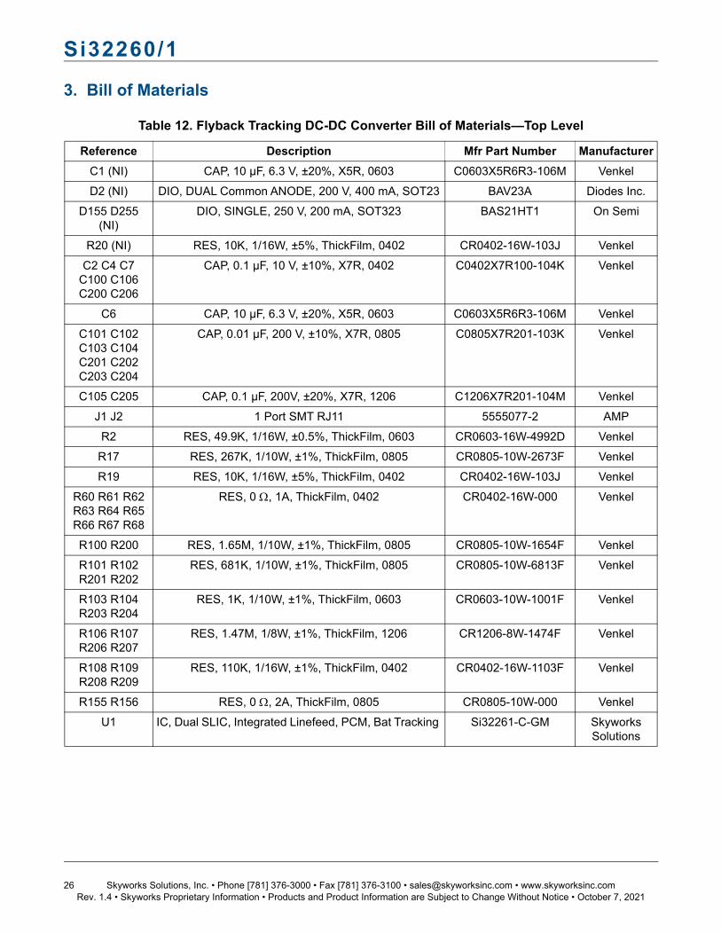
3. Bill of Materials
Table 12. Flyback Tracking DC-DC Converter Bill of Materials—Top Level
Reference Description Mfr Part Number Manufacturer
C1 (NI) CAP, 10 µF, 6.3 V, ±20%, X5R, 0603 C0603X5R6R3-106M Venkel
D2 (NI) DIO, DUAL Common ANODE, 200 V, 400 mA, SOT23 BAV23A Diodes Inc.
D155 D255 (NI)
DIO, SINGLE, 250 V, 200 mA, SOT323 BAS21HT1 On Semi
R20 (NI) RES, 10K, 1/16W, ±5%, ThickFilm, 0402 CR0402-16W-103J Venkel
C2 C4 C7 C100 C106 C200 C206
CAP, 0.1 µF, 10 V, ±10%, X7R, 0402 C0402X7R100-104K Venkel
C6 CAP, 10 µF, 6.3 V, ±20%, X5R, 0603 C0603X5R6R3-106M Venkel
C101 C102 C103 C104 C201 C202 C203 C204
CAP, 0.01 µF, 200 V, ±10%, X7R, 0805 C0805X7R201-103K Venkel
C105 C205 CAP, 0.1 µF, 200V, ±20%, X7R, 1206 C1206X7R201-104M Venkel
J1 J2 1 Port SMT RJ11 5555077-2 AMP
R2 RES, 49.9K, 1/16W, ±0.5%, ThickFilm, 0603 CR0603-16W-4992D Venkel
R17 RES, 267K, 1/10W, ±1%, ThickFilm, 0805 CR0805-10W-2673F Venkel
R19 RES, 10K, 1/16W, ±5%, ThickFilm, 0402 CR0402-16W-103J Venkel
R60 R61 R62 R63 R64 R65 R66 R67 R68
RES, 0 , 1A, ThickFilm, 0402 CR0402-16W-000 Venkel
R100 R200 RES, 1.65M, 1/10W, ±1%, ThickFilm, 0805 CR0805-10W-1654F Venkel
R101 R102 R201 R202
RES, 681K, 1/10W, ±1%, ThickFilm, 0805 CR0805-10W-6813F Venkel
R103 R104 R203 R204
RES, 1K, 1/10W, ±1%, ThickFilm, 0603 CR0603-10W-1001F Venkel
R106 R107 R206 R207
RES, 1.47M, 1/8W, ±1%, ThickFilm, 1206 CR1206-8W-1474F Venkel
R108 R109 R208 R209
RES, 110K, 1/16W, ±1%, ThickFilm, 0402 CR0402-16W-1103F Venkel
R155 R156 RES, 0 , 2A, ThickFilm, 0805 CR0805-10W-000 Venkel
U1 IC, Dual SLIC, Integrated Linefeed, PCM, Bat Tracking Si32261-C-GM Skyworks Solutions

Si32260/1
Skyworks Solutions, Inc. • Phone [781] 376-3000 • Fax [781] 376-3100 • [email protected] • www.skyworksinc.com 27Rev. 1.4 • Skyworks Proprietary Information • Products and Product Information are Subject to Change Without Notice • October 7, 2021
Table 13. Flyback Tracking DC-DC Converter Bill of Materials—DC-DC
Reference Description Mfr Part Number Manufacturer
C120 C220 (NI)
CAP, 10 µF, 25 V, ±20%, X7R, 1210 C1210X7R250-106M Venkel
C125 C225 (NI)
CAP, 0.1 µF, 200 V, ±20%, X7R, 1206 C1206X7R201-104M Venkel
C126 C226 (NI)
CAP, 470 pF, 100 V, ±10%, X7R, 0603 C0603X7R101-471K Venkel
D121 D221 (NI)
DIO, ZENER, 75 V, 200 mW, SOD323 BZX384C75-V Vishay
D122 D222 (NI)
DIO, SWITCH, 200mA, 75 V, SOD523 BAS16XV2T1G On Semi
R127 R227 (NI)
RES, 15 , 1/2W, ±5%, ThickFilm, 1210 CR1210-2W-150J Venkel
C121 C221 CAP, 0.1 µF, 50 V, ±10%, X7R, 0603 C0603X7R500-104K Venkel
C122 C123 C124 C222 C223 C224
CAP, 0.1 µF, 200 V, ±20%, X7R, 1206 C1206X7R201-104M Venkel
C130 CAP, 120 µF, 63 V, ±20%, AL, 8X16MM, Low Imped-ance
EEUFC1J121 Panasonic
D120 D220 DIO, FAST, 300V, 1A, SMA ES1F Fairchild
Q120 Q220 TRANSISTOR, MOSFET, N-CHNL, 2.0W Switching, Logic Level, SOT223
FQT7N10L Fairchild
R121 R221 RES, 0.1 , 1/2W, ±1%, ThickFilm, 1210 LCR1210-R100F Venkel
R122 R222 RES, 15 , 1/2W, ±5%, ThickFilm, 1210 CR1210-2W-150J Venkel
R123 R223 RES, 15 , 1/16W, ±1%, ThickFilm, 0402 CR0402-16W-15R0F Venkel
R124 R125 R224 R225
RES, 0 , 1A, ThickFilm, 0402 CR0402-16W-000 Venkel
R126 R226 RES, 68K, 1/16W, ±5%, ThickFilm, 0402 CR0402-16W-683J Venkel
T120 T220 TRANSFORMER, Flyback, 8.0uH Primary, 100nH Leakage, 1:3, 1 Tap, SMT
UTB01890s UMEC
Table 14. Flyback Tracking DC-DC Converter Bill of Materials—Protection
C108 C208 CAP, 0.01 µF, 200 V, ±10%, X7R, 0805 C0805X7R201-103K Venkel
C150 C250 CAP, 0.1 µF, 200 V, ±20%, X7R, 1206 C1206X7R201-104M Venkel
RF150 RF151 RF250 RF251
FUSE, 0.5A, 600 V B0500T Bourns
R150 R250 RES, 10 , 1/10W, ±1%, ThickFilm, 0805 CR0805-10W-10R0F Venkel
R151 R251 RES, 10 , 1/10W, ±1%, ThickFilm, 0805 CR0805-10W-10R0F Venkel
U151 U251 SLIC Protector TISP61089BDR Bourns

Si32260/1
28 Skyworks Solutions, Inc. • Phone [781] 376-3000 • Fax [781] 376-3100 • [email protected] • www.skyworksinc.comRev. 1.4 • Skyworks Proprietary Information • Products and Product Information are Subject to Change Without Notice • October 7, 2021
Table 15. Low Cost Quasi Ćuk (LCQC) DC-DC Converter Bill of Materials—Top Level
Reference Description Mfr Part Number Manufacturer
C2 (NI) 10UF, 6.3V, 20%, X5R, 0603 C0603X5R6R3-106M Venkel
C3 10UF, 6.3V, 20%, X5R, 0603 C0603X5R6R3-106M Venkel
C4 C5 C6 C100 C106 C200 C206
0.1UF, 10V,10%, X7R, 0402 C0402X7R100-104K Venkel
C105 C205 0.1UF, 250V, 10%, X7T, 0805 C2012X7T2E104K Tdk Corporation
C101 C102 C103 C104 C201 C202 C203 C204
.01UF, 200V, 10%, X7R, 0805 C0805X7R201-103K Venkel
R107 R108 R207 R208
110K 1% CR0402-16W-1103F Venkel
R14 49.9K, 1/16W, 0.5%, 0603 CR0603-16W-4992D Venkel
R9 R10 10K, 1/16W, 5%, 0402 CR0402-16W-103J Venkel
R100 R200 1.65M, 1/10W, 1%, 0805 CR0805-10W-1654F Venkel
R105 R106 R205 R206
1.47M, 1/8W, 1%, 1206 CR1206-8W-1474F Venkel
R103 R104 R203 R204
1K, 1/16W, 1%, 0402 CR0402-16W-1001F Venkel
R101 R102 R201 R202
681K, 1/10W, 1%, 0805 CR0805-10W-6813F Venkel
R17 267K, 1/16W, 1%, 0402 CR0402-16W-2673F Venkel
D3 D4 BAS21HT1 BAS21HT1 On Semi
J1 J2 RJ-11 5555077-2 Tyco
U61 SI32260 SI32260-C-GM2 Skyworks Solutions

Si32260/1
Skyworks Solutions, Inc. • Phone [781] 376-3000 • Fax [781] 376-3100 • [email protected] • www.skyworksinc.com 29Rev. 1.4 • Skyworks Proprietary Information • Products and Product Information are Subject to Change Without Notice • October 7, 2021
Table 16. Low Cost Quasi Ćuk (LCQC) DC-DC Converter Bill of Materials—DC-DC
Reference Description Mfr Part Number Manufacturer
C120 C220 2.2uf, 16V,20%, X7R, 0805 C0805X7R160-225M Venkel
C121 C221 0.1uf, 25V,20%, X7R, 0603 C0603X7R250-104M Venkel
C122 C123 C124 C125 C222 C223 C224 C225
0.1uf, 250V, 10%, X7T, 0805 C2012X7T2E104K TDK Corporation
D121 D221 BAV23C BAV23C Diodes Inc.
D123 D223 ES1D ES1D Diodes Inc.
L120 L220 15uH, 1.6A, 20%, shielded NR 6028T 150M Taiyo Yuden
Q120 Q220 FDT86244, 2.8A, 150V N-CHAN FDT86244 Fairchild
R128 R228 68k, 1/16W, 5%, 0402 CR0402-16W-683J Venkel
R129 R130 R229 R230
0 ohm, 1A, 0402 CR0402-16W-000 Venkel
R131 R132 R133 R134 R135 R231 R232 R233 R234 R235
1.0 ohm, 1/16W, 1%, 0402 CR0402-16W-1R00F Venkel
R122 R222 15 ohm, 1/10W, 1%, 0805 CR0805-10W-15R0F Venkel
Table 17. Low Cost Quasi Ćuk (LCQC) DC-DC Converter Bill of Materials—Protection
Reference Description Mfr Part Number Manufacturer
C108 C208 .01uf, 200V, 10%, X7R, 0805 C0805X7R201-103K Venkel
C150 C250 0.1uf, 250V, 10%, X7T, 0805 C2012X7T2E104K TDK Corporation
R150 R151 R250 R251
10 ohm, 1%, 0805 CR0805-10W-10R0F Venkel
RT150 RT151 RT250 RT251
PTC, 3A, 250V MF-SM013/250V Bourns
U151 U251 TISP61089BDR TISP61089BDR Bourns

Si32260/1
Skyworks Solutions, Inc. • Phone [781] 376-3000 • Fax [781] 376-3100 • [email protected] • www.skyworksinc.com 30Rev. 1.4 • Skyworks Proprietary Information • Products and Product Information are Subject to Change Without Notice • October 7, 2021
4. Functional Description
Figure 20. Functional Block Diagram
The Si32260/1 dual ProSLIC devices provide all SLIC,codec, DTMF detection, and signal generation functionsneeded for two complete analog telephone interfaces.They perform all battery, over-voltage, ringing,supervision, codec, hybrid, and test (BORSCHT)functions, and also support extensive metallic looptesting capabilities.
The Si32260/1 both provide a standard voice-band (200 Hz–3.4 kHz) audio codec and, optionally, an audiocodec with both wideband (50 Hz–7 kHz) and standardvoiceband modes. The wideband mode provides anexpanded audio band with a 16 kHz sample rate forenhanced audio quality while the standard voice-bandmode provides standard telephony audio bandwidth.
The Si32260/1 devices incorporate two programmabledc-dc converter controllers that can operate in eitherbattery tracking mode or a shared rail mode. In both thebattery tracking and the shared rail modes the dc-dcconverter controllers react to line conditions to providethe optimal battery voltage required for each line-state.Multiple Si32260/1 devices can also operate from fixedrail supplies controlled either by one of the integrateddc-dc controllers or by an external dc-dc controller. TheSi32260/1 devices are available with voltage ratings of –110 or –140 V to support a wide range of ringingvoltages. See Section "8. Ordering Guide‚" on page 45for the voltage rating of each version.
Programmable on-hook voltage, programmable offhookloop current, reverse battery operation, loop or groundstart operation, and on-hook transmission aresupported. Loop current and voltage are continuouslymonitored by an integrated monitoring ADC. TheSi32260/1 dual ProSLIC devices support balanced andunbalanced 5 REN ringing with or without aprogrammable dc offset, and can operate in low powerringing and adaptive ringing modes. The availableoffset, frequency, waveshape, and cadence options aredesigned to ring the widest variety of terminal devicesand to reduce external controller requirements.
A complete audio transmit and receive path isintegrated, including ac impedance and hybrid gain.These features are software-programmable, allowing asingle hardware design to meet global requirements.
SPIControl
Interface
PCM/GCI
Interface
DSP
DTMF &Tone Gen
Pro
gram
mab
le
AC
Impe
danc
ean
d H
ybrid
Caller ID
RingingGenerator
ADC
DAC
CODEC SLICLinefeedControl
LinefeedMonitor
DC-DC Controller
Line Diagnostics
PLLPCLK
FSYNC
DRX
DTX
CS
SDI
SDO
SCLK
INT
RST
SPIControl
Interface
PCM/GCI
Interface
DSP
DTMF &Tone Gen
Pro
gram
mab
le
AC
Impe
danc
ean
d H
ybrid
Caller ID
RingingGenerator
ADC
DAC
CODEC
DC-DC Controllers
Line Diagnostics
PLLPCLK
FSYNC
DRX
DTX
CS
SDI
SDO
SCLK
INT
RST
Si32260/1
DACRING
TIP
Line
feed
Channel A
CODEC SLIC
DACRING
TIP
Line
feed
Channel B
CODEC SLIC
ADC
ADC
LinefeedControl
LinefeedMonitor
LinefeedControl
LinefeedMonitor

Si32260/1
Skyworks Solutions, Inc. • Phone [781] 376-3000 • Fax [781] 376-3100 • [email protected] • www.skyworksinc.com 31Rev. 1.4 • Skyworks Proprietary Information • Products and Product Information are Subject to Change Without Notice • October 7, 2021
5. FXS Features
5.1. DC Feed CharacteristicsProSLIC internal linefeed circuitry provides completelyprogrammable dc feed characteristics.
When in the active state, the ProSLIC operates in one ofthree dc linefeed operating regions: a constant-voltageregion, a constant-current region, or a resistive region,as shown in Figure 21. The constant-voltage region hasa low resistance, typically 160 . The constant-currentregion approximates infinite resistance.
Figure 21. Dual ProSLIC DC Feed Characteristics
5.2. Linefeed Operating StatesThe linefeed interface includes nine different register-programmable operating states as listed in Table 18.The Open state is the default condition in the absenceof any preloaded register settings. The device may alsoautomatically enter the open state in the event of alinefeed fault condition.
5.3. Line Voltage and Current MonitoringThe ProSLIC continuously monitors the TIP, RING, andbattery voltages and currents via an on-chip ADC andstores the resulting values in individual RAM locations.Additionally, the loop voltage (VTIP–VRING), loop current,and longitudinal current values are calculated based onthe TIP and RING measurements and are stored inunique register locations for further processing. TheADC updates all registers at a rate of 2 kHz or greater.
5.4. Power Monitoring and Power Fault Detection
The Si32260/1 line monitoring functions are used tocontinuously protect against excessive powerconditions. The Si32260/1 contains on-chip, analogsensing diodes that turn off the device when a presettemperature threshold is exceeded.
If the Si32260/1 detects a fault condition or overpowercondition, it automatically sets that line to the open stateand generates a "power alarm" interrupt.
The interrupt can be masked, but masking theautomatic transition to open is not recommended.
The various power alarms and linefeed faults supportingautomatic intervention are described below.
1. Total power exceeded.
2. Excessive foreign current or voltage on TIP and/or RING.
3. Thermal shutdown event.
5.5. Thermal Overload ShutdownIf the die temperature exceeds the maximum junctiontemperature threshold (TJmax) of 145 or 200 °C,depending on the operating state, the device has theability to shut itself down to a low-power state withoutuser intervention.
ILOOP (mA)I_RFEED
VTR(V)
I_ILIMI_VLIM
Resistive Region
Con
stan
t I R
egio
n
Constant V RegionV_VLIM
V_RFEED
V_ILIM

Si32260/1
32 Skyworks Solutions, Inc. • Phone [781] 376-3000 • Fax [781] 376-3100 • [email protected] • www.skyworksinc.comRev. 1.4 • Skyworks Proprietary Information • Products and Product Information are Subject to Change Without Notice • October 7, 2021
Table 18. Linefeed Operating States
Linefeed State Description
Open Output is high-impedance and all line supervision functions are powered down. Audio is not transmitted. This is the default state after powerup or following a hardware reset. This state can also be used in the presence of line fault conditions and to generate open switch intervals (OSIs). This state is used in line diagnostics mode as a high impedance state during linefeed testing. A power fault condition may also force the device into the open state.
Forward ActiveReverse Active
Linefeed circuitry and audio are active. In Forward Active state, the TIP lead is more posi-tive than the RING lead; in Reverse Active state, the RING lead is more positive than the TIP lead. Loop closure and ground key detect circuitry are active.
Forward OHTReverse OHT
Provides data transmission during an on-hook loop condition (e.g., transmitting caller ID data between ringing bursts). Linefeed circuitry and audio are active. In Forward OHT state, the TIP lead is more positive than the RING lead; in Reverse OHT state, the RING lead is more positive than the TIP lead.
TIP Open Provides an active linefeed on the RING lead and sets the TIP lead to high impedance (>400 k) for ground start operation in forward polarity. Loop closure and ground key detect circuitry are active.
RING Open Provides an active linefeed on the TIP lead and sets the RING lead to high impedance (>400 k) for ground start operation in reverse polarity. Loop closure and ground key detect circuitry are active.
Ringing Drives programmable ringing signal onto TIP and RING leads with or without dc offset.
Line Diagnostics The channel is put into diagnostic mode. In this mode, the channel has special diagnostic resources available.

Si32260/1
Skyworks Solutions, Inc. • Phone [781] 376-3000 • Fax [781] 376-3100 • [email protected] • www.skyworksinc.com 33Rev. 1.4 • Skyworks Proprietary Information • Products and Product Information are Subject to Change Without Notice • October 7, 2021
5.6. Loop Closure DetectionThe Si32260/1 provides a completely programmableloop closure detection mechanism. The loop closuredetection scheme provides two unique thresholds toallow hysteresis, and also includes a programmabledebounce filter to eliminate false detection. A loopclosure detect status bit provides continuous status, anda maskable interrupt bit is also provided.
5.7. Ground Key DetectionThe Si32260/1 provides a ground key detectmechanism using a programmable architecture similarto the loop closure scheme. The ground key detectscheme provides two unique thresholds to allowhysteresis and also includes a programmable debouncefilter to eliminate false detection. A ground key detectstatus bit provides continuous status, and a maskableinterrupt bit is also provided.
5.8. Ringing GenerationThe Si32260/1 provides the ability to generate aprogrammable sinusoidal or trapezoidal ringingwaveform, with or without dc offset. The ringingfrequency, wave shape, cadence, and offset are allregister-programmable. Three ringing modes aresupported: balanced, unbalanced, and low-powerringing (LPR). Figure 22 illustrates the fundamentaldifferences between the three ringing modes.
The dual ProSLIC’s adaptive ringing capability allowsfurther power savings to be realized in systemsdesigned for long loop applications. In a long loopsystem, it may be necessary to generate a large ringingvoltage to ensure that sufficient voltage is presented toa phone at the far end of the loop. However, insituations when a short loop is connected to an FXSinterface that was designed with the ability to ring longloops, the large ringing voltage in combination with alow resistance load will result in excessive andunnecessary power consumption. Skyworks Solutions’Si32260/1 dual ProSLICs eliminate this unnecessarypower consumption with their adaptive ringingcapability. The ProSLIC automatically senses whenexcessive power is being consumed in the line feedcircuit (due to the lower resistance of a short loop) andwill iteratively reduce the ringing amplitude to a voltagethat is appropriate for the load.

Si32260/1
34 Skyworks Solutions, Inc. • Phone [781] 376-3000 • Fax [781] 376-3100 • [email protected] • www.skyworksinc.comRev. 1.4 • Skyworks Proprietary Information • Products and Product Information are Subject to Change Without Notice • October 7, 2021
Figure 22. Ringing Modes
Figure 23. Adaptive Ringing
TIPRINGVBAT
Balanced
VBAT
TIPRING
LPR
TIP
RINGVBAT
UnbalancedGND GND GND

Si32260/1
Skyworks Solutions, Inc. • Phone [781] 376-3000 • Fax [781] 376-3100 • [email protected] • www.skyworksinc.com 35Rev. 1.4 • Skyworks Proprietary Information • Products and Product Information are Subject to Change Without Notice • October 7, 2021
5.9. Polarity ReversalThe Si32260/1 supports polarity reversal for messagewaiting and various other signaling modes. The ramprate can be programmed for a smooth or abrupttransition to accommodate different applicationrequirements.
5.10. Two-Wire Impedance SynthesisThe ac two-wire impedance synthesis is generated on-chip using a DSP-based scheme to optimally match theoutput impedance of the Si32260/1 to the referenceimpedance. Most real or complex two-wire impedancescan be generated by using the coefficient generatorsoftware to simulate the desired line conditions andgenerate the required register coefficients.
5.11. Transhybrid Balance FilterThe trans-hybrid balance function is implemented on-chip using a DSP-based scheme to effectively cancelthe reflected receive path signal from the transmit path.The coefficient generator software is used to optimizethe filter coefficients.
5.12. Tone GeneratorsThe Si32260/1 includes two digital tone generators thatallow a wide variety of single- or dual-tone frequencyand amplitude combinations. Each tone generator hasits own set of registers that hold the desired frequency,amplitude, and cadence to allow generation of DTMFand call progress tones for different requirements. Thetones can be directed to either receive or transmit paths.
5.13. DTMF DetectionThe Dual ProSLIC performs DTMF detection.
5.14. Pulse MeteringThe pulse metering system for the Si32260/1Si32260/1is designed to inject a 12 or 16 kHz billing tone into theaudio path with maximum amplitude of 0.5 VRMS at TIPand RING into a 200 ac load impedance. The tone isgenerated in the DSP via a table lookup that guaranteesspectral purity by not allowing drift. The tone will rampup until it reaches a host-programmed threshold, atwhich point it will maintain that level until instructed toramp down, thus creating a trapezoidal envelope.
See AN381 for additional details and considerations onPulse Metering.
5.15. DC-DC ControllerThe Si3226x integrates two dc-dc controllers that canbe used to control external dc-dc converters to generatehigh voltage supplies to the SLIC channels.
The integrated line feeds are designed to work witheither a single tracking high voltage input, one for eachchannel, or with two high voltage supplies shared byboth channels.
In tracking mode, the VBATa and VBATb inputs areeach directly connected to the high voltage output oftwo tracking dc-dc converters, one for channel A andone for channel B. In tracking mode, the VBAT voltagefor each channel is optimized to minimize powerconsumption by closely tracking the SLIC state, eventracking the ringing waveforms (see section 2.1 forschematics).
In shared supply mode, a single flyback dc-dc convertergenerates two rails using two taps on the dc-dcconverter's transformer. External power offloadingtransistors are used to lower the power dissipated insidethe Si3226x device by shunting excess power away. Intracking shared supply (TSS) mode, in a two channelimplementation, the dc-dc converter is controlled by theintegrated dc-dc controller which allows the high voltageand low voltage outputs from the dc-dc converter totrack the combined state of the two channels of theSi3226x ProSLIC, including the ringing waveforms.Using the same schematic, the TSS mode of operationreduces system power consumption significantly whencompared to typical fixed rail shared supply designs(see section 2.2 for schematics).
Both of the dc-dc controller outputs DCDRVa/b aredriven by an internal charge pump which allows them toconnect directly to the gate of the MOSFET switch of aflyback (transformer based) dc-dc converter. Thisconnection eliminates the need for the MOSFET pre-drive circuit that is required when VTH is greater thanVDD. See Table 7.
5.16. Wideband AudioThe Si32260/1 dual ProSLIC devices support asoftware-selectable wideband (50 Hz–7 kHz) andnarrowband (200 Hz–3.4 kHz) audio codec. Thewideband mode provides an expanded audio band at a16-bit, 16 kHz sample rate for enhanced audio qualitywhile maintaining standard telephony audiocompatibility. In wideband operation, two time slots areused to transmit the wideband signal and each slotcontains 8-bits of the 16-bit sample. These two timeslots are transmitted and received half a frame apart,but within the same 8 kHz frame.

Si32260/1
36 Skyworks Solutions, Inc. • Phone [781] 376-3000 • Fax [781] 376-3100 • [email protected] • www.skyworksinc.comRev. 1.4 • Skyworks Proprietary Information • Products and Product Information are Subject to Change Without Notice • October 7, 2021
5.17. In-Circuit and Metallic Loop Testing (MLT)
A rich set of features is provided for in-circuit testing ofthe FXS system and the connected telephone line(MLT):
Tone generators
Audio diagnostic filters
Digital and analog loop-back modes
Internal test load
Monitor ADC
DSP algorithms
Using these facilities, it is possible to test theSi32260/1’s dc-dc converter, codec, line-feed, PCM businterface, DSP, SPI bus interface, and call progressstate-machine as well as testing the connectedtelephone line and external protection circuitry.
The audio diagnostic filters on the FXS are intended toprovide programmable filtering of the TX digital audiosignal and calculate the peak and/or average signalpower of the filters’ outputs. The signal powers are thencompared to programmable thresholds. Theprogrammable filters can be used to band-pass filter acertain tone or notch out certain tones, so that the signalpower measurements are frequency selective. Thisfiltering is useful in a telephony system because it canmeasure harmonic distortion, intermodulation, noise,etc.
The Si32260/1 incorporates an internal test load with a2.2 k nominal value that can be connected acrossTip/Ring (Figure 24). The audio diagnostics system andbuilt-in test load can be used to test the FXS interface(Si32260/1) itself without requiring an external load, aconnected line, or any relays. This facility can be usedfor production and in-service testing of such things as:
Dial tone draw/break
Audio quality measurements
Pulse digit detection
DC feed
Ringtrip
Polarity reversal
Transmission loss
MLT, e.g., GR-909, is facilitated by the built-in DSP,monitor ADC, and test load. They provide the ability todetect multiple fault conditions within the CPE as well ason the Tip/Ring pair (T-R). Thirteen different measuredand/or calculated parameters are reported by theMonitor ADC. Host software for use in conjunction withthe ProSLIC API is available from Skyworks Solutions.Typical MLT tests include:
Hazardous Potential Test – This checks for ac voltage > 50 VRMS or dc voltage > 135 V between Tip and Ground (T-G) or Ring and Ground (R-G).
Foreign Electromotive Force Test – Checks T-G or R-G for ac voltage > 10 VRMS or dc voltage > 6 V. Uses same threshold as for hazardous voltage test.
Resistive Faults Test – Checks for dc resistance from T-R, T-G or R-G. Any measurement < 150 k is considered a resistive fault.
Receiver-Off-Hook Test – Distinguishes between a T-R resistive fault and an off-hook condition.
Ringers Test – Measures the magnitude of the connected ring load (REN) across T-R. Results are > 0.175 REN and < 5 REN for a valid load
AC Line Impedance (line length) – T-R, T-G, and R-G. Generates a tone at several specific frequencies (audio band) and measures the reflected signal amplitude (complex spectrum) that comes back (with transhybrid balance filter disabled). The reflected signal is then used to calculate the line impedance based on certain assumptions of wire gauge, etc.
Line Capacitance – T-R, T-G, R-G. Generates a linear ramp function with polarity reversal, and measures the time constant.
Diagnostic information is available even in the presenceof fault conditions that cause the system’s protectiondevices (fuses, PTCs, etc.) to open. A high-impedancesensing path (pins SRINGC and STIPC) can be used tomeasure the conditions on Tip/Ring even when the FXSsystem is effectively disconnected from the line. Norelay is required and this sensing path inherently meetsDielectric Withstand per GR-49 (> 1000 V).
Figure 24. Si32260/1 Internal Test Load Circuit
TIP
RING
Test Load
RTL = 2.2 k (typical)

Si32260/1
Skyworks Solutions, Inc. • Phone [781] 376-3000 • Fax [781] 376-3100 • [email protected] • www.skyworksinc.com 37Rev. 1.4 • Skyworks Proprietary Information • Products and Product Information are Subject to Change Without Notice • October 7, 2021
6. System Interfaces
6.1. SPI Control InterfaceThe controller interface to the Si32260/1 is a 4-wireinterface modeled after microcontroller and serialperipheral devices. The interface consists of a clock(SCLK), chip select (CS), serial data input (SDI), andserial data output (SDO). In addition, the ProSLICdevices feature a serial data through output (SDITHRU8x8 mm package only) to support operation of up to 16channels using a single chip select line. Each FXS portoccupies one SPI channel. The device operates withboth 8-bit and 16-bit SPI controllers.
6.2. PCM Interface and CompandingThe Si32260/1 contains a flexible, programmableinterface for the transmission and reception of digitalPCM samples. PCM data transfer is controlled by thePCM clock (PCLK) and frame sync (FSYNC) inputs aswell as the PCM Mode Select, PCM Transmit Start, andPCM Receive Start settings.
The interface can be configured to support from 8 to128 8-bit time slots in each 125 µs frame,corresponding to a PCM clock (PCLK) frequency rangeof 512 kHz to 8.192 MHz. 1.544 MHz is also supported.
The Si32260/1 supports both µ-255 Law (µ-Law) and A-law companding formats in addition to 16-bit linear datamode with no companding.

Si32260/1
38 Skyworks Solutions, Inc. • Phone [781] 376-3000 • Fax [781] 376-3100 • [email protected] • www.skyworksinc.comRev. 1.4 • Skyworks Proprietary Information • Products and Product Information are Subject to Change Without Notice • October 7, 2021
7. Pin Descriptions: Si32260/1
7.1. Si32260/61 6x8 mm Package
Pin # Pin Name Description
1 GPIO2a/SRINGCaGeneral Purpose I/O or RING Coarse Sense Input—Channel A.RING channel A Voltage sensing outside protection circuit.
2 GPIO1a/STIPCaGeneral Purpose I/O or TIP Coarse Sense Input—Channel A.TIP channel A voltage sensing outside protection circuit.
3 SRINGDCaRING DC Sense Input—Channel A.Analog dc input to sense voltage on the channel A RING lead.
4 SRINGACaRING AC Sense Input—Channel A.Analog ac input to sense voltage on the channel A RING lead.
5 STIPACaTIP AC Sense Input—Channel A.Analog ac input to sense voltage on the channel A TIP lead.
6 STIPDCaTIP DC Sense Input—Channel A.Analog dc input to sense voltage on the channel A TIP lead.
7 CAPPaSLIC Stabilization Capacitor—Channel A.Capacitor used in low pass filter.
8 CAPMaSLIC Stabilization Capacitor—Channel A.Capacitor used in low pass filter.
9 SVBATaVBAT Sense—Channel A.Input to sense voltage on VBAT.
10 SVDCDC-DC Input Voltage Sensor.Senses VDC input to dc-dc converters.
1
2
3
4
5
6
7
8
9
10
11
12
13
14
15
16
HVPAD
GNDPAD
TIP
a
TIP
b
RIN
Gb
VB
AT
b
VB
AT
a
RIN
Ga
GPIO1a / STIPCa
SRINGDCa
SRINGACa
STIPACa
STIPDCa
CAPPa
CAPMa
SVBATa
SVDC
RSTB
INTB / DTXENB
FSYNC
PCLK
DTX
GPIO2A / SRINGCa
DRX
SD
CH
a
SD
CL
a
DC
DR
Va
DC
FF
a
DC
FF
b
DC
DR
Vb
SD
CL
b
SD
CH
b
VD
DD
28
31
26
27
29
30
32
33
34
35
36
37
38
39
40
41
2524232221201917 18
4647
45 44
43
42
VDDREG
CSB
SCLK
SDO
SDI
SVBATb
CAPMb
CAPPb
IREF
STIPDCb
STIPACb
SRINGACb
SRINGDCb
GPIO1b / STIPCb
GPIO2b / SRINGCb
VDDA

Si32260/1
Skyworks Solutions, Inc. • Phone [781] 376-3000 • Fax [781] 376-3100 • [email protected] • www.skyworksinc.com 39Rev. 1.4 • Skyworks Proprietary Information • Products and Product Information are Subject to Change Without Notice • October 7, 2021
11 RSTBReset Input.Active low input. Hardware reset used to place all control registers in the default state.
12 INTB/DTXENBInterrupt Output or Transmit PCM Data Output Enable.Maskable interrupt output or output enable for PCM data output. Open drain output for wire-ORed operation.
13 FSYNCFrame Sync Clock Input.8 kHz frame synchronization signal for the PCM bus. May be short or long pulse format.
14 PCLKPCM Bus Clock Input.Clock input for PCM bus timing.
15 DTXTransmit PCM Data Output.Output data to PCM bus.
16 DRXTransmit PCM Data Input.Input data from PCM bus.
17 SDCHaDC Monitor—Channel A.DC-DC converter monitor input used to detect overcurrent situations.
18 SDCLaDC Monitor—Channel A.DC-DC converter monitor input used to detect overcurrent situations.
19 DCDRVaDC Drive—Channel A.DC-DC converter control signal output which drives external transistor.
20 DCFFaDC Flexible Function—Channel A.DC-DC controller flexible function I/O—channel A.
21 DCFFbDC Flexible Function—Channel B.DC-DC controller flexible function I/O—channel B.
22 DCDRVbDC Drive—Channel B.DC-DC converter control signal output which drives external transistor.
23 SDCLbDC Monitor—Channel B.DC-DC converter monitor input used to detect overcurrent situations.
24 SDCHbDC Monitor—Channel B.DC-DC converter monitor input used to detect overcurrent situations.
25 VDDDIC Voltage Supply.Digital power supply for internal digital circuitry.
26 VDDREG Regulated Core Power Supply.
27 CSBChip Select Input.Active low. When inactive, SCLK and SDI are ignored and SDO is high impedance. When active, the serial port is operational.
28 SCLKSerial Port Bit Clock Input.Serial port clock input. Controls the serial data on SDO and latches the data on SDI.
29 SDOSerial Port Data Output.Serial port control data output.
Pin # Pin Name Description

Si32260/1
40 Skyworks Solutions, Inc. • Phone [781] 376-3000 • Fax [781] 376-3100 • [email protected] • www.skyworksinc.comRev. 1.4 • Skyworks Proprietary Information • Products and Product Information are Subject to Change Without Notice • October 7, 2021
30 SDISerial Port Data Input.Serial port control data input.
31 SVBATbVBAT Sense—Channel B.Input to sense voltage on VBAT.
32 CAPMbSLIC Stabilization Capacitor—Channel B.Capacitor used in low pass filter.
33 CAPPbSLIC Stabilization Capacitor—Channel B.Capacitor used in low pass filter.
34 IREFCurrent Reference Input.Connects to an external resistor used to provide a high accuracy reference current.
35 STIPDCbTIP DC Sense Input—Channel B.Analog dc input to detect voltage on the channel B TIP lead.
36 STIPACbTIP AC Sense Input—Channel B.Analog ac input to sense voltage on the channel B TIP lead.
37 SRINGACbRING AC Sense Input—Channel B.Analog ac input to sense voltage on the channel B RING lead.
38 SRINGDCbRING DC Sense Input—Channel B.Analog dc input to sense voltage on the channel B RING lead.
39 GPIO1b/STIPCbGeneral Purpose I/O or TIP Coarse Sense Input—Channel B.TIP channel A voltage sensing outside protection circuit.
40 GPIO2b/SRINGCbGeneral Purpose I/O or RING Coarse Sense Input—Channel B.RING channel A Voltage sensing outside protection circuit.
41 VDDAAnalog Supply Voltage.Analog power supply for internal analog circuitry.
42 TIPbTIP Terminal—Channel B.Connect to the TIP lead of the channel B subscriber loop.
43 RINGbRING Terminal—Channel B.Connect to the RING lead of the channel B subscriber loop.
44 VBATbBattery Voltage Supply—Channel B.Connect to battery supply for Channel B.
45 VBATaBattery Voltage Supply—Channel A.Connect to battery supply for Channel A.
46 RINGaRING Terminal—Channel A.Connect to the RING lead of the channel A subscriber loop.
47 TIPaTIP Terminal—Channel A.Connect to the TIP lead of the channel A subscriber loop.
48 HVPADExposed paddle.Connect to electrically-isolated low thermal impedance inner layer and/or backside thermal plane using multiple thermal vias.
49 GNDPADExposed paddle.Connect to ground.
Pin # Pin Name Description

Si32260/1
Skyworks Solutions, Inc. • Phone [781] 376-3000 • Fax [781] 376-3100 • [email protected] • www.skyworksinc.com 41Rev. 1.4 • Skyworks Proprietary Information • Products and Product Information are Subject to Change Without Notice • October 7, 2021
7.2. Si32260/61 8x8 mm Package
Pin # Pin Name Description
1 TIPaTIP Terminal—Channel A.Connect to the TIP lead of the channel A subscriber loop.
2 N/CNo Connect.This pin should be left unconnected.
3 GPIO2a/SRINGCaGeneral Purpose I/O or RING Coarse Sense Input—Channel A.RING channel A Voltage sensing outside protection circuit.
4 GPIO1a/STIPCaGeneral Purpose I/O or TIP Coarse Sense Input—Channel A.TIP channel A voltage sensing outside protection circuit.
5 SRINGDCaRING DC Sense Input—Channel A.Analog dc input to sense voltage on the channel A RING lead.
6 SRINGACaRING AC Sense Input—Channel A.Analog ac input to sense voltage on the channel A RING lead.
7 STIPACaTIP AC Sense Input—Channel A.Analog ac input to sense voltage on the channel A TIP lead.
8 STIPDCaTIP DC Sense Input—Channel A.Analog dc input to sense voltage on the channel A TIP lead.
9 CAPPaSLIC Stabilization Capacitor—Channel A.Capacitor used in low pass filter.
1
2
3
4
5
6
7
8
9
10
11
12
13
14
15
16 17 18 19 20 21 22 23 24 25 26 27 28 29 30 31
32
33
34
35
36
37
38
39
40
41
42
43
44
45
464748495051525354555657585960TIPa
N/C
GPIO2A / SRINGCa
GPIO1a / STIPCa
SRINGDCa
SRINGACa
STIPACa
STIPDCa
CAPPa
CAPMa
SVBATa
SVDC
RSTB
INTB / DTXENB
FSYNC
SD
ITH
RU
PC
LK
DA
TA
o
DA
TA
i
SD
CH
a
SD
CL
a
DC
DR
Va
AU
Xoi
AU
Xd
rv
DC
DR
Vb
SD
CLb
SD
CH
b
VD
DD
VD
DR
EG
CS
B
SC
LK
SDO
SDI
SVBATb
CAPMb
CAPPb
IREF
STIPDCb
STIPACb
SRINGACb
SRINGDCb
GPIO1b / STIPCb
GPIO2b / SRINGCb
VDDA
N/C
TIPb
N/C
RIN
Gb
VB
AT
b
N/C
BA
SE
b
N/C
N/C
N/C
N/C
N/C
BA
T_P
O
BA
SE
a
VB
AT
a
RIN
Ga
HVPAD
GND PAD

Si32260/1
42 Skyworks Solutions, Inc. • Phone [781] 376-3000 • Fax [781] 376-3100 • [email protected] • www.skyworksinc.comRev. 1.4 • Skyworks Proprietary Information • Products and Product Information are Subject to Change Without Notice • October 7, 2021
10 CAPMaSLIC Stabilization Capacitor—Channel A.Capacitor used in low pass filter.
11 SVBATaVBAT Sense—Channel A.Input to sense voltage on VBAT.
12 SVDCDC-DC Input Voltage Sensor.Senses VDC input to dc-dc converters.
13 RSTReset Input.Active low input. Hardware reset used to place all control registers in the default state.
14 INTB/DTXENBInterrupt Output or Transmit PCM Data Output Enable.Maskable interrupt output or output enable for PCM data output. Open drain output for wire-ORed operation.
15 FSYNCFrame Sync Clock Input.8 kHz frame synchronization signal for the PCM bus. May be short or long pulse format.
16 SDITHRUSDI Pass-Through.Cascaded SDI output signal for daisy-chain mode.
17 PCLKPCM Bus Clock Input.Clock input for PCM bus timing.
18 DTXTransmit PCM Data Output.Output data to PCM bus.
19 DRXTransmit PCM Data Input.Input data from PCM bus.
20 SDCHaDC Monitor—Channel A.DC-DC converter monitor input used to detect overcurrent situations.
21 SDCLaDC Monitor—Channel A.DC-DC converter monitor input used to detect overcurrent situations.
22 DCDRVaDC Drive—Channel A.DC-DC converter control signal output which drives external transistor.
23 DCFFaDC Flexible Function—Channel A.DC-DC controller flexible function I/O—channel A.
24 DCFFbDC Flexible Function—Channel B.DC-DC controller flexible function I/O—channel B.
25 DCDRVbDC Drive—Channel B.DC-DC converter control signal output which drives external transistor.
26 SDCLbDC Monitor—Channel B.DC-DC converter monitor input used to detect overcurrent situations.
27 SDCHbDC Monitor—Channel B.DC-DC converter monitor input used to detect overcurrent situations.
28 VDDDIC Voltage Supply.Digital power supply for internal digital circuitry.
29 VDDREG Regulated Core Power Supply.
Pin # Pin Name Description

Si32260/1
Skyworks Solutions, Inc. • Phone [781] 376-3000 • Fax [781] 376-3100 • [email protected] • www.skyworksinc.com 43Rev. 1.4 • Skyworks Proprietary Information • Products and Product Information are Subject to Change Without Notice • October 7, 2021
30 CSBChip Select Input.Active low. When inactive, SCLK and SDI are ignored and SDO is high impedance. When active, the serial port is operational.
31 SCLKSerial Port Bit Clock Input.Serial port clock input. Controls the serial data on SDO and latches the data on SDI.
32 SDOSerial Port Data Output.Serial port control data output.
33 SDISerial Port Data Input.Serial port control data input.
34 SVBATbVBAT Sense—Channel B.Input to sense voltage on VBAT.
35 CAPMbSLIC Stabilization Capacitor—Channel B.Capacitor used in low pass filter.
36 CAPPbSLIC Stabilization Capacitor—Channel B.Capacitor used in low pass filter.
37 IREFCurrent Reference Input.Connects to an external resistor used to provide a high accuracy reference current.
38 STIPDCbTIP DC Sense Input—Channel B.Analog dc input to detect voltage on the channel B TIP lead.
39 STIPACbTIP AC Sense Input—Channel B.Analog ac input to sense voltage on the channel B TIP lead.
40 SRINGACbRING AC Sense Input—Channel B.Analog ac input to sense voltage on the channel B RING lead.
41 SRINGDCbRING DC Sense Input—Channel B.Analog dc input to sense voltage on the channel B RING lead.
42 GPIO1b/STIPCbGeneral Purpose I/O or TIP Coarse Sense Input—Channel B.TIP channel A voltage sensing outside protection circuit.
43 GPIO2b/SRINGCbGeneral Purpose I/O or RING Coarse Sense Input—Channel B.RING channel A Voltage sensing outside protection circuit.
44 VDDAAnalog Supply Voltage.Analog power supply for internal analog circuitry.
45 N/CNo Connect.This pin should be left unconnected.
46 TIPbTIP Terminal—Channel B.Connect to the TIP lead of the channel B subscriber loop.
47 N/CNo Connect.This pin should be left unconnected.
48 RINGbRING Terminal—Channel B.Connect to the RING lead of the channel B subscriber loop.
49 N/CNo Connect.This pin should be left unconnected.
Pin # Pin Name Description
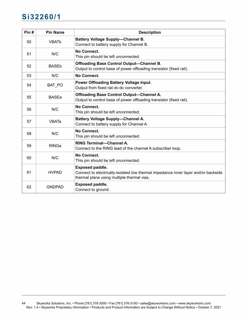
Si32260/1
44 Skyworks Solutions, Inc. • Phone [781] 376-3000 • Fax [781] 376-3100 • [email protected] • www.skyworksinc.comRev. 1.4 • Skyworks Proprietary Information • Products and Product Information are Subject to Change Without Notice • October 7, 2021
50 VBATbBattery Voltage Supply—Channel B.Connect to battery supply for Channel B.
51 N/CNo Connect.This pin should be left unconnected.
52 BASEbOffloading Base Control Output—Channel B.Output to control base of power offloading transistor (fixed rail).
53 N/C No Connect.
54 BAT_POPower Offloading Battery Voltage Input.Output from fixed rail dc-dc converter.
55 BASEaOffloading Base Control Output—Channel A.Output to control base of power offloading transistor (fixed rail).
56 N/CNo Connect.This pin should be left unconnected.
57 VBATaBattery Voltage Supply—Channel A.Connect to battery supply for Channel A.
58 N/CNo Connect.This pin should be left unconnected.
59 RINGaRING Terminal—Channel A.Connect to the RING lead of the channel A subscriber loop.
60 N/CNo Connect.This pin should be left unconnected.
61 HVPADExposed paddle.Connect to electrically-isolated low thermal impedance inner layer and/or backside thermal plane using multiple thermal vias.
62 GNDPADExposed paddle.Connect to ground.
Pin # Pin Name Description

Si32260/1
Skyworks Solutions, Inc. • Phone [781] 376-3000 • Fax [781] 376-3100 • [email protected] • www.skyworksinc.com 45Rev. 1.4 • Skyworks Proprietary Information • Products and Product Information are Subject to Change Without Notice • October 7, 2021
8. Ordering Guide
Table 19. Si32260/61 Ordering Guide1
P/N Description Package
Type
Package Size
Number of pins
Max VBAT
Temperature
Si32260-C-FM1 Dual wideband FXS, tracking or shared dc-dc
LGA2 8x8 mm 60 –110 V 0 to 70 °C
Si32260-C-GM1 Dual wideband FXS, tracking or shared dc-dc
LGA2 8x8 mm 60 –110 V –40 to 85 °C
Si32261-C-FM1 Dual wideband FXS, tracking or shared dc-dc
LGA2 8x8 mm 60 –140 V 0 to 70 °C
Si32261-C-GM1 Dual wideband FXS, tracking or shared dc-dc
LGA2 8x8 mm 60 –140 V –40 to 85 °C
Si32260-C-FM2 Dual wideband FXS, tracking dc-dc
LGA2 6x8 mm 47 –110 V 0 to 70 °C
Si32260-C-GM2 Dual wideband FXS, tracking dc-dc
LGA2 6x8 mm 47 –110 V –40 to 85 °C
Si32261-C-FM2 Dual wideband FXS, tracking dc-dc
LGA2 6x8 mm 47 –140 V 0 to 70 °C
Si32261-C-GM2 Dual wideband FXS, tracking dc-dc
LGA2 6x8 mm 47 –140 V –40 to 85 °C
Notes:1. Adding the suffix "R" to the part number (e.g., Si32260-C-FM1R) denotes tape and reel.2. LGA - Land Grid Array.

Si32260/1
46 Skyworks Solutions, Inc. • Phone [781] 376-3000 • Fax [781] 376-3100 • [email protected] • www.skyworksinc.comRev. 1.4 • Skyworks Proprietary Information • Products and Product Information are Subject to Change Without Notice • October 7, 2021
Table 20. Evaluation Kit Ordering Guide
Part Number Supported ProSLIC
Description VBAT Max
Interface
Si32260CQC20SL0EVB Si32260 Low cost quasi-Ćuk (NMOS FET/Inductor based) full tracking dc-dc
converter EVB
–110 V* PCM/SPI to VoiceMotherboard
Si32260CTS20SL0EVB Si32260 Tracking Shared Supply (TSS) dc-dcconverter EVB
–100 V PCM/SPI to VoiceMotherboard
Si32261CFB20SL0EVB Si32260, Si32261
Flyback (transformer based) fulltracking dc-dc converter EVB
–140 V PCM/SPI to VoiceMotherboard
Si32261CQC20SL0EVB Si32260, Si32261
Quasi-Ćuk (NMOS FET/Inductorbased) full tracking dc-dc converter
EVB
–140 V PCM/SPI to VoiceMotherboard
*Note: Supports VBAT up to –125 V with minor component substitutions (see AN381).

Si32260/1
Skyworks Solutions, Inc. • Phone [781] 376-3000 • Fax [781] 376-3100 • [email protected] • www.skyworksinc.com 47Rev. 1.4 • Skyworks Proprietary Information • Products and Product Information are Subject to Change Without Notice • October 7, 2021
9. Product Identification
The product identification number is a finished goods part number or is specified by a finished goods part number,such as a special customer part number.
Example:
Si32260-C-FM1R
Shipping Option Blank = TraysR = Tape and ReelProduct Revision
Product Designator
Package Type M2 = QFN/LGA-47M1 = QFN/LGA-60
Part Type / Lead Finish F = Commercial / RoHS-CompliantG = Industrial / RoHS-Compliant

Si32260/1
48 Skyworks Solutions, Inc. • Phone [781] 376-3000 • Fax [781] 376-3100 • [email protected] • www.skyworksinc.comRev. 1.4 • Skyworks Proprietary Information • Products and Product Information are Subject to Change Without Notice • October 7, 2021
10. Package Outlines
10.1. 47-Pin QFN/LGA (6x8 mm)
Figure 25. 47-pin QFN Package
Table 21. 47-Pin QFN Package Diagram Dimensions
Dimension MIN NOM MAX Dimension MIN NOM MAX
A 0.74 0.84 0.94 E5 3.30 3.35 3.40
b 0.20 0.25 0.30 f 0.80 BSC
D 6.00BSC L 0.35 0.40 0.45
D2 3.95 4.00 4.05 L1 0.05 0.10 0.15
e 0.50 BSC aaa — — 0.15
E 8.00 BSC bbb — — 0.15
E2 2.95 3.10 3.25 ccc — — 0.10
E3 2.00 2.15 2.30 ddd — — 0.10
E4 3.15 3.20 3.25
Notes:1. All dimensions shown are in millimeters (mm) unless otherwise noted.2. Dimensioning and Tolerancing per ANSI Y14.5M-1994.3. Recommended card reflow profile is per the JEDEC/IPC J-STD-020 specification for Small Body
Components.

Si32260/1
Skyworks Solutions, Inc. • Phone [781] 376-3000 • Fax [781] 376-3100 • [email protected] • www.skyworksinc.com 49Rev. 1.4 • Skyworks Proprietary Information • Products and Product Information are Subject to Change Without Notice • October 7, 2021
10.2. 60-Pin QFN/LGA (8x8 mm)
Figure 26. 60-Pin (QFN/LGA Package)
Table 22. 60-Pin QFN/LGA Package Diagram Dimensions
Dimension Min Nom Max Dimension Min Nom Max
A 0.74 0.84 0.94 E3 7.50 BSC.
b 0.20 0.25 0.30 E4 2.46 2.51 2.56
c 0.25 0.30 0.35 E5 3.34 3.39 3.44
D 8.00 BSC. L 0.35 0.40 0.45
D2 6.35 6.40 6.45 L1 0.05 0.10 0.15
D3 7.50 BSC. aaa — — 0.15
e 0.50 BSC. bbb — — 0.15
E 8.00 BSC. ccc — — 0.10
E2 6.35 6.40 6.45 ddd — — 0.10
Notes:1. All dimensions shown are in millimeters (mm) unless otherwise noted.2. Dimensioning and Tolerancing per ANSI Y14.5M-1994.3. Recommended card reflow profile is per the JEDEC/IPC J-STD-020 specification for Small Body
Components.
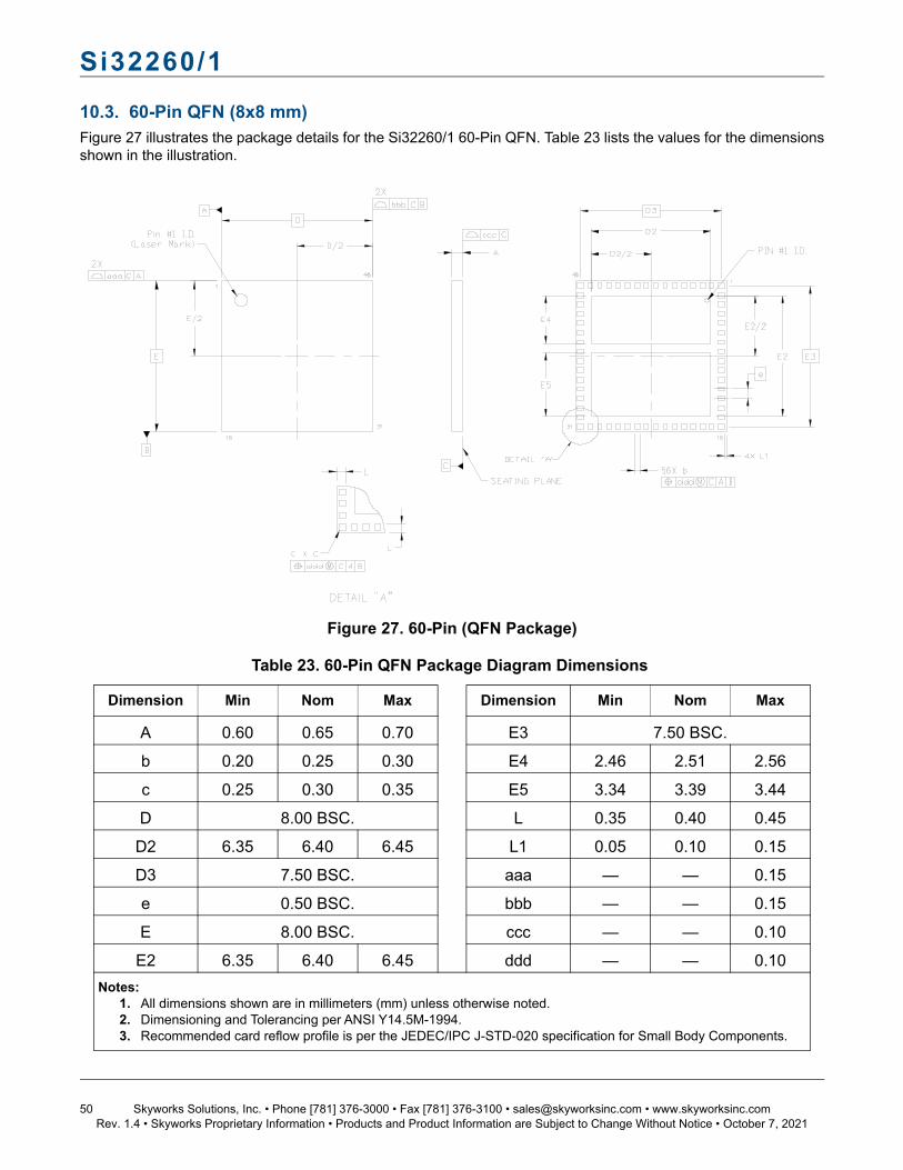
Si32260/1
50 Skyworks Solutions, Inc. • Phone [781] 376-3000 • Fax [781] 376-3100 • [email protected] • www.skyworksinc.comRev. 1.4 • Skyworks Proprietary Information • Products and Product Information are Subject to Change Without Notice • October 7, 2021
10.3. 60-Pin QFN (8x8 mm)Figure 27 illustrates the package details for the Si32260/1 60-Pin QFN. Table 23 lists the values for the dimensionsshown in the illustration.
Figure 27. 60-Pin (QFN Package)
Table 23. 60-Pin QFN Package Diagram Dimensions
Dimension Min Nom Max Dimension Min Nom Max
A 0.60 0.65 0.70 E3 7.50 BSC.
b 0.20 0.25 0.30 E4 2.46 2.51 2.56
c 0.25 0.30 0.35 E5 3.34 3.39 3.44
D 8.00 BSC. L 0.35 0.40 0.45
D2 6.35 6.40 6.45 L1 0.05 0.10 0.15
D3 7.50 BSC. aaa — — 0.15
e 0.50 BSC. bbb — — 0.15
E 8.00 BSC. ccc — — 0.10
E2 6.35 6.40 6.45 ddd — — 0.10
Notes:1. All dimensions shown are in millimeters (mm) unless otherwise noted.2. Dimensioning and Tolerancing per ANSI Y14.5M-1994.3. Recommended card reflow profile is per the JEDEC/IPC J-STD-020 specification for Small Body Components.
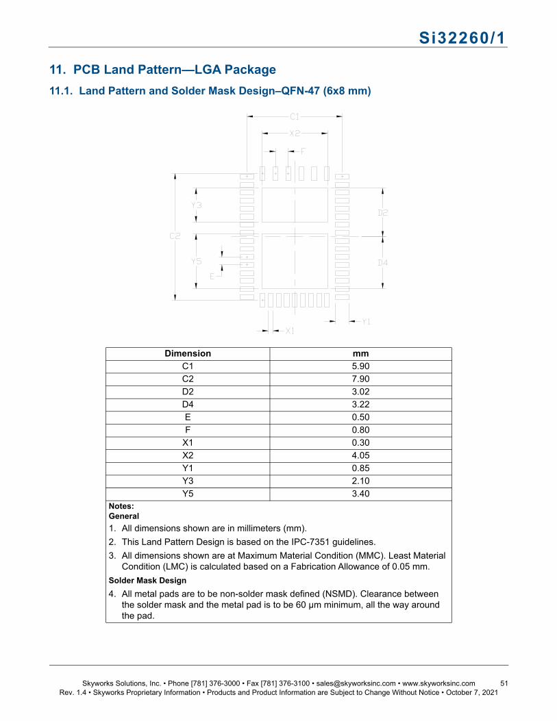
Si32260/1
Skyworks Solutions, Inc. • Phone [781] 376-3000 • Fax [781] 376-3100 • [email protected] • www.skyworksinc.com 51Rev. 1.4 • Skyworks Proprietary Information • Products and Product Information are Subject to Change Without Notice • October 7, 2021
11. PCB Land Pattern—LGA Package
11.1. Land Pattern and Solder Mask Design–QFN-47 (6x8 mm)
Dimension mm
C1 5.90
C2 7.90
D2 3.02
D4 3.22
E 0.50
F 0.80
X1 0.30
X2 4.05
Y1 0.85
Y3 2.10
Y5 3.40Notes:General
1. All dimensions shown are in millimeters (mm).
2. This Land Pattern Design is based on the IPC-7351 guidelines.
3. All dimensions shown are at Maximum Material Condition (MMC). Least Material Condition (LMC) is calculated based on a Fabrication Allowance of 0.05 mm.
Solder Mask Design
4. All metal pads are to be non-solder mask defined (NSMD). Clearance between the solder mask and the metal pad is to be 60 µm minimum, all the way around the pad.

Si32260/1
52 Skyworks Solutions, Inc. • Phone [781] 376-3000 • Fax [781] 376-3100 • [email protected] • www.skyworksinc.comRev. 1.4 • Skyworks Proprietary Information • Products and Product Information are Subject to Change Without Notice • October 7, 2021
11.2. Land Pattern and Solder Mask Design–QFN-60 (8x8 mm)
Dimension mm
C1 7.90
C2 7.90
D1 7.85
D2 7.85
E 0.50
f 0.65
X1 0.30
X2 6.35
Y1 0.85
Y2 2.46
Y3 3.39
Y4 6.37
Notes:General
1. All dimensions shown are in millimeters (mm).2. This Land Pattern Design is based on the IPC-7351 guidelines.3. All dimensions shown are at Maximum Material Condition (MMC). Least Material Condition
(LMC) is calculated based on a Fabrication Allowance of 0.05 mm.Solder Mask Design
4. All metal pads are to be non-solder mask defined (NSMD). Clearance between the solder mask and the metal pad is to be 60 µm minimum, all the way around the pad.

Si32260/1
Skyworks Solutions, Inc. • Phone [781] 376-3000 • Fax [781] 376-3100 • [email protected] • www.skyworksinc.com 53Rev. 1.4 • Skyworks Proprietary Information • Products and Product Information are Subject to Change Without Notice • October 7, 2021
11.3. Thermal via Layout–QFN-47 (6x8 mm)The thermal via layout rules in section “11.4. Thermal via Layout–QFN-60 (8x8 mm)” for the QFN-60 packageapply, except that it is not required to meet the minimum dimension d > 1.0 mm for the via edge to pin pad metalspacing, as described in note 4.
11.4. Thermal via Layout–QFN-60 (8x8 mm)
Dimension Min Max
d 1.00 —
Kx — 5.05
Ky — 5.05
Notes:1. High-Tg PCB materials (Tg ≥ 170 °C) are recommended for Pb-Free reflow profiles, per
standard industry practice. 2. The customer’s PCB design must provide sufficient thermal dissipation for high power
operation of the device. See layout guidelines in application note, “AN381: Si3226x ProSLIC Designer’s Guide”, for further details.
3. A minimum of eight thermal vias are required in each center pad. The recommended via diameter is 0.20–0.30 mm (8–12 mils).
4. Thermal vias placed in the center pads must have a minimum spacing of 1.0 mm from the edge of the via to the closest pin pad metal (d ≥ 1.0 mm).
5. Vias may be placed as desired within the non-hatched area of the center pads. 6. Vias placed within the center pad areas must be either filled, or tented on the top side of the
board, to prevent solder thieving from under the device.

Si32260/1
54 Skyworks Solutions, Inc. • Phone [781] 376-3000 • Fax [781] 376-3100 • [email protected] • www.skyworksinc.comRev. 1.4 • Skyworks Proprietary Information • Products and Product Information are Subject to Change Without Notice • October 7, 2021
11.5. Stencil Aperture Design–QFN-47 (6x8 mm)
Dimension mm
C1 5.90
C2 7.90
E 0.50
F 0.80
G 1.30
H 1.80
P1 1.80
P2 0.73
P3 2.33
P4 2.08
X1 0.30
Y1 0.85
Notes:Stencil Design
1. A stainless steel, laser-cut and electro-polished stencil with trapezoidal walls should be used to assure good solder paste release.
2. The stencil thickness should be 0.125 mm (5 mils).
Card Assembly
3. A No-Clean, Type-3 solder paste is recommended.
4. The recommended card reflow profile is per the JEDEC/IPC J-STD-020 specification for Small Body Components.

Si32260/1
Skyworks Solutions, Inc. • Phone [781] 376-3000 • Fax [781] 376-3100 • [email protected] • www.skyworksinc.com 55Rev. 1.4 • Skyworks Proprietary Information • Products and Product Information are Subject to Change Without Notice • October 7, 2021
11.6. Stencil Aperture Design–QFN-60 (8x8 mm)
Dimension mm
D1 7.85
D2 7.85
E 0.50
f 0.65
P1 2.50
P2 0.85
P3 2.38
P4 2.62
P5 1.76
P6 1.35
X1 0.30
X2 1.25
Y1 0.85
Y2 1.40
Y3 1.05
Notes:Stencil Design
1. A stainless steel, laser-cut and electro-polished stencil with trapezoidal walls should be used to assure good solder paste release.
2. The stencil thickness should be 0.125 mm (5 mils).Card Assembly
3. A No-Clean, Type-3 solder paste is recommended.4. The recommended card reflow profile is per the JEDEC/IPC J-STD-020 specification
for Small Body Components.

Si32260/1
56 Skyworks Solutions, Inc. • Phone [781] 376-3000 • Fax [781] 376-3100 • [email protected] • www.skyworksinc.comRev. 1.4 • Skyworks Proprietary Information • Products and Product Information are Subject to Change Without Notice • October 7, 2021
12. Top Markings
12.1. Top Marking (47-Pin LGA)
12.2. Top Marking Explanation (47-pin LGA)
Mark Method: Laser
Font Size: 2.0 Point (28 mils)Right-Justified
Line 1 Marking: Customer Part Number 32260-FM2
Line 2 Marking: YY = YearWW = Work Week
Assigned by the Assembly House. Cor-responds to the year and work week of the assembly release.
TTTTTT = Mfg Code Manufacturing Code from the Assembly Purchase Order form.
Line 3 Marking: Circle = 0.75 mm DiameterLower-Left Justified
Pin 1 Identifier
Circle = 1.3 mm DiameterCenter-Justified
“e4” Pb-Free Symbol
Country of OriginISO Code Abbreviation
KR

Si32260/1
Skyworks Solutions, Inc. • Phone [781] 376-3000 • Fax [781] 376-3100 • [email protected] • www.skyworksinc.com 57Rev. 1.4 • Skyworks Proprietary Information • Products and Product Information are Subject to Change Without Notice • October 7, 2021
12.3. Top Marking (60-Pin LGA)
12.4. Top Marking Explanation (60-Pin LGA)
13. Si3226x Support Documentation
AN381: Si3226x ProSLIC Designer's Guide
Note: Refer to www.skyworksinc.com for a current list of support documents for this product family.
Mark Method: Laser
Font Size: 2.0 Point (28 mils)Right-Justified
Line 1 Marking: Device Part Number Si32260-FM1
Line 2 Marking: YY = YearWW = Work Week
Assigned by the Assembly House. Corresponds to the year and work week of the assembly release.
TTTTTT = Mfg Code Manufacturing Code from the Assembly Pur-chase Order form.
Line 3 Marking: Circle = 1.3 mm DiameterCenter-Justified
“e4” Pb-Free Symbol
Country of OriginISO Code Abbreviation
KR
Line 4 Marking: Circle = 0.75 mm DiameterLower Left-Justified
Pin 1 Identifier

Si32260/1
58 Skyworks Solutions, Inc. • Phone [781] 376-3000 • Fax [781] 376-3100 • [email protected] • www.skyworksinc.comRev. 1.4 • Skyworks Proprietary Information • Products and Product Information are Subject to Change Without Notice • October 7, 2021
DOCUMENT CHANGE LIST:
Revision 0.1 to Revision 0.2 Corrected (reversed) EPAD1 & EPAD2 in pin
assignment drawings and pin descriptions
Added table of charge pump characteristics
Added PCLK jitter tolerance
Updated flyback dc-dc converter application schematics and BOM
Added fixed rail dc-dc converter application schematics and BOM
Updated ordering guide to revision B
Added package top markings information
Added PCB land pattern and soldering notes
Revision 0.2 to Revision 0.3 Added Tracking Shared Supply (TSS) mode
Added thermal resistance and maximum continuous power dissipation
Completed Table 3 with power consumption data
Changed the name of the fixed rail dc-dc application circuit to Tracking Shared Supply (TSS)
Corrected description of wideband operation
Changed ordering information to revision C
Revision 0.3 to Revision 0.31 Corrected IDD values in Table 3. They were showing
IDD for two channels, now only one channel as specified.
Revision 0.31 to Revision 1.0 Corrected Jitter Tolerance to be 8 nsRMS maximum.
Updated the protection schematics for the TSS dc-dc converter application. Pins "A" of the TISP61089BDR are now connected to GROUND, and the pin labeled "G" (the GATE) is now connected to VBAT.
Updated order of data sheet elements in accordance with new style guide SOPs.
Cosmetic updates to schematics and BOMs.
Changed test load impedance to 2.2 k (was listed as 5.3 k or 600
Increased SDITHRU and RST maximum leakage current to 80 µA.
Increased absolute maximum VBAT, TIP, and RING voltages to –142 V (was –140 V).
Added absolute maximum positive voltage specs for TIP and RING of +0.4 V.
Revision 1.0 to Revision 1.1 Added LGA package information
Revision 1.1 to Revision 1.2 Added 6x8 mm QFN/LGA-47 package option
Added theta jb and jc values (for all package sizes)
Corrected some text formatting in the Power Supply Characteristics table and changed the off hook line feed current condition to 20 mA for consistency with other ProSLIC data sheets.
Renamed EPADs to be more descriptive: HVPAD and GNDPAD.
Updated EVB part numbers and added PMOS buck boost dual footprint EVB.
Removed reset rise time spec from Table 7.
Revision 1.2 to Revision 1.3 Corrected 6x8 mm package land pattern diagram in
section 11.1 on p.52.
Revision 1.3 to Revision 1.4 Updated EVB part numbers.
Changed RTEST (Test Load Impedance) specification in Table 4 to replace typical value with a range from minimum to maximum.
Removed notes specifying voltage and temperature conditions for Tables 2 through 9.
Replaced TSS DC-DC converter reference schematics and bill of materials with (Low Cost Quasi-Ćuk (LCQC) reference schematics and bill of materials.
Removed NBA Part Numbers from Ordering Guide.
Updated 6x8 LGA package dimension tolerances: Dimension E2 NOM changed from 3.00 to 3.10, and Max changed from 3.05 to 3.25. Dimension E3 NOM changed from 2.05 to 2.15, and Max from 2.10 to 2.30.
Added section listing support documentation.
Removed NBA package references throughout document.

Copyright © 2021 Skyworks Solutions, Inc. All Rights Reserved.Information in this document is provided in connection with Skyworks Solutions, Inc. (“Skyworks”) products or services. These materials, including the information contained herein, are provided by Skyworks as a service to its customers and may be used for informational purposes only by the customer. Skyworks assumes no responsibility for errors or omissions in these materials or the information contained herein. Skyworks may change its documentation, products, services, specifications or product descriptions at any time, without notice. Skyworks makes no commitment to update the materials or information and shall have no responsibility whatsoever for conflicts, incompatibilities, or other difficulties arising from any future changes.
No license, whether express, implied, by estoppel or otherwise, is granted to any intellectual property rights by this document. Skyworks assumes no liability for any materials, products or information provided hereunder, including the sale, distribution, reproduction or use of Skyworks products, information or materials, except as may be provided in Skyworks’ Terms and Conditions of Sale.
THE MATERIALS, PRODUCTS AND INFORMATION ARE PROVIDED “AS IS” WITHOUT WARRANTY OF ANY KIND, WHETHER EXPRESS, IMPLIED, STATUTORY, OR OTHERWISE, INCLUDING FITNESS FOR A PARTICULAR PURPOSE OR USE, MERCHANTABILITY, PERFORMANCE, QUALITY OR NON-INFRINGEMENT OF ANY INTELLECTUAL PROPERTY RIGHT; ALL SUCH WARRANTIES ARE HEREBY EXPRESSLY DISCLAIMED. SKYWORKS DOES NOT WARRANT THE ACCURACY OR COMPLETENESS OF THE INFORMATION, TEXT, GRAPHICS OR OTHER ITEMS CONTAINED WITHIN THESE MATERIALS. SKYWORKS SHALL NOT BE LIABLE FOR ANY DAMAGES, INCLUDING BUT NOT LIMITED TO ANY SPECIAL, INDIRECT, INCIDENTAL, STATUTORY, OR CONSEQUENTIAL DAMAGES, INCLUDING WITHOUT LIMITATION, LOST REVENUES OR LOST PROFITS THAT MAY RESULT FROM THE USE OF THE MATERIALS OR INFORMATION, WHETHER OR NOT THE RECIPIENT OF MATERIALS HAS BEEN ADVISED OF THE POSSIBILITY OF SUCH DAMAGE.
Skyworks products are not intended for use in medical, lifesaving or life-sustaining applications, or other equipment in which the failure of the Skyworks products could lead to personal injury, death, physical or environmental damage. Skyworks customers using or selling Skyworks products for use in such applications do so at their own risk and agree to fully indemnify Skyworks for any damages resulting from such improper use or sale.
Customers are responsible for their products and applications using Skyworks products, which may deviate from published specifications as a result of design defects, errors, or operation of products outside of published parameters or design specifications. Customers should include design and operating safeguards to minimize these and other risks. Skyworks assumes no liability for applications assistance, customer product design, or damage to any equipment resulting from the use of Skyworks products outside of Skyworks’ published specifications or parameters.
Skyworks, the Skyworks symbol, Sky5®, SkyOne®, SkyBlue™, Skyworks Green™, Clockbuilder®, DSPLL®, ISOmodem®, ProSLIC®, and SiPHY® are trademarks or registered trademarks of Skyworks Solutions, Inc. or its subsidiaries in the United States and other countries. Third-party brands and names are for identification purposes only and are the property of their respective owners. Additional information, including relevant terms and conditions, posted at www.skyworksinc.com, are incorporated by reference.
Portfoliowww.skyworksinc.com
Qualitywww.skyworksinc.com/quality
Support & Resourceswww.skyworksinc.com/support
Connecting Everyone
and Everything,
All the Time
Skyworks Solutions, Inc. | Nasdaq: SWKS | [email protected] | www.skyworksinc.comUSA: 781-376-3000 | Asia: 886-2-2735 0399 | Europe: 33 (0)1 43548540 |