si7057/8/9-a10 - silicon labs · 5. idd after a user register write. ... u1 ic, digital temperature...
TRANSCRIPT

Rev. 1.1 4/17 Copyright © 2017 by Silicon Laboratories Si7057/8/9-A10
Si7057/8/9-A10
DIGITAL I2C TEMPERATURE SENSOR
Features
Applications
Description
The Si7057/8/9 I2C Temperature Sensors are monolithic CMOS ICs thatintegrate temperature sensor elements, an analog-to-digital converter,signal processing, calibration data, and an I2C interface.
The temperature sensors are factory-calibrated and the calibration data isstored in the on-chip non-volatile memory. This ensures that the sensorsare fully interchangeable, with no calibration or software changesrequired.
The Si7057/8/9 devices are available in a 2x2 mm DFN package and arereflow solderable. The Si7057/8/9 sensors offer an accurate, low-power,factory-calibrated digital solution ideal for measuring temperature inapplications ranging from HVAC/R and asset tracking to industrial andconsumer platforms.
High Accuracy Temperature SensorSi7057: ±0.35 °C (max), 0 to 70 °CSi7058: ±0.5 °C (max), 0 to 70 °CSi7059: ±1.0 °C (max), 0 to 70 °C
–40 to +125 °C operating range
Low Voltage Operation (1.8 V)
14-bit resolution
Low Power Consumption50 nA, standby current
Factory-calibrated
I2C Interface
Pin-selectable I2C addresses
2x2 mm QFN package
Excellent long term stability
Mobile smartphones and tablets
Consumer electronics
HVAC/R
White goods
Asset and goods tracking
Thermostats
Micro-environments/data centers
Indoor weather stations
Patent Protected. Patents pending
Ordering Information:See page 17.
Pin Assignments
DNC
SCL
VDD 1
23
5
4
GND
SDA
ADD
6
Top View

Si7057/8/9-A10
2 Rev. 1.1
Functional Block Diagram
ADC
GND
SCL
Si705x
Temp Sensor
SDA
Vdd
1.25VRef
Calibration Memory
Control Logic
ADD
I2C Interface

Si7057/8/9-A10
Rev. 1.1 3
TABLE OF CONTENTS
Section Page1. Electrical Specifications . . . . . . . . . . . . . . . . . . . . . . . . . . . . . . . . . . . . . . . . . . . . . . . . . . .42. Typical Application Circuit . . . . . . . . . . . . . . . . . . . . . . . . . . . . . . . . . . . . . . . . . . . . . . . . .93. Bill of Materials . . . . . . . . . . . . . . . . . . . . . . . . . . . . . . . . . . . . . . . . . . . . . . . . . . . . . . . . .104. Functional Description . . . . . . . . . . . . . . . . . . . . . . . . . . . . . . . . . . . . . . . . . . . . . . . . . . .115. I2C Interface . . . . . . . . . . . . . . . . . . . . . . . . . . . . . . . . . . . . . . . . . . . . . . . . . . . . . . . . . . . .12
5.1. Issuing a Measurement Command . . . . . . . . . . . . . . . . . . . . . . . . . . . . . . . . . . . . . .135.2. Measuring Temperature . . . . . . . . . . . . . . . . . . . . . . . . . . . . . . . . . . . . . . . . . . . . . .145.3. Firmware Revision . . . . . . . . . . . . . . . . . . . . . . . . . . . . . . . . . . . . . . . . . . . . . . . . . .145.4. Electronic Serial Number . . . . . . . . . . . . . . . . . . . . . . . . . . . . . . . . . . . . . . . . . . . . .15
6. Pin Descriptions: Si7057/8/9 (Top View) . . . . . . . . . . . . . . . . . . . . . . . . . . . . . . . . . . . . .167. Ordering Guide . . . . . . . . . . . . . . . . . . . . . . . . . . . . . . . . . . . . . . . . . . . . . . . . . . . . . . . . . .178. Package Outline . . . . . . . . . . . . . . . . . . . . . . . . . . . . . . . . . . . . . . . . . . . . . . . . . . . . . . . .18
8.1. Package Outline: 2x2 6-pin QFN . . . . . . . . . . . . . . . . . . . . . . . . . . . . . . . . . . . . . . .189. PCB Land Pattern and Solder Mask Design . . . . . . . . . . . . . . . . . . . . . . . . . . . . . . . . . .1910. Top Marking . . . . . . . . . . . . . . . . . . . . . . . . . . . . . . . . . . . . . . . . . . . . . . . . . . . . . . . . . . .20
10.1. Si7057/8/9 Top Marking . . . . . . . . . . . . . . . . . . . . . . . . . . . . . . . . . . . . . . . . . . . . .2010.2. Top Marking Explanation . . . . . . . . . . . . . . . . . . . . . . . . . . . . . . . . . . . . . . . . . . . .20
11. Additional Reference Resources . . . . . . . . . . . . . . . . . . . . . . . . . . . . . . . . . . . . . . . . . .21Document Change List . . . . . . . . . . . . . . . . . . . . . . . . . . . . . . . . . . . . . . . . . . . . . . . . . . . . .22

Si7057/8/9-A10
4 Rev. 1.1
1. Electrical SpecificationsUnless otherwise specified, all min/max specifications apply over the recommended operating conditions.
Table 1. Recommended Operating Conditions
Parameter Symbol Test Condition Min Typ Max Unit
Power Supply VDD 1.67 — 1.98 V
Operating Temperature TA –40 — +125 °C
Table 2. General Specifications1.67 VDD 1.98 V; TA = –40 to +125 °C unless otherwise noted.
Parameter Symbol Test Condition Min Typ Max Unit
Input Voltage High VIH ADD, SCL, SDA pins 0.7xVDD — — V
Input Voltage Low VIL ADD, SCL, SDA pins — — 0.3xVDD V
Input Voltage Range VIN SCL, SDA pins with respect to GND 0.0 — VDD+2 V
ADD pin with respect to GND 0.0 — VDD+0.3 V
Input Leakage IIL ADD, SCL, SDA pins — — 1 μA
Output Voltage Low VOL SDA pin; IOL = 1.5 mA — — 0.4 V
Current Consumption IDD Normal Mode, Temperature conver-sion in progress, first step1
— 245 288 μA
Normal Mode, Temperature conver-sion in progress, second step1
— 106 145 μA
Standby, –40 to +85 °C2 — 0.05 0.56 μA
Standby, –40 to +125 °C2 — 0.05 5.2 μA
Peak IDD during powerup3 — 4 5.1 mA
Peak IDD during I2C operations4 — 3.5 4 mA
After writing to user registers5 — 11.6 17 µA
Notes:1. Total conversion time is first-step time plus second-step time.2. No conversion or I2C transaction in progress. Typical values measured at 25 °C.3. Occurs once during powerup. Duration is <5 msec.4. Occurs during I2C commands for Reset, Read/Write User Registers, Read EID, and Read Firmware Version. Duration
is <100 μs when I2C clock speed is >100 kHz (>200 kHz for 2-byte commands).5. IDD after a user register write. Initiating any other subsequent I2C transaction on the same bus (such as a user register
read, starting an RH measurement, or traffic directed at other I2C devices) will transition the device to standby mode.

Si7057/8/9-A10
Rev. 1.1 5
Conversion Time1 tCONV Normal Mode,Temperature conversion first step
3.7 6 ms
Fast Mode,Temperature conversion first step
0.9 1.5 ms
Normal or Fast Mode,Temperature conversion second step
2.5 4.0 ms
Powerup Time tPU From VDD ≥ 1.67 V to ready for a conversion, 25 °C
— 10 15 ms
From VDD ≥ 1.67 V to ready for a conversion, full temperature range
— — 50 ms
After issuing a software reset command
— 1.2 2.0 ms
Table 2. General Specifications (Continued)1.67 VDD 1.98 V; TA = –40 to +125 °C unless otherwise noted.
Parameter Symbol Test Condition Min Typ Max Unit
Notes:1. Total conversion time is first-step time plus second-step time.2. No conversion or I2C transaction in progress. Typical values measured at 25 °C.3. Occurs once during powerup. Duration is <5 msec.4. Occurs during I2C commands for Reset, Read/Write User Registers, Read EID, and Read Firmware Version. Duration
is <100 μs when I2C clock speed is >100 kHz (>200 kHz for 2-byte commands).5. IDD after a user register write. Initiating any other subsequent I2C transaction on the same bus (such as a user register
read, starting an RH measurement, or traffic directed at other I2C devices) will transition the device to standby mode.

Si7057/8/9-A10
6 Rev. 1.1
Figure 1. I2C Interface Timing Diagram
Table 3. I2C Interface Specifications1
1.67 VDD 1.98 V; TA = –40 to +125 °C unless otherwise noted.
Parameter Symbol Test Condition Min Typ Max Unit
Hysteresis VHYS High-to-low versuslow-to-high transition
0.05 x VDD — — V
SCLK Frequency2 fSCL — — 400 kHz
SCL High Time tSKH 0.6 — — µs
SCL Low Time tSKL 1.3 — — µs
Start Hold Time tSTH 0.6 — — µs
Start Setup Time tSTS 0.6 — — µs
Stop Setup Time tSPS 0.6 — — µs
Bus Free Time tBUF Between Stop and Start 1.3 — — µs
SDA Setup Time tDS 100 — — ns
SDA Hold Time tDH 100 — — ns
SDA Valid Time tVD;DAT From SCL low to data valid — — 0.9 µs
SDA Acknowledge Valid Time tVD;ACK From SCL low to data valid — — 0.9 µs
Suppressed Pulse Width3 tSP 50 — — ns
Notes:1. All values are referenced to VIL and/or VIH.2. Depending on the conversion command, the Si7057/8/9 may hold the master during the conversion (clock stretch). At
above 300 kHz SCL, the Si7057/8/9 may hold the master briefly for user register and device ID transactions. At the highest I2C speed of 400 kHz the stretching will be <50 µs.
3. Pulses up to and including 50 ns will be suppressed.
SCL
D7
1/fSCLtSKH
SDA
tSKL
tSTH
D6 D5 D0 R/W ACK
tDS tDH
Start Bit Stop Bit
tBUF
tSTS tVD : ACK
tSPS
tSP

Si7057/8/9-A10
Rev. 1.1 7
Figure 2. Typical Temperature Accuracy Figure 3. Max Temperature Accuracy
Table 4. Temperature Sensor1.67 ≤ VDD ≤ 1.98 V; TA = –40 to +125 °C unless otherwise noted.
Parameter Symbol Test Condition Min Typ Max Unit
Operating Range –40 — +125 °C
Accuracy1 tA =30 °C, Si7057 — 0.2 0.35 °C
tA =30 °C, Si7058 — 0.25 0.5 °C
tA =30 °C, Si7059 — 0.5 1.0 °C
–40 < tA < 125 °C — Figure 2 Figure 3 °C
Repeatability/Noise2 Normal — 0.03 — °C RMS
Fast — 0.09 — °C RMS
Response Time3 τ63% Unmounted device — 0.7 — s
Si7057/8/9-EB — 5.1 — s
Long Term Stability — < 0.01 — °C/Yr
Notes:1. Normal conversion time.2. 3-sigma measurement deviation.3. Time to reach 63% of final value in response to a step change in temperature. Actual response time will vary
dependent on system thermal mass and air-flow.
00.10.20.30.40.50.60.70.80.91
1.11.21.31.4
-40 -30 -20 -10 0 10 20 30 40 50 60 70 80 90 100 110 120
Tem
pera
ture
Mea
sure
men
t Err
or (+
/-
Temperature (
Typical Temperature Accuracy
Si7057 Si7058 Si7059
00.10.20.30.40.50.60.70.80.91
1.11.21.31.4
-40 -30 -20 -10 0 10 20 30 40 50 60 70 80 90 100 110 120
Tem
pera
ture
Mea
sure
men
t Err
or (+
/-
Temperature (
Max Temperature Accuracy
Si7057 Si7058 Si7059

Si7057/8/9-A10
8 Rev. 1.1
Table 5. Thermal Characteristics
Parameter Symbol Test Condition QFN-6 Unit
Junction to Air Thermal Resistance JA JEDEC 2-Layer Board, No Airflow 173 °C/W
Junction to Air Thermal Resistance JA JEDEC 2-Layer Board, 1 m/s Airflow 153 °C/W
Junction to Air Thermal Resistance JA JEDEC 2-Layer Board, 2 m/s Airflow 146 °C/W
Junction to Case Thermal Resistance JC JEDEC 2-Layer Board 84 °C/W
Junction to Board Thermal Resistance JB JEDEC 2-Layer Board 114 °C/W
Table 6. Absolute Maximum Ratings1,2
Parameter Symbol Test Condition Min Typ Max Unit
Ambient temperature under bias
–55 — 125 °C
Storage Temperature –65 — 150 °C
Voltage on I/O pins –0.3 — VDD+2.0 V V
Voltage on VDD with Respect to GND
–0.3 — 2.3 V
ESD Tolerance HBM 2 kV
CDM 1.25 kV
MM 250 V
Notes:1. Absolute maximum ratings are stress ratings only, operation at or beyond these conditions is not implied and may
shorten the life of the device or alter its performance.2. Special handling considerations apply; see application note, “AN607: Si70xx Humidity and Temperature Sensor
Designer’s Guide”.

Si7057/8/9-A10
Rev. 1.1 9
2. Typical Application CircuitThe primary function of the Si7057/8/9 is to measure temperature. Figure 4 demonstrates the typical applicationcircuit to achieve this function. Pin 6 may be left unconnected or tied to VDD.
Figure 4. Typical Application Circuit for Temperature Measurement
GND
SCLSi705x
1.67 to 1.98V
VDD
C10.1µF
SDA
R110K
R210K
SCL
SDAADD
2
4
5
3
1
DNC6

Si7057/8/9-A10
10 Rev. 1.1
3. Bill of Materials
Table 7. Typical Application Circuit BOM for Temperature Measurement
Reference Description Mfr Part Number Manufacturer
R1 Resistor, 10 k, ±5%, 1/16W, 0402 CR0402-16W-103JT Venkel
R2 Resistor, 10 k, ±5%, 1/16W, 0402 CR0402-16W-103JT Venkel
C1 Capacitor, 0.1 µF, 6.3 V, X7R, 0402 C0402X7R6R3-104MNP Venkel
U1 IC, Digital Temperature Sensor Si7057/8/9-A10-IM Silicon Labs

Si7057/8/9-A10
Rev. 1.1 11
4. Functional Description
Figure 5. Si7057/8/9 Block DiagramThe Si7057/8/9 are digital temperature sensors that integrate a sensor element, an analog-to-digital converter,signal processing, calibration, polynomial non-linearity correction, and an I2C interface all in a single chip. TheSi7057/8/9 are factory-calibrated with the calibration data stored in on-chip non-volatile memory. This ensures thatthe sensor is fully interchangeable, with no recalibration or changes to software required. The Si7057/8/9 offer lowpower, high accuracy, calibrated and stable solution ideal for a wide range of temperature applications includingmedical and instrumentation, high-reliability automotive and industrial systems, and cost-sensitive consumerelectronics.
ADC
GND
SCL
Si705x
Temp Sensor
SDA
Vdd
1.25VRef
Calibration Memory
Control Logic
ADD
I2C Interface

Si7057/8/9-A10
12 Rev. 1.1
5. I2C Interface
The Si7057/8/9 communicates with the Host controller over a digital I2C interface. The 7-bit base slave address is pin-selectable to be either 0x71 (ADD pin low) or 0x72 (ADD pin high).
Master I2C devices communicate with the Si7057/8/9 using a command structure. The commands are listed in theI2C command table. Commands other than those documented below are undefined and should not be sent to thedevice.
Table 8. I2C Slave Address Byte
Bit A6 A5 A4 A3 A2 A1 A0 R/W
Value when ADD Low 1 1 1 0 0 0 1 1/0
Value when ADD High 1 1 1 0 0 1 0 1/0
Table 9. I2C Command Table
Command Hold/No Hold Mode Hex Code
Read Electronic ID:Two Separate IDs with checksum
— 0xFA 0x0F
Read Electronic ID:Two Separate IDs with checksum
— 0xFC 0xC9
Soft Reset — 0xFE
Temperature Measurement:Normal Mode
Hold Mode 0x7C 0xA2
Temperature Measurement:Normal Mode
No Hold Mode 0x78 0x66
Temperature Measurement:Fast Mode
Hold Mode 0x64 0x58
Temperature Measurement:Fast Mode
No Hold Mode 0x60 0x9C
Query Device Device will ACK command, No Functional Effect or
response
0x80 0x5D
Query Device Response 0x00 0x47 0x2B 0xEF 0xC8
Read Firmware Revision — 0x84 0xF1

Si7057/8/9-A10
Rev. 1.1 13
5.1. Issuing a Measurement CommandThe measurement commands instruct the Si7057/8/9 to perform temperature measurements. The procedure toissue any one of these commands is identical. While the measurement is in progress, the option of either clockstretching (Hold Master Mode) or Not Acknowledging read requests (No Hold Master Mode) is available to indicateto the master that the measurement is in progress; the chosen command code determines which mode is used. Achecksum byte is returned from the slave for use in checking for transmission errors. The checksum byte will followthe least significant measurement byte. The checksum byte is calculated using a CRC generator polynomial of x8 + x5 + x4 + 1, with an initialization of 0xFC.
In the I2C sequence diagrams in the following sections, bits produced by the master and slave are color coded asshown:
Table 10. I2C Bit Descriptions
Name Symbol Description
START S SDA goes low while SCL high.
STOP P SDA goes high while SCL high.
Repeated START Sr SDA goes low while SCL high. It is allowable to generate a STOP before the repeated start. SDA can transition to high before or after SCL goes high in preparation for generating the START.
READ R Read bit = 1
WRITE W Write bit = 0
All other bits — SDA value must remain high or low during the entire time SCL is high (this is the set up and hold time in Figure 1).
Sequence to Perform a Measurement and Read Back Result (Hold Mode)
SSlave
AddressW A
CommandByte 1
ACommand
Byte 2A Sr
SlaveAddress
R AClock Stretch During
MeasurementTemp MSB A Temp LSB A Checksum* NA P
*Note: Reading the checksum is optional. If the checksum is not needed, then NA and STOP after the Temp LSB.
Sequence to Perform a Measurement and Read Back Result (No Hold Mode)
SSlave
AddressW A
CommandByte 1
ACommand
Byte 2A Sr
SlaveAddress
R NA1 Sr Slave Address R A Temp MSB A Temp LSB A Checksum2 NA P
Notes:1. Device will NACK the slave address byte until conversion is complete.2. Reading the checksum is optional. If the checksum is not needed then NA and STOP after the Temp LSB.

Si7057/8/9-A10
14 Rev. 1.1
The Si7057/8/9 devices are software-compatible with Si7034 relative humidity and temperature sensor. If an ACKis sent to the Si7057/8/9 after the temp checksum, two more data bytes can be read from the Si7057/8/9 along witha second checksum value. The data contained within these two data bytes is undefined, but the 2nd checksumvalue will be correct for the data that is contained within the two additional data bytes.
5.2. Measuring TemperatureThe results of the temperature measurement may be converted to temperature in degrees Celsius (°C) using thefollowing expression:
Where:
Temperature (°C) is the measured temperature value in °C
Temp_Code is the 16-bit word returned by the Si7057/8/9
5.3. Firmware RevisionThe internal firmware revision can be read with the following I2C transaction:
The values in this field are encoded as follows: 0x10 = Firmware version 1.0
SSlave
AddressW A 0x84 A 0xF1 A Sr
Slave Address
R A FWREV A NA P
T 45– 175Temp_Code
216
----------------------------------+=

Si7057/8/9-A10
Rev. 1.1 15
5.4. Electronic Serial NumberThe Si7057/8/9 provides a serial number individualized for each device that can be read via the I2C serial interface.
Two I2C commands are required to access the device memory and retrieve the complete serial number. Thecommand sequence, and format of the serial number response is described in the figure below:
First access:
The format of the complete serial number is 64-bits in length, divided into 8 data bytes. The complete serial numbersequence is shown below:
The SNB3 field contains the device identification to distinguish between the different Silicon Labs temperaturedevices. The value of this field maps to the following devices according to this table:
0x00 or 0xFF engineering samples
0x39 = Si7057
0x40 = Si7058
0x41 = Si7059
Master Slave
S Slave Address W ACK 0xFA ACK 0X0F ACK
S Slave Address R ACK
SNA_3 ACK CRC ACK SNA_2 ACK CRC ACK
SNA_1 ACK CRC ACK SNA_0 ACK CRC NACK P
2nd Access:
S Slave Address W ACK 0xFC ACK 0XC9 ACK
S Slave Address R ACK
SNB_3 ACK SNB_2 ACK CRC ACK
SNB_1 ACK SNB_0 ACK CRC NACK P
SNA_3 SNA_2 SNA_1 SNA_0 SNB_3 SNB_2 SNB_1 SNB_0

Si7057/8/9-A10
16 Rev. 1.1
6. Pin Descriptions: Si7057/8/9 (Top View)
Pin Name Pin # Pin Description
VDD 1 Power. This pin is connected to the power supply on the circuit board.
SCL 2 I2C clock
ADD 3 Tie this pin low for I2C address 0x71, or tie this pin high for address 0x72.
SDA 4 I2C data
GND 5 Ground. This pin is connected to ground on the circuit board.
DNC 6 Leave unconnected, or tie to VDD.
DNC
SCL
VDD 1
23
5
4
GND
ADD
6
SDA

Si7057/8/9-A10
Rev. 1.1 17
7. Ordering Guide
Table 11. Device Ordering Guide
Part Number Description Max. Accuracy Pkg Packing Format
Si7057-A10-IM Digital temperature sensor ±0.35 °C QFN 6 Cut Tape
Si7057-A10-IMR Digital temperature sensor ±0.35 °C QFN 6 Tape and Reel
Si7058-A10-IM Digital temperature sensor ±0.5 °C QFN 6 Cut Tape
Si7058-A10-IMR Digital temperature sensor ±0.5 °C QFN 6 Tape and Reel
Si7059-A10-IM Digital temperature sensor ±1.0 °C QFN 6 Cut Tape
Si7059-A10-IMR Digital temperature sensor ±1.0 °C QFN 6 Tape and Reel
Si7057/8/9-A10
18 Rev. 1.1
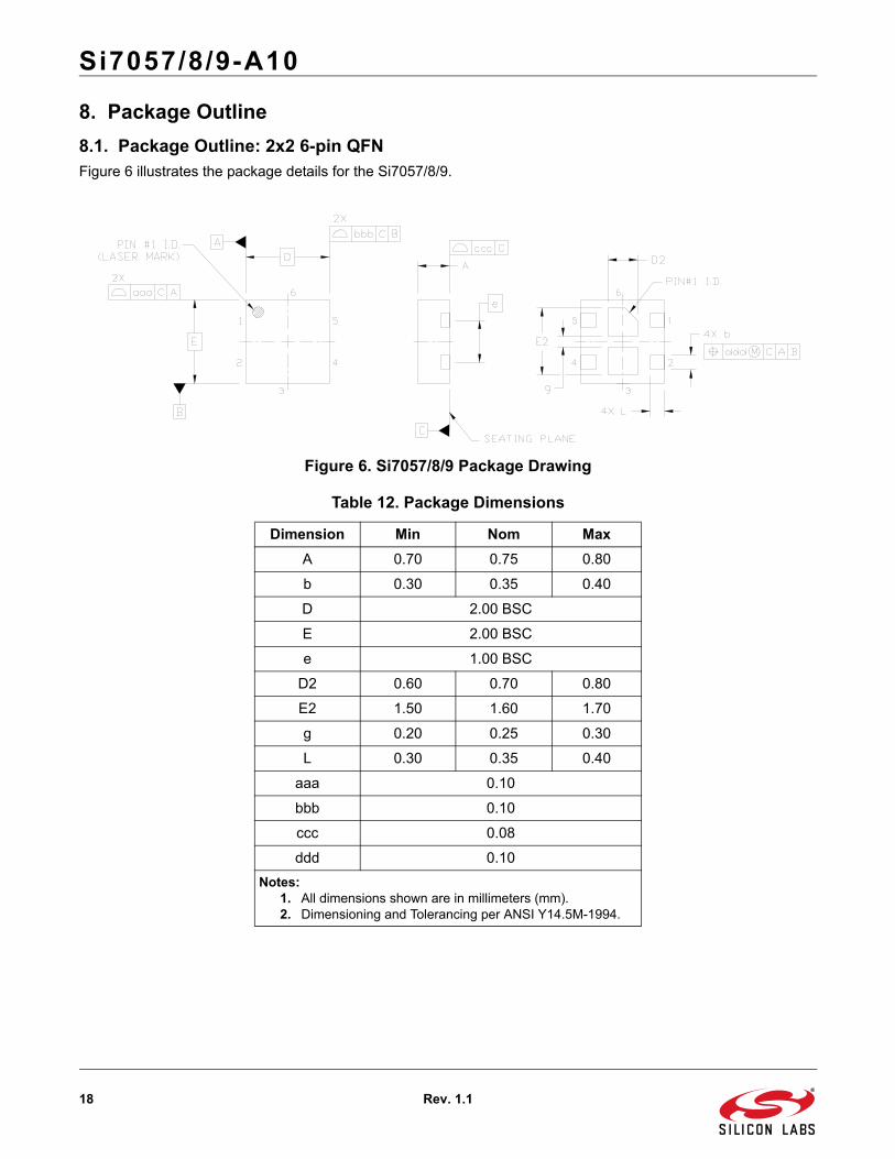
8. Package Outline 8.1. Package Outline: 2x2 6-pin QFNFigure 6 illustrates the package details for the Si7057/8/9.
Figure 6. Si7057/8/9 Package Drawing
Table 12. Package Dimensions
Dimension Min Nom MaxA 0.70 0.75 0.80
b 0.30 0.35 0.40
D 2.00 BSC
E 2.00 BSC
e 1.00 BSC
D2 0.60 0.70 0.80
E2 1.50 1.60 1.70
g 0.20 0.25 0.30
L 0.30 0.35 0.40
aaa 0.10
bbb 0.10
ccc 0.08
ddd 0.10
Notes:1. All dimensions shown are in millimeters (mm).2. Dimensioning and Tolerancing per ANSI Y14.5M-1994.

Si7057/8/9-A10
Rev. 1.1 19
9. PCB Land Pattern and Solder Mask Design
Figure 7. PCB Land Pattern Dimensions
Table 13. PCB Land Pattern Dimensions
Symbol mmC1 2.00
E1 1.00
E2 0.90
X1 0.40
Y1 0.75
Z 0.80
Notes:General
1. All dimensions shown are in millimeters (mm).2. This Land Pattern Design is based on the IPC-7351 guidelines.3. All dimensions shown are at Maximum Material Condition (MMC). Least Material
Condition (LMC) is calculated based on a Fabrication Allowance of 0.05 mm.Solder Mask Design
4. All metal pads are to be non-solder mask defined (NSMD). Clearance between the solder mask and the metal pad is to be 60 µm minimum, all the way around the pad.
Stencil Design5. A stainless steel, laser-cut and electropolished stencil with trapezoidal walls should
be used to assure good solder paste release.6. The stencil thickness should be 0.125 mm (5 mils).7. The ratio of stencil aperture to land pad size should be 1:1 for all pads.
Card Assembly8. A No-Clean, Type-3 solder paste is recommended.9. The recommended card reflow profile is per the JEDEC/IPC J-STD-020 specification
for Small Body Components.

Si7057/8/9-A10
20 Rev. 1.1
10. Top Marking10.1. Si7057/8/9 Top Marking
10.2. Top Marking Explanation
Mark Method: Laser
Font Size: 0.40 mm
Line 1 Marking: 705 = Device Code
Line 2 Marking: TTTT = Manufacturing Trace Code Digits 1–4
Line 3 Marking: Circle = 0.35 mm Diameter

Si7057/8/9-A10
Rev. 1.1 21
11. Additional Reference ResourcesAN607: Si70xx Humidity and Temperature Sensor Designer’s Guide
AN1026: Si70xx Temperature Sensor Designer's Guide

Si7057/8/9-A10
22 Rev. 1.1
DOCUMENT CHANGE LIST
Revision 0.9 to Revision 1.0 Clarified Features list on page 1.
Revision 1.0 to Revision 1.1April 18, 2017
Changed Si7057 max inaccuracy spec to 0.35 C
(was 0.2 C).
Updated Figure 2 and Figure 3.

http://www.silabs.com
Silicon Laboratories Inc.400 West Cesar ChavezAustin, TX 78701USA
Smart. Connected. Energy-Friendly.
Productswww.silabs.com/products
Qualitywww.silabs.com/quality
Support and Communitycommunity.silabs.com
DisclaimerSilicon Labs intends to provide customers with the latest, accurate, and in-depth documentation of all peripherals and modules available for system and software implementers using or intending to use the Silicon Labs products. Characterization data, available modules and peripherals, memory sizes and memory addresses refer to each specific device, and "Typical" parameters provided can and do vary in different applications. Application examples described herein are for illustrative purposes only. Silicon Labs reserves the right to make changes without further notice and limitation to product information, specifications, and descriptions herein, and does not give warranties as to the accuracy or completeness of the included information. Silicon Labs shall have no liability for the consequences of use of the information supplied herein. This document does not imply or express copyright licenses granted hereunder to design or fabricate any integrated circuits. The products are not designed or authorized to be used within any Life Support System without the specific written consent of Silicon Labs. A "Life Support System" is any product or system intended to support or sustain life and/or health, which, if it fails, can be reasonably expected to result in significant personal injury or death. Silicon Labs products are not designed or authorized for military applications. Silicon Labs products shall under no circumstances be used in weapons of mass destruction including (but not limited to) nuclear, biological or chemical weapons, or missiles capable of delivering such weapons.
Trademark InformationSilicon Laboratories Inc.® , Silicon Laboratories®, Silicon Labs®, SiLabs® and the Silicon Labs logo®, Bluegiga®, Bluegiga Logo®, Clockbuilder®, CMEMS®, DSPLL®, EFM®, EFM32®, EFR, Ember®, Energy Micro, Energy Micro logo and combinations thereof, "the world’s most energy friendly microcontrollers", Ember®, EZLink®, EZRadio®, EZRadioPRO®, Gecko®, ISOmodem®, Precision32®, ProSLIC®, Simplicity Studio®, SiPHY®, Telegesis, the Telegesis Logo®, USBXpress® and others are trademarks or registered trademarks of Silicon Labs. ARM, CORTEX, Cortex-M3 and THUMB are trademarks or registered trademarks of ARM Holdings. Keil is a registered trademark of ARM Limited. All other products or brand names mentioned herein are trademarks of their respective holders.