single-event effects of space and atmospheric …
TRANSCRIPT

DEPARTMENT OF PHYSICS, UNIVERSITY OF JYVÄSKYLÄ
LIRMM, UNIVERSITY OF MONTPELLIER/CNRS
RESEARCH REPORT No. 10/2017
SINGLE-EVENT EFFECTS OF SPACE AND ATMOSPHERIC RADIATION
ON MEMORY COMPONENTS
by
Alexandre Louis BOSSER
Academic Dissertation for the Degree of
Doctor of Philosophy
To be presented, by permission of the Faculty of Mathematics and Science of the University of Jyväskylä
and the President of the University of Montpellier, for public examination in Auditorium FYS 1 of the
University of Jyväskylä on December 20th, 2017 at 12 noon.
Jyväskylä, Finland
2017

2
Alexandre Louis Bosser, 1991-
Single-event effects of space and atmospheric radiation on memory components
Jyväskylä: University of Jyväskylä, 2017, 98 pages
Research report No. 10/2017, Department of Physics, University of Jyväskylä
ISSN 0075-465X; 10/2017
ISBN paper copy: 978-951-39-7311-7
ISBN electronic: 978-951-39-7312-4

3
Preface
I would like to express my deepest gratitude to my supervisors, Prof. Ari Virtanen, Dr Luigi Dilillo and Dr
Arto Javanainen, who showed great dedication at their task and were always available for fruitful
discussions, useful advice and support; I know that adequate supervision and good morale are key to the
success of doctoral studies. I was also fortunate to be given every possible opportunity to present my
research in international conferences, which greatly improved my visibility and my expertise. I am very
thankful for the exceptional work environment you have provided for me.
I would also like to thank my colleagues at RADEF and LIRMM, for the friendly work atmosphere and the
support they offered. In particular, I want to acknowledge the major contribution of Dr Viyas Gupta, who
started his PhD at LIRMM at the same time as I did; Viyas and I worked together on the topics presented
in this manuscript, preparing and carrying out the test campaigns, processing and discussing the data, and
writing the publications. It was a real pleasure working with you, and I hope we will collaborate again in
the future!
I’m also grateful to my reviewers, Prof. Simone Gerardin and Prof. Ronald Schrimpf, and to my Opponent
Prof. Fernanda Lima Kastensmidt, for the work they have accomplished and the useful comments they
provided on my thesis on short notice. I would like to give special thanks to Prof. Lima Kastensmidt for
travelling all the way to Finland for my defense.
This research was supported in part by the European Space Agency (ESA/ESTEC Contracts
4000111630/14/NL/PA and 4000111085/14/NL/PA), the European Commission (EU-HORIZON-
2020/RIA/R2RAM, project ID 640073, 2015-2016) and the Academy of Finland under the Finnish Centre
of Excellence Programme 2012-2017 (Project 2513553, Nuclear- and Accelerator-Based Physics).
Finally, I would like to thank my family, my friends, and most importantly my fiancée Anni Herranen, who
were always there to support me and cheer me up when I needed it. Thank you for carrying me through
five long, cold, dark Finnish winters!
Alexandre

4
Abstract
Electronic memories are ubiquitous components in electronic systems: they are used to store data, and
can be found in all manner of industrial, automotive, aerospace, telecommunication and entertainment
systems. Memory technology has seen a constant evolution since the first practical dynamic Random-
Access Memories (dynamic RAMs) were created in the late 60's. The demand for ever-increasing
performance and capacity and decrease in power consumption was met thanks to a steady
miniaturization of the component features: modern memory devices include elements barely a few tens
of atomic layers thick and a few hundred of atomic layers wide.
The side effect of this constant miniaturization was an increase in the sensitivity of these devices to
radiation. Since the first radiation-induced single-event effects (SEEs) were identified in satellites in the
late 70’s [1] and particle-induced memory upsets were replicated in laboratory tests [2], radiation
hardness has been a concern for computer memory manufacturers and for systems designers as well. In
the early days, the need for data storage in radiation-rich environments, e.g. nuclear facilities, particle
accelerators and space, primarily for military use, created a market for radiation-hardened memory
components, capable of withstanding the effects of radiation ; however, this market dwindled with the
end of the Cold War and the loss of government interest [3]. In a matter of years, the shortage of available
radiation-hard components led system designers to turn to so-called Commercial Off-The-Shelf (COTS)
components, with the added benefit of higher performance at a lower cost.
Since COTS devices are not designed with radiation hardness in mind, each COTS component must be
assessed before it can be included in a system where reliability is important – a process known as
Radiation Hardness Assurance (RHA) [4]. This has led to the emergence of radiation testing as a standard
practice in the industry (and in the space industry in particular). Irradiation tests with particle accelerators
and radioactive sources are performed to estimate a component’s radiation-induced failure rate in a given
radiation environment, and thus its suitability for a given mission.
The present work focuses on SEE testing of memory components. It presents the requirements, difficulties
and shortcomings of radiation testing, and proposes methods for radiation test data processing; the
detection and study of failure modes is used to gain insight on the tested components. This study is based
on data obtained over four years on several irradiation campaigns, where memory devices of different
technologies (static RAMs, ferroelectric RAM, magnetoresistive RAM, and flash) were irradiated with
proton, heavy-ion, neutron and muon beams. The yielded data also supported the development of
MTCube, a CubeSat picosatellite developed jointly by the Centre Spatial Universitaire (CSU) and LIRMM in
Montpellier, whose mission is to carry out in-flight testing on the same memory devices. The underlying
concepts regarding radiation, radiation environments, radiation-matter interactions, memory component
architecture and radiation testing are introduced in the first chapters.
Keywords: Radiation effects, memory, COTS, RAM, SRAM, FRAM, MRAM, flash, single-event effect,
radiation testing

5
Résumé
Les composants mémoires sont omniprésents en électronique : ils sont utilisés pour stocker des données,
et sont présents dans tous les champs d’application - industriel, automobile, aérospatial, grand public et
télécommunications, entre autres. Les technologies mémoires ont connu une évolution continue depuis
la création de la première mémoire vive statique (Static Random-Access Memory, SRAM) à la fin des
années 60. Les besoins toujours plus importants en termes de performance, de capacité et d’économie
d’énergie poussent à une miniaturisation constante de ces composants : les mémoires modernes
contiennent des circuits dont certaines dimensions sont de l’ordre du nanomètre.
L’un des inconvénients de cette miniaturisation fut un accroissement de la sensibilité de ces composants
aux radiations. Depuis la détection des premiers effets singuliers (Single-Event Effects, SEE) sur un satellite
à la fin des années 70 [1], et la reproduction du phénomène en laboratoire [2], les fabricants de
composants mémoires et les ingénieurs en électronique se sont intéressés au durcissement aux
radiations. Au début, les besoins en stockage pour applications civiles et militaires – comme le
développement d’accélérateurs de particules, de réacteurs nucléaires et d’engins spatiaux – créèrent un
marché pour les composants durcis aux radiations ; cependant, ce marché s’est considérablement réduit
avec la fin de la Guerre Froide et la perte d’intérêt des gouvernements [3]. En quelques années, les
ingénieurs durent se tourner vers des composants commerciaux (Commercial Off-The-Shelf Components,
COTS), ce qui permit au passage des gains en performance et une réduction des coûts.
Les composants COTS n’étant pas conçus pour résister aux radiations, chaque composant doit être évalué
avant d’être utilisé dans des systèmes dont la fiabilité est critique. Ce processus d’évaluation est appelé
Radiation Hardness Assurance (RHA) [4]. Les tests aux radiations des composants commerciaux sont
devenus une pratique standardisée (en particulier dans l’industrie aérospatiale). Ces composants sont
irradiés à l’aide d’accélérateurs de particules et de sources radioactives, afin d’évaluer leur sensibilité, de
prédire leur taux d’erreur dans un environnement radiatif donné, et ainsi de déterminer leur adéquation
pour une mission donnée.
Cette étude porte sur le test de composants mémoires aux effets singuliers. Les objectifs, difficultés et
limitations des tests aux radiations sont présentés, et des méthodes d’analyse de données sont
proposées ; l’identification et l’étude des modes de défaillance sont utilisées pour approfondir les
connaissances sur les composants testés. Cette étude est basée sur de nombreuses campagnes de test
aux radiations, effectuées sur une période de quatre ans, pendant lesquelles des mémoires de différentes
technologies – mémoires vives statiques (SRAM), ferroélectriques (FRAM), magnétorésistives (MRAM) et
mémoires flash – furent irradiées avec des faisceaux de muons, neutrons, protons et ions lourds. Les
données générées ont également servi au développement d’un CubeSat développé conjointement par le
LIRMM et le Centre Spatial Universitaire de Montpellier, MTCube, dont la mission est l’irradiation de ces
mêmes composants en milieu spatial. Les concepts sous-jacents liés aux radiations, aux environnements
radiatifs, à l’architecture des composants mémoires et aux tests aux radiations sont introduits dans les
premiers chapitres.
Mots-clés: Radiation effects, memory, COTS, RAM, SRAM, FRAM, MRAM, flash, single-event effect,
radiation testing

6
Author Alexandre Louis Bosser
Department of Physics, University of Jyväskylä
Jyväskylä, Finland
LIRMM, University of Montpellier/CNRS
Montpellier, France
email: [email protected]
Supervisors Professor Ari Virtanen
Department of Physics, University of Jyväskylä
Jyväskylä, Finland
Dr. Arto Javanainen
Department of Physics, University of Jyväskylä
Jyväskylä, Finland
School of Engineering, Vanderbilt University
Nashville, TN, USA
Dr. Luigi Dilillo
LIRMM, University of Montpellier/CNRS
Montpellier, France
Reviewers Professor Ronald Schrimpf
Institute for Space and Defense Electronics, Vanderbilt University
Nashville, TN, USA
Associate Professor Simone Gerardin
Department of Information Engineering, University of Padova
Padova, Italy
Opponent Professor Fernanda Lima Kastensmidt
Institute of Informatics, Federal University of Rio Grande do Sul
Porto Alegre, Brazil
7
List of peer-reviewed publications
This doctoral thesis is based in part on the following peer-reviewed publications:
I. A. L. Bosser, V. Gupta, A. Javanainen, G. Tsiligiannis, S. D. LaLumondiere, D. Brewe, V. Ferlet-Cavrois,
H. Puchner, H. Kettunen, T. Gil, F. Wrobel, F. Saigné, A. Virtanen and L. Dilillo, “Single-Event Effects in
the Peripheral Circuitry of a Commercial Ferroelectric Random-Access Memory” (presented at RADECS
2017, submitted for publication in IEEE Transactions on Nuclear Science)
Contribution: the author had a major role in the experiment’s software and hardware
development, took part in the test campaigns, and did most of the data processing and writing.
II. A. Bosser, V. Gupta, G. Tsiligiannis, A. Javanainen, H. Kettunen, H. Puchner, F. Saigné, A. Virtanen, F.
Wrobel and L. Dilillo, “Investigation on MCU Clustering Methodologies for Cross-Section Estimation
of RAMs”, in IEEE Transactions on Nuclear Science, Vol. 62, no. 6, pp.2620-2626, 2015.
Contribution: the author had a major role in the experiment’s software and hardware
development, took part in the test campaigns, and did most of the data processing and writing.
III. A. L. Bosser, V. Gupta, G. Tsiligiannis, C. Frost, A. Zadeh, J. Jaatinen, A. Javanainen, H. Puchner, F.
Saigné, A. Virtanen, F. Wrobel, and L. Dilillo, “Methodologies for the Statistical Analysis of Memory
Response to Radiation”, in IEEE Transactions on Nuclear Science, Vol. 63, no. 4, pp.2122-2128, 2016.
Contribution: the author had a major role in the experiment’s software and hardware
development, took part in the test campaigns, and did most of the data processing and writing.
IV. L. Dilillo, G. Tsiligiannis, V. Gupta, A. Bosser, F. Saigné and F. Wrobel, “Soft errors in commercial off-
the-shelf static random-access memories”, in Semiconductor Science and Technology, vol. 32, no.1,
2016
Contribution: the author had a major role in the experiment’s software and hardware
development, and took part in the test campaigns, data processing and writing.
V. V. Gupta, A. Bosser, G. Tsiligiannis, M. Rousselet, A. Zadeh, A. Javanainen, A. Virtanen, H. Puchner, F.
Saigné, F. Wrobel and L. Dilillo, "SEE on Different Layers of Stacked-SRAMs", in IEEE Transactions on
Nuclear Science, vol. 62, no. 6, pp. 2673-2678, 2015.
Contribution: the author had a major role in the experiment’s software and hardware
development, and took part in the test campaigns and writing.
VI. V. Gupta, A. Bosser, G. Tsiligiannis, A. Zadeh, A. Javanainen, A. Virtanen, H. Puchner, F. Saigné, F.
Wrobel and L. Dilillo, "Heavy-Ion Radiation Impact on a 4 Mb FRAM Under Different Test Modes and
Conditions," in IEEE Transactions on Nuclear Science, vol. 63, no. 4, pp. 2010-2015, Aug. 2016.
Contribution: the author had a major role in the experiment’s software and hardware
development, and took part in the test campaigns.
VII. G. Tsiligiannis, L. Dilillo, V. Gupta, A. Bosio, P. Girard, A. Virazel, H. Puchner, A. Bosser, A. Javanainen,
A. Virtanen, C. Frost, F. Wrobel, L. Dusseau, and F. Saigné, "Dynamic Test Methods for COTS SRAMs,"
in IEEE Transactions on Nuclear Science, vol. 61, no. 6, pp. 3095-3102, 2014.
Contribution: the author took part in the test campaigns.

8
Table of Contents Preface .......................................................................................................................................................... 3
Abstract ......................................................................................................................................................... 4
List of peer-reviewed publications................................................................................................................ 7
Chapter I – Radiation Environments ............................................................................................................. 9
A. Space radiation ............................................................................................................................. 9
B. Atmospheric radiation ................................................................................................................ 12
C. Artificial radiation sources .......................................................................................................... 14
Chapter II – Radiation-matter interactions ................................................................................................. 16
A. Photon-matter interactions ........................................................................................................ 16
B. Particle-matter interactions ....................................................................................................... 17
C. Consequences of irradiation ....................................................................................................... 19
D. Useful concepts for radiation testing ......................................................................................... 21
Chapter III – Memory devices ..................................................................................................................... 24
A. General principles ....................................................................................................................... 24
B. Memory cell technologies .......................................................................................................... 27
C. Device manufacturing ................................................................................................................. 29
Chapter IV – Radiation effects on memory components ........................................................................... 32
A. Total Ionizing Dose (TID) effects ................................................................................................. 32
B. Single-Event Effects (SEEs) .......................................................................................................... 34
Chapter V – Radiation testing of memory components ............................................................................. 41
A. Radiation Hardness Assurance ................................................................................................... 41
B. Testing standards and methodologies ....................................................................................... 42
C. Concepts and metrics for radiation testing ................................................................................ 43
D. Algorithms for memory testing .................................................................................................. 44
Chapter VI – Experimental setup ................................................................................................................ 46
A. Test setups .................................................................................................................................. 46
B. Data processing .......................................................................................................................... 51
Chapter VII – Test results and discoveries .................................................................................................. 54
A. Clustering of bit errors in a 90 nm SRAM ................................................................................... 54
B. Statistical analysis of the radiation response of a 65 nm SRAM ................................................ 57
C. Muon-induced Single-Event Upsets in a 65 nm SRAM ............................................................... 64
D. Failure mode analysis of an FRAM.............................................................................................. 69
E. Effects of heavy-ion radiation on a Single-Level Cell NAND flash memory ................................ 80
F. Single-Event Latch-ups in an MRAM ........................................................................................... 85
Chapter VIII – Summary .............................................................................................................................. 89
References .................................................................................................................................................. 90
Annexes ....................................................................................................................................................... 99
9
Chapter I – Radiation Environments
Radiation is a term used to designate the emission or transmission of energy, in the form of waves or
particles. Although it can sometimes be used to designate acoustic radiation (the propagation of sound
waves) or even gravitational radiation (the propagation of gravitational waves), its most commonly
accepted meaning (and the one which will be retained in the present thesis) restricts it to electromagnetic
radiation and particle radiation.
Electromagnetic radiation is the propagation of electromagnetic waves: this includes radio waves and
microwaves, infrared, visible and UV light, X-rays and γ-rays. Particle radiation designates the propagation
of energetic (ie. high-speed) particles, which includes (among other particles) electrons, neutrons, protons
and heavier ions. These particles may or may not carry electric charge.
A distinction can be made between non-ionizing radiation and ionizing radiation, which has the power to
ionize matter (remove electrons from target atoms). However, the boundary between the two is not
sharply defined, because different target materials ionize at different energies.
The type, energy and flux of radiation which can be encountered at a given place is referred to as a
radiation environment. In the following sections, various typical radiation environments will be described.
A. Space radiation
1) Interplanetary radiation environment The main source of interplanetary radiation is the Sun, with the higher-energy tail of the spectrum coming
from distant stars and supernovae.
The Sun emits electromagnetic radiation across most of the electromagnetic spectrum; while it does emit
gamma rays, X-rays, microwaves and radio waves, most of its power output is emitted at wavelengths
between 100 nm and 1 mm (which includes ultraviolet, visible and infrared light).
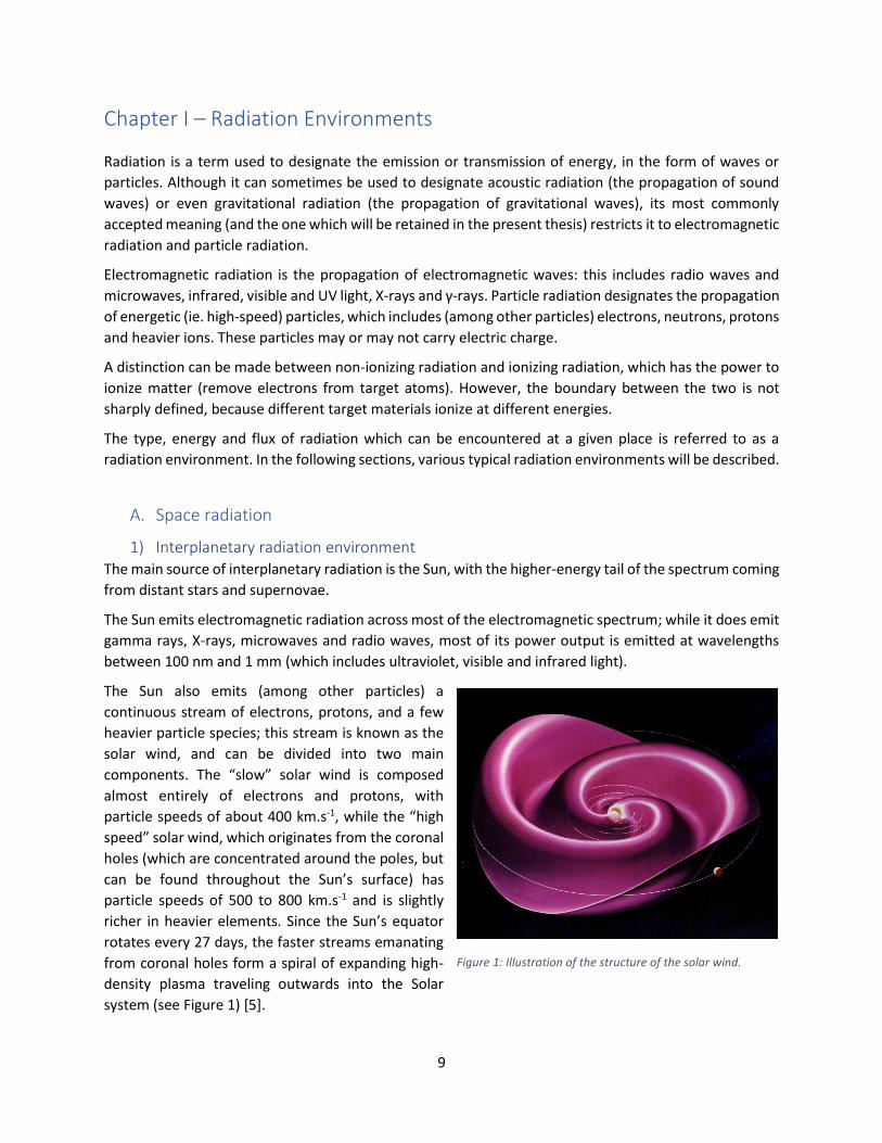
The Sun also emits (among other particles) a
continuous stream of electrons, protons, and a few
heavier particle species; this stream is known as the
solar wind, and can be divided into two main
components. The “slow” solar wind is composed
almost entirely of electrons and protons, with
particle speeds of about 400 km.s-1, while the “high
speed” solar wind, which originates from the coronal
holes (which are concentrated around the poles, but
can be found throughout the Sun’s surface) has
particle speeds of 500 to 800 km.s-1 and is slightly
richer in heavier elements. Since the Sun’s equator
rotates every 27 days, the faster streams emanating
from coronal holes form a spiral of expanding high-
density plasma traveling outwards into the Solar
system (see Figure 1) [5].
Figure 1: Illustration of the structure of the solar wind.
10
In addition to the continuous solar wind, the Sun occasionally emits massive bursts of plasma, in events
known as solar flares and Coronal Mass Ejections (CME). These events originate in regions where the Sun’s
magnetic field lines bundle up in to helical structures known as flux ropes [6]. The ejected plasma is mostly
made up of protons and electrons, with a small fraction of helium ions (alpha particles) and trace amounts
of heavier nuclei, and travels at speeds around 100 km.s-1 to around 3000 km.s-1 [7]. As it travels through
interplanetary space, it interacts with the slower solar wind plasma, creating high-density particle
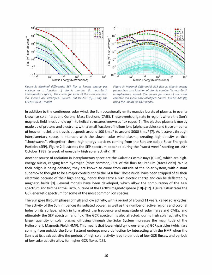
“shockwaves”. Altogether, these high-energy particles coming from the Sun are called Solar Energetic
Particles (SEP). Figure 2 illustrates the SEP spectrum obtained during the “worst week” starting on 19th
October 1989 (a week of unusually high solar activity) [8].
Another source of radiation in interplanetary space are the Galactic Cosmic Rays (GCRs), which are high-
energy nuclei, ranging from hydrogen (most common, 89% of the flux) to uranium (traces only). While
their origin is being debated, they are known to come from outside of the Solar System, with distant
supernovae thought to be a major contributor to the GCR flux. These nuclei have been stripped of all their
electrons because of their high energy, hence they carry a high electric charge and can be deflected by
magnetic fields [9]. Several models have been developed, which allow the computation of the GCR
spectrum and flux near the Earth, outside of the Earth’s magnetosphere [10]–[12]. Figure 3 illustrates the
GCR energetic spectrum for some of the most common ion species.
The Sun goes through phases of high and low activity, with a period of around 11 years, called solar cycles.
The activity of the Sun influences its radiated power, as well as the number of active regions and coronal
holes on its surface, which in turn affect the frequency and magnitude of solar flares and CMEs, and
ultimately the SEP spectrum and flux. The GCR spectrum is also affected: during high solar activity, the
larger quantity of solar plasma diffusing through the Solar System increases the magnitude of the
Heliospheric Magnetic Field (HMF). This means that lower-rigidity (lower-energy) GCR particles (which are
coming from outside the Solar System) undergo more deflection by interacting with the HMF when the
Sun is at its peak activity: the periods of high solar activity lead to periods of low GCR fluxes, and periods
of low solar activity allow for higher GCR fluxes [13].
Figure 2: Maximal differential SEP flux vs kinetic energy per nucleon as a function of atomic number (in near-Earth interplanetary space). The curves for some of the most common ion species are identified. Source: CREME-MC [8], using the CREME 96 SEP model.
Figure 3: Maximal differential GCR flux vs. kinetic energy per nucleon as a function of atomic number (in near-Earth interplanetary space). The curves for some of the most common ion species are identified. Source: CREME-MC [8], using the CREME 96 GCR model.

11
2) Near-Earth radiation environment The Earth generates a dipole-like magnetic field, with
its centre slightly offset from the Earth’s centre, and
tilted about 11° with respect to its rotational axis.
The origin of this magnetic field is thought to be the
motion of electrically conductive liquid iron alloys in
the Earth’s outer core, driven by thermal convection
and Coriolis forces caused by the rotation of the
Earth – an origin theory known as the “dynamo
theory” [14]. As they encounter the Earth’s magnetic
field, charged particles (such as solar wind plasma,
SEPs and GCRs) are deflected by a force known as the
Lorentz force, which is proportional to their speed
and to the magnitude of the magnetic field. This
phenomenon has a two-fold impact on the near-
Earth radiation environment.
The particles of low magnetic rigidity1 (i.e. GCRs and high-energy SEP) can be deflected away from the
Earth: this geomagnetic shielding effect prevents them from reaching areas where the geomagnetic field
is stronger (at low altitudes and high latitudes). Figure 4 illustrates the effect of the geomagnetic shielding
on the particle spectrum as a function of magnetic latitude and ion species (which, for fully-stripped GCRs,
determines their rigidity).
The trajectories of the lowest-energy, least rigid
particles (protons and electrons) are bent so much
that they can be trapped in a broad region,
extending from a few hundred kilometres to about
60.000 km of altitude, called the Van Allen radiation
belts (Figure 5). The belts have a roughly toroidal
shape, centered around the Earth’s magnetic centre
and aligned with its magnetic equator. Inside the
belts, individual trapped particles drift around the
Earth, depending on their electrical charge
(eastward for electrons, and westward for protons);
additionally, they move along a helicoidal path around the Earth’s magnetic field lines, “bouncing” back
and forth between the two magnetic poles [15]-p.22. As the magnetic field lines get closer to the Earth
near the poles, these trapped particles may interact with atoms in the upper atmosphere, resulting in the
generation of low-energy, “cold” plasma. This phenomenon is also the source of auroral displays.
The particles trapped in the Earth’s magnetic field tend to concentrate at different altitudes depending
on their mass and velocity. Traditionally, the Van Allen belts are considered to consist of a smaller inner
belt, and a larger outer belt. The inner belt is made of protons (at energies up to 400 MeV) and electrons
(at energies up to 5 MeV), while the outer belt is exclusively made up of electrons (at energies up to 7
1 Magnetic rigidity is a quantity amounting to a particle’s momentum divided by its electrical charge, which specifies its curvature radius when subjected to a given magnetic field.
Figure 5: Illustration of the structure of the Van Allen radiation belts. Image from the public domain (credit: NASA)
Figure 4: Effect of the geomagnetic shielding on the cosmic ray spectrum as a function of magnetic latitude and ion species. The spectrum is calculated behind 2,54 mm of aluminium. Data source: Petersen et al. [15]-p.35

12
MeV) [16]. However, the structure and particle fluxes of these radiation belts are influenced by solar
activity, and can change dramatically when plasma from a solar flare or CME encounters the Earth [17].
Several models have been developed over the years to describe the characteristics of the Earth’s trapped
radiation field, a recent example being the AE9/AP9/SPM model [18].
Because the centre of the Earth’s magnetosphere is slightly offset with the centre of the Earth, the lower
boundary of the inner belt comes closer to the upper atmosphere (from 1000 km down to about 200 km
of altitude) in a region roughly located above South America and the southern Atlantic Ocean. This region
of higher radiation levels at low altitudes, called the South Atlantic Anomaly (SAA), represents a threat to
electronic devices; in Low Earth Orbit (LEO), the SAA accounts for virtually all of the proton fluence (at
energies above 30 MeV) received by a spacecraft [15]-p.44.
Other planets than the Earth (most notably Jupiter and Saturn) possess a magnetic field strong enough to
interact significantly with charged energetic particles; phenomena and structures similar to these
described in this section can be found around these planets.
B. Atmospheric radiation
As mentioned in the previous section, the
geomagnetic field can deflect low-rigidity Earth-
bound charged particles. However, with the
right angle of incidence and high enough rigidity
(high enough energy), charged particles may
penetrate the Earth’s magnetic field and enter
the upper atmosphere. These high-energy ions
eventually undergo nuclear interactions with
the atmosphere, generating high-energy
reaction products (e.g. muons, pions, gamma
photons, lighter nuclei…) which in turn trigger
nuclear reactions with the atmosphere (or decay
into other products). After several steps, a
cascade of secondary particles has taken form,
called a “cosmic ray shower”. These cosmic ray
showers are more abundant at higher magnetic
latitudes, because the geomagnetic shielding
effect is weaker near the poles.
Nuclear interactions degrade the cosmic ray
spectrum until about 15 km of altitude, at which
point virtually all primary cosmic rays have
interacted and turned into secondary particles
(although the proton spectrum remains
significant) [19]. These secondary particles,
which carry part of the original cosmic ray momentum, generally follow a downwards trajectory, losing
energy through nuclear scattering, electronic stopping and light emission, until they decay into other
particles, are captured, or come to a rest in matter. Figure 6 illustrates the vertical flux of cosmic ray
Figure 6: Vertical fluxes of atmospheric cosmic ray shower particles with E > 1 GeV. The data points represent different measurements for negative muon flux. Source: Patrignani et al. [20].

13
shower particles in the atmosphere [20]. Among these secondary particles, neutrons and
muons/antimuons are the most numerous below 20 km of altitude; indeed, their lifetime spans more than
a few microseconds, and they are not easily stopped by air. This makes them the most significant threat
to electronic component reliability.
1) Atmospheric neutrons Atmospheric neutrons are one of the types of secondary particles which are produced in cosmic ray
showers. Neutron production starts at very high altitudes (> 150 km), and as the atmosphere gets denser
and the cosmic ray interactions increase, so does the neutron flux, until it reaches a peak called the Pfotzer
maximum around 20 km of altitude. Considering only neutrons with an energy > 1 MeV, the flux at the
Pfotzer maximum is at least 3.5*10-1 neutrons.cm-2.s-1 at 42° magnetic latitude [21]. Below 20 km, the
thickening of the atmosphere effectively reduces the flux: at ground level, it is two to three orders of
magnitude lower than its peak value. Since the atmospheric neutron flux is a consequence of the incident
high-energy cosmic ray flux, it is strongly influenced by geomagnetic shielding: the neutron flux can be six
times higher at the poles than at the equator [22].
Eventually, after several collisions causing gradual energy loss, if they are not captured by encountered
nuclei, these neutrons reach thermal equilibrium. Their kinetic energy stabilizes around an energy of
about 0.025 eV, which is the most probable energy for a free particle at room temperature. These thermal
neutrons generally interact more easily with matter [23], in particular with elements such as cadmium-
113 and boron-10; hence, electronic parts containing these elements (for example, boron-10 in
borophosphosilicate glass insulating layers) are more likely to be disturbed by thermalized neutrons.
2) Atmospheric muons and antimuons Muons are one of the decay product of pions, which are very short-lived subatomic particles released in
high-energy nuclear collisions such as those taking place in a cosmic ray shower. Muons (and their
antiparticles, antimuons) are unstable elementary particles, with a half-life of 1.52 μs. They eventually
decay in an electron (or positron) and two neutrinos. They carry one negative elementary charge (or, in
the case of antimuons, one positive charge) and have a mass about 207 times greater than that of an
electron (or about 1/9th the mass of a proton).
Cosmic ray showers release large amounts of relativistic muons: they undergo a significant time dilation
effect because of their high velocities, which allows them to live long enough to travel for several
kilometres. Additionally, at these high energies (atmospheric muons generally have energies > 1 GeV)
muons only lose energy at a very low rate (as low as 2*10-3 MeV.cm-2.mg-1 [24]), which gives them a high
penetration capacity. Muons can go through the atmosphere, and may even travel several kilometres
underground before decaying or stopping.
3) Naturally-occurring radionuclides Part of the natural radiation background at ground level originates from naturally occurring radionuclides.
Among these elements, radon-222 is a major contributor. It is a short-lived radioactive noble gas, which
is continually produced as one of elements in the radium, uranium and thorium decay chains. Being a very
dense gas, it tends to accumulate in caves, and poorly-ventilated buildings and cellars near bedrock. It
decays into polonium-218 by emitting a 5.59 MeV alpha particle; the range of these particles in common
plastics and ceramics doesn’t exceed a few micrometres, hence these are not a concern for most packaged
electronics. However, in some specific cases where electronics operate with bare dies, the alpha radiation
from naturally-occurring radon can cause malfunctions and must be considered.

14
Naturally-occurring radionuclides can also contaminate the materials used in component manufacturing
(e.g. silicon, lead…) and packaging at part-per-trillion to part-per-million levels. When such contaminants
decay, they release radiation which can be detrimental to the component’s reliability. The presence of
alpha-emitting contaminants, such as uranium-238, thorium-232, and their decay products, was already
a concern in the late 70’s [25] and is still a reliability issue to this day [26].
C. Artificial radiation sources
A wide range of technical scenarios require electronic components to operate in radiative environment
where the main radiation source is artificial. These radiation sources can be antennae, lasers, man-made
radioactive sources (radionuclides), particle accelerators, nuclear reactors, and nuclear weapons. These
artificial sources cover a very wide range of particle species, energy and flux levels, with a wide range of
possible consequences on electronic systems.
1) Man-made radioactive sources Certain industrial applications require the use of radiation sources. One good example is the use of
gamma-ray sterilization units, where the gamma rays produced by the decay of a mass of cobalt-60 are
used to sterilize a wide variety of pharmaceutical, agricultural and food products, for the purpose of
disinfection, shelf life extension, or sprout inhibition [27]. Another example is the use of gamma-ray, x-
ray and, more rarely, neutron imagers for cargo, luggage, and passenger inspection at transit centres,
harbours and airports [28].
In the electronics industry, automated X-ray inspection (AXI) of printed circuit boards (PCBs) has become
a standard procedure for quality control, in particular to inspect the quality of solder connections. AXI
techniques allow the observation of solder joints which are not directly visible, such as those under ball
grid array (BGA) packages [29]. This raises the concern of the sensitivity of these components to
accumulated dose.
2) Particle accelerators and nuclear power plants Particle accelerators are facilities where charged particles are accelerated using electric and magnetic
fields. The resulting particle beams are valuable tools to perform fundamental and applied research in
many scientific disciplines. They represent a serious radiation hazard: the largest particle accelerators are
generally designed to reach high particle fluxes and energies, and generate particle beams which can
activate (generate radioactivity in) the materials they touch. High-energy ions straying away from the
beam will generate so-called “hadronic cascades” of secondary particles such as protons, neutrons, pions
and kaons akin to cosmic ray showers. Since such extremely complex machines require complex electronic
control systems to operate, the effects of stray radiation on these systems are a major concern and a
subject of investigation [30]. Small accelerators are also used for medical applications: x-rays are used in
radiology to image internal organs, and x-rays, gamma rays, and proton or carbon beams are used to treat
cancer (radiation oncology). The devices used for these applications may generate high enough fluxes of
secondary radiation [31] to pose a threat to surrounding electronic devices.
Nuclear power plant operation also generates a considerable amount of radiation – gamma rays, X-rays,
protons, neutrons, alpha particles and electrons. One of the main challenges of nuclear power plant

15
radiation safety is to shield equipment (and personnel) from gamma and neutron radiation, because they
are highly penetrating.
3) Nuclear weapons Upon detonation, nuclear weapons release heavy radioactive particles known as nuclear fallout, as well
as a burst of high-energy gamma rays and neutrons. This gamma-ray burst generates a wave of scattered
Compton electrons as the gamma rays interact with the air; these energetic electrons are deflected by the
geomagnetic field, which leads to the emission of synchrotron radiation in the general direction of the
electrons’ trajectories. Since the initial gamma burst propagates at the speed of light, the synchrotron
radiation from the secondary Compton electrons adds coherently, leading to the formation of an
electromagnetic pulse (EMP). These pulses are capable of inducing very high voltages in ground-level
conductors [32], which makes EMPs a major concern for military electronics designers [33].

16
Chapter II – Radiation-matter interactions
When radiation encounters matter, several different interaction processes may ensue, which depend on
the encountered material, and on the energy and type of the incoming radiation. Two broad categories
can be defined: ionizing and non-ionizing radiation. In this chapter, the physical processes which are the
most relevant for the study of radiation effects on electronics will be introduced. In the following chapter,
the material encountered by the radiation will be designed as the “target material” or “target”.
The concept of cross-section is commonly used to quantify the probability of a certain type of radiation-
matter interaction to occur. The cross-section of a reaction represents the area (as measured on a plane
orthogonal to their relative motion) within which these particles must meet for the reaction to occur: the
larger the cross-section, the more likely the reaction is.
A. Photon-matter interactions
Photons can interact with matter via several physical processes. In the scope of this study, we will only
consider the processes by which the interaction leads to an energy loss for the photon:
• the photoelectric effect, where an electron captures a photon with an energy higher than its own
binding energy, and as a result is ejected from its atom;
• Compton scattering, the inelastic interaction between a photon and an electron of a target atom
– part of the energy of the photon being transferred to the ejected electron;
• pair production, a process whereby a high-energy photon interacts with the nucleus of a target
atom, and is converted into an electron-positron pair [34];
• triplet production, a process whereby a high-energy photon interacts with an electron of a target
atom and is converted into an electron-positron pair, knocking off the target electron in the
process [34].
For these processes to take place, the
incident photon must carry an energy
higher or equal to the first ionization energy
of the target atom. The photoelectric effect
is the dominant interaction mechanism for
low-energy photons (a few eV up to a few
keV), while pair and triplet production must
involve photons carrying an energy superior
to the rest mass of an electron and a
positron (1.022 MeV). The predominance of
these mechanisms in photon absorption in
a lead target is plotted on Figure 7 [35].
As a result of these interactions, part or all
of the initial photon energy is transferred to
a recoiling electron (or positron) which then deposits this energy in the surrounding material. This is done
via other physical processes, which are described in the following section.
Figure 7: Predominance of photoelectric, Compton and pair production interactions in a lead target as a function of incident photon energy. Source: Joshua Hikes, using the ENDF/B-VII.0 database, under CC BY-SA 3.0 license.

17
B. Particle-matter interactions
Particle radiation can interact with matter via several physical processes, depending on the type of
particle. The most relevant for the scope of this study are electronic stopping, elastic and inelastic nuclear
interactions, and capture. This excludes radiative losses, which are the dominant energy loss mechanism
for very high-energy particles.
1) Electronic stopping Coulomb’s law states that charged particles exert a force on each other, which is proportional to the
magnitude of their charges and inversely proportional to the square of the distance between them.
Particles carrying charges of the same sign will repel each other, while opposite charges will attract each
other. As a charged particle travels through matter, the electrons of the surrounding atoms exert an
electrostatic force on the travelling particle and slow it down. This phenomenon is called electronic
stopping. In return, the charged particle will exert an electrostatic force on the surrounding electrons,
which can be sufficient to remove them from their atoms – thus leaving an ionized track along its
trajectory.
The maximum amount of energy which can be transferred to an electron in a single non-relativistic
collision, Wmax, is given by the following formula:
𝑊𝑚𝑎𝑥 =2𝑚𝑒𝑣2
1 + (𝑚𝑒𝑀 )
2 Equation 1
In this formula, 𝑚𝑒 is the mass of an electron, 𝑐 is the speed of light, 𝑣 the velocity of the incident particle,
and 𝑀 the mass of the incident particle. In the case of low-energy charged ions, 𝑚𝑒 ≪ 𝑀 , so we can make
the approximation 𝑊𝑚𝑎𝑥 = 2𝑚𝑒𝑣2.
The average rate of energy loss through electronic stopping for the incident particle is given by the
following formula [36]:
−𝑑𝐸
𝑑𝑥 𝑒𝑙𝑒𝑐=
1
4𝜋𝜖02
𝑍12𝑒4
𝑚𝑒𝑣2𝑁𝑍2𝐿 Equation 2
with 𝑍1 the charge number of the incident particle, 𝑍2 the atomic number of the target atoms, N the
atomic density of the target material, 𝜀0 the vacuum permittivity, 𝑒 the elementary charge, and L is a
dimensionless quantity called the stopping number. Different theories give different expressions for the
value of L. Bohr’s stopping theory gives the following expression:
𝐿𝐵𝑜ℎ𝑟 =1
2ln [1 + (𝐶
𝑚𝑒𝑣3
𝑍1𝐼𝛼𝑐)
2
] Equation 3
In this equation, 𝐼 = ℏ𝜔0 is the material-dependent mean excitation energy, with ℏ the Planck constant
and 𝜔0 the associated photon angular frequency, and 𝛼 is the fine-structure constant. This equation has
been introduced in Ref. [37], and is based on Ref. [38].
Bethe’s stopping theory gives a different expression for the stopping number:

18
𝐿𝐵𝑒𝑡ℎ𝑒 = ln2𝑚𝑒𝑣2
𝐼
Equation 4
This formula, which was introduced in Refs. [37] and [39], is only valid when 2𝑚𝑒𝑣2 ≫ 𝐼.
These formulae demonstrate the dependency of the electronic stopping force on the charge number of
the incoming particle (i.e. its atomic number if it is an ion), its velocity, and the atomic number and mass
of the target material. The equation shows that heavy particles (𝑀 ≫ 𝑚𝑒) travelling at the same velocity
and with a similar charge 𝑍1 (e.g. an antimuon and a proton) will experience the same electronic stopping
power.
2) Nuclear stopping In addition to interacting with the electrons of the target
atoms, incoming ions may also pass near and interact with the
nuclei of the target atoms (see Figure 8). If the incident particle
energy is below the energy necessary to overcome the
Coulomb barrier2, the two particles will undergo elastic nuclear
scattering (also called Rutherford scattering). The incoming
particle will be deflected of an angle θ (which depends on the
impact parameter b, the electric charges of the incoming
particle and target nucleus, and their relative velocity) and
transfer part of its kinetic energy to the target atom; if this
energy transfer is larger than its lattice binding energy, the
target atom will be knocked free and will recoil. The differential
cross-section 𝑑𝜎 for an incident particle to be deflected into a
solid angle 𝑑𝛺 = 2𝜋 𝑠𝑖𝑛𝜃 𝑑𝜃 through nuclear scattering is
given by the following equation (Ref. [40]):
𝑑𝜎
𝑑𝛺= (
𝑧𝑍ℏ𝑐
4)
2
(𝛼
𝐸)
2 1
𝑠𝑖𝑛4 𝜃2
Equation 2
where 𝑧 and 𝑍 are the respective atomic numbers of the incident ion and target atom, ℏ is the Planck
constant and 𝛼 is the fine-structure constant. This cross-section increases with decreasing incident
particle energy 𝐸; this means that the scattering events are more common, hence that the average nuclear
stopping force is higher for lower-energy incident particles.
3) Nuclear reactions If the energy of an incident ion is equal to - or higher than - the Coulomb barrier (or if the incident particle
carries no charge, in the case of a neutron) and its trajectory brings it close enough to the nucleus of a
target atom, then nuclear reactions may take place. An ion may exchange energy, momentum, even
nucleons with the target nucleus; a neutron may scatter elastically or inelastically off the target nucleus,
or be captured. Inelastic reactions and neutron captures leave one or both nuclei in an excited state, which
2 The Coulomb barrier is the energy necessary to bring two nuclei from infinity to a distance r of each other, which
is small enough for the nuclei to undergo a nuclear reaction. Its formula is 𝑈𝑐𝑜𝑢𝑙 =1
4𝜋𝜀0
𝑞1𝑞2
𝑟 , with 𝜀0 the vacuum
permittivity, and 𝑞1 and 𝑞2 their respective charges.
Figure 8: Illustration of the elastic nuclear scattering at an angle θ of a positively-charged incoming particle. b is the impact parameter.

19
eventually undergo de-excitation via one or several possible modes, including gamma-ray emission, and
alpha and beta decay. The interaction can also lead to the release of reaction products (lighter nuclei and
neutrons) via nuclear fission, neutron evaporation and neutron spallation, or radioactive decay (if the
reaction products are unstable); these daughter particles can in turn generate follow-up nuclear reactions
and ionization in the target [41].
For charged ions, these processes are much more likely to take place at high incident particle energies,
because of the electrostatic forces which tend to separate the two nuclei. Conversely, for nuclear
reactions involving neutrons, the cross-section is heavily dependent on the target isotope and on the
energy of the incident neutron: at certain energies (called “resonant energies”) the cross-section may
exhibit narrow peaks of several orders of magnitude in amplitude [42]. Certain isotopes, such as boron-
10 and cadmium-113, have remarkably high low-energy (so-called “thermal”) neutron capture cross-
sections, which means that their presence in a target material, even in small quantities, can drastically
influence the amount of nuclear reactions which will take place in the target if it is exposed to thermal
neutrons. This can have consequences for electronic components, as will be discussed in the next
chapters.
4) Coming to rest, capture, annihilation After they have lost their kinetic energy to the surrounding material, ions come to a stop within the target.
Light ions (protons, alpha particles) may escape solid targets in gaseous form [43], but heavier ions will
remain in the target.
When they reach a sufficiently low velocity (comparable to that of the target atoms’ electrons), light
particles such as electrons and muons (μ-) may end up being captured by a nearby atom. Captured muons
rapidly decay to the lowest muonic orbital state, where they may either decay into an electron, neutrino
and antineutrino, or be captured by the nucleus. The nuclear capture leads to the fragmentation of the
nucleus, releasing recoiling heavy ions and light particles (neutrons, protons, α-particles, etc…) [44], [45].
Conversely, antimuons (μ+) may capture an electron from the target material and form an unstable
pseudoatom called muonium [46]. Eventually, antimuons, being unstable particles, undergo decay into a
positron, a neutrino and an antineutrino.
Positrons eventually encounter an electron, and the electron-positron pair annihilates, releasing a pair of
511 keV gamma ray photons.
C. Consequences of irradiation
1) Consequences of ionization As discussed previously, through different physical processes, much of the energy lost by the incident
particle eventually goes to ionizing (ripping electrons off) the atoms of the target material, either directly
via electronic stopping, or indirectly from electronic stopping of recoiling nuclei or nuclear reaction
products. The most energetic electrons set free in this manner, which can travel over significant distances,
are commonly referred to as “delta rays” in the literature.
Electrons and holes
The electrons which are ripped from their original atoms leave a hole behind – a position where an
electron could exist in a bound state. Since the ripped electrons do not participate in screening the charge

20
of the nuclei of their original atom, the holes they leave behind appear to carry a positive charge. Holes
can be filled by bound electrons from the nearby atoms, which in turn leave a hole behind; this
displacement of positively-charged electron holes can be studied by assimilating each hole to a virtual
particle, carrying one positive elemental electric charge. Free electrons (electrons present in the material,
which are not bound to an atom) and holes can annihilate each other in a process known as recombination
[47]. Ionizing radiation thus has the effect of creating electron-hole pairs, in excess of the naturally-
occurring equilibrium concentrations. Depending on the target material, this ionization may have different
consequences.
Effects of ionization on different materials
Electrical conductors naturally present large concentrations of “free” conduction electrons, so ionization
has virtually no impact; however, if a conductor is insulated from its surroundings, delta rays escaping the
conductor can lead to positive charge buildup.
In electrical insulators, free charge carrier concentrations are naturally extremely low, and so are charge
carrier mobilities (in particular hole mobility [48]). In the absence of an electric field, electron-hole pairs
created by ionizing radiation are likely to recombine. However, if an electric field is present in the
insulator, the electrons will be able to drift (and eventually be collected by a conductor) much faster than
the holes; additionally, holes are easily trapped in defects in oxides [49]. Over time, this leads to a buildup
of positive charge in the insulator, which will modify the electric field across the insulator and may disturb
nearby circuits. This category of effects, called Total Ionizing Dose (TID) effects, will be discussed in further
detail in a following chapter. With increasing temperature, the carrier mobility increases; trapped holes
are more likely to escape their trapping sites and drift out of the insulator, thereby partly neutralizing TID
effects – a phenomenon known as annealing.
In semiconductors, the creation of electron-hole pairs by radiation can have a wide range of
consequences, depending on the function of the target material. In off-state transistors and reverse-
biased diodes, the applied bias concentrates across a region of the semiconductor crystal, known as the
depletion region, which is devoid of free charge carriers. When a single particle strikes the depletion
region and generates charge carriers, the intense electric field separates the electron-hole pairs; the holes
are collected at the negative electrode while the electrons are collected at the positive electrode, which
results in the generation of a current pulse. The occurrence of these current pulses through off-state
components can lead to a category of errors called Single-Event Effects (SEE) [50], which will be discussed
in further detail in a following chapter.
2) Consequences of atomic displacement Bombardment of a target by heavy ions, protons, neutrons, high-energy electrons, and even gamma rays
(which can produce high-energy secondary electrons) will create displacement damage [51]. Some of the
target atoms will be displaced from their original locations through nuclear scattering (and depending on
the type and energy of the incoming radiation, some of the target atoms may even undergo fission or
decay due to nuclear reactions). This displacement damage may have consequences on the properties of
the target material. In semiconductors, displacement damage to the crystal lattice will create defects
which will increase charge carrier recombination and trapping, which degrades the performance of the
component [52]. In insulators, displacement damage by incident particles may create low-resistivity paths
of defects; under high bias (e.g. in transistors and capacitors), this can lead to leakage currents and
catastrophic dielectric breakdowns [53]. Displacement damage tends to increase the transmission losses

21
through common optical materials, which is a concern for electro-optical components, fibre optics, and
protective glass covers such as those found on solar panels.
The present study focuses mostly on SEEs caused by ionizing radiation on memory components, hence
effects related to displacement damage will not be discussed in detail. However, one must keep in mind
the effects of displacement damage on the characteristics of electronic components, because component
failure can arise as a result of synergistic degradation due to displacement damage and total ionizing dose.
D. Useful concepts for radiation testing
1) Linear Energy Transfer To describe the deposition of energy by a particle in a target, the community (studying the effects of
radiation on electronics) frequently uses a metric known as the Linear Energy Transfer (LET) [50]:
𝐿𝐸𝑇 = −1
𝜌⟨𝑑𝐸
𝑑𝑥⟩𝑒𝑙𝑒𝑐 Equation 2
where ρ is the target material density, and ⟨𝑑𝐸
𝑑𝑥⟩𝑒𝑙𝑒𝑐 is the energy lost per unit path length via electronic
stopping. The units are in MeV.cm-2.mg-1; this is useful to correlate energy deposition in targets of similar
composition but different densities, or made of different materials (with different densities). The stopping
force can be multiplied by the density of the target material to find the energy loss per unit path length.
The LET of a particle varies as it travels within a target and loses energy. Typically, high-energy particles
have a low LET, which increases as they decelerate. At a very low energy, the LET reaches a maximum
value called the Bragg peak, after which the particle quickly comes to a standstill. As an example, Figure 9
exhibits the LET vs. energy curve of a proton and a helium nucleus (alpha particle) in a silicon target [54].
The concept of LET is useful to simplify the study of SEEs, by associating a particle’s potential for ionization
with a single figure. However, the LET is only an average value; it does not account for the discrete nature
of electronic stopping, nor does it reflect the small-scale variations of the electronic stopping force.
Additionally, care has to be taken when applying the concept of LET to targets with very small charge
Figure 9: LET vs Energy plot for a proton (red curve) and an alpha particle (black curve) in a silicon target. The two plots present the same data in semilog and log/log format. Source: ASTAR – PSTAR.

22
collection volumes (of dimensions comparable to, or smaller than the ionization track). Too small volumes
cannot efficiently collect the charges generated along a wide track; in this case, the LET metric does not
adequately reflect the maximum amount of charge which can be collected by a circuit.
A variety of software tools have been developed by the community to simulate the transport and stopping
of ions in various targets. Among these is the SRIM & TRIM suite [55], which uses a semi-empirical model
for simulation. TRIM allows easy energy deposition simulations in simple volumes (layered targets) via a
user-friendly graphical interface. The University of Jyväskylä developed its own semi-empirical tool for
heavy-ion LET estimation in silicon targets, called the European Component Irradiation Facilities Cocktail
Calculator [56], to assist beam users planning their experiments. Simulations involving more complex
volumes can be made using custom scripts for the Geant4 physics toolkit [57], or specialized software
based on Geant4, such as Vanderbilt University’s Monte-Carlo Radiative Energy Deposition tool (MRED)
[58].
2) Range straggling and Bragg curve Radiation-matter interactions are stochastic in nature; two charged particles from the same accelerated
beam, at the same initial energy and hitting the same target, will be affected differently by the target
atoms. In particular, at low energy, nuclear scattering with different impact parameters (or off target
atoms of different species) leads to a significant dispersion in the path of the incident particles. This
dispersion in the particle paths creates a dispersion in their range (the depth at which a particle will stop
in a target) called range straggling, which particularly affects light particles such as protons, muons and
electrons. This means that different individual particles from a monoenergetic beam will likely experience
their Bragg peak at different depths; the result is that the mean ionization created by a particle beam
follows a curve with a smoother peak, called the Bragg curve [50]. Figure 10 shows the dispersion of a
monoenergetic 2 MeV antimuon beam in a silicon target. Figure 11 compares the average ionization
generated by a 2 MeV antimuon beam to the ionization generated by an antimuon which would behave
according to the Continuous Slowing-Down Approximation (CSDA). This model assumes that the particle
Figure 10: Illustration of the lateral and longitudinal dispersion of a 2 MeV antimuon beam inside a silicon target. The beam enters the target from the left edge; trails of white dots indicate the paths of individual muons, and red dots indicate their final resting positions. The target is 260 μm deep. Source: SRIM.
Figure 11: Ionization generated / stopping force experienced by a CSDA antimuon (black curve), and average ionization generated by an antimuon beam (red curve). The CSDA antimuon curve illustrates that while individual particles may have a narrow Bragg peak, a beam has a smooth Bragg curve because of straggling. Source: Geant4, using the MRED code.

23
always experiences the average stopping force theoretically matching its energy, and travels along a
straight path. Figure 11 illustrates the fact that the LET of a particle can vary by more than an order of
magnitude over distances of a few micrometres, as it decelerates in a target.
Knowing the Bragg curve of a particle beam and its range dispersion in the target as a function of the
beam energy is important when planning an irradiation campaign, to ensure an appropriate interpretation
of the test results.

24
Chapter III – Memory devices
A. General principles
1) History Memory components are ubiquitous in computer systems, where their function is to store data. Several
different technologies may be used to manufacture memory components; in the early days of the
computer, data storage was implemented with macroscopic devices which sometimes relied on
mechanical action for their operation, such as core memories, delay line memories, magnetic tapes and
hard drives. While the latter two technologies are still in use nowadays, the use of fragile mechanical parts
creates reliability and performance issues, and for this reason they are progressively coming to
obsolescence.
In the late 1960’s, new types of memory devices were developed, which do not rely on any mechanical
parts for their operation, but instead are implemented on a single integrated circuit. These are called
solid-state memories. Depending on their storage mechanism, solid-state memories can be divided into
two categories:
• Volatile memories, which do not retain information if their power supply is disconnected. Volatile
memory technologies generally produce fast and low-latency data storage, which makes them ideal
as data caches and buffers in fast computer systems. However, this comes at the expense of high
power consumption, and sometimes more complex operation and lower storage density/capacity.
Examples of volatile memory technologies are Static Random-Access Memory3 (SRAM) and Dynamic
Random-Access Memory (DRAM).
• Non-volatile memories, which retain the data if their power supply is disconnected. If the
environmental conditions are right (temperature, electric and magnetic fields, etc.), the data can be
retained over at least several decades; for this reason, they are often included in computer designs to
be used as storage memory. Non-volatile memory technologies generally offer low (or zero) standby
power consumption, high storage density and capacity at low costs per bit, while their common
drawbacks are slow operation, high latency and relatively poor read/write endurance. Examples of
non-volatile memory technologies are Electrically-Erasable Programmable Read-Only Memory
(EEPROM) and flash memory.
The present study aims at studying the effects of radiation on solid-state memories exclusively. For
convenience, in the rest of this document, the expressions “memory component”, “memory device” or
“memory” will be used to refer to solid-state memories.
2) Memory architecture Most solid-state memories share a similar architecture: they present a series of external connectors
(called “leads”, “pins” or “pads” depending on their shape) which are used to operate it – typically an
address bus, a data bus, control signals for read/write signalling, and sometimes a clock signal. At the
heart of the component, connected to the external pins via bonding wires, is a piece of silicon called the
3 In Random-Access Memories (RAMs), the access latency does not depend on the order in which data are accessed. This is the case for most solid-state memories, and is in contrast with electromechanical storage technologies such as hard disk drives or magnetic tapes, where a reading head must be positioned at the correct physical position on the storage medium to read the data.
25
memory die, which is cut in a single silicon crystal. The connectors, bonding wires and memory die are
encapsulated in a plastic or ceramic package. Embedded in the memory die is an integrated circuit, on
which two regions can be defined:
• The memory array, in which the data is stored in a multitude of simple individual circuits called
memory cells (generally only one bit is stored per cell). Each memory cell is made of one or more
transistors, and sometimes other elements (e.g. a capacitor) depending on the technology. The cells
are organized in rows and columns, along which run power supply, ground, control and data lines
which connect the cells in parallel.
Traditionally, the term “word line” is used to designate the control lines running “horizontally”
along the rows of the array, which are used to “select” the cells, while “bit line” is used to designate
the control/data lines running “vertically” along the columns and connected to the cells’ inputs and
outputs. However, these terms may vary from one technology to the other.
• The peripheral circuitry (or more simply, “the periphery”), which is located around the memory array
and is used to access, write to and read from it. The periphery also regulates the memory array’s
supply voltage. It is always implemented using CMOS technology4.
Depending on the technology, the output of a memory cell may be either a voltage level or a current level,
which amplitude will depend on the cell’s logic state. To correctly evaluate this logic state, the output
must be compared to a reference value. One possible solution is to embed reference voltage (or current)
sources in the chip; this has the advantage of minimising the silicon area, but makes the system vulnerable
to possible drifts in the output of the reference source (caused e.g. by temperature variations,
accumulated dose, etc…). The system robustness to parametric shifts can be greatly enhanced by adopting
a differential architecture, at the expense of doubling the area required by the memory array. In
differential architectures, each single bit is stored in two separate half-cells, with one holding the actual
bit and the other holding its complement; to read one bit, the two half-cells are read and their outputs
are compared.
The physical storage location of a bit within the memory array depends on two factors:
• The address scrambling scheme, which attributes an address bit to each stage of the address decoder.
There is no “standard” address scrambling scheme, and the information is typically not readily
released by the manufacturer. This means that two words whose addresses are related (differ only by
a few bits) might effectively be stored in very different regions of the die.
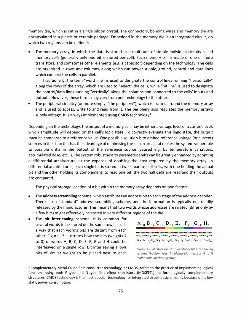
• The bit interleaving scheme. It is common for
several words to be stored on the same row, in such
a way that each word’s bits are distant from each
other. Figure 12 illustrates how the bits (weights 7
to 0) of words A, B, C, D, E, F, G and H could be
interleaved on a single row. Bit interleaving allows
bits of similar weight to be placed next to each
4 Complementary Metal-Oxide-Semiconductor technology, or CMOS, refers to the practice of implementing logical functions using both P-type and N-type field-effect transistors (MOSFETs), to form logically complementary structures. CMOS technology is the most popular technology for integrated circuit design, mainly because of its low static power consumption.
Figure 12: Illustration of an arbitrary bit interleaving scheme (bottom row) involving eight words A to H (color code on the top row).

26
other; this makes it easier to multiplex their associated bit lines into a single sense amplifier.
Interleaving also brings a higher immunity to Multiple-Bit Upsets (MBU, see next chapter); a single
particle is less likely to affect several bits of the same word if their memory cells are distant from each
other.
3) Operation To perform an operation on the memory, a
command must be sent by setting its control inputs
at specific values according to a pre-established
timing. An access is made to the memory location
designated on the component’s address bus: the
periphery sets several transmission gates5 to
electrically connect the control and data lines of the
relevant memory cells to the periphery’s. The
periphery decodes the command (typically “read”
or “write”) and accordingly readies subsystems for
the operation to come:
• for a “read” operation, the states of the
accessed memory cells are determined. For
example, in SRAMs, this is done by pre-charging
all bit lines to a certain voltage, then selecting
the row containing the relevant cells. The cells
containing e.g. a logic ‘0’ will discharge their bit
lines faster than the cells containing a logic ‘1’;
after a short period, the voltages of the bit lines
are evaluated by very sensitive analog circuits
called sense amplifiers. This evaluation gives
the information stored in the memory cells; this information is stored in an output buffer, and output
on the memory’s data bus.
• for a “write” operation, the bit lines are each set at ‘1’ or ‘0’ depending on the data to be written;
then, the word containing the relevant memory cells is selected, and the data in these cells will be
overwritten by the information stored on their bit lines.
The exact sequence of operations carried out on the control lines depends on the technology used to
manufacture the memory cells, some of which will be reviewed in the next section.
5 A transmission gate is a CMOS circuit used to electrically connect or disconnect two signal lines. The transmission gate has one control input, one data input and one data output. It is made of two transistors (one NMOS and one PMOS) connected in parallel to the two data terminals; both of their gates are connected to the control input, but one (e.g. the PMOS’ gate) is complemented by an inverter. When the control gate is at ‘1’, the PMOS can transmit high voltage levels to from the data input to the output, while the NMOS can transmit low voltage levels. If the control gate is at ‘0’, no voltage transmission can occur through either the PMOS or the NMOS, so the input and output are effectively disconnected.
Figure 13: Organization of an SRAM memory block's cells and peripheral circuitry. The same principles apply to most other memory technologies, although the number of bit lines and control lines may differ. Power supply and ground lines are omitted for clarity.

27
B. Memory cell technologies
The following subsections introduce various memory cell technologies. This section is not intended to be
an exhaustive list, but rather a quick overview of the state-of-the-art. SRAM, DRAM and flash technology
are well-established and by far dominate the market. FRAM and MRAM memories are two emerging
technologies which offer performances comparable to SRAM and DRAM cells while achieving non-
volatility.
1) Static Random-Access Memory (SRAM) First released to the market by Intel in 1969, Static Random-
Access Memories (or SRAMs) have since then been the choice
devices for high-performance applications. Typical SRAM cells
(Figure 14) are made up of six transistors; two of them are used
as access transistors, while the other four form two
interconnected inverters. The outputs of the inverters are
connected to each other’s inputs, so that their configurations
are always stable and complementary. The two possible
inverter configurations are used to represent the data stored
in the cell; this configuration disappears if power supply is
disconnected, so SRAM memory is volatile.
SRAM cells allow extremely fast read/write performance (as low as 10 ns), low power consumption
(particularly when idle), excellent endurance and easy manufacture (complete compatibility with
standard CMOS manufacturing processes). However, since they contain many transistors, SRAM cells
require a large die area; this means that they cannot reach very high densities, and makes them expensive
to manufacture. Another drawback of SRAM memories is their vulnerability to radiation (as detailed in
Chapter 4). Their typical usage is in high-performance standalone memories, or as embedded memory
within a more complex chip (e.g. processors and field-programmable gate arrays, FPGAs) where they are
used to implement registers and caches.
Two different models of SRAM were used to provide data for this study; the main results are presented in
Chapter 7.
2) Dynamic Random-Access Memory (DRAM) Dynamic Random-Access Memory (DRAM) cells are made of
one access transistor (sometimes two) and one capacitor
(Figure 15). The capacitor may or may not be charged, which is
used to represent ‘0’ or ‘1’ logic states. Leakage current
through the access transistor(s) and/or the capacitor lead to
capacitor discharge; this means that DRAM cells are volatile
and must be periodically “refreshed” (rewritten) to retain their
information (hence the “dynamic” name). Reading the cell also
discharges the capacitor, which means that the cell must be
rewritten after each read.
DRAM cells allow fast read/write performance (down to a few
tens of nanoseconds) and do not require much area for
Figure 14: Schematic of an SRAM memory cell. Figure from the public domain. WL = word line, BL = bit line.
Figure 15: Schematic of a DRAM memory cell. Figure from the public domain.

28
implementation (in particular since the advent of stacked-capacitor and trench-capacitor technology).
This makes DRAM an ideal technology in applications where large quantities of high-performance memory
are required at a reasonable cost (e.g. computers’ general-purpose working memory). One drawback of
DRAM technology is its need for complex driving circuits, due to the need to perform periodic refresh
operations. DRAM memory cells are also sensitive to radiation.
DRAM technology’s sensitivity to radiation was not surveyed in this study; the present section is included
for information only, as DRAM is a well-established technology.
3) Flash memory Flash memories consist of a structure called a floating-gate
metal-oxide-semiconductor field-effect transistor (MOSFET).
Floating-gate MOSFETs have an additional gate between the
control gate and the channel, which can be charged or
discharged by hot carrier injection and tunnelling through the
thin surrounding dielectrics. The quantity of charge stored in
the gate allows the MOSFET to reach two (or more, in the case
of multi-level cells) levels of conductivity, which is used to
determine the cell’s logic state. Figure 16 exhibits a schematic
cross-section view of a flash memory cell.
Flash memory cells are non-volatile, which means that they will remain in their logic state (and hence
preserve the data) if the power supply is discontinued. Since they only consist of one transistor, they can
achieve extremely high packing density, which makes their cost per bit very competitive. However, they
require high operating voltages, do not achieve high read/write performance, and have poor endurance
(generally thousands up to hundreds of thousands of erase cycles). These characteristics make flash
memories most suitable for long-term and/or mobile data storage applications.
The interested reader can turn to Ref [59]. for more information on flash technology. Flash memories are
sensitive to radiation, as detailed in Chapter 4, and some of the results gathered on flash memories during
this study’s irradiation campaigns are available in Chapter 7.
4) Ferroelectric Random-Access Memory (FRAM) In a similar fashion to DRAM cells, FRAM cells are made of one
access transistor and one ferroelectric capacitor (Figure 17).
In place of the traditional dielectric layer, this component
uses a ferroelectric material to separate the two capacitor
electrodes, which can be set in one of two possible electric
polarizations by applying strong external electric fields. The
built-in potential allows the ferroelectric capacitor to retain
its charge over periods ranging from at least one year to
virtually unlimited, depending on the device’s operating
temperature [60]. Reading the cell information is done by
discharging the capacitor to the bit line; this operation
effectively destroys the information. Hence, like DRAM cells,
FRAM cells must be restored (re-written) after readout. [61]
Figure 16: Cross-section schematic of a flash memory cell.
Figure 17: Schematic of an FRAM cell. Figure from the public domain.

29
FRAM memories allow fast access and read/write times (a few tens of nanoseconds), have excellent
endurance, low power consumption and are non-volatile, which means that FRAMs could take on some
of the roles traditionally taken on by fast volatile memories and slow non-volatile memories. FRAM
memory cells have the additional advantage to be immune to radiation; however, the peripheral circuitry
of FRAM devices is implemented with traditional CMOS technology, so FRAM devices as a whole are not
immune to radiation. The results of this study’s irradiation campaigns on FRAM devices are available in
Chapter 7.
5) Magnetoresistive Random-Access Memory (MRAM) MRAM cells consist of a magnetoresistive element,
called a magnetic tunnel junction (MTJ), which is
sometimes associated to an access transistor (Figure 18).
The MTJ consists in one layer of material with a fixed
magnetic polarization, and one or more layers with a
variable magnetic polarization (or “free layers”), which
can be oriented by the application of external magnetic
fields. The resistance of the MTJ is low when the layers
are polarized in the same direction, and its resistance is
high when their polarizations differ. The logic state of the
cell can be sensed by applying a certain voltage and
sensing the output current. Writing data to the cell is
done by passing carefully-timed current pulses through
the bit and word lines, with the induced magnetic fields
coercing the free layer(s) into a new polarization.
Several variations of the MRAM technology have been developed – namely, toggle MRAM, spin-torque-
transfer MRAM (STT-MRAM) and thermal-assisted switching MRAM (TAS-MRAM). The latter two are a
refinement of the toggle MRAM technology, and all three rely on MTJs. The technical differences are
beyond the scope of this thesis, but the interested reader can turn to Ref. [62] for an extensive review of
the state of the art of MRAM technology. These memories are vulnerable to strong magnetic fields and
tend to have a large active power consumption, but they have short access and read/write times (a few
tens of nanoseconds), excellent endurance, can be scaled easily (in the case of STT-MRAM) and are non-
volatile, which means that much like FRAMs, they could take on some of the roles traditionally taken on
by fast volatile memories and slow non-volatile memories.
C. Device manufacturing
The manufacturing of complex devices such as memory components, which can incorporate several billion
transistors, is an automated process taking place in ultra-clean rooms, requiring a sequence of hundreds
of separate, carefully tuned processing steps.
Figure 18: Cross-section schematic of an MRAM cell. Figure from the public domain.

30
The process starts by slowly growing a large semiconductor crystal - generally silicon, sometimes specialty
materials such as germanium or gallium arsenide. (The largest crystals can be up to 300 mm in diameter
as of 2017.) The crystal is then cut in slices a few hundreds of micrometres in thickness called wafers6.
The wafers are then subjected to several steps of chemical-mechanical polishing, oxidation, etching, ion
implantation, and photolithography to form the active regions of the future transistors within the wafer;
these steps constitute the so-called Front-End of Line processes (FEOL). The latter step, photolithography,
consists in the deposition of a layer of light-sensitive compound called a photoresist on the surface of the
wafer. The photoresist is then covered by a light-blocking mask reproducing the features to be
implemented in the wafer, and irradiated with UV light. The mask is then removed and the photoresist is
chemically developed, leaving behind a patterned layer of photoresist which can be used to selectively
expose the wafer to various treatments (e.g. ion implantation, material deposition…). The photoresist
layer can then be removed chemically or mechanically. After the completion of FEOL processes, the
transistors are formed on the wafer, but they are still isolated from each other.
The Back-End of Line processes (BEOL), which consist of additional steps of oxide deposition, chemical-
mechanical polishing, etching, photolithography and metal deposition, are used to create several layers
of interconnecting wires and vias (connections from layer to layer) which are required to connect the
transistors together. Modern devices may contain over 10 of these interconnect layers above the active
silicon. At the surface of the chip, a thick dielectric layer (sometimes referred to as a “passivation layer” is
deposited to insulate and protect the fragile active layers. Bonding pads are also created on the sides of
the chip, which will be used as connection points for input and output signals. After the end of the BEOL
processes, the wafer contains a mosaic of chips.
6 This process is true for all “bulk” technologies, where the wafer is a simple slice of a large semiconductor crystal. For other technologies, such as Silicon-on-Insulator, extra steps are needed to produce a wafer.
Figure 19: Illustration of the major steps in the fabrication of a PMOS and an NMOS transistor on a P-type wafer. Figure from the public domain.

31
Finally, the wafer is tested (the individual chips each undergo functional testing, which is done by applying
contact probes to the bonding pads and test pads) and thinned from the back (backgrinding). The
individual chips are separated from each other (generally by cutting the wafer with a diamond saw), tested
again, packaged, and tested one final time.

32
Chapter IV – Radiation effects on memory components
In Chapter 2, the basic mechanisms of radiation-matter interaction were introduced. This chapter will
focus on the effect of radiation on complex structures, made of materials with different properties and
sometimes subjected to electric fields, such as transistors and other components found inside integrated
circuits.
A. Total Ionizing Dose (TID) effects
TID effects take place when devices containing dielectrics (or “insulators”) are exposed to ionizing
radiation. Insulators are materials allowing very little electrical conduction to take place, because of their
high electrical resistance. This is a consequence of their electronic band structure: their valence band is
completely filled, their conduction band is completely empty, and the two bands are separated by a large
band gap. This means that electrical insulators have extremely low concentrations of free charge carriers
(free electrons and holes), which are necessary for electrical conduction to take place. A detailed
exposition of electronic band theory would be beyond the scope of this work – but the reader can turn to
the first chapters of Ref. [47] for further explanations.
As discussed in the previous chapters, when ionizing radiation interacts with a target material, free charge
carriers (electrons and holes) are generated. When the target material is an insulator, the resulting free
carriers have very low mobility (holes particularly so) [48]. In the absence of an applied electric field, the
free carriers will not be separated and are likely to recombine (one free electron and one hole can
annihilate each other). However, if the irradiated insulator is subjected to an electric field, the carriers can
drift; the electrons will be swept towards the higher potential while the holes will remain in place in the
material, due to their lower mobility. Over time, the bulk of an electrical insulator subjected to ionizing
radiation will accumulate positive charge, because of the trapping of holes. Additionally, the generation
and transport of holes in the oxide can have the effect of liberating otherwise static impurities forming
neutral impurity complexes (such as H+ and OH- ions introduced during oxide growth). Under the right
bias conditions, these ions can drift until they reach the Si-SiO2 interface, where they can react with Si-H
bonds (forming H2), Si-OH bonds (forming H2O) and leaving behind dangling Si bonds [63]. This results in
the presence of trapping centres at the interface, which can trap either positive of negative charge
carriers, depending on the conditions. This accumulation of charge will affect electric fields within and
surrounding the insulator. When this occurs within an integrated circuit, its operation can be affected; the
consequences of the generation and subsequent accumulation of positive charge carriers (holes) in
insulating materials within an electronic device are designated as Total Ionizing Dose (TID) effects.
Several factors impact this charge trapping mechanism, with some of the most important being the
presence and magnitude of an electric field in the insulator (component bias voltage), the insulator’s
temperature and thickness, and the presence of defects in its structure which can act as hole traps.
Discussing these factors would be beyond the scope of this work, but the interested reader can turn to
Ref. [64] for a review of the mechanisms behind TID effects.
Two typical examples of TID effects will be given in this section. One is the creation of parasitic conducting
paths along the edges of transistor channels. On Figure 20, a three-quarters schematic view of an
accumulation-type N-type Metal-Oxide-Semiconductor Field-Effect Transistor (N-MOSFET) is given. Along
the edges of the transistor are two large blocks of silicon dioxide; these are insulation trenches (commonly
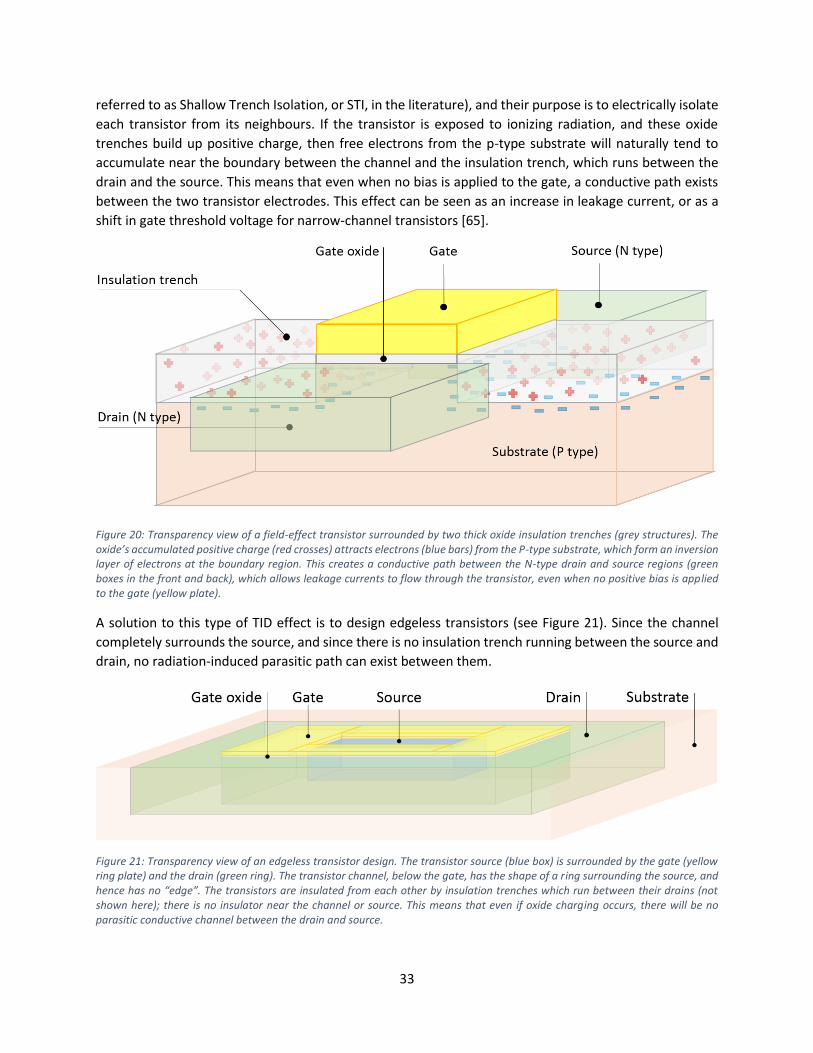
33
referred to as Shallow Trench Isolation, or STI, in the literature), and their purpose is to electrically isolate
each transistor from its neighbours. If the transistor is exposed to ionizing radiation, and these oxide
trenches build up positive charge, then free electrons from the p-type substrate will naturally tend to
accumulate near the boundary between the channel and the insulation trench, which runs between the
drain and the source. This means that even when no bias is applied to the gate, a conductive path exists
between the two transistor electrodes. This effect can be seen as an increase in leakage current, or as a
shift in gate threshold voltage for narrow-channel transistors [65].
Figure 20: Transparency view of a field-effect transistor surrounded by two thick oxide insulation trenches (grey structures). The oxide’s accumulated positive charge (red crosses) attracts electrons (blue bars) from the P-type substrate, which form an inversion layer of electrons at the boundary region. This creates a conductive path between the N-type drain and source regions (green boxes in the front and back), which allows leakage currents to flow through the transistor, even when no positive bias is applied to the gate (yellow plate).
A solution to this type of TID effect is to design edgeless transistors (see Figure 21). Since the channel
completely surrounds the source, and since there is no insulation trench running between the source and
drain, no radiation-induced parasitic path can exist between them.
Figure 21: Transparency view of an edgeless transistor design. The transistor source (blue box) is surrounded by the gate (yellow ring plate) and the drain (green ring). The transistor channel, below the gate, has the shape of a ring surrounding the source, and hence has no “edge”. The transistors are insulated from each other by insulation trenches which run between their drains (not shown here); there is no insulator near the channel or source. This means that even if oxide charging occurs, there will be no parasitic conductive channel between the drain and source.

34
The floating-gate MOSFETs at the heart of flash memory cells also suffer from TID effects. Charge-
generated holes accumulating in the insulators surrounding the floating gate can drift, be collected by the
gate and recombine with the trapped electrons, thereby neutralizing part of the stored charge.
Additionally, the accumulation of positive charge around the gate partially masks the eventual negative
charge stored in the gate. These two mechanisms lead to a drift in the floating-gate MOSFET threshold
voltage with increasing TID [66]; beyond a certain point, this drift will prevent a correct evaluation of the
cell’s logic state, causing data corruption.
B. Single-Event Effects (SEEs)
Single-Event Effects are events where the operation of an electronic component is affected by the strike
of a single energetic particle. Unlike TID effects, which appear after extended periods of radiation
exposure and require charge build-up, SEEs are prompt phenomena which take place on a timescale
generally measured in nanoseconds, and can occur in pristine devices. There are several subcategories of
SEE [67]:
• Single-Event Transients, or SETs. These can be momentary voltage excursions in the output of an
analog circuit, or a transient change in the output value or in an internal node of a logic circuit;
• Single-Event Upsets, or SEUs. These cause the disruption (upset) of the logic state of one or more
memory cells. SEEs resulting in only one upset are called Single-Bit Upsets, or SBUs, while those
resulting in several upsets are called Multiple-Cell Upsets, or MCUs. If several of the upset cells
belong to the same logic word, then the event is referred to as a Multiple-Bit Upset, or MBU.
• Single-Event Functional Interrupts, or SEFIs. During a SEFI, an electronic component loses some
or all functionality. These events are generally caused when a device’s control circuitry is affected
by radiation, which places it in an unpredicted logic state. They may be either transient or stable;
in the latter case, cycling power to the device is required to recover functionality. SEFIs may also
be permanent if an internal component is damaged.
• Single-Event Latch-up, or SEL. These events occur in bulk semiconductor7 devices, when the
current induced by the collection of charge generated by an ion strike turns on a parasitic thyristor
structure (PNPN or NPNP) under bias inside the component. SELs do not occur in Silicon-on-
Insulator (SOI) devices [68], which do not contain PNPN parasitic structures [69].
• Single-Event Burn-out, or SEB. These occur when an ion strikes a semiconductor junction under
very high reverse electrical bias (as is the case in power devices). In power diodes, the radiation-
induced charge carriers (and eventual secondary avalanche-generated carriers) locally raise the
temperature of the semiconductor; this allows a transition between a stable low-current bias
point to a stable high-current bias point on the device’s I-V curve, generating additional heating
and inducing positive feedback [70]. In power MOSFETs, the collection of radiation-induced
charge carriers may cause a voltage drop in the body potential; this may turn on a parasitic
transistor (NPN structure) between the source and drain [71]. In either case, the ensuing high
current leads to device destruction by thermal runaway (burn-out).
7 “Bulk” refers to manufacturing technologies where the component is implemented on a monocrystalline silicon substrate. This is in opposition to Silicon-on-Insulator technologies, where the substrate contains layers of insulating material (typically silicon dioxide or sapphire).

35
• Single-Event Gate Rupture, or SEGR, where a single energetic particle strike results in the
breakdown of the gate oxide. This leads to an increase in gate leakage current, and can lead to
device failure [72].
The present work deals mainly with the first four categories, with a focus on SEUs and SEFIs.
To understand the root causes behind SEUs and SEFIs, it is necessary to understand the mechanisms by
which the charge deposited in a semiconductor during an ion strike can be collected. As was discussed in
Chapter 2, charged particles passing through a semiconductor generate a “cloud” of free charge carriers
along their path. In the absence of an electric field, there will be no carrier drift; the electrons and holes
will remain close to each other and are likely to recombine, and only a minor fraction of the deposited
charge may reach a conductor via diffusion and be collected. Conversely, if an electric field is present (as
is the case across PN junctions8), the generated holes will drift towards the lowest potential, while the
free electrons will drift towards the highest potential. This charge separation prevents recombination and
leads to a high collected charge yield. As the charge carriers get collected at the semiconductor-metal
interface, a current pulse occurs at the component’s terminals – which will translate into a voltage pulse
depending on the capacitance of the connected nodes. This pulse can disrupt the circuit, and create events
such as SETs, SEUs and SEFIs. The following subsections will illustrate these possibilities.
1) Single-Event Transients (SETs) Figure 22 represents a logic circuit made up of two OR
gates and one AND gate connected in series, which
will be used to illustrate SETs and the conditions. Let
us consider a situation where input terminals A, B and
C are at a low voltage (logic ‘0’) and input D is at a high
voltage (logic ‘1’). In this situation, the output terminal
S is at ‘0’.
If one of the output transistors of OR1 is struck by an ion, a voltage pulse may appear at the output of OR1
– and so at one of the inputs of OR2. If this pulse is high and long enough, it will affect the output of OR2,
which will briefly output ‘1’. In turn, the transient at the end of OR2 will be captured by the AND gate, and
the output of the whole circuit S will briefly register ‘1’. This temporary change in the value of the circuit
caused by a single ion strike is caused a Single-Event Transient.
For an SET to produce an error, certain conditions on the ion strike position and generated pulse
characteristics must be met, notably [73]:
8 A PN junction is the boundary between a P-doped and an N-doped region of a semiconductor. This structure possesses unique electrical characteristics; in particular, under neutral or reverse bias (N side at a higher potential than the P side), the electrons close to the boundary on the N side will recombine with the holes closer to the boundary on the P side. In this case, around the PN junction, the semiconductor will be depleted of its free charge carriers, and the charge coming from the dopant atoms will produce an electric field spanning across the depletion region.
PN junctions are the elementary building blocks of many electronic components, such as PN diodes, bipolar junction transistors and field-effect transistors.
Figure 22: Schematic of logic circuit made of two OR gates and one AND gate connected in series.

36
• the pulse must be high and long enough to affect the following gate(s); otherwise it will fade out
through electrical masking. Indeed, all logic gates have a limited bandwidth, and will not respond
to small enough perturbations in their inputs.
• the following gate or memory element must be able to latch the pulse; indeed, a transient voltage
pulse occurring at the input of a synchronous (clocked) gate outside of its temporal latching
window will not be propagated at the output. This is called temporal masking.
• the ion must strike a critical node – that is, a node which, if upset, will impact the logic nodes
downwards. For example, let us consider another situation where A, B, C and D are at ‘0’; in this
case, the occurrence of an SET at the output of OR1 or OR2 will not be able to propagate until the
output node S, because the second input D of the AND gate is ‘0’. This is an example of logical
masking.
Single-Event Transients can also occur in analog circuits – for example, voltage pulses at the output of a
voltage amplifier or charge pump.
2) Single-Event Upsets (SEUs) An SEU is the corruption of the data contained in one or more memory cells following a particle strike.
Typically, SEUs occur after an ion strike located directly on the memory cell (or in its vicinity), with the
ensuing charge collection disrupting the cell’s state. They can also result from an SET occurring in the
peripheral logic during a write operation. The mechanisms at play behind SEUs differ depending on the
memory cell technology.
Figure 23 illustrates the series of events by which an SRAM cell is upset by an ion strike:
• The left-hand schematic represents the cell in its initial state: red lines are at a high potential and
blue lines at a low potential, green transistors are in on-state and black transistors are in off-state.
• The central schematic illustrates the effect of an ion strike on an off-state MOSFET: the transistor
is effectively turned on as the charge collection generates a current pulse. Its inverter is disturbed,
and its output temporarily raised to an intermediary potential between the ground and VDD. Since
this output is connected to the input of the second inverter, the second inverter may in turn be
disturbed and its output lowered to an intermediary potential, inducing a positive feedback on
the first inverter.
• The two unstable inverters may either recover their original states, or stabilise in opposite states
(right-hand schematic); in the latter case, the cell has effectively been upset and its data
corrupted.
Flash memory cells can also suffer from SEUs. As discussed in Chapter 3, flash memory cells are made of
a floating-gate MOSFET. The cell can be written to by emptying or storing electrons in the floating gate,
Figure 23:: Illustration of an SRAM cell being struck by an ion and suffering an SEU.

37
which is located between the channel and the control gate. The presence or absence of charge in the
floating gate modifies the threshold voltage of the transistor (by “screening the control gate”), and
determines whether the cell will be read as containing a ‘0’ or a ‘1’. In a flash memory array holding
random data, the threshold voltages Vth of the cell population follow a statistical distribution, such as seen
on Figure 24 (black curves).
Heavy ions striking a flash memory cell affect its threshold
voltage. The phenomenon is reviewed in [74]. The
underlying mechanisms are not yet perfectly understood,
but the most likely explanations are:
• the formation of a transient conductive path
through the gate oxide, allowing the discharge of
the floating gate [75];
• a transient carrier flux: the excitation of the
trapped carriers by the impinging particle gives
them enough energy to tunnel out of the floating
gate [76];
• positive charge trapping around the floating gate
[77].
Regardless of the mechanism (or combination of mechanisms) at play, the consequence of heavy-ion
irradiation is a modification in the threshold voltage distribution of the irradiated cell population (orange
curve in Figure 24). The threshold voltages of the cells hit by heavy ions shift towards an “intrinsic” value,
while the threshold voltages of the rest of the cells are unaffected. This gives rise to secondary peaks in
the distribution of threshold voltages; the height of these peaks is determined by the ion fluence, and
their distance to the main peaks by the ion LET and the electric field in the gate oxide [74]. Cells whose
threshold voltage come to cross the limit voltage Vread will, upon reading, be interpreted as holding the
wrong data – which constitutes an SEU.
Some memory cell technologies are inherently resilient to SEUs, because they rely on other physical
mechanisms than charge storage to store information. For instance, FRAM memory cells have
demonstrated invulnerability to direct upset by heavy ions up to xenon between 0° and 60° (effective
LETs9 of 64 MeV.cm2.mg-1 and 128 MeV.cm2.mg-1 respectively) at fluences of 1.5*107 cm-2 and 1.0*106 cm-
2 respectively [78]. MRAMs also exhibit heavy-ion SEU invulnerability up to xenon at 60° (effective LET 112
MeV.cm2.mg-1) at a fluence of 1.0*107 cm-2 [79]. The main radiation hardness concern for these memory
cell technologies is the formation of crystalline defects via displacement damage. However, since the
CMOS peripheral circuits used to drive the memory cells are typically much more sensitive to radiation,
the sensitivity of the memory cells is not a limiting factor. In Chapter 7, the results of radiation test
9 The “effective LET” is a metric used to compare the effects of irradiation with particle beams striking the target at different incidence angles. The effective LET is equal to the normal ion LET divided by the cosine of the angle of incidence (this means that the effective LET is always superior or equal to the normal LET). This model allows for a simplified comparison of results obtained with different beams, but shows its limits when the dimensions of the charge collection volume are small.
Figure 24: Distribution of the threshold voltages of the memory cells in a flash array after arbitrary data writing (black curves), and after subsequent heavy-ion irradiation (orange curves).

38
campaigns carried out on FRAMs for the needs of this study show that the CMOS periphery is the sole
contributor to the devices’ failures.
3) Single-Event Functional Interrupts (SEFIs) When ion strikes produce SETs or SEUs in critical locations of a memory’s periphery, these circuits may
accidentally enter a state where they cannot perform their designed function. This causes a category of
events known as Single-Event Functional Interrupts, or SEFIs. By nature, SEFI scenarios can broadly differ
from one device model to another, since SEFIs are heavily dependent on the design of the device’s
peripheral circuitry.
To illustrate SEFIs, let us consider the following,
simplified memory array block in Figure 25. Even
though the block is only meant to contain four 8-
bit words, it is common practice to implement
the block with redundant columns (and lines, not
shown here). This is done to improve
manufacturing yield: when a defective column is
detected during factory testing, the
manufacturer can reassign the faulty column to a
spare, thereby “saving” the memory block.
Without this redundancy mechanism, defective
elements (which are a very common occurrence
in complex integrated circuits) would
compromise device operation, and the compromised devices would need to be discarded.
The column reallocation operation can be done during factory testing via several methods, such as using
sets of electrically-set or laser-set fuses and antifuses to connect and disconnect signal lines. Some
devices, however, are reorganized programmatically; this is done by rewriting internal non-volatile
memory (distinct from the general-purpose memory array) dedicated to redundancy information storage.
When the device is powered up, this information is fetched from the non-volatile redundancy memory
and loaded into redundancy registers10, which in turn drive transmission gates and other circuits, leading
to the desired array reorganization.
If an SEU occurs in a redundancy register controlling spare column reallocation for our considered memory
block, the spare will be used to replace the original column, so that the data contained in the spare will
be fetched during subsequent memory accesses. However, since the spare contains arbitrary data, which
likely does not match the data of the original column, subsequent accesses to this memory block will
return erroneous data as long as the SEU in the hardware register is not corrected.
This is only one example of numerous possible SEFI scenarios. Further examples of SEFIs, identified in test
data gathered throughout the course of this work, will be presented in Chapter 7.
10 Hardware registers are circuits which are closely related to memory cells. They can store data, and they are typically implemented using latches – bistable circuits whose operation principle is similar to that of SRAM cells. However, they also have special hardware-related functions beyond those of ordinary memory. The information stored in register cells – their logical state – can be used to directly impact the configuration of other logical circuits in the device.
Figure 25: Schematic representation of a memory block containing four 8-bit words and one spare column.

39
4) Single-Event Latch-ups (SELs) Single-Event Latch-ups, or SELs, occur when the passage of a charge particle and subsequent charge carrier
collection triggers a parasitic PNPN structure (thyristor) within the component, thereby creating a self-
sustaining conducting path between two conductors at different potentials. A high current may flow
through the semiconductor, which can have detrimental consequences on the component’s performance:
higher power consumption, high IR drops11 in internal lines, stuck signals, and possibly device destruction
via thermal runaway.
Figure 26 illustrates a typical configuration of N-
type and P-type regions inside a CMOS circuit (in
this case, implemented in a P-type substrate).
Two parasitic bipolar junction transistors (BJTs)
can be identified: an NPN between the NFET’s
source (as an emitter) and the N-well, with the
P-type substrate as a base; and a PNP between
the PFET’s source (as an emitter) and the P-type
substrate, with the N-well as a base. The base of
the parasitic NPN is connected to the GND tap12,
but the silicon substrate and semiconductor-
metal junction have a relatively high resistance;
the same can be said of the PNP’s base, loosely
connected to the VDD well tap through the N-
well.
If an ion strikes through the N-well, the generated charge carriers will be separated by the electric field;
the holes will recombine with the majority carriers in the N-well, while the electrons will drift towards the
N+ well tap at VDD. If enough electrons are collected, their motion through the low-doping, resistive N-
well will create a temporary voltage drop in the well. If this voltage drop is sufficiently high, the P+ source
of the PFET will start to emit holes through the N-well and into the P substrate, thereby turning on the
parasitic PNP. The injected holes will travel through the substrate to the P+ electrode contact at GND. If
enough holes are injected, their motion through the low-doped silicon will induce such a rise in substrate
voltage that the N+ source of the NFET will start to emit electrons through the P-type substrate and into
the N-well. These electrons will be collected by the N+ electrode at VDD; at this point, each BJT is injecting
minority carriers into the other BJT’s base, creating a positive feedback loop which allows a sustained flow
of current from the VDD to the GND supply rails. The current flows through the bulk of the silicon and
bypasses the gates of the MOSFETs entirely, which means that the latch-up current cannot be influenced
via the MOSFET gates; the only way to recover from this situation is to lower the potential of the VDD
supply rail (or switch power off entirely) until the parasitic BJTs turn off.
It is sometimes possible to design components in a way which minimizes the risks of SEL onset. SOI
components, for example, are immune to SELs, because their architecture does not contain the PNPN
11 IR drops are voltage drops in a signal or power line caused by the resistance of the line itself. 12 Well taps, also called well ties, are used to set (or “tie”) the potential of a semiconductor to a reference potential. In Fig. 7, the leftmost P+ contact is a well tap setting the substrate at the GND potential, and the rightmost N+ electrode is a well tap tying the N-well to VDD.
Figure 26: cross-section schematic view of a P-type substrate containing an N-type MOSFET, and a P-type MOSFET in an N-well (a typical structure in CMOS circuits). The parasitic thyristor's NPNP structure is indicated by the orange circuit diagram.

40
structures necessary to SEL onset; each transistor is isolated from its neighbours by the buried oxide and
the field oxide [69]. It is also possible to harden bulk devices against SELs by using lower bias voltages,
higher substrate doping concentrations (to lower substrate resistivity), additional well taps (to lower the
substrate-reference junction resistivity) and careful geometry (to minimize the gain of the parasitic BJTs).
SELs are more likely to occur at high temperatures and at high impinging ion LETs.
SELs are serious failures, because of the potential for component damage via thermal runaway. It is
possible to mitigate the effects of SELs by protecting components with delatcher circuits; these act as
switches placed in series with the power source of the component to be protected, turning off when the
supply current exceeds a threshold value. This solution has its limits, though, as SELs can produce parasitic
current flows of various intensities, which may not necessarily produce an appreciable change in the
component’s main current consumption. What’s more, some devices (e.g. memories, processors, FPGAs)
have naturally varying power consumption profiles (depending on their activity), so finding an appropriate
current consumption threshold is not always possible.
41
Chapter V – Radiation testing of memory components
When trying to assess the radiation sensitivity of a component, it is common practice to obtain
experimental data via radiation testing. This chapter will introduce the standard procedures and
methodologies for Radiation Hardness Assurance (RHA) testing in general, and for radiation testing of
memory components in particular.
A. Radiation Hardness Assurance
As discussed in the previous chapters, radiation can have detrimental effects on electronic components.
The build-up of ionizing dose can lead to TID effects; displacement damage can degrade material
properties and component performance; finally, individual particle strikes can trigger non-destructive
(SET, SEU, SEFI) and destructive failure events (SEFI, SEL, SEB, SEGR). The high level of system reliability
required in some applications (typically space, aeronautics and automotive engineering) makes Radiation
Hardness Assurance (RHA) a key process in achieving mission success. RHA typically involves the following
steps:
• At the mission proposal/feasibility phase: definition of the radiation specifications
o Preliminary radiation environment specification (particle spectra and flux, peak and average)
o RHA specification (at system level): mission duration, technical performance goals, availability,
required design margins, test requirements…
• At the Preliminary Design Review (PDR):
o Final radiation environment definition
o Preliminary shielding analysis using preliminary spacecraft layout
o Final RHA specification (at equipment level). This will allow adequate parts selection.
• At the Critical Design Review (CDR):
o Evaluation of radiation data of the parts selected after PDR. (Engineers tend to favour parts with
existing radiation data and a favourable operational history. When no such parts are available, or
when existing parts do not meet requirements, then new parts must be identified, procured and
tested.)
o Final shielding analysis
o Circuit design analysis: failure rates computed from radiation testing data and predicted shielded
radiation environment
• After CDR:
o Radiation Lot Acceptance tests. Since devices can differ from lot to lot without notice, it is
important to ensure that the most critical parts used on the mission hardware behave as expected
under radiation. To this effect, other devices from the same production lot are tested.
• After Launch:
o Failure analysis. This generates feedback on the RHA process, allowing eventual mistakes to be
avoided in the future, and consolidating the operational history of the selected parts.
N.B.: This process is not rigid by nature; during a project’s development, several iterations of a design may
be submitted for radiation hardness evaluation, fall short of specifications, be revised and submitted
again. Part selection is not the only means of ensuring equipment reliability: specific circuit-level design
techniques may be used to make up for component-level shortcomings - for example, the use of Triple

42
Modular Redundancy (TMR) and Error-Correcting Codes (ECC). The equipment may also be positioned in
another, less exposed region of the spacecraft.
The RHA process depends on the radiation data available to system designers. This data measures a
component’s resilience to disturbance by radiation: for example, its parametric shifts as a function of
accumulated dose, or its failure rate in a given environment. This data comes partly from the feedback of
previous missions, but the main means of acquiring radiation data on a component is via radiation testing.
The data’s accuracy and associated uncertainty are crucial for the reliability of the final system; hence
radiation testing has been standardized by the main actors in the industry.
B. Testing standards and methodologies
To accurately predict a component’s degradation during its mission, it is necessary that the irradiation
represents the mission’s radiative environment. As discussed in Chapter 1, space radiation environments
may include very high energy particles (above one GeV per nucleon). What’s more, the particle fluence
accumulated by a spacecraft during its mission (which can last over two decades) can reach extremely
high values. Recreating these conditions in a reasonable amount of time requires facilities capable of
generating high-intensity, high-energy radiation: this is why SEE tests are typically carried out at particle
accelerators, while TID tests are done using cobalt-60 irradiators. These facilities have high operating costs
and limited beam time availability; this explains why component test campaigns are expensive, and
sometimes lengthy operations.
All major space agencies (ESA, NASA, JAXA…) have created series of testing standards for Electrical,
Electronic and Electro-mechanical (EEE) components to assist system designers and facilitate RHA
processes. Among the main series of standards are those published by the European Space Components
Coordination (ESCC) [80] and the Joint Electron Device Engineering Council (JEDEC) [81]. These standards
help ensure that the generated radiation data meets high enough levels of confidence and repeatability
for critical applications. For example, the ESCC Basic Specification No. 25100 [82], entitled “Single-Event
Effects Test Method and Guidelines”, gives directions for SEU testing, notably on the following points:
• Particle beam characteristics: energy (for protons) or LET in silicon (for heavy ions), flux, energy and
dosimetry error…
• Condition of the device under test (DUT): closed or delidded, in air or in vacuum, temperature
monitoring, number of samples to be tested, standards for traceability…
• Electrical parameters for testing: bias voltages, operating frequencies, data patterns…
• Test plan requirements: total fluence to be deposited, minimum number of energy/LET steps to be
carried out, recommendations regarding TID effects during SEE testing…
Radiation test data generated according to the specifications of this ESCC standard may be submitted to
the ESCC for inclusion in an online radiation data repository, the ESA Radiation Reports [83]. An equivalent
US repository is the NASA Goddard Space Flight Center’s Radiation Database [84]. These structures have
been created to facilitate data exchange, speed up RHA processes, and avoid redundant radiation testing.
Typically, memory components undergo a TID test, a proton SEE test and a heavy-ion SEE test. The reason
for carrying out separate proton tests is that protons represent the largest share of the ion fluence
received by a spacecraft. However, heavier ions can have much higher LETs and are more likely to trigger
failures, hence the need for heavy-ion SEE testing. Obtaining separate heavy-ion and proton response

43
data for a component also allows failure rate predictions in environments with different proton and
heavy-ion spectra (e.g. GEO and LEO orbits).
C. Concepts and metrics for radiation testing
To effectively assess a component’s response to radiation, it is important to have appropriate metrics and
to measure the relevant variables. These depend on the component type; the ECSS Basic Specifications
(e.g. [82] for SEE and [85] for TID) and ECSS Detail Specifications (e.g. [86] for certain types of
asynchronous SRAMs) provide guidelines as to which parameters are relevant for monitoring during a test
campaign.
During SEE testing of memory components, three types of failure events may occur: SEU, SEFI and SEL. An
SEE radiation testing campaign shall determine:
• The device’s SEU cross-section (as a function of LET for heavy ions, and as a function of particle energy
for protons). This represents the sum of all sensitive areas on the die surface which if hit by an
impinging ion, and if enough energy is deposited, will produce an SEU. Its formula is: 𝜎𝑆𝐸𝑈 =#𝑒𝑟𝑟𝑜𝑟𝑠
𝑓𝑙𝑢𝑒𝑛𝑐𝑒
The SEU cross-section is typically zero at low particle energy/LET, then increases sharply past a
certain energy/LET threshold, and eventually tends towards an asymptotic maximum value at high
energy/LET. Two important values reflect this behaviour:
o The SEU threshold LET/energy, below which the device is effectively insensitive to SEU.
o The saturation SEU cross-section, which is the asymptotic value towards which the SEU curve
tends at high LET/energy.
It is common to create a Weibull fit of the SEU cross-section curve; this Weibull curve is simply defined
by the threshold SEU/energy, the saturation cross-section, a scale and a shape parameters, which
makes it a convenient input for further standardized single-event rate calculations.
It is also interesting to consider the device’s SEU cross-section per bit; this metric allows a
comparison of the radiation sensitivity of memory components of different capacity. Its formula is:
𝜎𝑆𝐸𝑈𝑏𝑖𝑡=
#𝑒𝑟𝑟𝑜𝑟𝑠
𝑓𝑙𝑢𝑒𝑛𝑐𝑒 × #𝑏𝑖𝑡𝑠
• The device’s LET threshold for SEL occurrence (if possible, as a function of supply voltage; otherwise,
at the nominal operating voltage).
o The minimum bias voltage for SEL occurrence (if different bias voltages can be tested)
• The device’s SEFI cross-section (as a function of particle LET/energy).
TID testing campaigns, on the other hand, shall determine the drift of the component’s electrical
parameters (e.g. main supply current, input/output pin current, memory access delays…) and eventual
failures as a function of accumulated dose. The parameters to be monitored depend on the component
type, and are defined in a series of ECSS Detailed Specifications.

44
D. Algorithms for memory testing
To adequately detect faults occurring in a memory device, the choice of testing algorithm is important. A
variety of memory test algorithms have been developed, which are routinely used by manufacturers to
check the functionality of their devices. Among these test algorithms, “March tests” are the most
commonly used at production level because of their high effectiveness and their low complexity (linear
with the size of the memory). March tests consist in one or more “elements” (sequences of read and write
operations) to be applied to every memory address in a given order. Manufacturing defects can induce
several types of faults in memories, including (not exclusively) [87]:
• Stuck-at fault (SAF), where the state of a memory cell is stuck to either ‘0’ or ‘1’, and cannot be
changed;
• Transition fault (TF), where a memory cell is incapable of switching from one state to the other;
• Coupling fault (CF), where the state of a cell (victim) is influenced by the state or operations
carried out on another cell (aggressor);
• Neighbourhood pattern sensitive fault (NPSF), where the state of a cell is determined by the state
of a set of neighbouring cells;
• Address decoder faults (AF), where either:
o with a certain address, no cell will be accessed;
o a certain cell will not be accessible;
o with a certain address, multiple cells are accessed simultaneously;
o a certain cell can be accessed with multiple addresses.
and various combinations of these basic faults.
Without going in too much detail – the interested reader can turn to [87] and [88], which are
comprehensive reviews of chip testing techniques – each of these types of basic faults requires a specific
sequence of operations to be sensitized and observed. This implies that algorithms may be incapable of
detecting all types of faults; for example, the March C algorithm [89] can detect SAFs, TFs, and unlinked
CFs (CFs which involve cells not involved in other faults), while the MATS+ algorithm [90] can only detect
SAFs. Testing algorithms also differ in the time (i.e. the number of operations) they require to be
completed. A shorter testing algorithm will allow faster testing, which represents a gain in productivity
for manufacturers.
March algorithms can effectively be applied to the detection of radiation-induced upsets. Since the DUTs
used in irradiation campaigns have successfully passed factory checks, and are a priori entirely functional,
the algorithms used in radiation testing campaigns focus on other specifications:
• Minimization of error masking. The point of a radiation testing campaign is to detect radiation-
induced upsets. Memory cells are typically upset between the last operation performed during
element N and the first operation performed during element N+1, because in this relatively long
interval, the algorithm is performed on the rest of the array, leaving the cell idle. SEUs are only
observed when the affected cells are accessed and read; this means that most SEUs are detected
by the first read operation of an element. This also means that algorithms with elements starting
with a write operation will, at some point, destroy information related to upset cells by
overwriting all the cells without reading them first. Hence, using an algorithm with little or no

45
masking effect (i.e. few or zero elements starting with a write operation) will ensure an efficient
data collection.
• Stimulation of the peripheral circuitry. Different testing algorithms will put different levels of
stress on different parts of the periphery. For example, it is possible to use algorithms with very
short elements (down to a single operation) and scanning the memory array in an order that
maximizes switching activity in the address decoders; conversely, it is also possible to minimize
the switching activity. Such algorithms have been used in this study, and are described in
Chapter 6.
• Maximal sensitization of the memory cells. Certain algorithms can create conditions that
maximize the sensitivity of the memory cells. An example is the Dynamic Stress Test developed in
[91], which relies on two key effects:
o When an SRAM cell is read, it is selected by pulling its word line up (see Chapter 4, Figure
14); this has the effect of discharging the bit line connected to the low node of the cell
(the inverter with the NMOS transistor ON). The current passing through the open NMOS
raises the potential of the low node, making the cell less stable during the duration of the
read operation – and more vulnerable to SEU. In the meanwhile, all the other SRAM cells
on the row are also selected by the word line, and discharge the bit lines connected to
their low nodes (all bit lines are generally left at a high voltage as long as their block is
accessed, to speed up operation). All the cells on the same row suffer the same
destabilization as the accessed cell, an effect known as Read Equivalent Stress (RES) [92].
o Carrying out several successive read operations on an SRAM cell (“read hammering”)
improves the chances of detecting resistive-open defects [92].
By performing successive read operations on each memory cell, the Dynamic Stress Test combines
these two effects to increase the sensitivity of all the memory cells in a given row of a memory
block at any given time. This can result in a non-negligible increase in the overall cross-section of
SRAM devices [93].

46
Chapter VI – Experimental setup
This chapter will present the test benches used to gather radiation data, and the software tools created
for data processing.
A. Test setups
1) Selected devices
• Cypress CY62177EV30 MoBL, a 90-nm technology, 32-Mibit13 SRAM in a 48-pin TSOP type I package.
This device has the particularity of embedding two 16-Mibit memory dies stacked vertically within a
single package.
Each die is divided into 2 planes, each plane has 64 blocks, each block has 2048 rows, and each row
contains 8 words of 8 bits. The 64 bits of each row are positioned according to an 8-bit interleaving
scheme.
• Cypress CY62167GE MoBL, a 65-nm technology, 16-Mibit SRAM in a 48-pin TSOP type I package. This
device embeds an Error-Correcting Code (ECC) functionality, which enables the correction of single-
bit errors, and can be activated or inhibited at device startup using a specific sequence of inputs. The
device is pin-to-pin compatible with the SRAM90.
The memory array is divided into 2 halves, each divided into 2 quads, each divided into 2 octants; each
of the eight octants is divided into 8 blocks. Each block holds 32768 words of 8 bits.
13 One mebibit (symbol: Mibit) is a binary multiple of the bit. 1 Mibit = 220 bit = 210
*210 bits = 1,048,576 bits.
Figure 27: Top views of one closed and one delidded Cypress CY62177EV30 devices, and side X-ray view of the device. The side X-ray view zoom-in highlights the stacked-dies architecture, with bonding wires appearing on two levels.
Figure 28: Top views of one closed and one delidded Cypress CY62167GE devices.

47
• Cypress FM22L16, a 130-nm technology, 4-Mibit FRAM in a 44-pin TSOP type II package. This part was
originally manufactured by Ramtron International, and is now manufactured by Cypress
Semiconductor after it acquired Ramtron in 2012. Devices from both manufacturers were used during
this study. This component has the largest memory capacity available on the FRAM market.
The memory array is divided into 8 blocks, each divided into 8192 pages; each of these holds 4 words
of 16 bits. The device has a special page-wise operation mode which allows faster access times.
• Everspin MR4A08B, a 16-Mibit toggle MRAM in a 44-pin TSOP type II package. This is the largest toggle
MRAM capacity available from Everspin, which is currently the only manufacturer of standalone
MRAM devices. The MRAM is pin-to-pin compatible with the FRAM. Each word contains 8 bits.
• Micron 29F32G08ABAAA, a 32-Gibit flash memory in a TSOP type I package. The device is not pin-to-
pin compatible with the SRAM65 and SRAM90.
The memory array is divided into 2 planes, each divided in 2048 blocks, each divided into 128 pages
of 8192 columns. Each column holds one 8-bit word.
Figure 29: Top views of one closed and one delidded Ramtron/Cypress FM22L16 devices.
Figure 30: Top views of one closed and one delidded Everspin MR4A08B devices.
Figure 31: Top views of one closed and one delidded Micron 29F32G08ABAAA devices.

48
For convenience, future references to these devices will be made as SRAM90, SRAM65, FRAM, MRAM
and flash respectively.
These devices are all COTS. They were procured in several steps, either directly from the manufacturer or
from retailers. The delidding operations, when not carried out by the manufacturer (SRAM65), were done
in several batches by SERMA Technologies (SRAM90, FRAM, MRAM, flash) and ESA-ESTEC (flash).
2) Standalone memory test bench The several standalone memory test benches which
were used to gather experimental data during this
study are successive iterations of a design developed
at LIRMM. At the core of the design is a Digilent
Spartan-3 Starter Board Rev. E (which will be
referred to as DSSB; see Figure 32), which embeds a
Xilinx Spartan-3 XC3S200 FPGA. The DSSB has three
2*20 pin expansion connectors, which can be used
to connect expansion boards, either directly or
indirectly using ribbon cables.
Several expansion boards were designed to interface the standalone memory devices with the DSSB.
These expansion boards include Zero Insertion Force (ZIF) open-top sockets mounted on a mezzanine
board. The SRAM90 and SRAM65 devices, sharing the same package and being pin-to-pin compatible
(including power pins), were interfaced via the same expansion board; another board was used for the
MRAM and FRAM, similarly compatible. A set of jumpers on the expansion boards was used to connect
and disconnect signal lines when necessary. The flash memory was tested using a separate board, because
of its different pin layout. The use of open-top ZIF sockets and mezzanine boards allowed a direct
exposition of the delidded DUTs to the ion beams, while facilitating the replacement of DUTs during
testing campaigns and disassembly of the test bench for easy transportation. Figure 33 illustrates these
three types of expansion boards.
Figure 32: Top view of the Digilent Spartan-3 Starter Board (DSSB).
Figure 33: Expansion boards and ZIF sockets for SRAM90 and SRAM65 (left), MRAM and FRAM (centre), and flash devices (right). The top left pair of pin headers are used to connect power for the DUT; the 4-in-line pin headers on the left can be used to connect an optional delatcher mezzanine board; all other jumpers are used to connect and disconnect signal lines.

49
The expansion boards are equipped with a set of four pin headers, which can be used to insert an optional
mezzanine delatcher14 board in series with the DUT’s power supply (Figure 34). This component senses
the voltage drop created by the DUT’s supply current passing through a weak resistor, and disconnects
the DUT (via an NPN transitor) if the voltage drop exceeds 50 mV for over 10 μs. In such an event, a pulse
signal is sent to the DSSB via the expansion board for notification. By choosing the value of the sensing
resistor, the user can adapt the delatcher to accommodate different DUT supply current levels. The
delatcher restores power to the DUT after 200 ms.
The FPGA was configured with a testing program which was developed in-house, and was continually
upgraded over the years. It provides many options for functional testing:
• Static testing – the whole memory array is written with either “all
0”, “all 1”, “logical checkerboard” or “data=address” patterns.
The “data=address” pattern writes the lower 8 bits of its address
vector in every word. The DUT can be read back after irradiation
and the data compared with the template to check for SEE-
induced errors. Periodic readback operations can be programmed
with an adjustable timer; static testing can also be controlled
manually with “write X” and “read X” commands.
• Dynamic testing – all memory addresses in the array, one by one,
undergo a series of read and/or write operations (called an
element). Once all addresses have been visited, the cycle repeats
with a new element, until the user puts a halt to the test. All the
while, the DUT undergoes irradiation. Different dynamic stressing
algorithms can be used, as described below15:
o Dynamic stress [93], [94]: {↑(r1,w0,r0,r0,r0,r0,r0);
↑(r0,w1,r1,r1,r1,r1,r1);
↑(r1,w0,r0,r0,r0,r0,r0);
↓(r0,w1,r1,r1,r1,r1,r1);
↓(r1,w0,r0,r0,r0,r0,r0);
↑(r0,w1,r1,r1,r1,r1,r1)}
o March C- [95]: {↑(w0);↑(r0,w1);↑(r1,w0);
↓(r0,w1);↓(r1,w0);↑(r0)}
o MATS + [90]: {↑(w0);↑(r0,w1);↓(r1,w0)}
o mMATS+: {↑(r0,w1);↑(r1,w0)}
o Dynamic Classic [93]: {↑(w0);↑(r0);↑(w1);↑(r1)}
14 Delatchers are circuits used to protect devices in the event of a latch-up occurrence. They are typically connected in series with the device’s power supply, and disconnect them if their supply current exceeds a certain value for a certain period. 15 Operations are separated by commas, while elements are in parenthesis and separated by semicolons. The arrows
in the algorithm descriptions above indicate the direction of address scanning; if the arrow is up, the element will
be applied to all addresses from the first to the last, and vice versa.
Figure 34: Mezzanine delatcher board. The jumper is used to select one of two different sense resistors.

50
For all dynamic tests, the order in which memory locations were visited during a cycle could be
determined in a number of possible ways:
o Natural: the address vector is simply incremented or decremented at each step, so that any
addresses N and N±1 are visited consecutively
o Fast row: the address vector is changed so as to scan the memory array row after row*
o Fast column: the address vector is changed so as to scan the memory array column after column*
o LFSR: the address vector is controlled by a linear-feedback shift register (LFSR) configured so that
every address is visited exactly once per cycle, in pseudo-random fashion
o Gray: the address vector is incremented/decremented as a Gray binary vector (instead of being
treated as a natural binary vector). This ensures that only one address bit toggles between two
consecutive steps, reducing the activity of the DUT’s address decoders
o Anti-Gray: the address vector is incremented/decremented as a Gray binary vector (instead of
being treated as a natural binary vector), and is complemented every other step. This ensures that
all but one address bit toggle between two consecutive steps, maximizing the activity of the DUT’s
address decoders
*N.B.: Using the fast row or fast column addressing schemes requires a knowledge of the DUT’s
address scrambling scheme. This was only available for the SRAM90 and SRAM65 devices.
• Latch-up testing – when a delatcher board is connected to the expansion board, the test bench is
capable of detecting high DUT power current consumption. Latch-up conditions drawing sufficient
current to cause the device to exceed its specifications can be detected using this functionality.
The test bench, comprising the DSSB, expansion board, eventual delatcher, and the DUT, was connected
to a computer using the DSSB’s RS-232 serial link. A desktop power supply was used to bias the DSSB at
5V and the DUTs at 3.3V.
3) Test bench monitoring and control Both types of memory test benches were linked via an UART to a remote computer. An amateur terminal
program, ComTools [96], was used for setup control and data logging. The benches were controlled using
2-byte commands, and sent data and status updates back to the control computer using 6 or 7-byte
messages. Messages were sent back to acknowledge command reception, task completion, signal latch-
up conditions, and erroneous outputs from the DUT. When reporting errors, a message would contain the
error’s address, its data, and (for dynamic tests only) mention at which step of the stress algorithm
(operation and element) the error was detected.
The typical test run would unfold as follows:
• At first, commands would be used to manually put the test bench in the proper state (write a certain
data pattern, or start the desired dynamic stress algorithm).
• The beam would then be started manually; the team conducting the experiment monitors the
messages sent from the test bench appearing in real time on the control terminal, as well as the
current delivered to the DUT by the power supply. Depending on the situation:
o If the test run unfolds as planned, the beam would be shut down manually or automatically after
reaching a predefined deposited fluence goal.

51
o If the DUT or test setup enters a critical failure condition (permanent SEFI, severe latch-up,
monitoring software crash, etc…), the test would be aborted.
• The test data would be summarily analysed on the spot to determine the DUT response: number of
errors, presence or absence of large SEFI, etc… This preliminary information could be used to alter the
campaign’s test plan if necessary (e.g. adding additional measurement points).
• Later on, extensive data post-processing would be carried out to extract all possible information.
Figure 35 exhibits a sample from a test log obtained during heavy-ion irradiation of an SRAM65.
B. Data processing
An experimented operator can identify many distinctive features in the error messages appearing on the
monitoring console (based on the timing of their arrival, the similarity of their address and data vectors,
and the metadata), which can be very useful to monitor the DUT response in real-time during a test run.
However, automated tools are necessary to process the vast amount of data generated during a test
campaign and to perform complex operations. Two software tools have been developed for this purpose,
one in C/C++, the other in Scilab [97].
1) C processing A C/C++ software, the Test log Interpreter and Generator of Extensive Reports (TIGER), was developed in-
house to process the test data.
The test logs are read and parsed, and every
message is used to generate a pointer to a structure
(*SEU) whose fields contain the error address, data
and metadata of the message. The “SEU” structs
are then manipulated by a series of sorting and
clustering functions (the clustering functions will be
discussed further in the next section). A list of
“cluster” structures are created; each cluster
contains a chain of *SEU pointers (representing the
errors constituting the cluster), the coordinates of
its outer boundaries (xmin, xmax, ymin, ymax, tmin and
tmax), and a pointer to the next cluster.
2014/11/07 19:39:00 64 03 41 0D 08 11 64 04 70 8D 10 11 64 04 7B 69 40 11 64 07 3B E9 40 11
2014/11/07 19:39:00 64 08 05 71 20 11
2014/11/07 19:39:00 64 0C BE 46 10 11
2014/11/07 19:39:00 64 16 54 29 20 11 64 16 9F A9 01 11
2014/11/07 19:39:00 64 1C D6 4B 40 11 64 1F 96 CB 40 11
2014/11/07 19:39:01 64 12 14 DF BF 19
2014/11/07 19:39:01 64 0C 06 30 BF 19 64 0A 0D 31 DF 19 64 08 0D B1 DF 19
2014/11/07 19:39:01 64 07 72 D5 BF 19 64 05 CC 8E FE 19 64 05 CC 0E FE 19 64 04 BD 06 FB 19
2014/11/07 19:39:01 64 02 23 EF BF 19 64 02 23 6F BF 19
2014/11/07 19:39:02 64 05 19 98 02 11
2014/11/07 19:39:02 64 0F 65 15 40 11 64 10 A8 EC 02 11
2014/11/07 19:39:02 64 13 D9 98 10 11
Figure 35: Excerpt from an SRAM65 heavy-ion test log. The test bench sends 6-byte error messages starting with a header byte (“64” for error notifications), followed by three address bytes, one data byte and one metadata byte. The monitoring terminal groups the messages arriving within 100 ms of each other on a single line, and inserts a timestamp at the beginning of each line.
Figure 36: Screenshot of the TIGER tool processing a batch of SRAM90 test logs

52
Once the errors have been clusterized, TIGER can output text files containing the formatted list of clusters
and their list of errors. It can also generate bitmaps, which are a graphical representation of the data
contained in the memory array. On a bitmap, every pixel represents a bit; the pixels can be coloured to
indicate whether a bit has suffered an upset or not. Depending on the information available on the device,
it is possible to generate several types of bitmaps:
• Logical bitmaps, where the words are placed one next to another, line by line, according to their logic
address. All the bits of each word are placed consecutively to each other, always in the same order.
• Chronological bitmaps, where the words are
placed according to the order in which they
were accessed during the test. For all static
tests, and for dynamic tests carried out with
natural addressing, the chronological bitmap is
equivalent to the logical bitmap. For dynamic
tests carried out with non-natural addressing
schemes, however, the chronological bitmap
can be substantially different. Table 1
illustrates the order in which words would be
accessed using four different addressing
schemes.
Chronological bitmaps generated from dynamic
tests using the non-natural addressing schemes would be mapped as follows:
Figure 38: Chronological Gray bitmap.
Figure 39: Chronological anti-Gray bitmap.
Natural Gray Anti-Gray LFSR
0000 (0) 0000 (0) 0000 (0) 0000 (0)
0001 (1) 0001 (1) 1110 (14) 0001 (1)
0010 (2) 0011 (3) 0011 (3) 0011 (3)
0011 (3) 0010 (2) 1101 (13) 0111 (7)
0100 (4) 0110 (6) 0110 (6) 1110 (14)
0101 (5) 0111 (7) 1000 (8) 1101 (13)
0110 (6) 0101 (5) 0101 (5) 1011 (11)
0111 (7) 0100 (4) 1011 (11) 0110 (6)
1000 (8) 1100 (12) 1100 (12) 1100 (12)
1001 (9) 1101 (13) 0010 (2) 1001 (9)
1010 (10) 1111 (15) 1111 (15) 0010 (2)
1011 (11) 1110 (14) 0001 (1) 0101 (5)
1100 (12) 1010 (10) 1010 (10) 1010 (19)
1101 (13) 1011 (11) 0100 (4) 0100 (4)
1110 (14) 1001 (9) 1001 (9) 1000 (8)
1111 (15) 1000 (8) 0111 (7) 0000 (0)
Table 1: Order of visit of a 16-word address space using four different addressing schemes. Note that the XOR-based LFSR addressing used to generate the LFSR sequence cannot visit an address with all bits at '1', which would otherwise result in a deadlock.
Figure 37: Illustration of the bit/pixel placement on a logical bitmap. The subscript digits indicate the bit weight within the word; words are identified by their logic address (indicated by the normal-case numbers). The words are laid out contiguously, by increasing address, left to right, line by line.

53
Figure 40: Chronological LFSR bitmap. Since the address “1111” cannot be visited, one word will be coloured by default.
• Physical bitmaps, where every pixel is positioned according to its corresponding bit’s actual physical
storage position of in the memory array. Producing such a bitmap requires precise information on the
organization of the memory array – its address scrambling and bit interleaving schemes. On a physical
bitmap, data could be positioned according to the following, arbitrary pattern:
Figure 41: Physical bitmap generated using 4-bit interleaving and an arbitrary address scrambling scheme.
All bitmaps only display one entry per word (n pixels per n-bit word). This means that on bitmaps from
dynamic test data, each pixel contains the information from all the successive read operations performed
on the corresponding cell. If a pixel is coloured, it means that it suffered at least one upset during the test,
but it is not possible to tell how many upsets occurred from the bitmap.
2) Scilab processing software A series of Scilab scripts were written to perform more complex operations on the test data. These scripts
were used to generate certain types of bitmaps, histograms, and test summaries which were deemed too
difficult to generate with C/C++. The Scilab scripts were particularly useful to study the statistical
distribution of errors over the memory array.

54
Chapter VII – Test results and discoveries
This chapter presents some of the most interesting test results, and the discoveries which were made
over the course of this study. Most of these points have been discussed in IEEE Transactions on Nuclear
Science (Refs. [98]–[101]).
The test data is presented in the form of bitmaps. Every bitmap is accompanied by a small table
summarizing the test conditions: test facility, beam species, energy, LET in silicon at the DUT surface, flux
and deposited fluence, beam tilt angle relative to the normal to the DUT surface, test type and pattern
(also addressing scheme and algorithm for dynamic tests).
A. Clustering of bit errors in a 90 nm SRAM
The failure modes of the SRAM90 (see Chapter 6) are heavily influenced by the state of the device (static
or dynamic mode). Figure 42 presents a bitmap generated from heavy-ion (krypton) dynamic test data,
which exhibits several radically different error patterns. These patterns (recorded on the same device
model) have been classified into four categories by Tsiligiannis et al. in [98]:
• Type A, which include isolated Single-Bit Upsets (SBUs) and small, coherent clusters of errors
(Multiple-Cell Upsets, MCUs) numbering up to a few tens of upsets. These upsets are caused by direct
ionization by a particle strike;
• Type B, which include up to several hundred upsets forming an elongated pattern on the bitmap.
Similar error patterns have been reported in the literature to be caused by micro-latchups [102], and
Tsiligiannis et al. point out that these patterns are topologically confined to areas enclosed by well
taps;
• Type C, which can include tens of thousands of upset cells. On a physical bitmap, their appearance is
directly influenced by the addressing scheme which was used during the test. As can be seen on Figure
42, these patterns are highly convoluted when using natural addressing (series of vertical stripes).
However, type C errors appear as contiguous bands on a chronological bitmap (Figure 43); this is an
indication that these errors correspond to words which were accessed sequentially. This is
characteristic of a group of errors caused by a Single-Event Functional Interrupt (SEFI);
• Type D, which include several tens of thousands of upsets in large, densely corrupted bands 64 bits
wide, and up to 4096 bits high, generally located on the sides of the die. Often, these patterns are
made of a series of blocks of 64x64 errors. These patterns have been suggested in [98] to be the result
of a combination of delays in the word line signals and micro-latchups occurring in the array’s power
switches.
An algorithm was developed to aggregate the errors caused by SEE into clusters, which was presented in
[99]. The goal of this clustering process is to extract as much information as possible from test data. As
mentioned in Chapter 5, radiation test campaigns on memory devices typically aim at determining, among
other things, the SEU cross-section per bit, 𝜎𝑆𝐸𝑈𝑏𝑖𝑡. This metric is useful to compare a device’s radiation
sensitivity to that of another device, by allowing a system designer to estimate how many errors will be
generated in a given quantity of memory, after exposure to a given radiation fluence at a given energy or

55
LET. However, the metric is only relevant when the error generation process is relatively consistent and
repeatable – that is, when particles of similar energy or LET generate similar amounts of cell upsets. In the
case of devices such as the SRAM90, when one type of ions (e.g. krypton ions, which were used to
generate Figure 42 and Figure 43) at the same energy can generate anywhere between a couple errors in
a type A MCU, to several hundred thousand errors in a type D failure, the metric loses its relevance. The
SEU cross-section per bit cannot account for the great dispersion in the average number of errors
Figure 42: Physical bitmap generated with data from a heavy-ion dynamic test. The zoom-ins exhibit examples of error pattern types A and B, and close-ups on arbitrary regions of pattern types C and D. Blue and green lines are just a visual aid to separate logic blocks.
Facility Device/lot Ion Energy (MeV)
LET@surface (MeV.cm2.mg-1)
Tilt angle (degrees)
Flux (counts.s-1.cm-2)
Fluence (counts.cm-2)
Test type Addressing
RADEF SRAM90/A Kr 768 32.1 0 100 700 March C- Natural

56
generated by an SEE. Additionally, the SEU cross-section per bit is not well suited to quantify events caused
by particle strikes in the periphery (and thus not directly related to the size of the memory array). Another
metric is needed assess the device’s response to radiation: its single-event cross-section, 𝜎𝑒𝑣𝑒𝑛𝑡, which
Figure 43: Chronological bitmap generated with the same data as Figure 42. With this layout, the type D pattern appears spread out in four distinct columns, and the type A and B patterns are similarly scattered. However, the complicated type C pattern appearing on the physical bitmap now appears as a coherent set of horizontal lines, denoting that it contains only words which were accessed consecutively, and were entirely corrupted. Blue and green lines are just a visual aid to separate logic blocks.
Facility Device/lot Ion Energy (MeV)
LET@surface (MeV.cm2.mg-1)
Tilt angle (degrees)
Flux (counts.s-1.cm-2)
Fluence (counts.cm-2)
Test type Addressing
RADEF SRAM90/A Kr 768 32.1 0 100 700 March C- Natural

57
gives an estimate of the average number of SEE experienced during exposure to a given fluence at a given
energy or LET.
The clustering algorithm operates by iterating on a list of bit errors, and grouping them according to
temporal and physical proximity criteria (time of detection and physical distance on the array). The
sequential errors caused by type C events are taken off the list first, to avoid interfering with the detection
of other patterns. Then, clusters are formed by accretion of errors meeting the proximity criteria; once an
error is added to an existing cluster, the cluster’s physical and temporal dimensions are updated to include
the new error, and the clustering process continues. In the end, the clusters are classified into types A, B
and D based on their dimensions and population. Once the errors have been clusterized, it becomes
possible to calculate 𝜎𝑒𝑣𝑒𝑛𝑡. Indeed, each cluster of errors is caused by a single event, so 𝜎𝑒𝑣𝑒𝑛𝑡 is simply
the total ion fluence divided by the number of clusters.
Let us illustrate this clustering process with the data used to generate Figure 42 and Figure 43. In total,
after a fluence of 700 ions.cm-2 were deposited, 137272 bit errors were recorded, which indicates a very
high SEU cross-section:
𝜎𝑆𝐸𝑈 =#𝑆𝐸𝑈
𝑓𝑙𝑢𝑒𝑛𝑐𝑒=
137272
700= 196 𝑐𝑚2
This figure is aberrant, because the device’s die area is only about 0.4 cm x 0.55 cm = 0.22 cm2; a deeper
analysis is needed to interpret the test results. Using the method described in [99], with a physical
proximity criterion of 10 horizontally and 67 vertically, and a temporal criterion of 2 seconds, the
algorithm grouped these bit errors into 131 clusters: 117 of type A (including 15 SBUs), 11 of type B, one
type C event and two type D clusters (on the physical bitmap, Figure 42, it is obvious that only one type D
cluster is present; the second count is actually a false positive due to the aggregation of two large type B
events in the upper right corner). Considering that these 131 separate clusters were caused by 131
different ion strikes, we get the following single-event cross-section:
𝜎𝑒𝑣𝑒𝑛𝑡 =#𝑒𝑣𝑒𝑛𝑡𝑠
𝑓𝑙𝑢𝑒𝑛𝑐𝑒=
131
700= 0.18 𝑐𝑚2
This figure, which is very close to the die’s total area, indicates that almost all the krypton ions striking the
die triggered an SEE. Most importantly, it allows the prediction of the component’s single-event rate in a
given environment – a critical data when designing a system.
B. Statistical analysis of the radiation response of a 65 nm SRAM
A large quantity of radiation data was acquired over four years by LIRMM and RADEF on the Cypress 65
nm SRAM (see Chapter 6); this large data pool served as a basis for a statistical analysis of the 65 nm
SRAM’s response to radiation. The underlying idea for this study, reported in [101], is that significant
trends and patterns in the error distribution across the memory die can be revealing of the mechanisms
at play during SEE.
Several devices originating from different lots were irradiated under different test modes (static and
dynamic) with different beams: protons and heavy ions at RADEF (University of Jyväskylä), heavy ions at

58
HIF (Université Catholique de Louvain) and neutrons at
Vesuvio (ISIS, Rutherford Appleton Laboratory). A
summary of these test campaigns is presented in Table 2.
A schematic of the organization of the memory die is
present in Figure 44: the memory array is divided in four
quadrants by two spines. Each quadrant is divided into
four octants by a horizontal spine, which contains the
sense amplifiers.
Two different methods were used to study the error
distributions. The first one involved creating a physical
bitmap for every test run, and adding these bitmaps to
create composite bitmaps depending on various criteria:
test campaign/device, test type, particle… Visual
inspection of these bitmaps allowed the detection of potential large-scale trends in the error distributions.
Indeed, one such tendency appeared on a composite bitmap from all the dynamic test runs carried out
on SRAM E, which was irradiated with heavy ions. As can be seen on Figure 45, a single column of 1024
cells exhibits an unusually high concentration of errors: 47% of the column’s cells have suffered at least
one upset during this test campaign, whereas this figure drops to 0.57% when considering the whole array.
However, no single dynamic bitmap (data from a single dynamic test run) exhibits this particular feature,
nor does it appear on the combined bitmap from all static tests carried out on SRAM E. The device was
tested before, during and after the test campaign, and never failed when not being irradiated. These
elements indicate that this high concentration of errors on the composite bitmap is not the result of an
SEE, but instead of a higher sensitivity of these cells under the combined effects of radiation exposure and
dynamic stress. The extent and position of this anomaly (one cell wide, 1024 cells high, spanning exactly
one quarter of the die’s height) hint that this higher sensitivity stems from a latent defect in a control
element – probably a bit line, or a bit line precharge circuit. No other SRAM exhibited this type of defect.
The second method consisted in a finer software analysis of the spatial distribution of the errors over the
die. The TIGER C++ program and Scilab scripts were adapted to compare the bit error counts in different
regions of the memory die. Several partition schemes were considered to divide the memory array,
grouping the cells according to different criteria:
1) Proximity of a memory cell to its sense amplifier The array was partitioned into two groups of equal size, one containing the cells which were located the
closest to the sense amplifiers, and those located the furthest away. The motivation for this partition
scheme was to investigate whether potential systematic manufacturing defects in the bit lines could
Name Facility Test particle Energy Flux per run (cm-2) Total fluence (cm-2) DUT
TC0 Vesuvio Neutrons Atmospheric-like 1.6·107 to 5.3·108 4.83·109 SRAM A
TC2 LEP RADEF Low-Energy Protons (LEP) 600 keV to 4.7 MeV 3.6·106 to 3.6·107 7.18·108 SRAM B
TC2 HEP RADEF High-Energy Protons (HEP) 9.5 MeV to 50 MeV 3.6·108 to 1.6·109 5.04·1010 SRAM C
TC3 RADEF Heavy ions (N, Fe, Kr, Xe) 9.3 MeV/u 8.4·102 to 3.1·104 1.07·106 SRAM D
TC5 HIF Heavy ions (C, N, Ne, Ar, Ni, Kr, Xe) 3.9 MeV, 9.3 MeV/u 1.0·103 to 1.3·104 8.15·105 SRAM E
TC6 RADEF High-Energy Protons (HEP) 10 MeV to 45 MeV 1.0·109 to 1.2·109 8.16·1010 SRAM F
Table 2: Summary of the test campaigns used as a data pool for this statistical study
Figure 44: Schematic layout of the SRAM65's die.

59
Figure 45: Composite bitmap of all dynamic tests carried out on device E (TC5, heavy-ions). The zoom-in focuses on a region of the die exhibiting abnormal error concentrations.
Facility Device/lot Ion Energy (MeV)
Tilt angle (degrees)
LET@surface (MeV.cm2.mg-1)
Fluence (counts.cm-2)
Test type Addressing
UCL SRAM65/E C 292 0 1.1 3.9·104 Various (dynamic): Dynamic stress, March C-, MATS+
Various: natural, fast row, fast column, LFSR, Gray, anti-Gray
N 60 0 to 30 3.3 to 3.8 7.7·105
Ne 78, 235 0 to 30 3.0 to 7.4 3.0·105
Ar 151 0 15.9 5.9·104
Kr 305 0 40.4 1.4·104
Xe 420 0 67.7 1.9·104

60
induce a correlation between a cell’s distance to its sense amplifier and its sensitivity. No significant
difference in SEU susceptibility was found between the cells of the two groups, regardless of the
device, particle type, and electrical stimulus.
2) Transversal gradients in sensitivity Two different partition schemes were used to investigate possible transversal variations in cell
sensitivity, one dividing the array in sixteen horizontal columns, and the other in sixteen vertical
columns, all being of equal dimensions and containing the same number of cells. Most results did not
exhibit any special trend, as the recorded error count variations remained within the beam
homogeneity uncertainty and statistical uncertainty, hence they are not reported here. However, a
few combinations of device specimen and electrical stimulus yielded results exhibiting significant
trends, of magnitudes much higher than the combined statistical uncertainty and beam homogeneity
uncertainty. These results are displayed on Figures 46-50.
Figure 46: Error count per vertical band during SRAM B static LEP tests.
Figure 47: Error count per vertical band during SRAM B dynamic LEP tests.
Figure 49: Error count per horizontal band during SRAM A dynamic neutron tests.
Figure 48: Error count per horizontal band during SRAM B dynamic LEP tests.
Figure 50: Error count per vertical band during SRAM C static HEP tests.
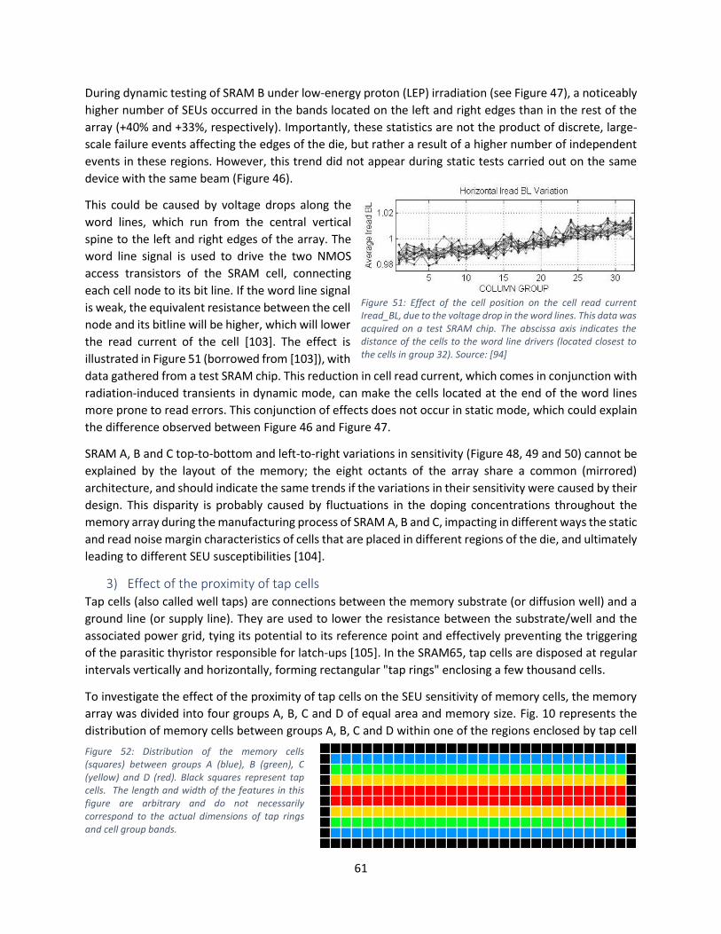
61
During dynamic testing of SRAM B under low-energy proton (LEP) irradiation (see Figure 47), a noticeably
higher number of SEUs occurred in the bands located on the left and right edges than in the rest of the
array (+40% and +33%, respectively). Importantly, these statistics are not the product of discrete, large-
scale failure events affecting the edges of the die, but rather a result of a higher number of independent
events in these regions. However, this trend did not appear during static tests carried out on the same
device with the same beam (Figure 46).
This could be caused by voltage drops along the
word lines, which run from the central vertical
spine to the left and right edges of the array. The
word line signal is used to drive the two NMOS
access transistors of the SRAM cell, connecting
each cell node to its bit line. If the word line signal
is weak, the equivalent resistance between the cell
node and its bitline will be higher, which will lower
the read current of the cell [103]. The effect is
illustrated in Figure 51 (borrowed from [103]), with
data gathered from a test SRAM chip. This reduction in cell read current, which comes in conjunction with
radiation-induced transients in dynamic mode, can make the cells located at the end of the word lines
more prone to read errors. This conjunction of effects does not occur in static mode, which could explain
the difference observed between Figure 46 and Figure 47.
SRAM A, B and C top-to-bottom and left-to-right variations in sensitivity (Figure 48, 49 and 50) cannot be
explained by the layout of the memory; the eight octants of the array share a common (mirrored)
architecture, and should indicate the same trends if the variations in their sensitivity were caused by their
design. This disparity is probably caused by fluctuations in the doping concentrations throughout the
memory array during the manufacturing process of SRAM A, B and C, impacting in different ways the static
and read noise margin characteristics of cells that are placed in different regions of the die, and ultimately
leading to different SEU susceptibilities [104].
3) Effect of the proximity of tap cells Tap cells (also called well taps) are connections between the memory substrate (or diffusion well) and a
ground line (or supply line). They are used to lower the resistance between the substrate/well and the
associated power grid, tying its potential to its reference point and effectively preventing the triggering
of the parasitic thyristor responsible for latch-ups [105]. In the SRAM65, tap cells are disposed at regular
intervals vertically and horizontally, forming rectangular "tap rings" enclosing a few thousand cells.
To investigate the effect of the proximity of tap cells on the SEU sensitivity of memory cells, the memory
array was divided into four groups A, B, C and D of equal area and memory size. Fig. 10 represents the
distribution of memory cells between groups A, B, C and D within one of the regions enclosed by tap cell
Figure 52: Distribution of the memory cells (squares) between groups A (blue), B (green), C (yellow) and D (red). Black squares represent tap cells. The length and width of the features in this figure are arbitrary and do not necessarily correspond to the actual dimensions of tap rings and cell group bands.
Figure 51: Effect of the cell position on the cell read current Iread_BL, due to the voltage drop in the word lines. This data was acquired on a test SRAM chip. The abscissa axis indicates the distance of the cells to the word line drivers (located closest to the cells in group 32). Source: [94]

62
rows and columns (black squares). Each group was made of a collection of horizontal bands, each a few
cells high and spanning the whole width of the memory array; group A contained only the memory cells
which were the closest to the taps, whereas group D contained the memory cells which were the furthest
away from them. Due to the simplicity of this partition scheme and to the layout of the taps, as illustrated
by Figure 52, groups B, C and D contain a small percentage of cells which are as close to a tap as the cells
in the A group, which are located next to the vertical boundaries of the tap ring. However, since the tap
rings are much wider than they are high, these cells are so few that they have a negligible impact on the
following statistics.
This partition scheme revealed that the distance of a memory cell to its closest tap cell had a clear impact
on its radiation sensitivity; the proportion of upsets occurring in each cell group is visible on Figure 53 for
static tests, and on Figure 54 for dynamic tests. These figures reveal that the positive correlation between
tap cell distance and memory cell sensitivity exists in the data from all test campaigns, but is significantly
stronger in heavy-ion data than in proton and neutron test data.
Figure 55 investigates further the impact of the
heavy-ion LET (or, in this case, species) on the
correlation between tap cell distance and memory
cell sensitivity. The correlation is found to be much
stronger when the device is irradiated with high-LET
ions: the difference in error count between groups
A and D is only 38% when considering tests with
nitrogen (LET 1.8 MeV.cm2.mg-1), but reaches 360%
during tests with xenon (LET 60 MeV.cm2.mg-1).
These results take into consideration both static
and dynamic test data.
The explanation for these correlations lies in the
structure of the “cloud” of free charge carriers
generated by the impinging ion; the size and
concentration of the carrier “cloud” depend on the
Figure 53: Effect of the proximity of the tap cells on the relative SEU sensitivity of memory cells (static test data). Heavy-ion data is shown in red, proton data in black, and neutron data in magenta.
Figure 54: Effect of the proximity of the tap cells on the relative SEU sensitivity of memory cells (dynamic test data). Heavy-ion data is shown in red, proton data in black, and neutron data in magenta.
Figure 55: Effect of the heavy-ion species on the relative sensitivity of the memory cell groups (mixed static and dynamic test data).
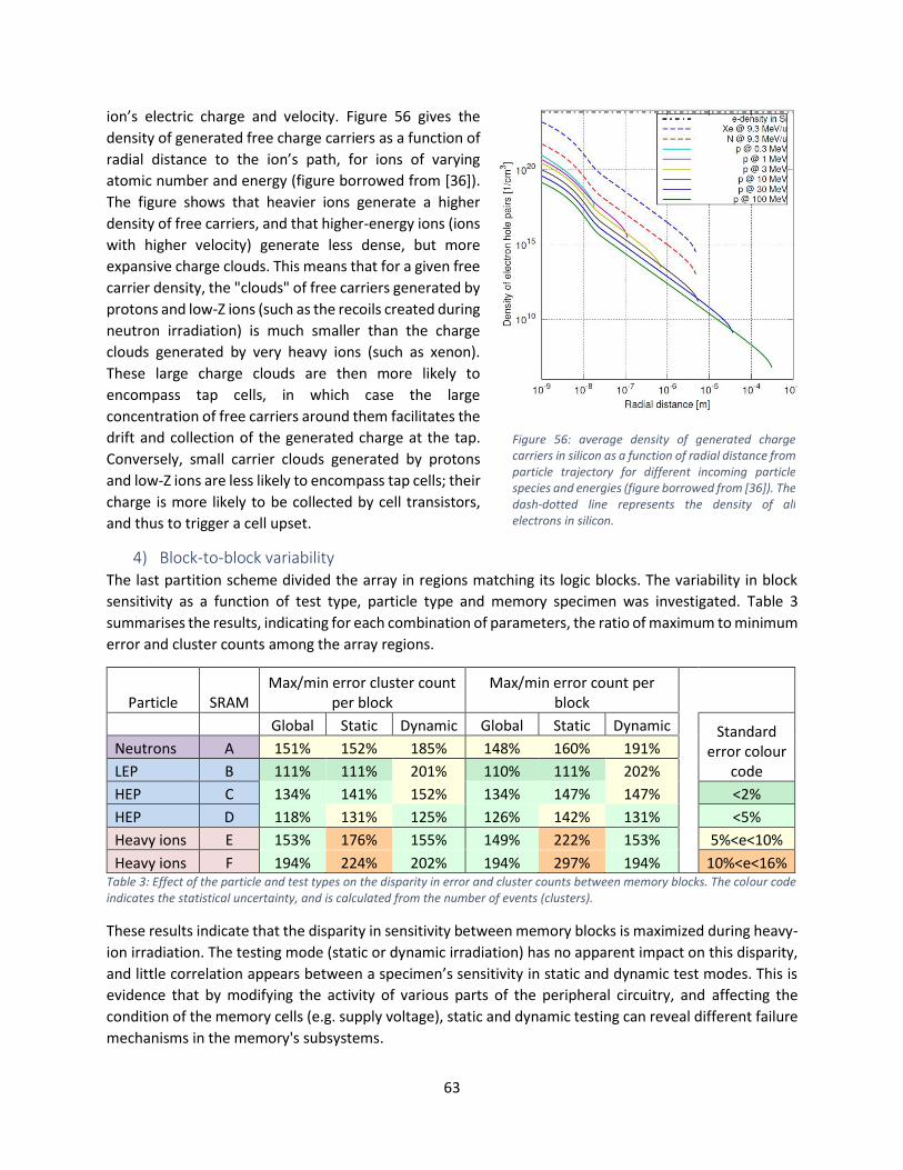
63
ion’s electric charge and velocity. Figure 56 gives the
density of generated free charge carriers as a function of
radial distance to the ion’s path, for ions of varying
atomic number and energy (figure borrowed from [36]).
The figure shows that heavier ions generate a higher
density of free carriers, and that higher-energy ions (ions
with higher velocity) generate less dense, but more
expansive charge clouds. This means that for a given free
carrier density, the "clouds" of free carriers generated by
protons and low-Z ions (such as the recoils created during
neutron irradiation) is much smaller than the charge
clouds generated by very heavy ions (such as xenon).
These large charge clouds are then more likely to
encompass tap cells, in which case the large
concentration of free carriers around them facilitates the
drift and collection of the generated charge at the tap.
Conversely, small carrier clouds generated by protons
and low-Z ions are less likely to encompass tap cells; their
charge is more likely to be collected by cell transistors,
and thus to trigger a cell upset.
4) Block-to-block variability The last partition scheme divided the array in regions matching its logic blocks. The variability in block
sensitivity as a function of test type, particle type and memory specimen was investigated. Table 3
summarises the results, indicating for each combination of parameters, the ratio of maximum to minimum
error and cluster counts among the array regions.
Particle SRAM Max/min error cluster count
per block Max/min error count per
block
Global Static Dynamic Global Static Dynamic Standard error colour
code
Neutrons A 151% 152% 185% 148% 160% 191%
LEP B 111% 111% 201% 110% 111% 202%
HEP C 134% 141% 152% 134% 147% 147% <2%
HEP D 118% 131% 125% 126% 142% 131% <5%
Heavy ions E 153% 176% 155% 149% 222% 153% 5%<e<10%
Heavy ions F 194% 224% 202% 194% 297% 194% 10%<e<16% Table 3: Effect of the particle and test types on the disparity in error and cluster counts between memory blocks. The colour code indicates the statistical uncertainty, and is calculated from the number of events (clusters).
These results indicate that the disparity in sensitivity between memory blocks is maximized during heavy-
ion irradiation. The testing mode (static or dynamic irradiation) has no apparent impact on this disparity,
and little correlation appears between a specimen’s sensitivity in static and dynamic test modes. This is
evidence that by modifying the activity of various parts of the peripheral circuitry, and affecting the
condition of the memory cells (e.g. supply voltage), static and dynamic testing can reveal different failure
mechanisms in the memory's subsystems.
Figure 56: average density of generated charge carriers in silicon as a function of radial distance from particle trajectory for different incoming particle species and energies (figure borrowed from [36]). The dash-dotted line represents the density of all electrons in silicon.
64
5) Summary A methodology for the investigation of radiation effects on memories was introduced, which is based on
error referencing, direct bitmap observation and database manipulation. When applied to the pool of
data acquired on the SRAM65, this method brought out further information from the radiation test data
than the typical SEE cross-section values, at no additional cost. Specifically, it highlighted specimen-to-
specimen variability due to manufacturing variations or silent defects, and topological trends in the
devices' SEU sensitivity due to their architectural features. The proposed methodology can be applied to
other types of memories than SRAMs.
The results from this study accentuate the need to systematically perform memory testing on several
specimens at once, to eliminate eventual device-specific biases in the test results. They also underline the
benefits of carrying out dynamic tests along with static tests during memory irradiation campaigns, as the
two test types bring out different failure mechanisms.
C. Muon-induced Single-Event Upsets in a 65 nm SRAM
In recent years, a few studies have shown that data corruption in SRAMs may occur from ionisation by
muons [106]; the abundance of these particles in the atmosphere raises the question of their impact on
the reliability of future devices built with further integrated technology. As discussed in Chapter 2, muons
have the same theoretical maximum electronic stopping power (or Linear Energy Transfer, LET) at the
Bragg peak as protons [107], [108], which means that they can induce a comparable amount of charge
per unit distance inside a memory component. The experimental static and dynamic SEU cross-sections
of the SRAM65 under low-energy proton and muon irradiation are discussed in a previously unpublished
study, the results of which were presented in [109].
1) Experimental setup Three devices from the same
manufacturing lot were exposed to an
antimuon (µ+) beam from the RIKEN-
RAL Port4 instrument at ISIS-RAL. The
particle fluence for each test was
chosen in accordance to the memories’
sensitivity, depending on the type of
test and muon energy, from 2.5∙107 up
to 3∙108 cm-2. The beam energies varied
from 1.99 MeV to 3.15 MeV. The
irradiation time varied from a few tens
of minutes (when the memory was the
most sensitive) to a few hours per run. A
schematic of the beam line setup is available on Figure 57. The beam dosimetry was obtained with a
scintillator positioned in front of the beam, while another pair of scintillators was used in line with the
target area to count the positrons emitted by the decaying antimuons after they stopped in DUT. The
uncertainty for the fluence in the beam dosimetry was given at +/-25%. The antimuon beam went through
a 50 µm mylar exit window, 20 µm of aluminium foil, a 300 µm polymer (polyvinyltoluene) scintillator,
and about 10 cm of air before reaching the chip.
Figure 57: Schematic of the Port4 antimuon beam line setup at ISIS.

65
The same SRAM device type was tested with low-energy protons at the RADEF facility (University of
Jyväskylä). The beam energies ranged from 0.6 MeV to 4.7 MeV. The particle fluence per test run varied
from 3.6∙106 to 3.6·107 cm-2 and the typical test duration was in the order of few minutes. The uncertainty
for the proton fluences in the beam dosimetry was given at ±10%. These irradiations were carried out in
vacuum.
Details about the combined deposited fluence and recorded upsets for each energy in the two test
campaigns are given in Table 4. Dynamic tests were not carried out for each energy.
2) Experimental results The response of the devices to antimuon and low-energy proton irradiations share similar characteristics.
Their sensitivity was much higher during the static tests than during the dynamic tests. This difference is
due to a power-saving measure, which consists in lowering the supply voltage of the memory array when
the memory is idle, and thus making the SRAM cell more sensitive to SEUs. Each proton test induced from
a few hundred to a few thousand upsets. This was also the case for the antimuon tests at which the initial
antimuon energy translated to peak ionization at transistor depth. The three devices tested at ISIS
Facility (beam)
Beam energy (MeV)
Total fluence, static
Total static upsets
Total fluence, dynamic
Total dynamic upsets
ISIS (antimuons)
1.99 5,75E+07 0 - -
2.19 9,27E+07 1500 1,28E+08 52
2.27 8,54E+07 1872 2,52E+07 24
2.35 4,68E+08 13200 6,53E+08 713
2.43 1,10E+08 2000 1,75E+08 123
2.48 1,57E+08 1788 6,89E+07 34
2.56 7,48E+07 162 2,76E+08 18
2.65 5,46E+07 50 - -
3.15 1,52E+08 13 - -
RADEF (protons)
0.6 3,63E+06 1461 2,89E+07 2886
0.98 7,22E+07 356415 2,53E+08 7835
2.2 3,61E+07 3993 1,44E+08 334
4.7 3,61E+07 238 1,44E+08 59
Table 4: Summary of the results of the test campaigns used in this study.
Figure 58: SEU cross-section per bit as a function of antimuon energy, for static tests. The colours differentiate the three test specimens, and the marker shapes differentiate the data pattern.

66
exhibited very closely matching cross-sections, which strongly depended on the initial antimuon beam
energy (which we define as the energy of the particles before they pass the beam exit window). Figure 58
presents the devices’ SEU cross-section data, obtained during static tests, as a function of antimuon
energy and data pattern.
The graph in Figure 60 presents the devices’ SEU cross-section during dynamic tests, as a function of
antimuon energy and dynamic test type. The response of the device tested at RADEF with low-energy
protons is given in Figure 59.
For the sake of clarity, the error bars are not displayed in the previous plots, but the uncertainty on the
cross-sections varied between ±27% and ±37% for antimuons. The uncertainty for proton cross-sections
ranged between ±12% and ±15%, except at 4.7 MeV where it ranges from ±30% to ±50%.
From a rough analysis of results, the maximum antimuon SEU cross-section is about two orders of
magnitude lower than the maximum proton SEU cross-section. Theoretically, the maximum electronic
stopping force of a given impinging particle is then given by its charge and its velocity, as discussed in
Chapter 2. All these parameters being equal for an antimuon and a proton, these particles should
theoretically have the same maximum electronic stopping force, although this would occur at different
energies because of their mass difference. However, in practice, this does not seem to translate
Figure 60: SEU cross-section per bit as a function of antimuon energy, for dynamic tests. The colours differentiate the three test specimens, and the marker shapes differentiate the type of dynamic test.
Figure 59: SEU cross-section per bit vs. proton energy. The square markers indicate static tests while the other markers dynamic tests.

67
experimentally into similar maximum SEU cross-sections. In the following section, this discrepancy will be
investigated with the help of Monte Carlo simulations.
3) Simulation results The interaction of antimuons and protons with the tested device structures was simulated with the help
of the Monte-Carlo Radiative Energy Deposition (MRED) code [110]. The geometry of the beam lines and
devices was modelled, which included the bulk silicon, and the oxide and metal layers of the DUT. In the
case of the antimuon simulations, the geometry also included the air, scintillator and various materials
placed in front of the DUT. A detector region was set to simulate the sensitive volume (SV), which
comprised the topmost 1 µm-thick layer from the active silicon substrate. Complementary cumulative
distribution functions (CCDF) of the particles’ LET in the SV were computed, for antimuons and protons,
with different initial particle energies (Figure 61 and Figure 62).
The CCDF plots indicate the probability (vertical axis) that an impinging particle has an LET (i.e. induces a
certain amount of charge carriers per unit length) equal or superior to a given threshold within the
sensitive volume (horizontal axis). These plots have been normalized to the proportion of particles which
effectively reach the DUT surface.
Figure 61: CCDF of the antimuon LET within the detector volume, for various initial beam energies. The dashed vertical line marks the critical LET used in the following analysis.
Figure 62: CCDF of the proton energy deposition within the detector volume, for various initial beam energies. The dashed vertical line marks the critical LET used in the following analysis.

68
Comparing these curves provides an insight on the different behaviour of antimuon and protons. Proton
LET CCDF curves start at a probability of 1, and then exhibit a clear elbow at an LET which depends on the
original proton energy. Beyond this point, the probability abruptly decreases. Because protons are heavier
than muons, there is less scattering in their trajectories due to interactions with the target electrons.
Results obtained with SRIM [55] simulations indicate that for the concerned energies, the proton range
longitudinal and lateral standard deviation is only about 5% of the average proton range.
Conversely, for low energies, the antimuon CCDF curves start at a probability lower than 1. This means
that at low energies, some of the antimuons which reach the surface of the DUT are stopped or
backscattered before reaching the sensitive volume. The antimuon CCDF curves also exhibit elbows, which
occur at a lower LET than for protons, but the following decrease in probability is not as sharp as for the
protons. For muon energies between 2 and 3 MeV, part of the CCDF curves extends into the region of high
energy deposition. This shows that, on average, within the SV, antimuons deposit much less energy than
protons, even though individual antimuons might deposit similar amounts.
The position of the elbow region of the CCDF curve is a good indicator of the probability to trigger an SEU
with a given particle at a given energy: the farther up and right the elbow is, the higher is the probability
of the particles having a high LET in the SV. According to this principle, the combined CCDF curves indicate
that the maximum SEU rate should appear around 2.4 MeV for antimuons and 0.6 MeV for protons, which
corresponds to the experimental observations (respectively 2.35 MeV and 600 keV).
The following analysis assumes that a memory cell’s SV is identical in the case of antimuon and proton
irradiation. If the occurrence of an SEU is determined by a particle depositing a critical charge in a SV, and
the cell sensitive volumes are identical in both cases, then it is possible to compare the SEU rates obtained
with antimuons and protons, as a function of this threshold LET value, by comparing the CCDF plots. By
varying the SEU threshold LET, and plotting the corresponding deposition probabilities from the LET CCDF
curves as a function of the incident particle energy, it is possible to study their effect on the predicted
relative SEU rate, as shown in the plot presented on Figure 63, for protons.
The simulated evolution of the SER as a function of proton energy best matches the evolution of the
experimental cross-section for an SEU threshold LET of about 0.24 MeV.cm2.mg-1. In Figure 64, a similar
plot is given for the antimuon experimental data. Figure 63 shows that at the peak proton cross-section
(600 keV), every particle which hits the SV releases enough energy to trigger an SEU, while (as seen on
Figure 63: Effect of the SEU threshold LET and proton energy on the predicted SEU rate. Different curves are used for different values of SEU threshold LET.
Figure 64: Effect of the SEU threshold LET and antimuon energy on the predicted SEU rate. Different curves are used for different values of SEU threshold LET.

69
Figure 64) at the peak antimuon cross-section, only about 2.5% of the particles which hit the SV do trigger
an upset. This explains the two orders of magnitude difference which has been observed between the
experimental proton and antimuon cross-sections.
4) Summary This study compared the response of the SRAM65 to low-energy proton and antimuon irradiation. A
difference of two orders of magnitude was found between the maximum experimental antimuon and
proton SEU cross-sections, despite the theoretically similar maximal particle LETs. Simulation results
performed with MRED clarified the experimental results: the lighter mass of antimuons (compared to
protons) results in stronger beam energy and range straggling, which leads to a lower effective SEU cross-
section at low energies. This means that proton testing methods may not be directly applicable to SEU
testing with muons; the strong energy straggling undergone by antimuons before reaching the DUT
sensitive volume should be carefully considered when designing an experiment, in particular on devices
with thick overlayers.
D. Failure mode analysis of an FRAM
As was mentioned in Chapter 3, Ferroelectric Random-Access Memories (FRAMs) store information as the
electric polarisation of ferroelectric capacitors. FRAM memory cells have shown extreme resilience to TID
[111] and SEE [112], and a high resilience to DD [113]. However, the memory array is controlled by
elements implemented in CMOS technology, which are vulnerable to radiation and may be the cause of
different types of failures. This section presents the results of an investigation into the failure modes of
the Cypress FM22L16 FRAM [114].
1) Experimental setup The FRAM device (see Chapter 6) was irradiated in several test campaigns, with heavy ions at RADEF
(Radiation Effects Facility, Univ. Jyväskylä, Finland) and GANIL (Grand Accélérateur National d’Ions Lourds,
Caen, France), and pulsed, focused X-rays at APS (Advanced Photon Source, Argonne National Laboratory,
Chicago, USA). The main characteristics of the beams are summarized in Table 5.
Facility DUT Test particle Energy Flux per run (cm-2.s-1)
Total fluence (cm-2)
GANIL #1 Heavy ions (Xe) 3.4 MeV/u, 13.2 MeV/u 4.0·102 to 7.0·104 1.7·106
RADEF #2 Heavy ions (Fe, Kr, Xe) 9.3 MeV/u 1.0·103 to 5.0·104 5.91·107
RADEF #3 Heavy ions (Kr, Xe) 9.3 MeV/u 1.0·103 to 4.0·105 7.7·106
RADEF #4 Heavy ions (Ne, Ar) 9.3 MeV/u 1.0·104 to 1.8·104 1.01·108
APS #5 Pulsed, focused X-rays 8 keV, 87pJ/pulse, 37 MeV.cm2.mg-1 equ. LET [115]
0.91 3.0·108
Table 5: Summary of the test campaigns used as a data source for this study.
DUT #5 was irradiated using beamline 20-ID-B at APS. The X-ray pulses delivered by the beam have a full
width at half maximum (FWHM) duration of 100 ps, and a FWHM spot size of 1.77 μm * 1.81 μm. The X-
ray energy was set at 8 keV; the attenuation lengths for the most common materials used in IC
manufacturing at this photon energy are presented in Table 6 (calculated with [116]).

70
The open-top DUT has about 5 μm of interconnecting and passivation
layers above the active silicon region [117]. We can estimate the
attenuation caused by these layers to be minor, since they are mainly
composed of SiO2, Al and Cu. Denser materials such as Sn and W are
typically used only for the lowest, thinnest interconnect layers and
connecting plugs, in small amounts, while TaN is used only as a thin
barrier layer between Cu and insulators.
Throughout this campaign, the total pulse energy at the DUT surface
was 87 pJ. In [115], a method has been developed to correlate the
transients resulting from the collection of charge carriers generated
by pulsed X-rays (using the same APS beam line) and heavy ions. Using
the coefficients and equivalence model described in [115], we can
calculate the equivalent LET of the X-ray pulses, LETeq:
𝐿𝐸𝑇𝑒𝑞 =1
𝑎𝐸𝑝𝑢𝑙𝑠𝑒(𝑏𝐸𝑝𝑢𝑙𝑠𝑒 + 𝑐) Equation 1
𝐿𝐸𝑇𝑒𝑞 =1
0.172×87×(1.16 · 10−4×87 + 7.4 · 10−2) Equation 2
𝐿𝐸𝑇𝑒𝑞 = 43 𝑀𝑒𝑉 · 𝑐𝑚2 · 𝑚𝑔−1 Equation 3
i.e. an X-ray equivalent LET of 43 MeV.cm2.mg-1 at the DUT surface. In the following discussion, we assume
an overlayer profile of 1.5 μm of Al, 1.5 μm of Cu and 3 μm of SiO2; this results in about 11% pulse energy
absorption between the DUT surface and the active silicon region [116]. The formula from [115] then
predicts a 37 MeV.cm2.mg-1 equivalent LET at the sensitive volume depth. The attenuation length in silicon
is so large (69.6 μm) compared to the typical dimensions of logic gates and register cells (a few square
micrometers) that for our purposes, we can consider the beam unattenuated once it reaches the silicon,
generating charge carriers in a long vertical column.
Several regions of the die have been selectively irradiated, to identify
the failure modes triggered by specific circuits. These included either
memory cells or parts of the central spine (a region of the die
containing peripheral circuitry, running across the memory array).
2) Bitmap generation The failure modes of the device were analysed with the use of bitmaps.
The bitmaps generated from the FRAM data are slightly different than
those generated for the SRAM devices. FRAM bitmaps are originally 64
pixels wide and 65536 pixels high; the resulting image is divided into 32
bands of equal lengths, which are laid out next to each other, to form
a square image. This means that FRAM bitmaps are read in a specific
manner, as indicated on Figure 65. These bitmaps have a black
background, and errors are indicated by coloured pixels; similar colours
identify errors which were detected on the same element and
operation of the algorithm. For ease of reading, the bitmaps are divided
into sectors by grey horizontal and vertical lines, which match the
height of some error cluster types (e.g. type 4, see Figure 67).
Material Density (g.cm-3)
α (μm)
Si 2.33 69.6
Si3N4 3.44 72.9
SiO2 2.2 130.4
Al 2.7 77.6
Sn 7.3 5.5
Cu 9.0 21.9
W 19.3 3.1
TaN 14.3 4.67
Table 6: Attenuation lengths α for 8 keV photons in materials commonly used in IC manufacturing.
Figure 65: Reading direction for FRAM bitmaps.

71
3) Experimental results The bitmaps revealed at least eight different failure modes:
• Type 1 events are 1-bit failures, which can be isolated errors (type 1a), or isolated errors occurring
at addresses related to (sharing many bits with) previous errors (type 1b). Type 1 events were
observed on all test campaigns, during both static and dynamic tests. (Figure 66)
• Type 2 events consist in several bits in one word being upset at once. The word may be either
partially corrupted (type 2a) or completely corrupted (type 2b). Type 2 events were observed on
all test campaigns, during both static and dynamic tests. (Figure 66)
Facility Device/DUT Ion Energy (MeV)
LET@surface (MeV.cm2.mg-1)
Tilt angle (degrees)
Flux (counts.s-1.cm-2)
Fluence (counts.cm-2)
Test type Addressing
RADEF FRAM/3 Kr 768 32.1 0 5.0·103 3.0·105 Dynamic stress Anti-Gray
Figure 66: Logical bitmap from an anti-Gray dynamic stress test with krypton (LET 32 MeV.cm2.mg-1).

72
• Type 3 events consist in several pages with the same page number (appear at the same height
within their logical bitmap sectors) showing large numbers of upsets affecting several words. Type
3 errors were only observed on heavy-ion campaigns, and only on dynamic tests. (Figure 67)
• Type 4 events consist in one particular bit of every page within a logic sector suffering either
intermittent errors (type 4a) or continuous errors (type 4b), resulting in an interrupted or
continuous vertical line on the chronological bitmap. In addition, sparse single-bit upsets (SBUs)
may occur randomly within the affected sector. Type 4 events were observed on all test
campaigns, mostly on dynamic tests. (Figure 67)
Facility Device/DUT Ion Energy (MeV)
LET@surface (MeV.cm2.mg-1)
Tilt angle (degrees)
Flux (counts.s-1.cm-2)
Fluence (counts.cm-2)
Test type Addressing
RADEF FRAM/3 N 139 1.8 0 3.0·105 1.2·107 mMATS+ Natural
Figure 67: Logical/chronological of a natural addressing mMATS+ test with nitrogen (LET 1.8 MeV.cm2.mg-1).

73
• Type 5: the chronological bitmap on display on Figure 68 was gathered during an anti-Gray
dynamic stress test on DUT #4. It exhibits, among type 1 and 2 events, two small blocks of errors
in the top left corner; each block is made of 38 completely upset words. A closer examination of
the data logs reveals that each of these 76 addresses actually returned errors on several
occasions, during two consecutive element scans of the Dynamic stress algorithm. During the first
element scan, after the w0 operation, the five consecutive r0 operations all failed on each of these
addresses; then, on the next element scan, the first operation, r0, failed on all these addresses.
Subsequent accesses to these memory locations returned no errors for the rest of the test.
Facility Device/DUT Ion Energy (MeV)
LET@surface (MeV.cm2.mg-1)
Tilt angle (degrees)
Flux (counts.s-1.cm-2)
Fluence (counts.cm-2)
Test type Addressing
RADEF FRAM/4 Ar 372 1.17 30 1.3·104 1.0·106 Dynamic stress Anti-Gray
Figure 68: Chronological bitmap of an anti-Gray dynamic stress test with argon at 30° (LET 11.7 MeV.cm2.mg-1).

74
The logical bitmap for this test run is available on Figure 69. This figure shows how all the errors
visible on the chronological bitmap in Figure 4 have closely related addresses (they are close to
each other on the logical bitmap). Type 5 failures are rare: they were only reported once, during
this heavy-ion test on DUT #4.
• Type 6 events consist in several hundred consecutively-accessed words being either completely
upset (type 6a), or completely upset except for a few occasional bits (type 6b). The colored blocks
appearing on Figure 70 are type 6a events. The number of words affected by type 6 failures seems
Facility Device/DUT Ion Energy (MeV)
LET@surface (MeV.cm2.mg-1)
Tilt angle (degrees)
Flux (counts.s-1.cm-2)
Fluence (counts.cm-2)
Test type Addressing
RADEF FRAM/4 Ar 372 1.17 30 1.3·104 1.0·106 Dynamic stress Anti-Gray
Figure 69: Logical bitmap of an anti-Gray dynamic stress test with argon at 30° (LET 11.7 MeV.cm2.mg-1). This bitmap contains the same data as that visible on Fig. 18, and the zoom-in identifies the errors highlighted in the zoom-in of Fig. 18. The complex pattern is caused by the complex anti-Gray addressing used for this test.

75
to be directly influenced by the type of dynamic test, and more precisely, by the speed at which
the algorithm scans across the address space. Figure 70 exhibits several type 6a events, each
affecting about 350 words. The data for this figure was gathered during an mMATS+ test; the
elements of this algorithm contain two operations each. The data used for Figure 71 was gathered
on the same DUT in exactly similar conditions, except that the test algorithm was Dynamic Classic,
whose elements only contain one operation – meaning that the Dynamic Classic algorithm scans
addresses faster. Figure 71 also exhibits several type 6a events, but in this case each event affects
about 770 words. This correlation between algorithm scanning speed and type 6 event severity
was verified on tens of different test runs; it indicates that type 6 events last for a constant amount
of time (or a constant amount of I/O operations).
Type 6 events were observed only on heavy-ion campaigns, dynamic tests only.
• Type 7 events involve several thousands to tens of thousands of consecutively-accessed words,
which exhibit a high density of random upsets, generating hundreds of thousands to millions of
upsets. The device may eventually recover from the condition spontaneously. The type 7 event
visible on Figure 72 is the logical/chronological bitmap from a pulsed X-ray test on DUT #5 at APS.
The beam scanned a region of the central peripheral spine, while a natural-order mMATS+
dynamic test was performed. This type of SEFI also occurred during heavy-ion dynamic testing.
Facility Device/DUT Ion Energy (MeV/u)
LET@surface (MeV.cm2.mg-1)
Tilt angle (degrees)
Flux (counts.s-1.cm-2)
Fluence (counts.cm-2)
Test type Addressing
GANIL FRAM/1 Xe 3.43 64.3 0 5.0·102 1.0·105 mMATS+ Dynamic classic
Natural
Figure 70: Logical/chronological bitmap obtained from an mMATS+ test with xenon (LET 64.3 MeV.cm2.mg-1).
Figure 71: Logical/chronological bitmap obtained from a dynamic classic test with xenon (LET 64.3 MeV.cm2.mg-1).

76
• Type 8: several thousands to tens of thousands of words are either entirely, or almost entirely
corrupted; these words all have a few address bits in common. This is evidenced by the fact that
on a logical bitmap, the errors generated by type 8 events fill up entire binary subdivisons of the
bitmap – either the whole bitmap, or one half, or one or more quarters or eighths, etc. This is
evident on Figure 73, where a type 8 event takes up a whole eighth of the bitmap. Since this is a
logical bitmap from a natural-addressing test, it means that the type 8 event started as the third
Facility Device/DUT Ion Energy (MeV)
LET@surface (MeV.cm2.mg-1)
Tilt angle (degrees)
Flux (counts.s-1.cm-2)
Fluence (counts.cm-2)
Test type Addressing
RADEF FRAM/4 Ar 372 1.17 30 1.3·104 1.0·106 Dynamic stress Anti-Gray
Figure 72: Logical/chronological bitmap obtained from an mMATS+ test with pulsed X-rays aimed at the central peripheral spine of DUT #5 (equivalent LET 37 MeV.cm2.mg-1).

77
most-significant address bit toggled from 0 to 1, and ended as soon as it toggled back to 0. This
type of event was recorded on all heavy-ion test campaigns, but on dynamic tests only. Type 8
events were also detected on dynamic tests where the addressing was not natural – for example,
anti-Gray. This means that the errors which appear during a type 8 event are not necessarily
accessed consecutively.
Facility Device/DUT Ion Energy (MeV)
LET@surface (MeV.cm2.mg-1)
Tilt angle (degrees)
Flux (counts.s-1.cm-2)
Fluence (counts.cm-2)
Test type Addressing
RADEF FRAM/3 Kr 768 32.1 0 5.0·103 3.0·105 Dynamic stress Anti-Gray
Figure 73: Logical bitmap from a natural Dynamic Classic test with krypton (LET 32.1 MeV.cm2.mg-1).

78
Several noteworthy events occurred during static heavy-ion tests on DUT #2. The memory was written
with a known data pattern (every word contains the lower 16 bits of its address vector) and irradiated
under bias, then read back. On a few occasions, with iron, krypton and xenon beams, the readback data
contained a few words with erroneous data (type 2a errors). These errors can be considered permanent,
since subsequent readbacks returned the same errors. However, they disappeared after power cycling
the DUT.
Similar events occurred during a static test on DUT #5, with the X-ray beam aimed at the central spine.
The device was written with a known data pattern, then irradiated. When read back after the irradiation,
two type 2a events were detected at unrelated addresses. These two words were marked by overwriting
a specific data pattern (0xABCD), after which the device was power cycled, and read back again: the
readback data were correct at all addresses, except from the two words, which previously underwent a
type 2a event (they did not contain 0xABCD anymore). These two words were written with 0xABCD again,
the DUT was power cycled again, after which the memory performed as expected.
4) Discussion These different failure modes suggest the occurrence of faults in several different elements of the
peripheral circuitry.
Type 1 and 2 SEEs were detected both in static and dynamic modes, both during heavy-ion testing and X-
ray periphery attacks, but never during X-ray FRAM cell attacks, thus their origin must lie in the peripheral
circuitry. These events never occurred when the memory was irradiated in a powered-off state. Errors
disappear after a power cycle; however, if new data are written to a corrupted word before cycling power,
these data will change after the power cycling. This indicates that the element of the periphery which is
upset by radiation is restored in its correct state during device power-on boot. One potential cause of
these SEE could be upsets occurring in SRAM-based redundancy registers, whose purpose is the
reallocation of faulty memory elements (rows, columns, blocks) to spare elements within the memory
array. Upsets in such registers will be latched and trigger errors until they are reinitialized to their correct
value. These registers are always reloaded with correct values at device power-on.
Type 4 SEE: the facts that this type of event occurred during X-ray periphery testing, and that most of the
errors generated occur at the same bit of the same word within their page suggest two possible fault
mechanisms. The first hypothesis is an upset of a redundancy register, with the consequence of either
reallocating a functional column to a spare column (thus not correctly initialized), creating a continuous
4b event; or the re-allocation of a spare column to a malfunctioning column (not supposed to be used),
or the allocation of a functioning column to a malfunctioning spare (not supposed to be used), resulting
in an intermittent 4a error. The second hypothesis is the occurrence of a micro-latchup event or a stuck
bit in a page buffer. Such events induce metastability in the buffer cells, explaining the occurrence of
seemingly random errors occurring concurrently to the “vertical lines” in the rest of the page buffer
positions during type 4 events (see Figure 67).
Type 3 SEE: these events could have similar origins to those of type 4 events. Since the affected pages
share similar page numbers, they could all be part of a single memory row which was reallocated to a
spare row. Another possibility would be that an element common to these pages (e.g. a low-level address
decoder) was disturbed during the test.

79
Type 5 SEE: the addresses involved in this event started returning all-corrupted words after a w0
operation. For each of these addresses, several read operations spread over two scanning cycles returned
the same result, until their cells were eventually rewritten. This failure can be explained by a temporary
stuck address bit. Typically, during an access to the memory, the value input on the memory’s address
pins is loaded into an address buffer. If, under the effect of radiation, one or more bits from the buffer
get stuck, then the requested operation will be performed at the wrong memory location. This hypothesis
is supported by the chronological bitmap on Figure 68, which indicates that during the event, in
chronological order, every other address accessed failed. This is consistent with the fact that all address
bits -but one- toggle from one access to the next in anti-Gray addressing mode: the stuck bit fault can only
trigger errors on every other position accessed.
Another explanation for this event could be a failure of the write operation of the first element of the
algorithm. As indicated by Figure 69, all the words involved in this event have related addresses, which
means that there is a high probability that they share common read/write control circuits. It is possible
that locally, the peripheral elements required for write operations were temporarily disabled by an ion
strike. This hypothesis is supported by the fact that no other large group of errors is visible on the logical
bitmap.
Type 7 events are large-scale functional interrupts, which do not affect an “even” amount of words (a
power of 2), seemingly start and stop at random address positions, and trigger a pseudorandom output,
could originate in an upset of device configuration registers, or in a micro-latch-up affecting peripheral
elements. Micro-latch-up conditions have been shown to disappear spontaneously in CMOS devices,
when the high voltage lines sustaining them are switched off as part of normal device activity [98].
Type 8 events are large-scale failures which affect an “even” amount of words (a power of 2). They begin
and end when certain address bits toggle; since each address bit controls one level of address decoding,
type 8 events must be “mapped” on the memory array. For example, the type 8 event visible on Figure 73
affected exactly one eighth of the memory array; since the memory array is organized in eight blocks, one
possibility is that a radiation-induced upset in a configuration register disabled a critical element in one of
the eight memory blocks – and that subsequent accesses to this memory block returned an erroneous
value. Since three address bits are used to select blocks, the type 8 event started when the lowest-level
block-selecting bit toggled, and ended when another block was selected at the next toggle. Possible origins
for these events could be upsets in configuration registers (e.g. controlling power switches feeding
memory blocks).
This study shows that the SEE occurring in the FM22L16 come in several types, with different root causes,
of different magnitudes and severity. All these SEEs can be considered to originate in the peripheral
circuitry, as also suggested by previous studies [117][118]. However, experimental data show that at least
some categories of SEE (notably type 2 errors) can be avoided by forcing a reset of the involved peripheral
elements via power cycling the DUT before access (and possibly via putting the device out of sleep mode).
This has major implications regarding the device’s radiation sensitivity, since type 2 events are by far the
most frequently encountered. Many applications using the device as a storage memory could easily
implement systematic power cycling before device access as an error mitigation technique.
The results of this study suggest that hardening key elements of the peripheral circuitry of a memory
device (e.g. implementing the registers with additional transistors [119] or a dual-interlocked cell
architecture [120]) could effectively mitigate the most common failure modes. This would dramatically

80
improve the failure rate of the device, at the expense of a small increase in the area of the peripheral
circuitry.
E. Effects of heavy-ion radiation on a Single-Level Cell NAND flash memory
The study presented in this section was driven by the MTCube project [21][22], which calls for a 1-Unit
CubeSat to expose several types of memories fabricated with both legacy and emerging technologies to
space radiation, including the Micron flash memory. These results were also published in V. Gupta’s 2017
doctoral thesis dissertation [123]. Several different failure modes were observed after static heavy-ion
irradiation.
1) Experimental setup Two test campaigns were conducted, as summarized in Table 7. All tests were carried at normal beam
incidence angle with respect to the die surface.
The first test campaign was carried out at GANIL [124] in Caen, France on two specimens. The primary
xenon beam was degraded to reach a LET of 26.75 MeV.cm².mg-1 at the surface of the DUT. The tests were
performed in air. The second test campaign took place at the RADEF facility [125] at the University of
Jyväskylä, Finland. Tests were carried out on two specimens in vacuum, with beams yielding LETs of 1.8
to 60 MeV.cm².mg-1.
The fluence ranged from 1.0 × 10⁴ to 1.5 ×105 cm-² for each individual test, during both irradiation
campaigns. As for static buffer testing (at RADEF only), the fluence ranged between 6.2 ×10² and 1.0 × 10⁵
cm-² per test. At both facilities, the beam homogeneity was estimated to be +/- 10% or better over the
device area.
Test campaign Ion Energy (MeV)
Effective LET (@ surface) (MeV/(mg/cm2))
Range (μm)
GANIL Xe 46.55 26.8 700
RADEF N 139 1.8 202
Fe 523 18.5 97
Kr 768 32.1 94
Xe 1217 60.0 89
Table 7: Heavy-ion cocktails used at the different facilities. The values were provided by the facilities.
The memory devices were tested under two different test modes: the static (or retention) mode, and the
static buffer mode. The DUTs were biased during irradiation. Due to the very large capacity of the memory,
only 512 Mib (64 blocks) out of 32 Gib were considered for the static tests.
In static buffer mode, instead of reading the memory normally, one page (64 kib) was loaded, so that its
contents were stored on the memory data buffer; then the sequence of commands to carry out a reading
operation was interrupted, and the DUT was irradiated; finally, the reading operation was completed to
check the contents of the buffer.
Several operations (Erase, Write, Read) were performed in between runs, before and after Power Cycles
(PC), to observe the errors occurring during the test runs and to ensure that the device was error-free
prior to the next run.

81
2) Experimental results and discussion
Static mode tests
Static tests performed with nitrogen resulted in respectively 1 and 2 SBU (Single-Bit Upset within a word)
when using the solid ‘0’ pattern at a respective fluence of 3.0·104 and 1.5105 cm-². At those levels of
fluence, no errors were recorded when using the solid ‘1’ pattern. An erase operation was sufficient to
correct the SBUs without the need of a PC.
Irradiation results with the other heavy-ion particles resulted in widely varying numbers of erroneous
words per test, requiring a deeper analysis. Besides counting the number of erroneous words, the number
of upset bits was evaluated for each word presenting error(s), and logical bitmaps were generated. The
bitmaps of the Flash memory are built as follows: the left half of the bitmap contains the even blocks,
while the right half contains the odd blocks (accordingly with the manufacturer datasheet). Each block is
made of 128 horizontal lines, which each corresponds to a page. Each line is made of 8192 pixels, one per
column – each column holding one memory word. The individual bits of each word are not represented
on the bitmap. The two planes of the memory (halves of the bitmap) have their own data buffer. Due to
the very large size of the generated bitmaps (over 64 million pixels each), it is not possible to clearly display
them entirely, hence only their most relevant sections will be exhibited to support the test results analysis.
Regular patterns of errors were observed such as Vertical Lines (VLs) of errors, as well as small clusters of
words or isolated words with errors.
For each run, histograms were plotted, displaying the total count of word errors for each column on the
64 memory blocks which were tested. An example of a histogram is shown in Figure 74. The leftmost plots
Figure 74: Histogram of a static test bitmap, where the number of word errors (ordinates) is plotted for each column (abscissa). The two leftmost (resp. rightmost) plots represent the plane containing the even (resp. odd) blocks. The bottom histograms represent the error counts after removing the VLs. Each plane contains 4096 x 8192 words.

82
represent one plane (odd blocks), the rightmost plots represent the second plane (even blocks). The top
plots represent the total number of word errors per column while the bottom plots are similar the
previous ones, but they do not display the columns which suffered too many word errors (the threshold
was arbitrarily set to 64), allowing filtering the vertical lines of errors from smaller clusters. Thanks to this
filtering, it was possible to plot the memory cross-section while only considering the small clusters of
errors.
Two categories of failures could be identified on the bitmaps:
Vertical Lines (VL) - For a large majority of plotted bitmaps, the most significant error types that appeared
were VL of errors, running from the top to the bottom of the bitmap and crossing all blocks either in the
left plane (even blocks) and/or in the right plane (odd blocks) ().
Several VLs may occur during one test, at any position in the planes. The threshold LET for the appearance
of VLs is between 1.8 MeV.cm²/mg (N ions) and 18.5 MeV.cm²/mg (Fe ions). The vertical lines are
sometimes continuous, with all words of the column exhibiting bit errors, and sometimes discontinuous,
with sparse word errors along the column, as shown on Figure 75: Close-up on a small region of a bitmap
generated after static mode tests, where two types of VLs are visible (continuous and intermittent). Words
are shown as black pixels if they exhibit bit errors, and as white pixels otherwise. The grey horizontal lines
are used to highlight the boundaries between blocks and do not represent errors.Figure 75. They were
observed on every test run in static mode (solid ‘1’, solid ‘0’, checkerboard and anti-checkerboard data
background patterns), on three specimens tested in two different test facilities (except when tested with
nitrogen, 1.8 MeV.cm²/mg).
Erase operations do not suppress VLs, neither does power cycling (PC) the device - only the combination
of a PC followed by an erase operation removed the errors. The VLs appeared to be dependent on the
data background pattern: after beam exposition, writing and reading ‘all 0’ always gives VLs at the same
positions, while writing and reading ‘all 1’ always returns another, separate set of VLs.
Figure 75: Close-up on a small region of a bitmap generated after static mode tests, where two types of VLs are visible (continuous and intermittent). Words are shown as black pixels if they exhibit bit errors, and as white pixels otherwise. The grey horizontal lines are used to highlight the boundaries between blocks and do not represent errors.

83
Two failure mechanisms are proposed to explain the occurrence of these VLs of errors:
• A stuck bit in the data buffer. During a block read operation, pages are loaded in the data buffer,
one at a time, to be serially transmitted out of the memory. If one bit of the data buffer is stuck
to a given value, which is the opposite of the value stored in the memory (e.g. stuck to ‘1’ when
‘all 0’ is stored in the memory), at each page read, the same error will appear at the same position
in the data buffer. Since the pages are represented by horizontal lines of pixels, the errors appear
at the same position on each horizontal line of the bitmap, creating a VL of errors. This failure
mechanism can explain the shape and extent of the VLs, but it cannot explain the fact that to stop
this behavior, an erase cycle is necessary, as the erase action does not affect the data buffer.
• The control electronics of the failing bit line. If the failure is not due to the data buffer, it must be
caused by a fault in the bit line control logic, since particles cannot directly upset hundreds of cells
at once, in this specific arrangement. Specifically, it must involve one of the elements involved in
the sensing action of the read operation. For example, in the event of a particle hit which would
generate a large amount of charge, the concurrent effects of a triggered micro-latchup and
charges trapped in the bit line access transistor [126] result in partial or total inhibition of the
access to the bit line. All accesses to the column will be affected, generating a VL. To stop the
failure condition, it is necessary to carry out both a PC, removing the micro-latchup, and the erase
operation that restores the access transistor.
Isolated MBUs and clusters of MBUs - Besides the VLs, isolated MBUs
(Multiple Bit Upsets within the same word) were also observed along with
small clusters of MBUs (two to five) lined up vertically (i.e. along the same
bit lines), at contiguous line addresses. No diagonal nor horizontal cluster of
errors was detected. These errors occur randomly across the entire bitmap.
Examples of such error types are depicted in Figure 76. An interesting
characteristic of these clusters of MBUs is that the failing bits are generally
the same among the words of a single cluster. After a PC, the number of
erroneous bits in each word was reduced to one (SBU). This is an important
point for applications, since power cycling the device before reading sensitive data could be a means to
mitigate errors. These PCs do not accelerate the aging of the cell like erase actions do, and reducing to
one the number of faulty bits allows the use of efficient error detection and correction techniques.
Isolated MBUs and clusters of MBUs occurred only for solid ‘0’ data background tests and never for solid
‘1’ tests. This is in line with previous results, such as those reported in [127], stating that during beam
irradiation, floating gate cells are more resilient to bit flips when storing a ‘1’ (floating gate with no charge)
than when storing a ‘0’ (charged floating gate). These errors can all be removed by an erase operation,
which discharges the floating gate, whereas a PC does not; reading the device after a PC returns about
the same number of word errors, with a small fluctuation. These fluctuations are due to borderline cells,
i.e. cells with their floating gates at an intermediate potential after irradiation, which makes the result of
a read access uncertain (intermittent errors) [126]. These small error clusters occurring along the bit line
with similar error patterns can be explained by the action of a single particle hitting the memory plan.
Charge sharing can also possibly occur, leading to several bits being upset in a single word. Secondary
particles generated at angles may also be the cause of these vertical clusters, considering that spacers
separate the columns and mitigate horizontal clusters.
Figure 76: Close-up on error clusters taken from a bitmap generated after static mode tests, showing the shape and size of single word errors or small cluster of errors.

84
Static buffer mode tests
Irradiation at a LET of 1.8 MeV.cm2.mg-1 resulted in no buffer errors, whether using the checkerboard or
solid ‘1’ pattern. Conversely, using ions with a surface LET of 18.5 MeV.cm2.mg-1 or higher, all runs
returned in errors. The SEU LET threshold of the data register is somewhere between these two values.
The results from these runs can be classified into two groups:
• For some runs, few errors were detected (between 12 and 40 failing words). Generally, the failing
words had only one single bit upset, although a few MBUs occurred;
• Other runs resulted in the entire data buffer (8192 words) failing. These events occurred twice
out of three runs at a LET of 18.5 MeV.cm2.mg-1, and once out of three runs at 60 MeV.cm2.mg-1.
When all words failed, and the buffer was loaded with a checkerboard, each word tended to have
4 bit failures, whereas when it was loaded with a solid ‘1’ pattern, every bit of every word failed.
When considering the tests of the first group only, the word cross-section follows a Weibull curve, as
depicted in Figure 77.
Similar experiments testing the data register were made by [126] on another NAND Flash component,
which gave a cross-section an order of magnitude lower than evidenced by our tests.
Regarding the runs with a fully faulty buffer, the fact that most words have 4 bit errors using the
checkerboard pattern, or 8 bit errors using a solid ‘1’ pattern, suggests that during the irradiation, the
control logic ruling the reset function of the data buffer produced unwanted resets and all bits were set
to ‘0’. The datasheet of the memory indicates that a reset command to clear the data register exists,
supporting this assumption. In these cases, the few words containing odd number of bit upsets are simply
the result of direct SEUs occurring in the buffer after the reset; the closer the faulty reset is to the end of
the irradiation, the more regular the error pattern is, with 8 bit flips for solid ‘1’ data background and 4
bit flips for checkerboard background.
3) Conclusion This study investigated the heavy-ion response of an SLC NAND flash memory in static mode. The observed
errors can be classified into three groups: vertical lines (VLs) of errors (continuous or discontinuous), small
vertical clusters of word errors, and single word errors. The VLs most likely occur in the bit line control
Figure 77: Word cross-section of the data buffer calculated by dividing the number of failing words by the fluence and the buffer size (8192 words). The LET threshold was set at 2 MeV.cm2.mg-1 to fit the data with a Weibull curve. The Weibull parameters are: W = 31.10, S = 2.78, σsat = 1.14·10-6 cm²/byte, LETth = 2.0 MeV.cm².mg-1

85
circuitry due to latch-up or stuck bit phenomena, while the other two types of errors are due to direct
ionization of the memory cells. Static tests of the data buffers allowed the determination of their
sensitivity, as well as the detection of unwanted reset events. The identification of these different failure
modes permitted to optimize the test program of the MTCube payload.
F. Single-Event Latch-ups in an MRAM
Similarly to FRAMs, Magnetoresistive Random-Access Memories, or MRAMs, are an emerging type of non-
volatile memory devices. This technology has the potential to bring together the endurance, performance
and low power consumption of SRAMs with the low cost and high density of flash memories. MRAM cells
are based on magnetic tunnel junctions, which are immune to SEEs and TID effects (see Chapter 3).
However, as is the case with the FRAM previously discussed in Section D, the periphery of these circuits is
implemented in CMOS and is sensitive to radiation.
A 3D component (several devices stacked in a single package) based on a toggle-MRAM device from
Everspin Technologies (see Chapter 6) was selected to be flown on the RES experiment. The standalone
MRAM device was the subject of multiple radiation test campaigns during the development of the
payload, and was found to be prone to suffering from Single-Event Latch-ups (SELs, see Chap 5). The
findings of these test campaigns have not yet been published, and will be briefly summarized in this
section.
Seven devices from three different manufacturing lots were irradiated over the course of five campaigns
at RADEF and GANIL, with ions ranging from nitrogen to xenon, in static and dynamic modes. A summary
of the beams used in this study is available in Table 8. According to the MRAM datasheet, the maximum
supply current at VDD=3.6 V is 68 mA during read mode, and 180 mA in write mode. These values are
influenced by the operating conditions, though, and at the frequency used during our tests (7 FPGA clock
cycles at 50 MHz, or 140 ns per read cycle) and with a bias voltage of 3.3 V, the typical supply current level
was 4.3 mA in standby, and 11 mA in dynamic stress tests. However, at power-up, the device briefly sinks
several tens of mA; to ensure proper device operation, the compliance level of the delatcher board was
set at 180 mA during the MRAM SEL tests.
While none of the DUTs were sensitive to nitrogen (at any angle) or to neon at normal incidence (LET 3.6
MeV.cm2.mg-1), SELs were observed with neon at 45° (LET 5.1 MeV.cm2.mg-1) and with all ions yielding a
greater LET. The MRAM’s threshold LET for SEL occurrence is somewhere between these two values.
The MRAM’s supply current was affected by events of two types:
Table 8: Summary of the beams used for MRAM SEL characterization.
Test campaign Ion Energy (MeV)
Angles (degrees)
Effective LET (@ surface) (MeV/(mg/cm2))
Range (μm)
GANIL Xe 3.4 to 46.6 0 64.3 to 26.8 37 to 700
RADEF N 139 0 to 45 1.8 to 2.5 202
Ne 186 0 to 45 3.6 to 5.1 146
Ar 372 0 to 50 10.1 to 1.6 118
Fe 523 0 to 45 18.5 to 26.2 97
Kr 768 0 32.1 94
Xe 1217 0 60.0 89

86
• “Current excursions”, which were only observed in static mode. During these events, the DUT’s
supply current abruptly increases a few milliamps above its typical idle value (4.3 mA) and remains
constant. After a few seconds to a few minutes, the DUT recovers spontaneously (sometimes
while still under irradiation) and the supply current returns to its initial value (Figure 78).
• SELs, which were observed in both static and dynamic modes. During SELs, the current increases
abruptly by a few tens to a few hundreds of milliamps; from then on, the DUT never recovers from
the condition until power is cut off. Very often, the supply current keeps increasing in successive
steps of a few tens to a few hundred milliamps, until the DUT is destroyed by thermal runaway,
or the power supply reaches its compliance value (see Figure 79).
Figure 78: Examples of supply current fluctuations during current excursions. All the data was gathered on the same DUT, during static irradiation with argon ions at an angle of 0° (curve #1) and 45° (curves #2 and #3). The beam flux was about 104 counts.s-1 at the DUT surface.
Figure 79: Examples of supply current fluctuations during SELs. The data was gathered on the same DUT for curves #1 and #2, and on a second DUT for curve #3, during static irradiation with iron ions at a normal incidence. The beam flux at the DUT surface was about 1.5·104 counts.s-1 for curves #1 and #2, and about 103 counts.s-1 for curve #3. The compliance level of the power supply used to power the DUTs was always set at 400 mA.

87
The cause for the observed current excursions could be logic conflicts (e.g. bus contention).
MRAM SEL currents have been observed above 800 mA for 60 s, and up to 1 A for 10s, without
causing any noticeable damage, idle current increase or data corruption in the DUT. (It must
be noted that at these current levels, the voltage drop across the DUT power cables was very
significant, but was not measured. Hence, the bias voltage of the DUT during these SEL events
is not known.)
Conversely, one 400 mA SEL event has been found to cause permanent damage in one of the
DUTs irradiated with iron at normal incidence. A zoom-in of a logical bitmap from a blank test
(no irradiation) carried out just after this hard SEL is available on Figure 80 (MRAM bitmaps
are read like an FRAM bitmap; see Section D). Two such regions were visible on the whole
bitmap (which cannot be clearly displayed entirely, at 16 million pixels), which means that a
region of the array containing 16,384 words, representing 131,072 bits, suffered permanent
damage because of the SEL. All these words suffer from intermittent failures on their most
significant bit.
Some memory devices – mostly SRAMs - store bits of similar weight together, in dedicated
regions of the die; this architecture helps mitigate MBUs [128]. The failure visible on Figure 80
could be explained by e.g. an SEL damaging a read element common to all the cells of a 16,384-
bit memory block containing the MSBs of 16,384 words. However, the author does not know
whether the MRAM uses this architecture, and this could not be determined from
photographs of the die.
Another possible explanation could be the depolarization of the free layer of the MTJ [129]
and/or other elements of the affected cells by the magnetic fields generated by the SEL
currents. The intense SEL currents (up to several hundred milliamps), which are generated
within the die, close to the memory cells, can generate considerable magnetic fields.
Theoretically, a pristine MRAM device – benefitting from its built-in magnetic shield – can be
upset by a magnetic field of 8000 A/m [130], which corresponds to the field generated by a
400 mA current at a distance of 8 μm [131]. In the present case, however, the devices were
delidded, which means that their magnetic shielding layer was removed. Without magnetic
shielding, it is probable that a 400 mA current would generate a magnetic field high enough
to upset the configuration of the surrounding cells up to a much greater distance.
If the free layer loses its polarization, the information stored in the cell is lost, but the cell can
retain functionality. If the fixed layer loses its reference magnetic polarization, the resistivity
of the MTJ changes, and subsequent read operations can return either permanent or
intermittent errors, depending on the degraded resistivity. The architecture of the MTJ, and
the sequence of current pulses to be sent in the bit and word lines during write operations are
optimized to change the magnetic polarization of the free layer, not that of the fixed layer.
Finally, if the properties of the mu-metal cladding of the bit and word lines are affected by
exposure to strong magnetic fields, the fields generated by current pulses passing in these
lines will be modified, and the associated cells can lose functionality [132]. These last two
Figure 80: Zoom-in on a portion of an MRAM bitmap. The data was collected during a blank dynamic stress test (no irradiation) performed after the DUT suffered from a 400 mA hard SEL. The MRAM is operated in 8-bit mode: each line of this bitmap represents 8 words of 8 bits each (64 pixels total).
88
hypotheses could explain why subsequent write operations cannot restore the functionality of the
affected cells.
In multiple instances, during SELs, as the supply current of the DUT reached new steps (see examples on
Figure 79), simultaneous increasing steps were observed on the supply current of the DSSB driving the
MRAM. The DSSB is biased at 5 V, and its supply current increased from 145 mA before the test, up to 244
mA during the SEL. This is an indication that in this condition, the MRAM can sink high currents from the
peripherals connected to its address, data and control pins (the DSSB was not connected to the DUT’s
power supply pins). This may be a side effect of the lower bias voltage of the DUT during SELs, due to the
high voltage drop across the power cables.
The supply current levels that this device is capable of sustaining during SELs, and the fact that it can sink
high currents from its I/O and control pins, raise the question of the survivability of the surrounding
electronics. Electronics boards using RAMs are not typically designed with the requirement to safely
deliver ampere-level supply currents to this type of component. Hence, designs using the MRAM in a
radiation environment including particles with LETs greater than 3.6 MeV.cm2.mg-1, neutrons, or high-
energy protons, must implement latch-up protection solutions, to protect both the MRAM and the
surrounding components.

89
Chapter VIII – Summary
This thesis presented the main findings of a four-year investigation into the single-event effects (SEEs) of
atmospheric and space radiation on memory components. Several different memory technologies were
considered in this study, including Static Random-Access Memory (SRAM), Ferroelectric Random-Access
Memory (FRAM), Magnetoresistive Random-Access Memory (MRAM) and flash. The devices were
irradiated with a wide variety of particle beams, in static and dynamic mode, using several different testing
algorithms, and their main failure modes were identified.
For some devices, such as the SRAM65, the main failure mode is memory cell upset through direct
ionization (Single-Event Upset). When exposed to particle radiation, these devices quickly accumulate
numerous, relatively small clusters of errors scattered across their memory array [101]. The size of the
error clusters is a function of the LET of the incoming particle. These characteristics make SRAM devices
suitable for use as radiation monitors [133], and they have already been used in dosimetry applications
[134]–[136]. Such errors can be effectively mitigated at the component level, using software techniques
such as error-correcting codes [137], [138], or design-level solutions such as adding elements to the base
6-transistor SRAM cell [119] or using dual-interlocked memory cells (DICE) [139].
In other devices, such as the MRAM and FRAM, the memory cells are implemented using inherently
radiation-hard technology. The main single-event failure modes of these memories are caused by either
Single-Event Latch-ups (SELs) or upsets and transients in the CMOS peripheral circuitry, which lead to a
variety of single-event functional interrupts (SEFIs) and cause indirect data corruption. These fault
conditions may disappear spontaneously, and can be mitigated by power cycling [114]. While these
components are generally very resilient to SEEs while off-power and in standby mode, the large-scale data
corruption generated by SEFIs cannot be efficiently mitigated at the component level. For critical
applications in radiative environments, these components require the implementation of additional
mitigation solutions, such as circuit-level triple modular redundancy (TMR) [140].
Finally, some components – such as the SRAM90 and the flash memory - can suffer both from direct cell
upsets, and from indirect data corruption by fault conditions in the periphery [99]. For these devices, the
large-scale failures induced by SEFIs represent the most serious failure modes, hence their use in critical
applications also requires robust fault mitigation techniques such as TMR.
This study underlined the importance of using appropriate data processing and visualization tools to
understand the effects of radiation on memory components. Even when the address scrambling and bit
scrambling schemes of the devices were unknown (FRAM, MRAM, flash), logical bitmaps were a key
resource in understanding the failure mechanisms at play.
The failure mode analysis of these devices (SRAM 90, SRAM65, FRAM, MRAM and flash) supported the
development of the Radiation Effects Study experiment (RES), a CubeSat payload developed by LIRMM
for on-orbit irradiation and validation of ground testing data [121]. RES is scheduled to launch in 2018
aboard MTCube (Memory Test CubeSat), a picosatellite developed by the University of Montpellier. The
radiation test data and failure mode analysis allowed the prediction of on-orbit failure rates [122], and
the optimization of the payload’s test program – ensuring that the devices are exposed to the space
environment in the most interesting conditions, that appropriate algorithms are used for dynamic testing,
that large-scale failures are handled appropriately, and that the devices do not accumulate errors
uncontrollably.

90
References
[1] D. Binder, E. C. Smith, and A. B. Holman, “Satellite anomalies from galactic cosmic rays”, IEEE Trans. Nucl. Sci., vol. 22, no. 6, pp. 2675–2680, 1975.
[2] C. S. Guenzer, E. A. Wolicki, and R. G. Alias, “Single event upset of dynamic rams by neutrons and protons”, IEEE Trans. Nucl. Sci., vol. 26, no. 6, pp. 5048–5052, 1979.
[3] R. D. Schrimpf, D. M. Fleetwood, and W. T. Holman, “Radiation-Tolerant Design for High-Performance Mixed-Signal Circuits”, in Radiation effects and soft errors in integrated circuits and electronic devices, World Scientific Pub, 2004, p. 339.
[4] ECSS Secretariat, “ECSS-Q-ST-60-15C: Space Product Assurance / Radiation Hardness Assurance” .
[5] National Oceanic and Atmospheric Administration (NOAA), “Solar Wind | NOAA / NWS Space Weather Prediction Center” [Online]. Available: http://www.swpc.noaa.gov/phenomena/solar-wind. [Accessed: 09-May-2017].
[6] N. Gopalswamy, “History and development of coronal mass ejections as a key player in solar terrestrial relationship”, Geosci. Lett., vol. 3, p. 8, Dec. 2016.
[7] National Oceanic and Atmospheric Administration (NOAA), “Coronal Mass Ejections | NOAA / NWS Space Weather Prediction Center” [Online]. Available: http://www.swpc.noaa.gov/phenomena/coronal-mass-ejections. [Accessed: 09-May-2017].
[8] Vanderbilt University, “CREME-MC Site” [Online]. Available: https://creme.isde.vanderbilt.edu/CREME-MC. [Accessed: 12-May-2017].
[9] National Oceanic and Atmospheric Administration (NOAA), “Galactic Cosmic Rays | NOAA / NWS Space Weather Prediction Center” [Online]. Available: http://www.swpc.noaa.gov/phenomena/galactic-cosmic-rays. [Accessed: 11-May-2017].
[10] Vanderbilt University, “Glossary - CREME-MC site” [Online]. Available: https://creme.isde.vanderbilt.edu/CREME-MC/help/glossary#galatic-cosmic-rays. [Accessed: 12-May-2017].
[11] R. A. Nymmik, M. I. Panasyuk, T. I. Pervaja, and A. A. Suslov, “A model of galactic cosmic ray fluxes”, Int. J. Radiat. Appl. Instrumentation. Part D. Nucl. Tracks Radiat. Meas., vol. 20, no. 3, pp. 427–429, 1992.
[12] International Organization for Standardization, “ISO 15390:2004 / Space environment (natural and artificial) -- Galactic cosmic ray model”
[13] M. J. Owens and R. J. Forsyth, “The Heliospheric Magnetic Field”, Living Rev. Sol. Phys., vol. 10, no. 1, p. 5, 2013.
[14] N. Weiss, “Dynamos in planets, stars and galaxies”, Astron. Geophys., vol. 43, no. 3, p. 3.9, 2002.
[15] E. Petersen, Single Event Effects in Aerospace, 2011.
[16] E. G. Stassinopoulos and J. P. Raymond, “The space radiation environment for electronics”, Proc. IEEE, vol. 76, no. 11, pp. 1423–1442, Nov. 1988.

91
[17] D. N. Baker, S. G. Kanekal, V. C. Hoxie, M. G. Henderson, X. Li, H. E. Spence, S. R. Elkington, R. H. W. Friedel, J. Goldstein, M. K. Hudson, G. D. Reeves, R. M. Thorne, C. A. Kletzing, and S. G. Claudepierre, “A Long-Lived Relativistic Electron Storage Ring Embedded in Earth’s Outer Van Allen Belt”, Science (80-. )., vol. 340, no. 6129, pp. 186–190, 2013.
[18] G. P. Ginet, T. P. O’Brien, S. L. Huston, W. R. Johnston, T. B. Guild, R. Friedel, C. D. Lindstrom, C. J. Roth, P. Whelan, R. A. Quinn, D. Madden, S. Morley, and Y.-J. Su, “AE9, AP9 and SPM: New Models for Specifying the Trapped Energetic Particle and Space Plasma Environment”, Space Sci. Rev., vol. 179, no. 1, pp. 579–615, 2013.
[19] C. H. Tsao, R. Silberberg, and J. R. Letaw, “Cosmic-Ray Heavy Ions at and above 40,000 Feet”, IEEE Trans. Nucl. Sci., vol. 31, no. 6, pp. 1066–1068, 1984.
[20] C. Patrignani and P. D. Group, “Review of Particle Physics”, Chinese Phys. C, vol. 40, no. 10, p. 100001, 2016.
[21] N. R. Saint Onge, “Energy spectrum and flux of fast neutrons in the atmosphere”, Phys. Rev. D - Part. Fields, vol. 16, no. 3, pp. 537–545, Aug. 1977.
[22] R. Edwards, C. Dyer, and E. Normand, “Technical standard for atmospheric radiation single event effects, (SEE) on avionics electronics”, in 2004 IEEE Radiation Effects Data Workshop (IEEE Cat. No.04TH8774), 2004, pp. 1–5.
[23] E. Segrè, “Fermi and Neutron Physics”, Rev. Mod. Phys., vol. 27, no. 3, pp. 257–263, 1955.
[24] D. E. Groom, N. V. Mokhov, and S. I. Striganov, “Muon Stopping Power and Range Tables 10 MeV -- 100 TeV”, At. Data Nucl. Data Tables, vol. 78, no. 2, pp. 183–356, 2001.
[25] T. C. May and M. H. Woods, “Alpha-particle-induced soft errors in dynamic memories”, IEEE Trans. Electron Devices, vol. 26, no. 1, pp. 2–9, Jan. 1979.
[26] M. Gedion, F. Wrobel, F. Saigne, R. D. Schrimpf, and J. Mekki, “Monte Carlo Simulations to Evaluate the Contribution of Si Bulk, Interconnects, and Packaging to Alpha-Soft Error Rates in Advanced Technologies”, IEEE Trans. Nucl. Sci., vol. 57, no. 6, pp. 3121–3126, Dec. 2010.
[27] International Atomic Energy Agency (IAEA), “Gamma Irradiators for Radiation Processing”, 2005.
[28] J. L. Jones, “Active, Non-intrusive Inspection Technologies for Homeland Defense”, in Sixth International Meeting on Nuclear Applications of Accelerator Technology (AccApp ’03), 2003.
[29] Electronics Notes, “Automated X-Ray Inspection AXI for PCB & BGA”, 2017. [Online]. Available: https://www.electronics-notes.com/articles/test-methods/automatic-automated-test-ate/axi-x-ray-inspection.php. [Accessed: 27-Nov-2017].
[30] K. Roeed, M. Brugger, and G. Spiezia, “An overview of the radiation environment at the LHC in light of R2E irradiation test activities”, 2012.
[31] H. Yücel, I. Çobanbaş, A. Kolbaşi, A. Ö. Yüksel, and V. Kaya, “Measurement of Photo-Neutron Dose from an 18-MV Medical Linac Using a Foil Activation Method in View of Radiation Protection of Patients”, Nucl. Eng. Technol., vol. 48, no. 2, pp. 525–532, 2016.
[32] V. N. Greetsai, A. H. Kozlovsky, V. M. Kuvshinnikov, V. M. Loborev, Y. V Parfenov, O. A. Tarasov, and L. N. Zdoukhov, “Response of long lines to nuclear high-altitude electromagnetic pulse (HEMP)”, IEEE Trans. Electromagn. Compat., vol. 40, no. 4, pp. 348–354, Nov. 1998.

92
[33] E. J. Lemer, “Electromagnetic pulses: Potential crippler”, IEEE Spectrum, pp. 41–46, May-1981.
[34] J. H. Hubbell, “Electron-positron pair production by photons: A historical overview”, Radiat. Phys. Chem., vol. 75, no. 6, pp. 614–623, 2006.
[35] M. B. Chadwick, P. Obložinsk, M. Herman, N. M. Greene, R. D. Mcknight, D. L. Smith, P. G. Young, R. E. Macfarlane, G. M. Hale, S. C. Frankle, A. C. Kahler, T. Kawano, R. C. Little, D. G. Madland, P. Moller, R. D. Mosteller, P. R. Page, P. Talou, H. Trellue, M. C. White, W. B. Wilson, R. Arcilla, C. L. Dunford, S. F. Mughabghab, B. Pritychenko, D. Rochman, A. A. Sonzogni, C. R. Lubitz, T. H. Trumbull, J. P. Weinman, D. A. Brown, D. E. Cullen, D. P. Heinrichs, D. P. Mcnabb, H. Derrien, M. E. Dunn, N. M. Larson, L. C. Leal, A. D. Carlson, R. C. Block, J. B. Briggs, and E. T. Cheng, “ENDF/B-VII.0: Next Generation Evaluated Nuclear Data Library for Nuclear Science and Technology”, Nucl. Data Sheets, vol. 107, pp. 2931–3060, 2006.
[36] A. Javanainen, “Particle radiation in microelectronics”, University of Jyväskylä, 2012.
[37] P. Sigmund, Stopping of heavy ions : a theoretical approach. Springer, 2004.
[38] J. Lindhard and A. H. Sorensen, “Relativistic theory of stopping for heavy ions”, Phys. Rev. A, vol. 53, no. 4, pp. 2443–2456, 1996.
[39] P. Sigmund, Particle penetration and radiation effects : general aspects and stopping of swift point charges. Springer, 2008.
[40] E. B. Podgorsak, Radiation physics for medical physicists. Springer, 2010.
[41] U.S. DoE, “DOE Fundamentals Handbook - Nuclear Physics and Reactor Theory”, 1993.
[42] N. Soppera, E. Dupont, M. Bossant, and O. Cabellos, JANIS Book of neutron-induced cross-sections. Nuclear Energy Agency, 2017.
[43] T. Wiss, J.-P. Hiernaut, D. Roudil, J.-Y. Colle, E. Maugeri, Z. Talip, A. Janssen, V. Rondinella, R. J. M. Konings, H.-J. Matzke, and W. J. Weber, “Evolution of spent nuclear fuel in dry storage conditions for millennia and beyond”, J. Nucl. Mater., vol. 451, no. 1, pp. 198–206, 2014.
[44] S. Serre, S. Semikh, J. L. Autran, D. Munteanu, G. Gasiot, and P. Roche, “Effects of Low Energy Muons on Electronics: Physical Insights and Geant4 Simulation”, in Proceedings of 2012 European Conference on Radiation and its Effects on Components and Systems (RADECS), 2012.
[45] S. Manabe, Y. Watanabe, W. Liao, M. Hashimoto, K. Nakano, H. Sato, T. Kin, K. Hamada, M. Tampo, and and Yasuhiro Miyake, “Momentum and Supply Voltage Dependences of SEUs Induced by Low-energy Negative and Positive Muons in 65-nm UTBB-SOI SRAMs”, in Proceedings of the 2017 European Conference on Radiation and its Effects on Components and Systems (RADECS), 2017.
[46] D. C. Walker, Muon and muonium chemistry. Cambridge University Press, 1983.
[47] C. Hu, “Modern semiconductor devices for integrated circuits”, Recherche, p. 384, 2009.
[48] R. C. Hughes, “Hole mobility and transport in thin SiO2 films”, Appl. Phys. Lett., vol. 26, no. 8, pp. 436–438, Apr. 1975.
[49] J. R. Schwank, M. R. Shaneyfelt, D. M. Fleetwood, J. A. Felix, P. E. Dodd, P. Paillet, and Vé. Ferlet-Cavrois, “Radiation Effects in MOS Oxides”, IEEE Trans. Nucl. Sci., vol. 55, no. 4, pp. 1833–1853, Aug. 2008.

93
[50] E. Petersen, Single Event Effects in Aerospace. Wiley, 2012.
[51] G. P. Summers, E. A. Burke, P. Shapiro, S. R. Messenger, and R. J. Walters, “Damage correlations in semiconductors exposed to gamma, electron and proton radiations”, IEEE Trans. Nucl. Sci., vol. 40, no. 6, pp. 1372–1379, 1993.
[52] G. C. Messenger, “A summary review of displacement damage from high energy radiation in silicon semiconductors and semiconductor devices”, IEEE Trans. Nucl. Sci., vol. 39, no. 3, pp. 468–473, Jun. 1992.
[53] M. J. Beck, B. R. Tuttle, R. D. Schrimpf, D. M. Fleetwood, and S. T. Pantelides, “Atomic Displacement Effects in Single-Event Gate Rupture,” IEEE Trans. Nucl. Sci., vol. 55, no. 6, pp. 3025–3031, Dec. 2008.
[54] NIST, “PSTAR - ASTAR.” [Online]. Available: https://physics.nist.gov/PhysRefData/Star/Text/programs.html. [Accessed: 13-Sep-2017].
[55] J. F. Ziegler, “SRIM - the Stopping and Range of Ions in Matter” [Online]. Available: http://www.srim.org/. [Accessed: 18-Sep-2017].
[56] A. Javanainen, W. H. Trzaska, R. Harboe-Sørensen, A. Virtanen, G. Berger, and W. Hajdas, “Semi-empirical LET descriptions of heavy ions used in the European Component Irradiation Facilities”, in Proceedings of the European Conference on Radiation and its Effects on Components and Systems, RADECS, 2009, pp. 298–300.
[57] “Recent developments in Geant4”, Nucl. Instruments Methods Phys. Res. Sect. A Accel. Spectrometers, Detect. Assoc. Equip., vol. 835, pp. 186–225, Nov. 2016.
[58] R. A. Reed, R. A. Weller, M. H. Mendenhall, D. M. Fleetwood, K. M. Warren, B. D. Sierawski, M. P. King, R. D. Schrimpf, and E. C. Auden, “Physical Processes and Applications of the Monte Carlo Radiative Energy Deposition (MRED) Code”, IEEE Trans. Nucl. Sci., vol. 62, no. 4, pp. 1441–1461, 2015.
[59] R. Bez, E. Camerlenghi, A. Modelli, and A. Visconti, “Introduction to flash memory”, Proc. IEEE, vol. 91, no. 4, pp. 489–502, Apr. 2003.
[60] S. Sun, S. Emley, and Cypress Semiconductor Corp., “Data Retention Performance of 0.13-μm F-RAM Memory”, 2015.
[61] A. Sheikholeslami and P. G. Gulak, “A survey of circuit innovations in ferroelectric random-access memories”, Proc. IEEE, vol. 88, no. 5, pp. 667–689, May 2000.
[62] D. Apalkov, B. Dieny, and J. M. Slaughter, “Magnetoresistive Random Access Memory”, Proc. IEEE, vol. 104, no. 10, pp. 1796–1830, Oct. 2016.
[63] F. B. McLean, “A Framework for Understanding Radiation-Induced Interface States in SiO2 MOS Structures”, IEEE Trans. Nucl. Sci., vol. 27, no. 6, pp. 1651–1657, 1980.
[64] D. M. Fleetwood, “Total ionizing dose effects in MOS and low-dose-rate-sensitive linear-bipolar devices”, IEEE Transactions on Nuclear Science, vol. 60, no. 3. pp. 1706–1730, 2013.
[65] F. Faccio and G. Cervelli, “Radiation-induced edge effects in deep submicron CMOS transistors”, Nucl. Sci. IEEE Trans., vol. 52, no. 6, pp. 2413–2420, 2005.

94
[66] G. Cellere, A. Paccagnella, A. Visconti, M. Bonanomi, P. Caprara, and S. Lora, “A model for TID effects on floating gate memory cells”, in IEEE Transactions on Nuclear Science, 2004, vol. 51, no. 6 II, pp. 3753–3758.
[67] P. E. Dodd and L. W. Massengill, “Basic mechanisms and modeling of single-event upset in digital microelectronics”, IEEE Trans. Nucl. Sci., vol. 50, no. 3, pp. 583–602, Jun. 2003.
[68] G. K. Celler and S. Cristoloveanu, “Frontiers of silicon-on-insulator”, J. Appl. Phys., vol. 93, no. 9, pp. 4955–4978, May 2003.
[69] J. R. Schwank, V. Ferlet-Cavrois, M. R. Shaneyfelt, P. Paillet, and P. E. Dodd, “Radiation effects in SOI technologies”, IEEE Trans. Nucl. Sci., vol. 50, no. 3, pp. 522–538, Jun. 2003.
[70] SILVACO, “The Physics of Single Event Burnout (SEB) ”, Simulation Standard, vol. 24, no. 3, 2014.
[71] A. M. Albadri, R. D. Schrimpf, K. F. Galloway, and D. G. Walker, “Single event burnout in power diodes: Mechanisms and models”, 2005.
[72] J. R. Brews, M. Allenspach, R. D. Schrimpf, K. F. Galloway, J. L. Titus, and C. F. Wheatley, “A conceptual model of a single-event gate-rupture in power MOSFETs”, IEEE Trans. Nucl. Sci., vol. 40, no. 6, pp. 1959–1966, 1993.
[73] T. Karnik and P. Hazucha, “Characterization of soft errors caused by single event upsets in CMOS processes”, IEEE Trans. Dependable Secur. Comput., vol. 1, no. 2, pp. 128–143, Apr. 2004.
[74] S. Gerardin, M. Bagatin, A. Paccagnella, K. Grurmann, F. Gliem, T. R. Oldham, F. Irom, and D. N. Nguyen, “Radiation Effects in Flash Memories”, IEEE Trans. Nucl. Sci., vol. 60, no. 3, pp. 1953–1969, Jun. 2013.
[75] G. Cellere, a. Paccagnella, a. Visconti, M. Bonanomi, and a. Candelori, “Transient conductive path induced by a Single ion in 10 nm SiO2 Layers”, IEEE Trans. Nucl. Sci., vol. 51, no. 6, pp. 3304–3311, 2004.
[76] N. Z. Butt and M. Alam, “Modeling single event upsets in Floating Gate memory cells”, IEEE Int. Reliab. Phys. Symp., pp. 547–555, 2008.
[77] M. Bagatin, S. Gerardin, A. Paccagnella, G. Cellere, A. Visconti, and M. Bonanomi, “Increase in the heavy-ion upset cross section of floating gate cells previously exposed to TID”, in IEEE Transactions on Nuclear Science, 2010, vol. 57, no. 6 PART 1, pp. 3407–3413.
[78] J. M. Benedetto, G. F. Derbenwick, and J. D. Cuchiaro, “Single event upset immunity of strontium bismuth tantalate ferroelectric memories”, IEEE Trans. Nucl. Sci., vol. 46, no. 6, pp. 1421–1426, 1999.
[79] C. Hafer, M. Von Thun, M. Mundie, D. Bass, and F. Sievert, “SEU, SET, and SEFI Test Results of a Hardened 16Mbit MRAM Device”, in 2012 IEEE Radiation Effects Data Workshop, 2012, pp. 1–4.
[80] European Cooperation for Space Standardization (ECSS), “ECSS - Home” [Online]. Available: ecss.nl. [Accessed: 03-Aug-2017].
[81] Joint Electron Device Engineering Committee (JEDEC), “JEDEC - Home” [Online]. Available: https://www.jedec.org/. [Accessed: 03-Aug-2017].
[82] European Space Components Coordination, “SEE Test Methods and Guidelines - ESCC Basic

95
Specification No . 25100”, no. 1. pp. 1–24, 2002.
[83] European Space Components Information Exchange Program (ESCIES), “ESA Radiation Reports” [Online]. Available: https://escies.org/labreport/radiationList. [Accessed: 09-Aug-2017].
[84] NASA GSFC, “GSFC Radiation Database” [Online]. Available: https://radhome.gsfc.nasa.gov/radhome/raddatabase/raddatabase.html. [Accessed: 09-Aug-2017].
[85] European Space Components Coordination, “Total Dose Steady-State Irradiation Test Method - ESCC Basic Specification No. 22900”, 2010.
[86] European Space Components Coordination, “ESCC Detail Specification No. 9301/053”, 2014.
[87] A. J. van de Goor and C. A. Verruijt, “An overview of deterministic functional RAM chip testing,” ACM Comput. Surv., vol. 22, no. 1, pp. 5–33, Mar. 1990.
[88] A. Bosio, L. Dilillo et al., Advanced test methods for SRAMs : effective solutions for dynamic fault detection in nanoscaled technologies. Springer, 2010.
[89] M. Marinescu, “Simple and Efficient Algorithms for Functional RAM Testing”, in IEEE Test Conference, 1982.
[90] R. Nair, “Comments on An Optimal Algorithm for Testing Stuck-at Faults in Random Access Memories”, IEEE Trans. Comput., vol. C-28, no. 3, pp. 258–261, Mar. 1979.
[91] P. Rech, J.-M. Galliere, P. Girard, A. Griffoni, J. Boch, F. Wrobel, F. Saigne, and L. Dilillo, “Neutron-Induced Multiple Bit Upsets on Two Commercial SRAMs Under Dynamic-Stress”, IEEE Trans. Nucl. Sci., vol. 59, no. 4, pp. 893–899, Aug. 2012.
[92] L. Dilillo, P. Girard, S. Pravossoudovitch, A. Virazel, S. Borri, and M. Hage-Hassan, “Efficient March Test Procedure for Dynamic Read Destructive Fault Detection in SRAM Memories”, J. Electron. Test., vol. 21, no. 5, pp. 551–561, Oct. 2005.
[93] G. Tsiligiannis, L. Dilillo, V. Gupta, A. Bosio, P. Girard, A. Virazel, H. Puchner, A. Bosser, A. Javanainen, A. Virtanen, C. Frost, F. Wrobel, L. Dusseau, and F. Saigne, “Dynamic test methods for COTS SRAMs”, IEEE Trans. Nucl. Sci., vol. 61, no. 6, pp. 3095–3102, 2014.
[94] L. Dilillo, P. Girard, S. Pravossoudovitch, A. Virazel, S. Borri, and M. Hage-Hassan, “Dynamic read destructive fault in embedded-SRAMs: analysis and march test solution”, in Proceedings. Ninth IEEE European Test Symposium, 2004. ETS 2004., pp. 140–145.
[95] A. J. van de Goor, Testing Semiconductor Memories: Theory and Practice, John Wiley. Wiley Subscription Services, Inc., A Wiley Company, 1991.
[96] ComTools, Remy Mallard, Sonelec-Musique, 2017. [Online]. [Accessed: 14-Aug-2017]. Available: https://www.sonelec-musique.com/logiciels_freewares_comtools.html.
[97] Scilab Enterprises S.A.S, “Home - Scilab,” 2015. [Online]. Available: http://www.scilab.org/. [Accessed: 22-Aug-2017].
[98] G. Tsiligiannis, L. Dilillo, A. Bosio, P. Girard, S. Pravossoudovitch, A. Todri, A. Virazel, H. Puchner, C. Frost, F. Wrobel, and F. Saigné, “Multiple Cell Upset classification in commercial SRAMs”, IEEE Trans. Nucl. Sci., vol. 61, no. 4, pp. 1747–1754, 2014.
96
[99] A. Bosser, V. Gupta, G. Tsiligiannis, A. Javanainen, H. Kettunen, H. Puchner, F. Saigne, A. Virtanen, F. Wrobel, and L. DIlillo, “Investigation on MCU Clustering Methodologies for Cross-Section Estimation of RAMs”, IEEE Trans. Nucl. Sci., vol. 62, no. 6, 2015.
[100] V. Gupta, A. Bosser, G. Tsiligiannis, M. Rousselet, A. Mohammadzadeh, A. Javanainen, A. Virtanen, H. Puchner, F. Saigne, F. Wrobel, and L. DIlillo, “SEE on Different Layers of Stacked-SRAMs”, IEEE Trans. Nucl. Sci., vol. 62, no. 6, 2015.
[101] A. L. Bosser, V. Gupta, G. Tsiligiannis, C. D. Frost, A. Zadeh, J. Jaatinen, A. Javanainen, H. Puchner, F. Saigne, A. Virtanen, F. Wrobel, and L. Dilillo, “Methodologies for the Statistical Analysis of Memory Response to Radiation”, IEEE Trans. Nucl. Sci., vol. 63, no. 4, 2016.
[102] J. Tausch, D. Sleeter, D. Radaelli, and H. Puchner, “Neutron Induced Micro SEL Events in COTS SRAM Devices”, in 2007 IEEE Radiation Effects Data Workshop, 2007, pp. 185–188.
[103] R. A. Fonseca, L. Dilillo, A. Bosio, P. Girard, S. Pravossoudovitch, A. Virazel, and N. Badereddine, “Variability Analysis of an SRAM Test Chip”, May 2011.
[104] B. H. Calhoun and A. Chandrakasan, “Analyzing Static Noise Margin for Sub- threshold SRAM in 65nm CMOS”, Eur. Solid-State Circuit Res. Conf., vol. 2, no. 3, pp. 363–366, 2005.
[105] R. S. Payne, W. N. Grant, and W. J. Bertram, “Elimination of latch up in bulk CMOS (1980)”, pp. 248–251, 1980.
[106] B. D. Sierawski, M. H. Mendenhall, R. A. Reed, M. A. Clemens, R. A. Weller, R. D. Schrimpf, E. W. Blackmore, M. Trinczek, B. Hitti, J. A. Pellish, R. C. Baumann, S. J. Wen, R. Wong, and N. Tam, “Muon-induced single event upsets in deep-submicron technology”, IEEE Trans. Nucl. Sci., vol. 57, no. 6, pp. 3273–3278, 2010.
[107] F. J. Hartmann, H. Daniel, C. Maierl, M. Mühlbauer, W. Schott, P. Wojciechowski, P. Hauser, C. Petitjean, D. Taqqu, F. Kottmann, and V. E. Markushin, “Experiments with low-energy muons”, Hyperfine Interact., vol. 101–102, no. 1, pp. 623–632, Dec. 1996.
[108] B. Sierawski, The Role of Singly-charged Particles in Microelectronics Reliability. Vanderbilt University, 2012.
[109] A. Bosser, V. Gupta, A. Javanainen, G. Tsiligiannis, H. Puchner, F. Saigne, F. Wrobel, A. Virtanen, and L. Dilillo, “Comparison of the Effects of Muon and Low-Energy Proton Irradiation on a 65 nm Low-Power SRAM”, in 2016 16th European Conference on Radiation and Its Effects on Components and Systems (RADECS), 2016.
[110] R. A. Weller, M. H. Mendenhall, R. A. Reed, R. D. Schrimpf, K. M. Warren, B. D. Sierawski, and L. W. Massengill, “Monte Carlo simulation of single event effects”, in IEEE Transactions on Nuclear Science, 2010, vol. 57, no. 4 PART 1, pp. 1726–1746.
[111] J. Shen, W. Li, and Y. Zhang, “Assessment of TID Effect of FRAM Memory Cell under Electron, X-Ray, and Co-60 Gamma-Ray Radiation Sources”, IEEE Trans. Nucl. Sci., vol. 64, no. 3, pp. 969–975, 2017.
[112] V. Gupta, A. Bosser, G. Tsiligiannis, A. Zadeh, A. Javanainen, A. Virtanen, H. Puchner, F. Saigne, F. Wrobel, and L. Dilillo, “Heavy-ion radiation impact on a 4Mb FRAM under different test modes and conditions”, IEEE Trans. Nucl. Sci., vol. 63, no. 4, 2016.

97
[113] R. A. Moore, J. M. Benedetto, J. M. McGarrity, and F. B. McLean, “Neutron irradiation effects on PZT thin films for nonvolatile-memory applications”, IEEE Trans. Nucl. Sci., vol. 38, no. 6, pp. 1078–1082, 1991.
[114] A. L. Bosser, V. Gupta, A. Javanainen, G. Tsiligiannis, S. D. LaLumondiere, D. Brewe, V. Ferlet-Cavrois, H. Puchner, H. Kettunen, T. Gil, F. Wrobel, F. Saigné, A. Virtanen, and L. Dilillo, “Single-Event Effects in the Peripheral Circuitry of a Commercial Ferroelectric Random-Access Memory”, in Proceedings of the 2017 Conference on Radiation Effects on Components and Systems (RADECS), 2017.
[115] D. Cardoza, S. D. Lalumondiere, M. A. Tockstein, D. L. Brewe, N. P. Wells, R. Koga, K. M. Gaab, W. T. Lotshaw, and S. C. Moss, “Comparison of single event transients generated by short pulsed X-rays, lasers and heavy ions”, IEEE Trans. Nucl. Sci., vol. 61, no. 6, pp. 3154–3162, 2014.
[116] E. Gullikson, “CXRO X-Ray Interactions With Matter” Center for X-Ray Optics, Lawrence Berkeley National Laboratory, 2010.
[117] Z. Zhang, Z. Lei, Z. Yang, X. Wang, B. Wang, J. Liu, Y. En, H. Chen, and B. Li, “Single Event Effects in COTS Ferroelectric RAM Technologies”, in 2015 IEEE Radiation Effects Data Workshop (REDW), 2015, pp. 1–5.
[118] M. V. O’Bryan, K. A. LaBel, S. P. Buchner, R. L. Ladbury, C. F. Poivey, T. R. Oldham, M. J. Campola, M. A. Carts, M. D. Berg, A. B. Sanders, and S. R. Mackey, “Compendium of Recent Single Event Effects Results for Candidate Spacecraft Electronics for NASA”, in 2008 IEEE Radiation Effects Data Workshop, 2008, pp. 11–20.
[119] S. A. Bota, G. Torrens, J. Verd, and J. Segura, “Detailed 8-transistor SRAM cell analysis for improved alpha particle radiation hardening in nanometer technologies”, Solid. State. Electron., vol. 111, pp. 104–110, Sep. 2015.
[120] H.-B. Wang, Y.-Q. Li, L. Chen, L.-X. Li, R. Liu, S. Baeg, N. Mahatme, B. L. Bhuva, S.-J. Wen, R. Wong, and R. Fung, “An SEU-Tolerant DICE Latch Design With Feedback Transistors”, IEEE Trans. Nucl. Sci., vol. 62, no. 2, pp. 548–554, Apr. 2015.
[121] V. Gupta, L. Dilillo, F. Wrobel, A. Zadeh, M. Bernard, G. Tsiligiannis, L. Dusseau, V. Ponsa, and J.-R. Vaillé, “Presentation of the MTCube CubeSat project”, in Proceedings of the 2014 Small Satellites, System & Services Symposium (4S), 2014.
[122] V. Gupta, A. Bosser, G. Tsiligiannis, F. Wrobel, F. Saigné, L. Dusseau, A. Zadeh, and L. Dilillo, “MTCube project: COTS memory SEE ground-test results and in-orbit error rate prediction”, in Proceedings of the 2016 Small Satellites, System & Services Symposium (4S), 2016.
[123] V. Gupta, “Analysis of single event radiation effects and fault mechanisms in SRAM, FRAM and NAND Flash: Application to the MTCube nanosatellite project”, University of Montpellier, 2017.
[124] C. Dufour, P. Garnier, J. Beaucour, and H. Delagrange, “Heavy ion testing using the GANIL accelerator and compilation of results with predictions”, Radiat. Eff. Data Work. 1992. Work. Rec. 1992 IEEE, pp. 21–26, 1992.
[125] A. Virtanen, R. Harboe-Sørensen, A. Javanainen, H. Kettunen, H. Koivisto, and I. Riihimäki, “Upgrades for the RADEF facility”, in IEEE Radiation Effects Data Workshop, 2007, pp. 38–41.

98
[126] M. Bagatin, S. Gerardin, G. Cellere, A. Paccagnella, A. Visconti, S. Beltrami, R. Harboe-Sørensen, and A. Virtanen, “Key contributions to the cross section of NAND flash memories irradiated with heavy ions”, in IEEE Transactions on Nuclear Science, 2008, vol. 55, no. 6, pp. 3302–3308.
[127] T. R. Oldham, R. L. Ladbury, M. Friendlich, H. S. Kim, M. D. Berg, T. L. Irwin, C. Seidleck, and K. A. LaBel, “SEE and TID characterization of an advanced commercial 2Gbit NAND flash nonvolatile memory”, in IEEE Transactions on Nuclear Science, 2006, vol. 53, no. 6, pp. 3217–3222.
[128] A. Arbat, C. Calligaro, V. Dayan, E. Pikhay, and Y. Roizin, “SkyFlash EC project: Architecture for a 1Mbit S-Flash for space applications”, in 2012 19th IEEE International Conference on Electronics, Circuits, and Systems (ICECS 2012), 2012, pp. 617–620.
[129] A. A. Pechenkin, A. B. Boruzdina, A. V. Yanenko, D. E. Protasov, I. I. Shvetsov-Shilovskiy, and A. A. Sangalov, “SEL and cell failures in MRAM under ion and focused laser irradiation”, in Radiation and its Effects on Components and Systems (RADECS), 2017.
[130] Everspin Technologies, “MR4A08B Datasheet” 2014.
[131] Honeywell Inc., “MRAM Application Note: AN-316 Stray Magnetic Fields (SMFs): Introduction and Product Handling Guidelines”
[132] J. Heidecker, “MRAM Technology Status”, NASA-JPL report, 2013.
[133] L. Dilillo, A. Bosser, V. Gupta, F. Wrobel, and F. Saigne, “Real-Time SRAM based particle detector”, in Proceedings - 2015 6th IEEE International Workshop on Advances in Sensors and Interfaces, IWASI 2015, 2015.
[134] D. Kramer, M. Brugger, V. Klupak, C. Pignard, K. Roeed, G. Spiezia, L. Viererbl, and T. Wijnands, “LHC RadMon SRAM detectors used at different voltages to determine the thermal neutron to high energy hadron fluence ratio”, in IEEE Transactions on Nuclear Science, 2011, vol. 58, no. 3 PART 2, pp. 1117–1122.
[135] R. Harboe-Sorensen, F.-X. Guerre, and A. Roseng, “Design, Testing and Calibration of a "Reference SEU Monitor" System”, in 2005 8th European Conference on Radiation and Its Effects on Components and Systems, 2005, pp. B3-1-B3-7.
[136] R. Harboe-Sorensen, C. Poivey, F.-X. Guerre, A. Roseng, F. Lochon, G. Berger, W. Hajdas, A. Virtanen, H. Kettunen, and S. Duzellier, “From the Reference SEU Monitor to the Technology Demonstration Module On-Board PROBA-II”, IEEE Trans. Nucl. Sci., vol. 55, no. 6, pp. 3082–3087, Dec. 2008.
[137] R. W. Hamming, “Error Detecting and Error Correcting Codes”, Bell Syst. Tech. J., vol. 29, no. 2, pp. 147–160, 1950.
[138] P. Reviriego, M. F. Flanagan, S. F. Liu, and J. A. Maestro, “Multiple cell upset correction in memories using difference set codes”, IEEE Trans. Circuits Syst. I Regul. Pap., vol. 59, no. 11, pp. 2592–2599, 2012.
[139] T. Calin, M. Nicolaidis, and R. Velazco, “Upset hardened memory design for submicron CMOS technology”, Nucl. Sci. IEEE Trans., vol. 43, no. 6, pp. 2874–2878, 1996.
[140] J. F. Wakerly, “Microcomputer reliability improvement using triple-modular redundancy”, Proc. IEEE, vol. 64, no. 6, pp. 889–895, 1976.