sir c.r.reddy college of engineering eluru – · pdf filefrequency modulation and...
TRANSCRIPT

SIR C.R.REDDY COLLEGE OF ENGINEERING ELURU – 534 007
ANALOG COMMUNICATION (AC)
LABORATORY MANUAL
III / IV B.E. (ECE) : II - SEMESTER
DEPARTMENT OF ELECTRONICS AND COMMUNICATION
ENGINEERING

SIR C.R.REDDY COLLEGE OF ENGINEERING
ELURU-534007 Dept. of ECE
Dt:20.12.2014
ANALOG COMMUNICATION LAB
LIST OF EXPERIMENTS (PRESCRIBED)
1. AM Modulation and Demodulation
2. Frequency Modulation and Demodulation
3. Radio Frequency Amplifier
4. Active Band Pass Filter
5. Active Low Pass Filter
6. Active High Pass Filter
7. Harmonic Generator
8. Pre-emphasis and De-emphasis
9. Phase Locked Loop
10. IF Amplifier
11. Balanced Modulator
12. Constant K-Type LPF and HPF
13. Symmetric and Asymmetric π – Type attenuator
14. Constant K-Type Band Pass Filter

1. AMPLITUDE MODULATION & DEMODULATION
AIM: To generate the amplitude modulated waveform with modulation indices, and demodulate the same. APPARATUS:
1. Signal generator 2. CRO 3. AM trainer kit
CIRCUIT :
PROCEDURE:
1. Connect the circuit diagram as shown in the circuit diagram 2. Set the carrier frequency to 100 KHz and amplitude of 20V p-p. 3. Apply the 1 KHz of modulating signal of 2V p-p. 4. Vary the carrier signal frequency and observe the output waveform from CRO. 5. Calculate the maximum and minimum points of modulated wave under CRO
and calculate the depth of modulation
max min
max min
V Vm
V V

6. Compare the theoretical value given by m
c
Vm
V where mV is the modulating signal
amplitude and cV is the carrier signal amplitude.
7. Repeat the above procedure for 60%, 80% and 100% modulation index. 8. Apply the output of modulator to the input of the demodulator circuit. 9. Observe the output of modulator to the input of the demodulator circuit from
CRO. 10. Compare the input modulating signal and demodulating signal.
TABULAR FORM At fm = fc =
S.NO Vmax Vmin m = Vmax - Vmin / Vmax + Vmin
1 2 3
AM WAVE FORMS:
RESULT: AM signal is generated and original signal is demodulated from AM signal depth of modulation is calculated for various amplitude levels of modulating signal

VIVA QUESTIONS:
1. What is modulation and why modulation is needed?
2. Compare different AM techniques?
3. What is narrow banding?
4. What is frequency translation?
5. What is synchronous detection?
6. What are different methods of SSB?
7. What is envelope detection?
8. Explain the operation of the diode detector?
9. What is pilot carrier?
10. Can you detect AM using synchronous detector?
11. What is frequency division multiplexing?
12. Draw the waveforms for under modulation over modulation and 100%
modulation?
2. FREQUENCY MODULATION
AIM: To generate frequency modulated waveform APPARATUS:
1. FM Trainer Kit 2. Dual trace CRO
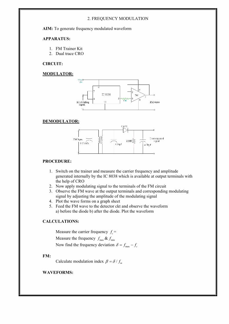
CIRCUIT: MODULATOR:
DEMODULATOR:
PROCEDURE:
1. Switch on the trainer and measure the carrier frequency and amplitude generated internally by the IC 8038 which is available at output terminals with the help of CRO
2. Now apply modulating signal to the terminals of the FM circuit 3. Observe the FM wave at the output terminals and corresponding modulating
signal by adjusting the amplitude of the modulating signal 4. Plot the wave forms on a graph sheet 5. Feed the FM wave to the detector ckt and observe the waveform
a) before the diode b) after the diode. Plot the waveform CALCULATIONS:
Measure the carrier frequency cf =
Measure the frequency maxf & minf
Now find the frequency deviation max cf f
FM:
Calculate modulation index / mf
WAVEFORMS:

RESULT: The modulated wave for the given modulating signal has been verified

VIVA QUESTIONS:
1. What is analog modulation?
2. What is angle modulation?
3. Compare AM with Narrow band FM?
4. What is exponential modulation?
5. What is linear modulation and non-linear modulation?
6. Compare NBFM and WBFM?
7. Advantages and disadvantages of AM and FM?
8. What is Carson rule?
9. What is single tone modulation?
10. Different methods of FM generation and demodulation?
11. What is threshold effect and how to reduce?
12. Relation between FM and PM?
13. What is frequency deviation?

3. RADIO FREQUENCY AMPLIFIER
AIM: To obtain the sensitivity and selectivity characteristics of an RF amplifier. APPARATUS:
4. regulator power supply 5. CRO 6. signal generator
CIRCUIT :
PROCEDURE: a) Sensitivity:
6. Design the RF amplifier to the tuned frequency of 400KHz. 1
2of
LC ,
390 ,C pf L
7. Apply the 100Hz. 50mV signal as an input to the amplifier and note down the output. of 2V p-p.
8. Vary the signal frequency from 100Hz to 1MHz keeping the input voltage constant at 50mV.
9. tabulate the result:
S.NO Frequency Output Gain in dB

10. Note down the frequency at which the output is amx and this maximum voltage value.
11. Draw the frequency response on the semi log. b) Selectivity:
a. Apply 50mV input at the frequency of and note down the output stV .
b. Now vary the frequency in steps of 20 KHz and vary the input voltage to get
the stV in each step.
c. Calculate the attenuation in 20log in
in
V offresonancedB
V atresoance
d. Tabulate the results:
MODEL GRAPH:
RESULT:
S.NO Frequency I/P voltage required to
produce stV attenuation in dB

VIVA QUESTIONS:
1. What is selectivity?
2. What is sensitivity?
3. What is fidelity?
4. What is noise figure?
5. What are the advantages of using RF stage?
6. What is image frequency?
7. Draw backs of TRF receiver?
8. What is double spotting?
9. Why RF amplifier is needed in radio receivers?
10. What are the problems if there no RF amplifier?
11. Compare TRF and SH receivers?
12. Explain the characteristics of radio receivers?
13. RF frequency range?

4. ACTIVE BAND PASS FILTER
AIM: To obtain the frequency response of active Band pass filter whose side band voltage gain is 1 with 3-dB band width of 30 KHz. APPARATUS:
7. CRO 8. Signal generator 9. power supply 10. Resistors: 5.36K, 5.3K, 5.6K 11. Capacitors: 1000pf, 0.1μf
CIRCUIT :
DESIGN EQUATIONS:
Let pfC 10002
Voltage gain = 1
22
22
1
CfR
=5.3K
KHzfHzf 30,300 21
KRR 36.521
fRf
C
1.02
1
11
1
KR 6.53
PROCEDURE:
12. Connect the circuit as shown in the fig. 13. Switch on the power supply and function generator. 14. Apply 20mV signal as an input. 15. Now vary the input frequency, keeping the input voltage constant and at each
step note down the output. 16. tabulate the results:
S.NO Frequency Output voltage Gain in dB

MODEL GRAPH:
RESULT: VIVA QUESTIONS:
1. Explain how to increase the selectivity?
2. Compare the butter worth and chebyshev filter?
3. Derive the expression for transfer function of second order filter?
4. What are the advantages and disadvantages of active filter?
5. Differences between active filters and digital filters?
6. Name various active filters?
7. What is notch filter?
8. What do you know about active filters?
9. Discriminate active and passive filters?
10. What are the characteristics of the filters?

5. ACTIVE LOW PASS FILTER
AIM: To obtain the frequency response of active low pass filter. APPARATUS:
12. CRO 13. Signal generator 14. power supply 15. Resistors: 1.59K, 10K, 5.86K 16. Capacitors: 0.1μf -2Nos
CIRCUIT :
DESIGN EQUATIONS:
2 3 2 3
1
2cf
R R C C
2 3 2 3,let R R R C C C
1 , 0.1 , 1.59ctake f KHz C f R K
1
2cf
RC
1 1
1.586,1 1.586, 0.586f f
Vo
R Rbut again A
R R
1 10.586( 10 )flet R R R K
5.86fR K
PROCEDURE:
17. Apply 100mV, 100Hz signal as an input of this filter and note down the output voltage.
18. Now vary the input frequency, keeping the input voltage constant and at each step note down the output.
19. tabulate the results:
S.NO Frequency Output voltage
Gain in dB

MODEL GRAPH:
RESULT: VIVA QUESTIONS:
1. Explain how to increase the selectivity?
2. Compare the butter worth and chebyshev filter?
3. Derive the expression for transfer function of second order filter?
4. What are the advantages and disadvantages of active filter?
5. Differences between active filters and digital filters?
6. Name various active filters?
7. What is notch filter?
8. What do you know about active filters?
9. Discriminate active and passive filters?

6. ACTIVE HIGH PASS FILTER
AIM: To obtain the frequency response of active High pass filter. APPARATUS:
17. CRO 18. Signal generator 19. power supply 20. Resistors: 33K, 27K, 15.8K 21. Capacitors: 0.0047μf -1Nos
CIRCUIT :
DESIGN EQUATIONS:
2 3 2 3
1
2cf
R R C C
2 3 2 3,let R R R C C C
1 , 0.0047 , 33ctake f KHz C f R K
1
2cf
RC
1
1
1 , 27 , 15.8f
Vo f
Rbut again A R K R k
R
PROCEDURE:
20. Apply 100mV, 100Hz signal as an input of this filter and note down the output voltage.
21. Now vary the input frequency, keeping the input voltage constant and at each step note down the output.
22. tabulate the results:
S.NO Frequency Output voltage
Gain in dB

MODEL GRAPH:
RESULT: VIVA QUESTIONS:
10. Explain how to increase the selectivity?
11. Compare the butter worth and chebyshev filter?
12. Derive the expression for transfer function of second order filter?
13. What are the advantages and disadvantages of active filter?
14. Differences between active filters and digital filters?
15. Name various active filters?
16. What is notch filter?
17. What do you know about active filters?
18. Discriminate active and passive filters?
19. What are the characteristics of the filters?

7. HARMONIC GENERATOR
AIM: To generate different harmonics for a given fundamental frequency of a harmonic generator. APPARATUS:
22. regulator power supply 23. CRO 24. signal generator
CIRCUIT :
PROCEDURE:
23. Connect the circuit as shown in the fig. 24. Switch on the power supply and function generator. 25. Apply 10KHz sinusoidal signal as an input.
26. calculate the theoretical value of inductance using the formula LC
f2
1
27. repeat the process for 1st, 2nd, 3rd hormonics 28. Find the O/P frequency and compare the theoretical frequency with that of
practical frequency. 29. tabulate the results:
RESULT:
S.NO I/P
Frequency Inductance
Output frequency
Theoretical frequency

VIVA QUESTIONS:
1. What is frequency multiplier?
2. Difference between frequency multiplier and frequency mixing?
3. Applications of harmonic generator?
4. Harmonic generator operates in which mode?
5. What is main function of resonance circuit in harmonic generator?

8. PRE-EMPHASIS AND DE-EMPHASIS AIM: To obtain the characteristics of pre-emphasis and de-emphasis. APPARATUS:
1. Regulated power supply 2. CRO 3. Signal Generator 4. transistor SL100 5. resisters 47K, 3.3K, 560Ω, 22K, 10K, 470 Ω, 75K, 1K 6. capacitors 10μf – 2Nos, 33 μf – 1No, 1kpf – 1no
CIRCUIT :
PROCEDURE: Pre-emphasis:
1. Apply input signal, through the signal generator and set the amplitude of
the input signal at 100mv (p-p).
2. Now vary the frequency of the i/p signal from 100Hz to 15 KHz in steps
and note down the output in each case.
3. Tabulate the above readings.
4. Draw the graph frequency Vs gain in db on a semi log sheet.

De-Emphasis:
1. Adopt the same procedure 1 to 4 as above TABULAR FORM:
EXPECTED WAVEFORMS :
RESULT: VIVA QUESTIONS:
1. Draw the circuit of FM transmitter and receiver with pre-emphasis and de-
emphasis network?
2. Draw the pre-emphasis and de-emphasis curves corresponding to different
standards?
3. Compare FM discriminators?
4. What is hard limiter?
5. Define SNR?
6. What is pre-emphasis and de-emphasis?
7. What is threshold effect and how to reduce it?
8. What is FMFB?
S. No I/p signal
frequency (Hz) o/p voltage
Gain in db 20 log V0/Vi

9. PHASE LOCKED LOOP
AIM: To find the lock range by using LM565 APPARATUS:
1. MREC PLL Trainer Kit 2. Decade Resistance Box 3. Signal Generator 4. Multimeter
CIRCUIT: Circuit of PLL:
PIN of IC 565:

PROCEDURE:
1. Connect the circuit as shown in the fig.
2. Check the VCO output at pin 4 of LC 567
3. This is square wave form. The frequency of the wave form is of .
4. Short the IC pins 4 and 5 and give any signal of (1V p-p, 1KHz) and observe
the VCO o/p.
5. When input and output frequencies are equal then note down it as 1f and by
increasing the I/P frequency slowly O/P frequency will also follow the I/P
frequency. This follow up will come up to 2f and going on increasing I/P
frequency, the O/P frequency will back at of only.
6. Now decrease the I/P frequency slowly, at one point I/P and O/P frequencies
will be equal that point of I/P frequency is noted as 2f .
7. by still decreasing I/P frequency, O/P frequency will also follow up once
again, this follow up continuous up to 1f further decreasing I/P frequency,
O/P frequency will once again go back to of only.
THEORETICAL CALCULATIONS:
0 0
1.2
4of
R C , Capture range 1
32
22 3.6 10
c
ff
C
, Lock range 01.39Lf f
0 10 ,f KHz Lock range 2 1Lf f f , Capture range 2 1cf f f
RESULT:

VIVA QUESTIONS:
1. What type of feedback is used in PLL?
2. What is PLL?
3. What are main components in PLL?
4. Define the terms lock range; capture range and free running frequency?
5. What is loop filter?
6. What are main applications of PLL?

10. RADIO FREQUENCY AMPLIFIER
AIM: To obtain the frequency response of an intermediate frequency amplifier. APPARATUS:
25. regulator power supply 26. CRO 27. signal generator 28. transistor SL100 29. resistors 1K, 22K, 1.8K, 400K 30. capacitors 10 µf, 33µf
CIRCUIT:
PROCEDURE:
30. connect the circuit as per the circuit diagram 31. Apply the 1KHz. 50mV signal as an input and note down the output. 32. Vary the signal frequency from upto 1MHz keeping the input voltage constant
at 50mV note down the output. 33. tabulate the result:
34. Draw the frequency response on the semi log.
S.NO Frequency Output Gain in dB

MODEL GRAPH:
RESULT: VIVA QUESTIONS:
1. What are the factors that govern the choice of an amplifier?
2. List out the standard intermediate frequency?
3. What is double conversion? List out the advantages if any?
4. Draw the block diagram of radio receiver. Explain the need of an IF amplifier?
5. What is neutralization?
6. What type of feedback used in IF filter?

11. BALANCED MODULATOR AIM: To study the process of balanced modulation and the corresponding waveform. APPARATUS:
31. balanced modulator Trainer Kit 32. CRO 33. AF generator
CIRCUIT :
Vcc=9V1K 1K
68E
3.9
K
3.9
K0.1uF
10uF
56
E
4.7
K
56
E
4.7K
1K
470uF
10
K
-9V
Modulating
Input
Carrier
Input
Modulated
Output
1
810 3
6
125144
2
MC 1496
BALANCED MODULATOR
PROCEDURE:
6. Switch on the trainer kit and measure the internal carrier frequency and
amplitude by using CRO. It will be around 110 KHz and 200mV record this
frequency as fc.
7. Connect the built in carrier to the carrier input terminal and AF generator
between I/P signal terminal and ground terminals.
8. Observe the I/P and O/P signals simultaneously on CRO
9. Keeping AF signal level to zero and frequency approximately 4KHz. Switch
ON power supply of the board.
10. Slowly increase the AF generator signal level and obtain a stationary balanced
modulated waveform on CRO by adjusting the amplitude of the carrier and the
amplitude and frequency of the modulating signal. Modulated waveform are
not uniform Adjust the pot below the I/P signal terminal.

11. Trace the envelope of modulation waveform from CRO compare this with the
waveform shown in fig.
12. Connect the CRO to the other O/P terminal of balanced modulator and observe
the waveform. Is the two output waveforms are same? Also measure the DC
voltage associated with the O/P.
13. Obtain the trapezoidal pattern on CRO by putting CRO in X-Y mode.
14. Connect both the traces of CRO to both the O/P’s and see the sum and
difference of both the O/P’s.
15. Observe the effect on balanced modulated wave for different settings of AF
signal level, frequency, and comment on the findings.
16. Increase the frequency of the modulating signal to about40KHz and adjust the
sweep so that you get two –three envelops on the CRO screen. Can you
observe the phase reversal in the carrier at the crossing point?
WAVEFORMS :
RESULT:
The frequency doubling and DSB-SC modulation are observed and verified

VIVA QUESTIONS: 1. What is balanced modulator?
2. Draw the spectrum of BM?
3. What is the output of BM?
4. Name different DSB-SC modulators?
5. Compare different AM techniques?
6. What is VSB? And its main application?
7. What is synchronous detector?
8. What is product modulator?
9. What is the use of non linear device?
10. Give mathematical expression for DSB-SC?
11. Which AM technique is preferred over other technique?

12. CONSTANT K-TYPE LOW PASS & HIGH PASS FILTER
AIM: To obtain the characteristics of a K-type low pass and high pass filter. APPARATUS:
34. signal generator 35. CRO 36. Decade inductance box – 3Nos 37. Decade capacitance box – 3Nos 38. Decade resistance box – 1No 39. connecting wires
CIRCUIT: LOW PASS FILTER:
HIGH PASS FILTER:
PROCEDURE: Low pass filter:
35. Design the LPF with a cutoff frequency 4KHz.LC
fc
1 let fC 1.0
mHLmHL 66.312/,4.63
36. Connect the circuit diagram as shown in the circuit diagram 37. Apply the input (50mV, 100Hz signal) and note down the output voltage
reading. 38. Now vary the frequency, keeping the input voltage constant and at each step
note down the output. 39. tabulate the results:

High pass filter:
1. Design the HPF with a cutoff frequency 4KHz.LC
fc4
1
2. Connect the circuit diagram as shown in the circuit diagram 3. Apply the input (50mV, 100Hz signal) and note down the output voltage
reading. 4. Now vary the frequency, keeping the input voltage constant and at each
step note down the output. 5. tabulate the results:
MODEL GRAPH:
LOW PASS FILTER HIGH PASS FILTER
RESULT:
S.NO Frequency Output voltage
Attenuation in dB
S.NO Frequency Output voltage
Attenuation in dB

VIVA QUESTIONS:
1. Give a typical example demonstrating the use of a BPF?
2. What do you know about active filters?
3. Discriminate between active and passive filters?
4. What is filters and classification of filters?
5. What are the characteristics of the filters?
6. What is constant K-type filter? And its draw backs?
7. What is m-derive filter?
8. What are the advantages of m-derive filters over k-type filters?
9. What is the composite filter?
10. What is the lattice filter?
11. What is crystal filter?
12. Explain how m-derive filter is obtained from k-type filter?

13. ACTIVE HIGH PASS FILTER
AIM: To design a asymmetrical and symmetrical π – type attenuator having an attenuation constant at 10dB with a load resistance of 600 Ω. APPARATUS:
40. CRO 41. Signal generator 42. Resistors: 600 Ω, 820 Ω, 1.2K, 1.5K, 1.18KΩ – each 2 Nos
CIRCUIT :
DESIGN EQUATIONS: Symmetrical:
600s LR R
Attenuation constant 1020log 10 , log 3.1620
DD N dB N anti
2( 1) / 2 , ( 1) / 1A L B LR R N N R R N N
Asymmetrical: Attenuation constant: 1020 log 10D N dB
log 3.1620
DN anti
1 2 600s LR R R R , s
L
RS
R

2
2
( 1)1.5
( 2 1)A L
NR R K
N NS
,
21 2 ( 1)
1.22
B
R R NR K
N
,
2
22
11.2
21
B
NR R K
NN
S
PROCEDURE:
40. Connections are made as per the circuit diagram. 41. Input is applied, having amplitude of convenient value with same frequency
the output is measure across the load for this condition. 42. By varying the frequency of input signal maintaining the amplitude of signal
constant and note the output voltage at every step of frequency.
43. The attenuator factor i
o
VN
V is calculated at every stage.
44. Tabulate the results
MODEL GRAPH:
RESULT:
S.NO Frequency Output voltage
i
o
VN
V

VIVA QUESTIONS:
1. What is the need of attenuators?
2. List out the properties of attenuators?
3. How to compare the attenuators?
4. What is an attenuator?
5. Differentiate between symmetric and asymmetric attenuators?
6. What is an equalizer? Describe typical attenuation and phase equalizer?
7. What is image impedance?

14. CONSTANT K-TYPE BAND PASS FILTER
AIM: To obtain the characteristics of a K-type band pass filter. APPARATUS:
43. Decade inductance box – 3Nos 44. Decade capacitance box – 3Nos 45. Decade resistance box – 1No 46. connecting wires
CIRCUIT :
PROCEDURE:
45. design the BPF using the design formula
46. 1 21 2 2 1
1
4 ( )oRL
f f f f
, 2
2 1 oL C R 2 11
2 14 ( )o
f fC
R f f
,
2
2 1
1
( )o
CR f f
47. Connect the circuit diagram as shown in the circuit diagram 48. Apply the input (100mV, 100Hz signal) and note down the output voltage
reading. 49. Now vary the frequency, keeping the input voltage constant and at each step
note down the output. 50. tabulate the results:
MODEL GRAPH:
S.NO Frequency Output voltage
Attenuation in dB

RESULT: VIVA QUESTIONS:
13. Give a typical example demonstrating the use of a BPF?
14. What do you know about active filters?
15. Discriminate between active and passive filters?
16. What is filters and classification of filters?
17. What are the characteristics of the filters?
18. What is constant K-type filter? And its draw backs?
19. What is m-derive filter?
20. What are the advantages of m-derive filters over k-type filters?
21. What is the composite filter?
22. What is the lattice filter?
23. What is crystal filter?
24. Explain how m-derive filter is obtained from k-type filter?