slvsa83 – june 2010 2.95-vto 6-vinput, 3-aoutput, … · tps54319 slvsa83 – june 2010...
TRANSCRIPT

PH
VIN
POWERPAD
BOOT
VSENSE
COMP
TPS54319
EN
RT /CLK
SS/TR
PWRGD
Css
RT R3
C1
CBOOT
CO
LO
R1
R2
CI
VOUT
VIN
AGND
GND
40
50
60
70
80
90
0
10
20
30
100
Eff
icie
nc
y -
%
0 0.5 2 2.5 3
Output Current - A
1 1.5
5 Vin, 1.8 Vout
3.3 Vin,1.8 Vout
TPS54319
www.ti.com SLVSA83 –JUNE 2010
2.95-V to 6-V Input, 3-A Output, 2-MHz, Synchronous Step-DownSwitcher With Integrated FETs ( SWIFT™)
Check for Samples: TPS54319
1FEATURES DESCRIPTION2• Two 45-mΩ (typical) MOSFETs for High The TPS54319 device is a full featured 6 V, 3 A,
Efficiency at 3-A Loads synchronous step down current mode converter withtwo integrated MOSFETs.• 300kHz to 2MHz Switching Frequency
• 0.8 V ± 3.0% Voltage Reference Over The TPS54319 enables small designs by integratingthe MOSFETs, implementing current mode control toTemperature (0°C to 85°C)reduce external component count, reducing inductor• Synchronizes to External Clocksize by enabling up to 2 MHz switching frequency,
• Adjustable Slow Start/Sequencing and minimizing the IC footprint with a small 3mm x• UV and OV Power Good Output 3mm thermally enhanced QFN package.• –40°C to 150°C Operating Junction The TPS54319 provides accurate regulation for a
Temperature Range variety of loads with an accurate ±3.0% VoltageReference (VREF) over temperature.• Thermally Enhanced 3mm × 3mm 16-pin QFN
• Pin Compatible to TPS54318 Efficiency is maximized through the integrated 45mΩMOSFETs and 360mA typical supply current. Usingthe enable pin, shutdown supply current is reduced toAPPLICATIONS2 µA by entering a shutdown mode.• Low-Voltage, High-Density Power Systems
• Point-of-Load Regulation for Consumer Under voltage lockout is internally set at 2.6 V, butApplications such as Set Top Boxes, LCD can be increased by programming the threshold withDisplays, CPE Equipment a resistor network on the enable pin. The output
voltage startup ramp is controlled by the slow startpin. An open drain power good signal indicates theSIMPLIFIED SCHEMATICoutput is within 93% to 107% of its nominal voltage.
vertical spacerFrequency fold back and thermal shutdown protects
vertical spacer the device during an over-current condition.
The TPS54319 is supported in the SwitcherPro™Software Tool at www.ti.com/switcherpro.
For more SWIFTTM documentation, see the TIwebsite at www.ti.com/swift.
1
Please be aware that an important notice concerning availability, standard warranty, and use in critical applications of TexasInstruments semiconductor products and disclaimers thereto appears at the end of this data sheet.
2SWIFT, SwitcherPro are trademarks of Texas Instruments.
PRODUCTION DATA information is current as of publication date. Copyright © 2010, Texas Instruments IncorporatedProducts conform to specifications per the terms of the TexasInstruments standard warranty. Production processing does notnecessarily include testing of all parameters.

TPS54319
SLVSA83 –JUNE 2010 www.ti.com
These devices have limited built-in ESD protection. The leads should be shorted together or the device placed in conductive foamduring storage or handling to prevent electrostatic damage to the MOS gates.
ORDERING INFORMATION (1)
TJ PACKAGE PART NUMBER
–40°C to 150°C 3 × 3 mm QFN TPS54319RTE
(1) For the most current package and ordering information, see the Package Option Addendum at the endof this document, or see the TI website at www.ti.com
ABSOLUTE MAXIMUM RATINGS (1)
VALUE UNIT
MIN MAX
Input voltage VIN –0.3 7
EN –0.3 7
BOOT PH + 7
VSENSE –0.3 3V
COMP –0.3 3
PWRGD –0.3 7
SS/TR –0.3 3
RT/CLK –0.3 6
Output voltage BOOT-PH 7
PH –0.6 7 V
PH 10 ns Transient –2 10
Source current EN 100 µA
RT/CLK 100 µA
Sink current COMP 100 µA
PWRGD 10 mA
SS/TR 100 µA
Electrostatic discharge (HBM) QSS 009-105 (JESD22-A114A) (2) 1 kV
Electrostatic discharge (CDM) QSS 009-147 (JESD22-C101B.01) 500 V
Temperature Tj –40 150 °C
Tstg –65 150 °C
(1) Stresses beyond those listed under absolute maximum ratings may cause permanent damage to the device. These are stress ratingsonly, and functional operation of the device at these or any other conditions beyond those indicated under ELECTRICALSPECIFICATIONS is not implied. Exposure to absolute-maximum-rated conditions for extended periods may affect device reliability.
(2) The human body model is a 100-pF capacitor discharged through a 1.5-kΩ resistor into each pin. The machine model is a 200-pFcapacitor discharged directly into each pin.
2 Submit Documentation Feedback Copyright © 2010, Texas Instruments Incorporated
Product Folder Link(s): TPS54319

TPS54319
www.ti.com SLVSA83 –JUNE 2010
THERMAL INFORMATIONTPS54319
THERMAL METRIC (1) (2) UNITSRTE (16-PINS)
qJA Junction-to-ambient thermal resistance (standard board) 51.7
qJA Junction-to-ambient thermal resistance (custom board) (3) 37.0
yJT Junction-to-top characterization parameter 0.8
yJB Junction-to-board characterization parameter 19.2 °C/W
qJC(top) Junction-to-case(top) thermal resistance 69.3
qJC(bottom) Junction-to-case(bottom) thermal resistance 6.2
qJB Junction-to-board thermal resistance 22
(1) For more information about traditional and new thermal metrics, see the IC Package Thermal Metrics application report, SPRA953.(2) Power rating at a specific ambient temperature TA should be determined with a junction temperature of 150°C. This is the point where
distortion starts to substantially increase. See power dissipation estimate in application section of this data sheet for more information.(3) Test boards conditions:
(a) 2 inches x 2 inches, 4 layers, thickness: 0.062 inch(b) 2 oz. copper traces located on the top of the PCB(c) 2 oz. copper ground planes on the 2 internal layers and bottom layer(d) 4 thermal vias (10mil) located under the device package
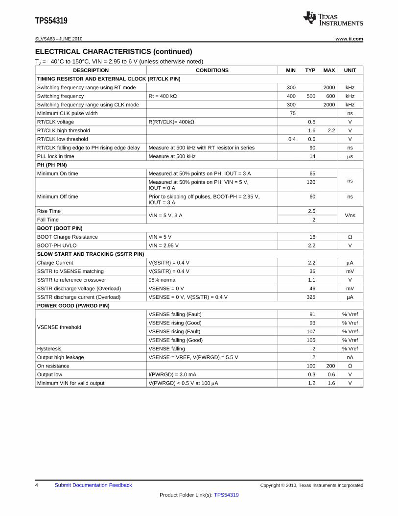
ELECTRICAL CHARACTERISTICSTJ = –40°C to 150°C, VIN = 2.95 to 6 V (unless otherwise noted)
DESCRIPTION CONDITIONS MIN TYP MAX UNIT
SUPPLY VOLTAGE (VIN PIN)
Operating input voltage 2.95 6 V
Internal under voltage lockout threshold 2.6 2.8 V
Shutdown supply current EN = 0 V, 25°C, 2.95 V ≤ VIN ≤ 6 V 2 5 mA
Quiescent Current - Iq VSENSE = 0.9 V, VIN = 5 V, 25°C, RT = 400 kΩ 360 575 mA
ENABLE AND UVLO (EN PIN)
Enable threshold Rising 1.25 V
Falling 1.18
Enable threshold + 50 mV –4.6Input current mA
Enable threshold – 50 mV –1.2
VOLTAGE REFERENCE (VSENSE PIN)
Voltage Reference 2.95 V ≤ VIN ≤ 6 V, 0°C <TJ < 85°C 0.802 0.827 0.852 V
MOSFET
BOOT-PH= 5 V 45 81High side switch resistance mΩ
BOOT-PH= 2.95 V 64 110
VIN= 5 V 42 81Low side switch resistance mΩ
VIN= 2.95 V 59 110
ERROR AMPLIFIER
Input current 7 nA
Error amplifier transconductance (gm) –2 mA < I(COMP) < 2 mA, V(COMP) = 1 V 245 mmhos
Error amplifier transconductance (gm) during –2 mA < I(COMP) < 2 mA, V(COMP) = 1 V, 79 mmhosslow start Vsense = 0.4 V
Error amplifier source/sink V(COMP) = 1 V, 100 mV overdrive +20 mA–20
COMP to Iswitch gm 18 A/V
CURRENT LIMIT
Current limit threshold 3V 4.2 6.6 A
THERMAL SHUTDOWN
Thermal Shutdown 165 °C
Hysteresis 15 °C
Copyright © 2010, Texas Instruments Incorporated Submit Documentation Feedback 3
Product Folder Link(s): TPS54319
TPS54319
SLVSA83 –JUNE 2010 www.ti.com
ELECTRICAL CHARACTERISTICS (continued)TJ = –40°C to 150°C, VIN = 2.95 to 6 V (unless otherwise noted)
DESCRIPTION CONDITIONS MIN TYP MAX UNIT
TIMING RESISTOR AND EXTERNAL CLOCK (RT/CLK PIN)
Switching frequency range using RT mode 300 2000 kHz
Switching frequency Rt = 400 kΩ 400 500 600 kHz
Switching frequency range using CLK mode 300 2000 kHz
Minimum CLK pulse width 75 ns
RT/CLK voltage R(RT/CLK)= 400kΩ 0.5 V
RT/CLK high threshold 1.6 2.2 V
RT/CLK low threshold 0.4 0.6 V
RT/CLK falling edge to PH rising edge delay Measure at 500 kHz with RT resistor in series 90 ns
PLL lock in time Measure at 500 kHz 14 ms
PH (PH PIN)
Minimum On time Measured at 50% points on PH, IOUT = 3 A 65nsMeasured at 50% points on PH, VIN = 5 V, 120
IOUT = 0 A
Minimum Off time Prior to skipping off pulses, BOOT-PH = 2.95 V, 60 nsIOUT = 3 A
Rise Time 2.5VIN = 5 V, 3 A V/ns
Fall Time 2
BOOT (BOOT PIN)
BOOT Charge Resistance VIN = 5 V 16 ΩBOOT-PH UVLO VIN = 2.95 V 2.2 V
SLOW START AND TRACKING (SS/TR PIN)
Charge Current V(SS/TR) = 0.4 V 2.2 mA
SS/TR to VSENSE matching V(SS/TR) = 0.4 V 35 mV
SS/TR to reference crossover 98% normal 1.1 V
SS/TR discharge voltage (Overload) VSENSE = 0 V 46 mV
SS/TR discharge current (Overload) VSENSE = 0 V, V(SS/TR) = 0.4 V 325 µA
POWER GOOD (PWRGD PIN)
VSENSE falling (Fault) 91 % Vref
VSENSE rising (Good) 93 % VrefVSENSE threshold
VSENSE rising (Fault) 107 % Vref
VSENSE falling (Good) 105 % Vref
Hysteresis VSENSE falling 2 % Vref
Output high leakage VSENSE = VREF, V(PWRGD) = 5.5 V 2 nA
On resistance 100 200 ΩOutput low I(PWRGD) = 3.0 mA 0.3 0.6 V
Minimum VIN for valid output V(PWRGD) < 0.5 V at 100 mA 1.2 1.6 V
4 Submit Documentation Feedback Copyright © 2010, Texas Instruments Incorporated
Product Folder Link(s): TPS54319

PW
RG
D
BO
OT
PH
RT
/CLK
EN
AG
ND
VIN
VS
EN
SE
CO
MP
15 14 13
GND
12
11
10
9
8765
16
GND
VIN
VIN
PH
PH1
2
3
4 SS/TR
PowerPAD
(17)
QFN16
RTE PACKAGE
(TOP VIEW)
TPS54319
www.ti.com SLVSA83 –JUNE 2010
DEVICE INFORMATION
PIN CONFIGURATION
PIN FUNCTIONSPIN
DESCRIPTIONNAME NO.
AGND 5 Analog Ground should be electrically connected to GND close to the device.
BOOT 13 A bootstrap capacitor is required between BOOT and PH. If the voltage on this capacitor is below the minimumrequired by the BOOT UVLO, the output is forced to switch off until the capacitor is refreshed.
COMP 7 Error amplifier output, and input to the output switch current comparator. Connect frequency compensationcomponents to this pin.
EN 15 Enable pin, internal pull-up current source. Pull below 1.2 V to disable. Float to enable. Can be used to set theon/off threshold (adjust UVLO) with two additional resistors.
GND 3, 4 Power Ground. This pin should be electrically connected directly to the power pad under the IC.
PH 10, 11, The source of the internal high side power MOSFET, and drain of the internal low side (synchronous) rectifier12 MOSFET.
PowerPAD 17 GND pin should be connected to the exposed power pad for proper operation. This power pad should beconnected to any internal PCB ground plane using multiple vias for good thermal performance.
PWRGD 14 An open drain output; asserts low if output voltage is low due to thermal shutdown, overcurrent,over/under-voltage or EN shut down.
RT/CLK 8 Resistor Timing or External Clock input pin.
SS/TR 9 Slow start and tracking. An external capacitor connected to this pin sets the output voltage rise time.This pin can also be used for tracking.
VIN 1, 2, 16 Input supply voltage, 2.95 V to 6 V.
VSENSE 6 Inverting node of the transconductance (gm) error amplifier.
Copyright © 2010, Texas Instruments Incorporated Submit Documentation Feedback 5
Product Folder Link(s): TPS54319

ERROR
AMPLIFIER
Boot
Charge
Boot
UVLO
UVLO
Current
Sense
Oscillator
with PLL
Frequency
Shift
Slope
Compensation
PWM
Comparator
Minimum
COMP Clamp
Maximum
Clamp
Voltage
Reference
Overload
Recovery
VSENSE
SS/TR
COMP
RT/CLK
PH
BOOT
VIN
AGND
Thermal
Shutdown
EN
Enable
Comparator
Shutdown
Logic
Shutdown
Enable
Threshold
TPS54319RTE Block Diagram
Logic
Shutdown
PWRGD
POWERPAD
GND
Logic
Shutdown
107%
93%
S
Logic and PWM
Latch
i1ihys
RT = 400 k ,
V = 5 V
W
I
-50 -25 0 25 50 75 100 125 150
T - Junction Temperature - °CJ
450
455
460
465
470
475
480
485
490
495
500
f-
Sw
itch
ing
Fre
qu
en
cy -
kH
zs
0.02
0.03
0.04
0.05
0.06
0.07
0.08
RD
SO
N -
Sta
tic D
rain
-So
urce O
n-S
tate
Resis
tan
ce -
W
-50 -25 0 25 50 75 100 125 150
T - Junction Temperature - °CJ
High Side Rdson V = 3.3 VIN
Low Side Rdson V = 3.3 VIN
Low Side Rdson V = 5 VIN
High Side Rdson V = 5 VIN
TPS54319
SLVSA83 –JUNE 2010 www.ti.com
FUNCTIONAL BLOCK DIAGRAM
TYPICAL CHARACTERISTICS CURVESHIGH SIDE AND LOW SIDE Rdson vs TEMPERATURE FREQUENCY vs TEMPERATURE
Figure 1. Figure 2.
6 Submit Documentation Feedback Copyright © 2010, Texas Instruments Incorporated
Product Folder Link(s): TPS54319

0.798
0.808
0.818
0.828
0.838
0.848
V = 3.3 VI
0.858
-50 -25 0 25 50 75 100 125 150
T - Junction Temperature - °CJ
V-
Vo
ltag
e R
efe
ren
ce -
Vre
f
V = 3 VI
V = 5 VI
-50 -25 0 25 50 75 100 125 150
T - Junction Temperature - °CJ
6
6.2
6.4
6.6
6.8
7
7.2
7.4
7.6
7.8
8
Hig
h S
ide S
wit
ch
Cu
rren
t -
A
1000
1100
1200
1300
1400
1500
1600
1700
1800
1900
2000
80 100 120 140 160 180 200
RT - Resistance kW
f-
Sw
itch
ing
Fre
qu
en
cy -
KH
zs
300 400 500 600 700 800 900 1000
RT - Resistance - kW
200
300
400
500
600
700
800
900
1000
f-
Sw
itch
ing
Freq
un
cy -
KH
zs
0
25
50
75
100
0 0.1 0.2 0.3 0.4 0.5 0.6 0.7 0.8
Vsense - V
Vsense Falling
Vsense Rising
No
min
al S
wit
ch
ing
Fre
qu
en
cy -
%
170
190
210
230
250
270
290
310
-50 -25 0 25 50 75 100 125 150
T - Junction Temperature - °CJ
EA
- Tra
nsco
nd
ucta
nce -
A/V
m
V = 3.3 VI
TPS54319
www.ti.com SLVSA83 –JUNE 2010
TYPICAL CHARACTERISTICS CURVES (continued)HIGH SIDE CURRENT LIMIT vs TEMPERATURE VOLTAGE REFERENCE vs TEMPERATURE
Figure 3. Figure 4.
SWITCHING FREQUENCY vs SWITCHING FREQUENCY vsRT RESISTANCE LOW FREQUENCY RANGE RT RESISTANCE HIGH FREQUENCY RANGE
Figure 5. Figure 6.
SWITCHING FREQUENCY vs VSENSE TRANSCONDUCTANCE vs TEMPERATURE
Figure 7. Figure 8.
Copyright © 2010, Texas Instruments Incorporated Submit Documentation Feedback 7
Product Folder Link(s): TPS54319

55
60
65
70
75
80
85
90
95
100
105
V = 3.3 VI
-50 -25 0 25 50 75 100 125 150
T - Junction Temperature - °CJ
EA
- Tra
nsco
nd
ucta
nce -
A/V
m
1.15
1.16
1.17
1.18
1.19
1.2
1.21
1.22
1.23
1.24
1.25
1.26
1.27
1.28
1.29
1.3
V = 3.3 V, risingI
-50 -25 0 25 50 75 100 125 150
T - Junction Temperature - °CJ
V = 3.3 V, fallingI
EN
- T
hre
sh
old
- V
-5.15
-5.05
-4.95
-4.85
-4.75
-4.65
-4.55
-4.45
-4.35
-4.25
V = 5 V,
Ven = Threshold +50 mV
I
-50 -25 0 25 50 75 100 125 150
T - Junction Temperature - °CJ
EN
- P
in C
urren
t -
Am
-1.65
-1.55
-1.45
-1.35
-1.25
-1.15
-1.05
-0.95
-0.85
V = 5 V,
Ven = Threshold -50 mV
I
EN
- P
in C
urren
t -
Am
-50 -25 0 25 50 75 100 125 150
T - Junction Temperature - °CJ
-3
-2.8
-2.6
-2.4
-2.2
-2
-1.8
-1.6
-1.4
-50 -30 -10 10 30 50 70 90 110 130 150
T - Junction Temperature - °CJ
V = 5 VI
Iss/t
r -
Ch
arg
e C
urren
t -
Am
2.2
2.3
2.4
2.5
2.6
2.7
2.8
2.9
3
UVLO Start Switching
UVLO Stop Switching
-50 -25 0 25 50 75 100 125 150
T - Junction Temperature - °CJ
V-
Inp
ut
Vo
ltag
e -
VI
TPS54319
SLVSA83 –JUNE 2010 www.ti.com
TYPICAL CHARACTERISTICS CURVES (continued)TRANSCONDUCTANCE (SLOW START) vs
JUNCTION TEMPERATURE EN PIN VOLTAGE vs TEMPERATURE
Figure 9. Figure 10.
EN PIN CURRENT vs TEMPERATURE EN PIN CURRENT vs TEMPERATURE
Figure 11. Figure 12.
CHARGE CURRENT vs TEMPERATURE INPUT VOLTAGE vs TEMPERATURE
Figure 13. Figure 14.
8 Submit Documentation Feedback Copyright © 2010, Texas Instruments Incorporated
Product Folder Link(s): TPS54319

0
0.5
1
1.5
2
2.5
3
Sh
utd
ow
n S
up
ply
Cu
rren
t -
Am
V = 3.3 VI
-50 -25 0 25 50 75 100 125 150
T - Junction Temperature - °CJ
3 3.5 4 4.5 5 5.5 6
V - Input Voltage - VI
T = 25°CJ
0
0.5
1
1.5
2
2.5
3
Sh
utd
ow
n S
up
ply
Cu
rren
t -
Am
325
335
345
355
365
375
385
395
405
415
425
3 3.5 4 4.5 5 5.5 6
V - Input Voltage - VI
Ivin
- S
up
ply
Cu
rren
t -
Am
T = 25°CJ
300
310
320
330
340
350
360
370
380
390
400
-50 -25 0 25 50 75 100 125 150
T - Junction Temperature - °CJ
Ivin
- S
up
ply
Cu
rren
t -
Am
V = 3.3 VI
90
92
94
96
98
100
102
104
106
108
110Vsense Rising, V = 5 VI
Vsense Rising
Vsense Falling
-50 -25 0 25 50 75 100 125 150
T - Junction Temperature - °CJ
PW
RG
D T
hre
sh
old
- %
Vre
f Vsense Falling
0
20
40
60
80
100
120
140
160
-50 -25 0 25 50 75 100 125 150
T - Junction Temperature - °CJ
V = 3.3 VI
RD
SO
N -
Sta
tic D
rain
-So
urc
e O
n-S
tate
Resis
tan
ce -
W
TPS54319
www.ti.com SLVSA83 –JUNE 2010
TYPICAL CHARACTERISTICS CURVES (continued)SHUTDOWN SUPPLY CURRENT vs TEMPERATURE SHUTDOWN SUPPLY CURRENT vs INPUT VOLTAGE
Figure 15. Figure 16.
VIN SUPPLY CURRENT vs JUNCTION TEMPERATURE VIN SUPPLY CURRENT vs INPUT VOLTAGE
Figure 17. Figure 18.
PWRGD THRESHOLD vs TEMPERATURE PWRGD ON-RESISTANCE vs TEMPERATURE
Figure 19. Figure 20.
Copyright © 2010, Texas Instruments Incorporated Submit Documentation Feedback 9
Product Folder Link(s): TPS54319

0
10
20
30
40
50
60
70V = 5 V,
SS = 0.3 V
I
80
-50 -25 0 25 50 75 100 125 150
T - Junction Temperature - °CJ
SS
/TR
- V
sen
se O
ffset
- m
V
TPS54319
SLVSA83 –JUNE 2010 www.ti.com
TYPICAL CHARACTERISTICS CURVES (continued)SS/TR to VSENSE OFFSET vs TEMPERATURE
Figure 21.
OVERVIEW
The TPS54319 is a 6-V, 3-A, synchronous step-down (buck) converter with two integrated n-channel MOSFETs.To improve performance during line and load transients the device implements a constant frequency, peakcurrent mode control which reduces output capacitance and simplifies external frequency compensation design.The wide switching frequency of 300 kHz to 2000 kHz allows for efficiency and size optimization when selectingthe output filter components. The switching frequency is adjusted using a resistor to ground on the RT/CLK pin.The device has an internal phase lock loop (PLL) on the RT/CLK pin that is used to synchronize the powerswitch turn on to a falling edge of an external system clock.
The TPS54319 has a typical default start up voltage of 2.6 V. The EN pin has an internal pull-up current sourcethat can be used to adjust the input voltage under voltage lockout (UVLO) with two external resistors. In addition,the pull up current provides a default condition when the EN pin is floating for the device to operate. The totaloperating current for the TPS54319 is typically 360 mA when not switching and under no load. When the deviceis disabled, the supply current is less than 5 mA.
The integrated 45 mΩ MOSFETs allow for high efficiency power supply designs with continuous output currentsup to 3 amperes.
The TPS54319 reduces the external component count by integrating the boot recharge diode. The bias voltagefor the integrated high side MOSFET is supplied by a capacitor between the BOOT and PH pins. The bootcapacitor voltage is monitored by an UVLO circuit and turns off the high side MOSFET when the voltage fallsbelow a preset threshold. This BOOT circuit allows the TPS54319 to operate approaching 100%. The outputvoltage can be stepped down to as low as the 0.827 V reference.
The TPS54319 has a power good comparator (PWRGD) with 2% hysteresis.
The TPS54319 minimizes excessive output over-voltage transients by taking advantage of the over-voltagepower good comparator. When the regulated output voltage is greater than 107% of the nominal voltage, theover-voltage comparator is activated, and the high side MOSFET is turned off and masked from turning on untilthe output voltage is lower than 105%.
The SS/TR (slow start/tracking) pin is used to minimize inrush currents or provide power supply sequencingduring power up. A small value capacitor should be coupled to the pin for slow start. The SS/TR pin isdischarged before the output power up to ensure a repeatable restart after an over-temperature fault, UVLO faultor disabled condition.
The use of a frequency fold-back circuit reduces the switching frequency during startup and over current faultconditions to help limit the inductor current.
10 Submit Documentation Feedback Copyright © 2010, Texas Instruments Incorporated
Product Folder Link(s): TPS54319

O
0.827 VR2 = R1
V 0.827 V
æ ö´ ç ÷
-è ø
TPS54319
www.ti.com SLVSA83 –JUNE 2010
DETAILED DESCRIPTION
FIXED FREQUENCY PWM CONTROL
The TPS54319 uses an adjustable fixed frequency, peak current mode control. The output voltage is comparedthrough external resistors on the VSENSE pin to an internal voltage reference by an error amplifier which drivesthe COMP pin. An internal oscillator initiates the turn on of the high side power switch. The error amplifier outputis compared to the high side power switch current. When the power switch current reaches the COMP voltagelevel the high side power switch is turned off and the low side power switch is turned on. The COMP pin voltageincreases and decreases as the output current increases and decreases. The device implements a current limitby clamping the COMP pin voltage to a maximum level and also implements a minimum clamp for improvedtransient response performance.
SLOPE COMPENSATION AND OUTPUT CURRENT
The TPS54319 adds a compensating ramp to the switch current signal. This slope compensation preventssub-harmonic oscillations as duty cycle increases. The available peak inductor current remains constant over thefull duty cycle range.
BOOTSTRAP VOLTAGE (BOOT) AND LOW DROPOUT OPERATION
The TPS54319 has an integrated boot regulator and requires a small ceramic capacitor between the BOOT andPH pin to provide the gate drive voltage for the high side MOSFET. The value of the ceramic capacitor should be0.1 mF. A ceramic capacitor with an X7R or X5R grade dielectric with a voltage rating of 10 V or higher isrecommended because of the stable characteristics over temperature and voltage.
To improve drop out, the TPS54319 is designed to operate at 100% duty cycle as long as the BOOT to PH pinvoltage is greater than 2.2 V. The high side MOSFET is turned off using an UVLO circuit, allowing for the lowside MOSFET to conduct when the voltage from BOOT to PH drops below 2.2 V. Since the supply currentsourced from the BOOT pin is very low, the high side MOSFET can remain on for more switching cycles than arerequired to refresh the capacitor, thus the effective duty cycle of the switching regulator is very high.
ERROR AMPLIFIER
The TPS54319 has a transconductance amplifier. The error amplifier compares the VSENSE voltage to the lowerof the SS/TR pin voltage or the internal 0.827 V voltage reference. The transconductance of the error amplifier is245mA/V during normal operation. When the voltage of VSENSE pin is below 0.827 V and the device isregulating using the SS/TR voltage, the gm is typically greater than 79 mA/V, but less than 245 mA/V. Thefrequency compensation components are placed between the COMP pin and ground.
VOLTAGE REFERENCE
The voltage reference system produces a precise ±3.0% voltage reference over temperature by scaling theoutput of a temperature-stable bandgap circuit. The bandgap and scaling circuits produce 0.827 V at thenon-inverting input of the error amplifier.
ADJUSTING THE OUTPUT VOLTAGE
The output voltage is set with a resistor divider from the output node to the VSENSE pin. It is recommended touse divider resistors with 1% tolerance or better. Start with a 100 kΩ for the R1 resistor and use the Equation 1to calculate R2. To improve efficiency at very light loads consider using larger value resistors. If the values aretoo high the regulator is more susceptible to noise and voltage errors from the VSENSE input current arenoticeable.
vertical spacer
vertical spacer
(1)
Copyright © 2010, Texas Instruments Incorporated Submit Documentation Feedback 11
Product Folder Link(s): TPS54319

VSENSE
VO
+
–
TPS54319
R1
R20.827 V
EN
i1
ihysVIN
+
–
TPS54319
R1
R2
1.2 mA
3.4 mA
( )START STOP
6
0.944 V VR1 =
3.47 10-
´ -W
´
( )6
STOP
1.18 R1R2 =
V 1.18 4.6 10 R1-
×W
- + ´ ×
Tss(mS) Iss( A)Css(nF) =
Vref(V)
´ m
TPS54319
SLVSA83 –JUNE 2010 www.ti.com
Figure 22. Voltage Divider Circuit
ENABLE AND ADJUSTING UNDER-VOLTAGE LOCKOUT
The TPS54319 is disabled when the VIN pin voltage falls below 2.6 V. If an application requires a higherunder-voltage lockout (UVLO), use the EN pin as shown in Figure 23 to adjust the input voltage UVLO by usingtwo external resistors. The EN pin has an internal pull-up current source that provides the default condition of theTPS54319 operating when the EN pin floats. Once the EN pin voltage exceeds 1.25 V, an additional 3.4 mA ofhysteresis is added. When the EN pin is pulled below 1.18 V, the 3.4 mA is removed. This additional currentfacilitates input voltage hysteresis.
Figure 23. Adjustable Under Voltage Lock Out
(2)
vertical spacer
(3)
SLOW START / TRACKING PIN
The TPS54319 regulates to the lower of the SS/TR pin and the internal reference voltage. A capacitor on theSS/TR pin to ground implements a slow start time. The TPS54319 has an internal pull-up current source of2.2mA which charges the external slow start capacitor. Equation 4 calculates the required slow start capacitorvalue where Tss is the desired slow start time in ms, Iss is the internal slow start charging current of 2.2 mA, andVref is the internal voltage reference of 0.827 V.
vertical spacer
(4)
12 Submit Documentation Feedback Copyright © 2010, Texas Instruments Incorporated
Product Folder Link(s): TPS54319

SS2
TPS54319
EN2
PWRGD2
SS1
EN1PWRGD1
Vout2
Vou t1
PWRGD1
EN2
EN1
TPS54319
www.ti.com SLVSA83 –JUNE 2010
If during normal operation, the VIN goes below the UVLO, EN pin pulled below 1.2 V, or a thermal shutdownevent occurs, the TPS54319 stops switching. When the VIN goes above UVLO, EN is released or pulled high, ora thermal shutdown is exited, then SS/TR is discharged to below 40 mV before reinitiating a powering upsequence. The VSENSE voltage will follow the SS/TR pin voltage with a 35mV offset up to 85% of the internalvoltage reference. When the SS/TR voltage is greater than 85% on the internal reference voltage the offsetincreases as the effective system reference transitions from the SS/TR voltage to the internal voltage reference.
SEQUENCING
Many of the common power supply sequencing methods can be implemented using the SS/TR, EN and PWRGDpins. The sequential method can be implemented using an open drain or collector output of a power on reset pinof another device. Figure 24 shows the sequential method. The power good is coupled to the EN pin on theTPS54319 which enables the second power supply once the primary supply reaches regulation.
Ratio-metric start up can be accomplished by connecting the SS/TR pins together. The regulator outputs rampup and reach regulation at the same time. When calculating the slow start time the pull up current source mustbe doubled in Equation 4. The ratio metric method is illustrated in Figure 26.
Figure 24. Sequential Start-Up Sequence Figure 25. Sequential Startup using EN andPWRGD
Copyright © 2010, Texas Instruments Incorporated Submit Documentation Feedback 13
Product Folder Link(s): TPS54319

SS1
Vout2
EN1/2
Vou t1
SS/TR1
TPS54319
EN1
PWRGD1
SS/TR2
TPS54319
EN2
PWRGD2
D´
Vout2 + V VssoffsetR1 =
Vref Iss
´
D -
Vref R1R2 =
Vout2 + V Vref
V = Vout1 Vout2D -
R1 2930 Vout1 145 V> ´ - ´ D
TPS54319
SLVSA83 –JUNE 2010 www.ti.com
Figure 26. Schematic for Ratio-metric Start-Up Figure 27. Ratio-metric Startup with Vout1 LeadingSequence Vout2
vertical spacer
Ratio-metric and simultaneous power supply sequencing can be implemented by connecting the resistor networkof R1 and R2 shown in Figure 28 to the output of the power supply that needs to be tracked or another voltagereference source. Using Equation 5 and Equation 6, the tracking resistors can be calculated to initiate the Vout2slightly before, after or at the same time as Vout1. Equation 7 is the voltage difference between Vout1 andVout2. The ΔV variable is zero volts for simultaneous sequencing. To minimize the effect of the inherent SS/TRto VSENSE offset (Vssoffset) in the slow start circuit and the offset created by the pullup current source (Iss) andtracking resistors, the Vssoffset and Iss are included as variables in the equations. To design a ratio-metric startup in which the Vout2 voltage is slightly greater than the Vout1 voltage when Vout2 reaches regulation, use anegative number in Equation 5 through Equation 7 for ΔV. Equation 7 will result in a positive number forapplications which the Vout2 is slightly lower than Vout1 when Vout2 regulation is achieved. Since the SS/TR pinmust be pulled below 40mV before starting after an EN, UVLO or thermal shutdown fault, careful selection of thetracking resistors is needed to ensure the device will restart after a fault. Make sure the calculated R1 value fromEquation 5 is greater than the value calculated in Equation 8 to ensure the device can recover from a fault. Asthe SS/TR voltage becomes more than 85% of the nominal reference voltage the Vssoffset becomes larger asthe slow start circuits gradually handoff the regulation reference to the internal voltage reference. The SS/TR pinvoltage needs to be greater than 1.1 V for a complete handoff to the internal voltage reference as shown inFigure 27.
vertical spacer
(5)
vertical spacer
(6)
vertical spacer(7)
vertical spacer(8)
vertical spacer
14 Submit Documentation Feedback Copyright © 2010, Texas Instruments Incorporated
Product Folder Link(s): TPS54319

EN1
Vout2
SS2
Vout1
SS/TR1
TPS54319
EN1
PWRGD1
SS/TR2
TPS54319
EN2
PWRGD2
VOUT1
VOUT 2
R1
R2
W1.0793
311890RT (k ) =
Fsw(kHz)
0.9393
133870Fsw(kHz)
RT(k )=
W
TPS54319
www.ti.com SLVSA83 –JUNE 2010
Figure 28. Ratio-metric and Simultaneous Startup Figure 29. Ratio-metric Start-Up using CoupledSequence SS/TR Pins
CONSTANT SWITCHING FREQUENCY and TIMING RESISTOR (RT/CLK Pin)
The switching frequency of the TPS54319 is adjustable over a wide range from 300 kHz to 2000 kHz by placinga maximum of 700 kΩ and minimum of 85 kΩ, respectively, on the RT/CLK pin. An internal amplifier holds thispin at a fixed voltage when using an external resistor to ground to set the switching frequency. The RT/CLK istypically 0.5 V. To determine the timing resistance for a given switching frequency, use the curve in Figure 5 andFigure 6, or Equation 9.
(9)
vertical spacer
(10)
To reduce the solution size one would typically set the switching frequency as high as possible, but tradeoffs ofthe efficiency, maximum input voltage and minimum controllable on time should be considered.
The minimum controllable on time is typically 65 ns at full current load and 120 ns at no load, and limits themaximum operating input voltage or output voltage.
OVERCURRENT PROTECTION
The TPS54319 implements a cycle by cycle current limit. During each switching cycle the high side switchcurrent is compared to the voltage on the COMP pin. When the instantaneous switch current intersects theCOMP voltage, the high side switch is turned off. During overcurrent conditions that pull the output voltage low,the error amplifier responds by driving the COMP pin high, increasing the switch current. The error amplifieroutput is clamped internally. This clamp functions as a switch current limit.
FREQUENCY SHIFT
To operate at high switching frequencies and provide protection during overcurrent conditions, the TPS54319implements a frequency shift. If frequency shift was not implemented, during an overcurrent condition the lowside MOSFET may not be turned off long enough to reduce the current in the inductor, causing a currentrunaway. With frequency shift, during an overcurrent condition the switching frequency is reduced from 100%,then 50%, then 25%, then 12.5% as the voltage decreases from 0.827 to 0 volts on VSENSE pin to allow the lowside MOSFET to be off long enough to decrease the current in the inductor. During start-up, the switchingfrequency increases as the voltage on VSENSE increases from 0 to 0.827 volts. See Figure 7 for details.
Copyright © 2010, Texas Instruments Incorporated Submit Documentation Feedback 15
Product Folder Link(s): TPS54319

TPS54319
Clock
Source
PLL
RT
RT/CLK
SYNC Clock = 2 V / div
PH = 2 V / div
Time = 500 nsec / div
TPS54319
SLVSA83 –JUNE 2010 www.ti.com
REVERSE OVERCURRENT PROTECTION
The TPS54319 implements low side current protection by detecting the voltage across the low side MOSFET.When the converter sinks current through its low side FET, the control circuit turns off the low side MOSFET ifthe reverse current is typically more than 2 A. By implementing this additional protection scheme, the converter isable to protect itself from excessive current during power cycling and start-up into pre-biased outputs.
SYNCHRONIZE USING THE RT/CLK PIN
The RT/CLK pin is used to synchronize the converter to an external system clock. See Figure 30. To implementthe synchronization feature in a system, connect a square wave to the RT/CLK pin with an on time of at least75ns. If the pin is pulled above the PLL upper threshold, a mode change occurs and the pin becomes asynchronization input. The internal amplifier is disabled and the pin is a high impedance clock input to theinternal PLL. If clocking edges stop, the internal amplifier is re-enabled and the mode returns to the frequency setby the resistor. The square wave amplitude at this pin must transition lower than 0.6 V and higher than 1.6 Vtypically. The synchronization frequency range is 300 kHz to 2000 kHz. The rising edge of the PH issynchronized to the falling edge of RT/CLK pin.
Figure 30. Synchronizing to a System Clock Figure 31. Plot of Synchronizing to System Clock
POWER GOOD (PWRGD PIN)
The PWRGD pin output is an open drain MOSFET. The output is pulled low when the VSENSE voltage entersthe fault condition by falling below 91% or rising above 107% of the nominal internal reference voltage. There isa 2% hysteresis on the threshold voltage, so when the VSENSE voltage rises to the good condition above 93%or falls below 105% of the internal voltage reference the PWRGD output MOSFET is turned off. It isrecommended to use a pull-up resistor between the values of 1kΩ and 100kΩ to a voltage source that is 6 V orless. The PWRGD is in a valid state once the VIN input voltage is greater than 1.2 V.
OVERVOLTAGE TRANSIENT PROTECTION
The TPS54319 incorporates an overvoltage transient protection (OVTP) circuit to minimize voltage overshootwhen recovering from output fault conditions or strong unload transients. The OVTP feature minimizes the outputovershoot by implementing a circuit to compare the VSENSE pin voltage to the OVTP threshold which is 107%of the internal voltage reference. If the VSENSE pin voltage is greater than the OVTP threshold, the high sideMOSFET is disabled preventing current from flowing to the output and minimizing output overshoot. When theVSENSE voltage drops lower than the OVTP threshold the high side MOSFET is allowed to turn on the nextclock cycle.
THERMAL SHUTDOWN
The device implements an internal thermal shutdown to protect itself if the junction temperature exceeds 165°C.The thermal shutdown forces the device to stop switching when the junction temperature exceeds the thermaltrip threshold. Once the die temperature decreases below 150°C, the device reinitiates the power up sequenceby discharging the SS pin to below 40 mV. The thermal shutdown hysteresis is 15°C.
16 Submit Documentation Feedback Copyright © 2010, Texas Instruments Incorporated
Product Folder Link(s): TPS54319
VSENSE
COMP
VO
R1
R3
C1C2
R2
CO RO
gm
245 µA/V
0.827 V
Power Stage
18.0 A/V
PH
RESR
COUT
RL
b
a
c
TPS54319
www.ti.com SLVSA83 –JUNE 2010
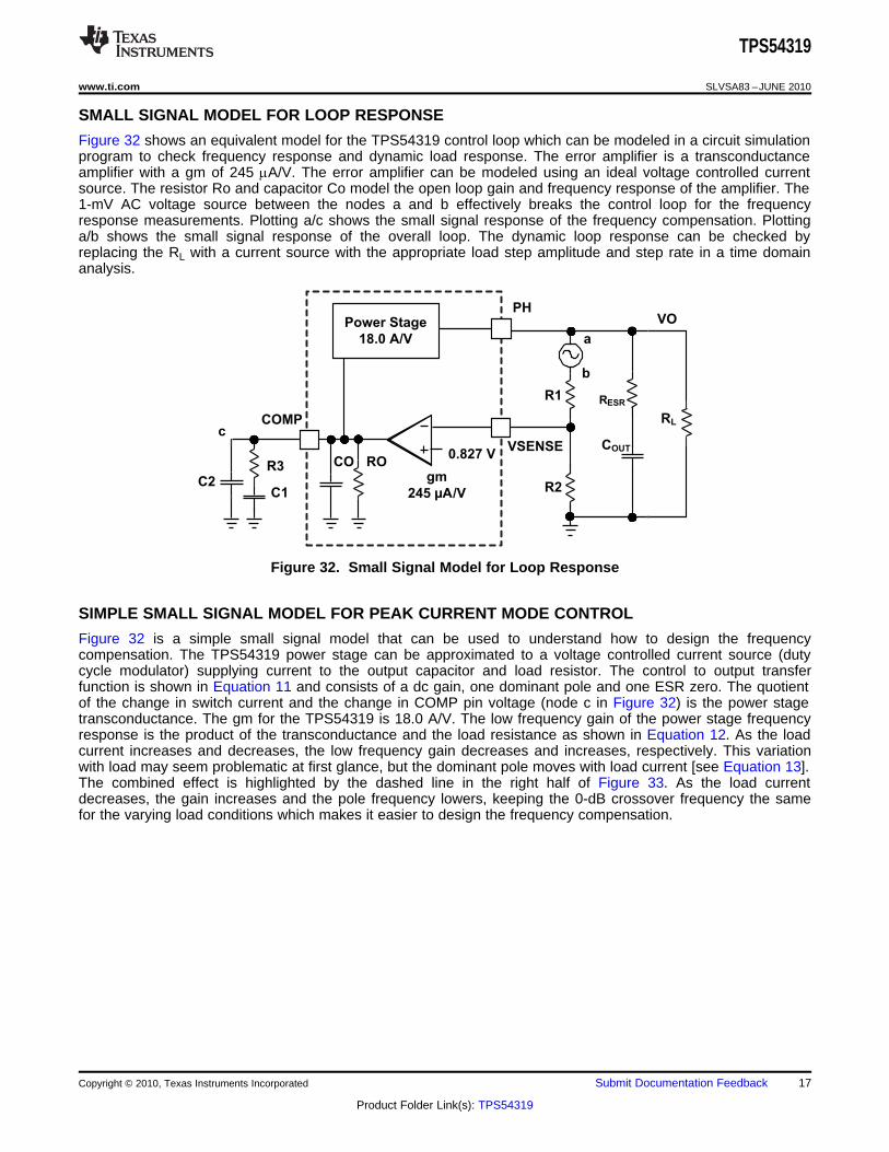
SMALL SIGNAL MODEL FOR LOOP RESPONSE
Figure 32 shows an equivalent model for the TPS54319 control loop which can be modeled in a circuit simulationprogram to check frequency response and dynamic load response. The error amplifier is a transconductanceamplifier with a gm of 245 mA/V. The error amplifier can be modeled using an ideal voltage controlled currentsource. The resistor Ro and capacitor Co model the open loop gain and frequency response of the amplifier. The1-mV AC voltage source between the nodes a and b effectively breaks the control loop for the frequencyresponse measurements. Plotting a/c shows the small signal response of the frequency compensation. Plottinga/b shows the small signal response of the overall loop. The dynamic loop response can be checked byreplacing the RL with a current source with the appropriate load step amplitude and step rate in a time domainanalysis.
Figure 32. Small Signal Model for Loop Response
SIMPLE SMALL SIGNAL MODEL FOR PEAK CURRENT MODE CONTROL
Figure 32 is a simple small signal model that can be used to understand how to design the frequencycompensation. The TPS54319 power stage can be approximated to a voltage controlled current source (dutycycle modulator) supplying current to the output capacitor and load resistor. The control to output transferfunction is shown in Equation 11 and consists of a dc gain, one dominant pole and one ESR zero. The quotientof the change in switch current and the change in COMP pin voltage (node c in Figure 32) is the power stagetransconductance. The gm for the TPS54319 is 18.0 A/V. The low frequency gain of the power stage frequencyresponse is the product of the transconductance and the load resistance as shown in Equation 12. As the loadcurrent increases and decreases, the low frequency gain decreases and increases, respectively. This variationwith load may seem problematic at first glance, but the dominant pole moves with load current [see Equation 13].The combined effect is highlighted by the dashed line in the right half of Figure 33. As the load currentdecreases, the gain increases and the pole frequency lowers, keeping the 0-dB crossover frequency the samefor the varying load conditions which makes it easier to design the frequency compensation.
vertical spacer
vertical spacer
Copyright © 2010, Texas Instruments Incorporated Submit Documentation Feedback 17
Product Folder Link(s): TPS54319

VO
RL
VC
fp
fz
Adc
gmps
RESR
COUT
s1+
2 × zvo= Adc
vc s1+
2 × p
æ ö
ç ÷p ¦è ø
´æ ö
ç ÷p ¦è ø
ps LAdc = gm R´
¦´ ´ pOUT L
1p =
C R 2
¦´ ´ pOUT ESR
1z =
C R 2
Vref
VO
R1
R3
C1
C2R2
CO
5pFRO
gmea
COMP
VSENSE
Type 2A Type 2B
R3
C1
TPS54319
SLVSA83 –JUNE 2010 www.ti.com
Figure 33. Simple Small Signal Model and Frequency Response for Peak Current Mode Control
(11)
(12)
(13)
vertical spacer
(14)
SMALL SIGNAL MODEL FOR FREQUENCY COMPENSATION
The TPS54319 uses a transconductance amplifier for the error amplifier and readily supports two of thecommonly used frequency compensation circuits. The compensation circuits are shown in Figure 34. The Type 2circuits are most likely implemented in high bandwidth power supply designs using low ESR output capacitors. InType 2A, one additional high frequency pole is added to attenuate high frequency noise.
Figure 34. Types of Frequency Compensation
18 Submit Documentation Feedback Copyright © 2010, Texas Instruments Incorporated
Product Folder Link(s): TPS54319
¦p ´ ´
Iout maxp mod =
2 Vout Cout
¦p ´ ´
1z mod =
2 Resr Cout
¦ ¦ ´ ¦C = p mod z mod
¦¦ ¦ ´C
sw= p mod
2
p ¦ ´ ´
´ ´
OUT
ea ps
2 × c Vo CR3 =
gm Vref gm
¦´ ´ pOUT L
1p =
C R 2
´L OUTR CC1 =
R3
´ OUTResr CC2 =
R3
TPS54319
www.ti.com SLVSA83 –JUNE 2010
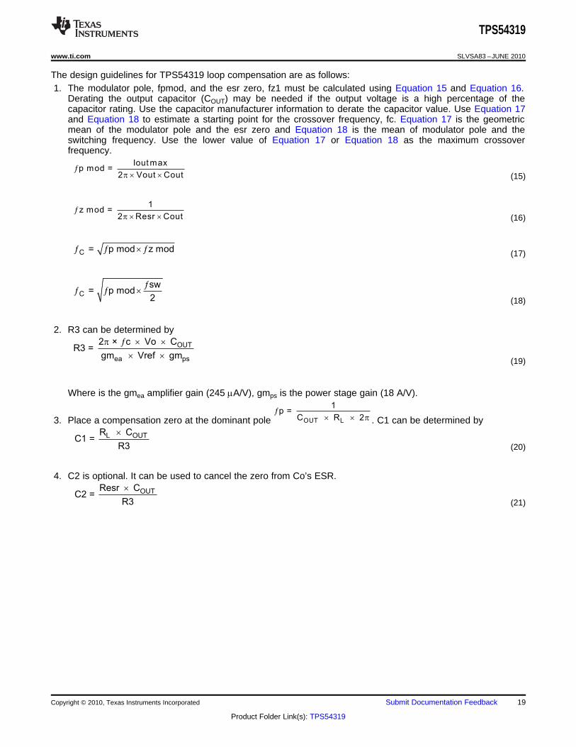
The design guidelines for TPS54319 loop compensation are as follows:1. The modulator pole, fpmod, and the esr zero, fz1 must be calculated using Equation 15 and Equation 16.
Derating the output capacitor (COUT) may be needed if the output voltage is a high percentage of thecapacitor rating. Use the capacitor manufacturer information to derate the capacitor value. Use Equation 17and Equation 18 to estimate a starting point for the crossover frequency, fc. Equation 17 is the geometricmean of the modulator pole and the esr zero and Equation 18 is the mean of modulator pole and theswitching frequency. Use the lower value of Equation 17 or Equation 18 as the maximum crossoverfrequency.
(15)
vertical spacer
(16)
vertical spacer
(17)
vertical spacer
(18)
vertical spacer2. R3 can be determined by
(19)
vertical spacer
Where is the gmea amplifier gain (245 mA/V), gmps is the power stage gain (18 A/V).
3. Place a compensation zero at the dominant pole . C1 can be determined by
(20)
vertical spacer4. C2 is optional. It can be used to cancel the zero from Co’s ESR.
(21)
Copyright © 2010, Texas Instruments Incorporated Submit Documentation Feedback 19
Product Folder Link(s): TPS54319
TPS54319
SLVSA83 –JUNE 2010 www.ti.com
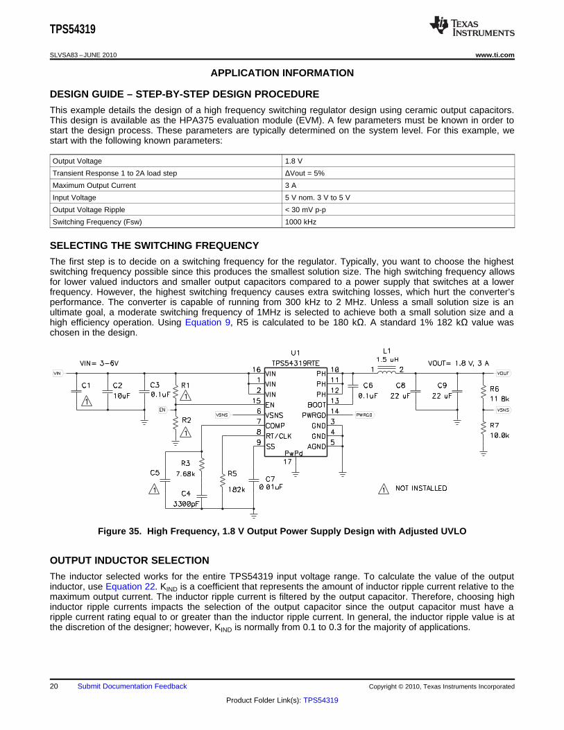
APPLICATION INFORMATION
DESIGN GUIDE – STEP-BY-STEP DESIGN PROCEDURE
This example details the design of a high frequency switching regulator design using ceramic output capacitors.This design is available as the HPA375 evaluation module (EVM). A few parameters must be known in order tostart the design process. These parameters are typically determined on the system level. For this example, westart with the following known parameters:
Output Voltage 1.8 V
Transient Response 1 to 2A load step ΔVout = 5%
Maximum Output Current 3 A
Input Voltage 5 V nom. 3 V to 5 V
Output Voltage Ripple < 30 mV p-p
Switching Frequency (Fsw) 1000 kHz
SELECTING THE SWITCHING FREQUENCY
The first step is to decide on a switching frequency for the regulator. Typically, you want to choose the highestswitching frequency possible since this produces the smallest solution size. The high switching frequency allowsfor lower valued inductors and smaller output capacitors compared to a power supply that switches at a lowerfrequency. However, the highest switching frequency causes extra switching losses, which hurt the converter’sperformance. The converter is capable of running from 300 kHz to 2 MHz. Unless a small solution size is anultimate goal, a moderate switching frequency of 1MHz is selected to achieve both a small solution size and ahigh efficiency operation. Using Equation 9, R5 is calculated to be 180 kΩ. A standard 1% 182 kΩ value waschosen in the design.
Figure 35. High Frequency, 1.8 V Output Power Supply Design with Adjusted UVLO
OUTPUT INDUCTOR SELECTION
The inductor selected works for the entire TPS54319 input voltage range. To calculate the value of the outputinductor, use Equation 22. KIND is a coefficient that represents the amount of inductor ripple current relative to themaximum output current. The inductor ripple current is filtered by the output capacitor. Therefore, choosing highinductor ripple currents impacts the selection of the output capacitor since the output capacitor must have aripple current rating equal to or greater than the inductor ripple current. In general, the inductor ripple value is atthe discretion of the designer; however, KIND is normally from 0.1 to 0.3 for the majority of applications.
20 Submit Documentation Feedback Copyright © 2010, Texas Instruments Incorporated
Product Folder Link(s): TPS54319

-´
´ ´ ¦
Vinmax Vout VoutL1 =
Io Kind Vinmax sw
-´
´ ¦
Vinmax Vout VoutIripple =
L1 Vinmax sw
æ ö´ -´ ç ÷
´ ´ ¦è ø
2
2 1 Vo (Vinmax Vo)ILrms = Io +
12 Vinmax L1 sw
IrippleILpeak = Iout +
2
2 IoutCo >
sw Vout
´ D
¦ ´ D
TPS54319
www.ti.com SLVSA83 –JUNE 2010
For this design example, use KIND = 0.3 and the inductor value is calculated to be 1.36 mH. For this design, anearest standard value was chosen: 1.5 mH. For the output filter inductor, it is important that the RMS currentand saturation current ratings not be exceeded. The RMS and peak inductor current can be found fromEquation 24 and Equation 25.
For this design, the RMS inductor current is 3.01 A and the peak inductor current is 3.72 A. The chosen inductoris a Coilcraft XLA4020-152ME_. It has a saturation current rating 0f 9.6 A and a RMS current rating of 7.5 A.
The current flowing through the inductor is the inductor ripple current plus the output current. During power up,faults or transient load conditions, the inductor current can increase above the calculated peak inductor currentlevel calculated above. In transient conditions, the inductor current can increase up to the switch current limit ofthe device. For this reason, the most conservative approach is to specify an inductor with a saturation currentrating equal to or greater than the switch current limit rather than the peak inductor current.
(22)
vertical spacer
(23)
vertical spacer
(24)
vertical spacer
(25)
OUTPUT CAPACITOR
There are three primary considerations for selecting the value of the output capacitor. The output capacitordetermines the modulator pole, the output voltage ripple, and how the regulator responds to a large change inload current. The output capacitance needs to be selected based on the more stringent of these three criteria.
The desired response to a large change in the load current is the first criteria. The output capacitor needs tosupply the load with current when the regulator can not. This situation would occur if there are desired hold-uptimes for the regulator where the output capacitor must hold the output voltage above a certain level for aspecified amount of time after the input power is removed. The regulator is temporarily not able to supplysufficient output current if there is a large, fast increase in the current needs of the load such as transitioningfrom no load to a full load. The regulator usually needs two or more clock cycles for the control loop to see thechange in load current and output voltage and adjust the duty cycle to react to the change. The output capacitormust be sized to supply the extra current to the load until the control loop responds to the load change. Theoutput capacitance must be large enough to supply the difference in current for 2 clock cycles while only allowinga tolerable amount of droop in the output voltage. Equation 26 shows the minimum output capacitance necessaryto accomplish this.
For this example, the transient load response is specified as a 5 % change in Vout for a load step from 0 A (noload) to 1.5 A (50% load). For this example, ΔIout = 1.5-0 = 1.5 A and ΔVout= 0.05 × 1.8 = 0.090 V. Using thesenumbers gives a minimum capacitance of 33 mF. This value does not take the ESR of the output capacitor intoaccount in the output voltage change. For ceramic capacitors, the ESR is usually small enough to ignore in thiscalculation.
Equation 27 calculates the minimum output capacitance needed to meet the output voltage ripple specification.Where fsw is the switching frequency, Vripple is the maximum allowable output voltage ripple, and Iripple is theinductor ripple current. In this case, the maximum output voltage ripple is 30 mV. Under this requirement,Equation 27 yields 2.3 uF.
vertical spacer
(26)
Copyright © 2010, Texas Instruments Incorporated Submit Documentation Feedback 21
Product Folder Link(s): TPS54319

1 1Co >
Voripple8 sw
Iripple
´´ ¦
VorippleResr <
Iripple
´ -
´ ´ ´ ¦
Vout (Vinmax Vout)Icorms =
12 Vinmax L1 sw
( )Vinmin VoutVoutIcirms = Iout
Vinmin Vinmin
-
´ ´
Ioutmax 0.25Vin =
Cin sw
´D
´ ¦
TPS54319
SLVSA83 –JUNE 2010 www.ti.com
vertical spacer
Where ΔIout is the change in output current, Fsw is the regulators switching frequency and ΔVout is theallowable change in the output voltage. (27)
vertical spacer
Equation 28 calculates the maximum ESR an output capacitor can have to meet the output voltage ripplespecification. Equation 28 indicates the ESR should be less than 55 mΩ. In this case, the ESR of the ceramiccapacitor is much less than 55 mΩ.
Additional capacitance de-ratings for aging, temperature and DC bias should be factored in which increases thisminimum value. For this example, two 22 mF 10 V X5R ceramic capacitors with 3 mΩ of ESR are used.
Capacitors generally have limits to the amount of ripple current they can handle without failing or producingexcess heat. An output capacitor that can support the inductor ripple current must be specified. Some capacitordata sheets specify the RMS (Root Mean Square) value of the maximum ripple current. Equation 29 can be usedto calculate the RMS ripple current the output capacitor needs to support. For this application, Equation 29 yields333 mA.
(28)
vertical spacer
(29)
INPUT CAPACITOR
The TPS54319 requires a high quality ceramic, type X5R or X7R, input decoupling capacitor of at least 4.7 mF ofeffective capacitance and in some applications a bulk capacitance. The effective capacitance includes any DCbias effects. The voltage rating of the input capacitor must be greater than the maximum input voltage. Thecapacitor must also have a ripple current rating greater than the maximum input current ripple of the TPS54319.The input ripple current can be calculated using Equation 30.
The value of a ceramic capacitor varies significantly over temperature and the amount of DC bias applied to thecapacitor. The capacitance variations due to temperature can be minimized by selecting a dielectric material thatis stable over temperature. X5R and X7R ceramic dielectrics are usually selected for power regulator capacitorsbecause they have a high capacitance to volume ratio and are fairly stable over temperature. The outputcapacitor must also be selected with the DC bias taken into account. The capacitance value of a capacitordecreases as the DC bias across a capacitor increases.
For this example design, a ceramic capacitor with at least a 10 V voltage rating is required to support themaximum input voltage. For this example, one 10 mF and one 0.1 mF 10 V capacitors in parallel have beenselected. The input capacitance value determines the input ripple voltage of the regulator. The input voltageripple can be calculated using Equation 31. Using the design example values, Ioutmax=3 A, Cin=10 mF, Fsw=1MHz, yields an input voltage ripple of 76 mV and a rms input ripple current of 1.47 A.
(30)
vertical spacer
(31)
SLOW START CAPACITOR
The slow start capacitor determines the minimum amount of time it takes for the output voltage to reach its
22 Submit Documentation Feedback Copyright © 2010, Texas Instruments Incorporated
Product Folder Link(s): TPS54319

Tss(ms) Iss( A)Css(nF) =
Vref(V)
´ m
-
VrefR7 = R6
Vo Vref
( ) ( )Voutmin Ontimemin Fsmax Vinmax Ioutmin 2 RDS Ioutmin RL RDS= ´ ´ - ´ ´ - ´ +
( ) ( ) ( )Voutmax 1 Offtimemax Fsmax Vinmin Ioutmax 2 RDS Ioutmax RL RDS= - ´ ´ - ´ ´ - ´ +
TPS54319
www.ti.com SLVSA83 –JUNE 2010
nominal programmed value during power up. This is useful if a load requires a controlled voltage slew rate. Thisis also used if the output capacitance is very large and would require large amounts of current to quickly chargethe capacitor to the output voltage level. The large currents necessary to charge the capacitor may make theTPS54319 reach the current limit or excessive current draw from the input power supply may cause the inputvoltage rail to sag. Limiting the output voltage slew rate solves both of these problems.
The slow start capacitor value can be calculated using Equation 32. For the example circuit, the slow start time isnot too critical since the output capacitor value is 44 mF which does not require much current to charge to 1.8 V.The example circuit has the slow start time set to an arbitrary value of 4ms which requires a 10 nF capacitor. InTPS54319, Iss is 2.2 mA and Vref is 0.827 V.
(32)
BOOTSTRAP CAPACITOR SELECTION
A 0.1 mF ceramic capacitor must be connected between the BOOT to PH pin for proper operation. It isrecommended to use a ceramic capacitor with X5R or better grade dielectric. The capacitor should have 10 V orhigher voltage rating.
OUTPUT VOLTAGE AND FEEDBACK RESISTORS SELECTION
For the example design, 100 kΩ was selected for R6. Using Equation 33, R7 is calculated as 80 kΩ. The neareststandard 1% resistor is 80.5 kΩ.
(33)
Due to the internal design of the TPS54319, there is a minimum output voltage limit for any given input voltage.The output voltage can never be lower than the internal voltage reference of 0.827 V. Above 0.827 V, the outputvoltage may be limited by the minimum controllable on time. The minimum output voltage in this case is given byEquation 34
Where:
Voutmin = minimum achievable output voltage
Ontimemin = minimum controllable on-time (65 ns typical. 120 nsec no load)
Fsmax = maximum switching frequency including tolerance
Vinmax = maximum input voltage
Ioutmin = minimum load current
RDS = minimum high side MOSFET on resistance (45 - 64 mΩ)
RL = series resistance of output inductor (34)
There is also a maximum achievable output voltage which is limited by the minimum off time. The maximumoutput voltage is given by Equation 35
Where:
Voutmax = maximum achievable output voltage
Offtimeman = maximum off time (60 nsec typical)
Fsmax = maximum switching frequency including tolerance
Vinmin = minimum input voltage
Ioutmax = maximum load current
RDS = maximum high side MOSFET on resistance (81 - 110 mΩ)
RL = series resistance of output inductor (35)
Copyright © 2010, Texas Instruments Incorporated Submit Documentation Feedback 23
Product Folder Link(s): TPS54319

¦p ´ ´
Iout maxp mod =
2 Vout Cout
¦p ´ ´
1z mod =
2 Resr Cout
¦ ¦ ´ ¦C = p mod z mod
¦¦ ¦ ´C
sw= p mod
2
gm
2 × c Vo CoR3 =
Gm Vref VI
p ¦ ´ ´
´ ´
´Ro CoC3 =
R3
TPS54319
SLVSA83 –JUNE 2010 www.ti.com
COMPENSATION
There are several industry techniques used to compensate DC/DC regulators. The method presented here iseasy to calculate and yields high phase margins. For most conditions, the regulator has a phase margin between60 and 90 degrees. The method presented here ignores the effects of the slope compensation that is internal tothe TPS54319. Since the slope compensation is ignored, the actual cross over frequency is usually lower thanthe cross over frequency used in the calculations. Use SwitcherPro software for a more accurate design.
To get started, the modulator pole, fpmod, and the esr zero, fz1 must be calculated using Equation 36 andEquation 37. For Cout, derating the capacitor is not needed as the 1.8 V output is a small percentage of the 10 Vcapacitor rating. If the output is a high percentage of the capacitor rating, use the capacitor manufacturerinformation to derate the capacitor value. Use Equation 38 and Equation 39 to estimate a starting point for thecrossover frequency, fc. For the example design, fpmod is 6.03 kHz and fzmod is 1210 kHz. Equation 38 is thegeometric mean of the modulator pole and the esr zero and Equation 39 is the mean of modulator pole and theswitching frequency. Equation 38 yields 85.3 kHz and Equation 39 gives 54.9 kHz. Use the lower value ofEquation 38 or Equation 39 as the approximate crossover frequency. For this example, fc is 56 kHz. Next, thecompensation components are calculated. A resistor in series with a capacitor is used to create a compensatingzero. A capacitor in parallel to these two components forms the compensating pole (if needed).
(36)
vertical spacer
(37)
vertical spacer
(38)
vertical spacer
(39)
vertical spacer
The compensation design takes the following steps:1. Set up the anticipated cross-over frequency. Use Equation 40 to calculate the compensation network’s
resistor value. In this example, the anticipated cross-over frequency (fc) is 56 kHz. The power stage gain(gmps) is 18 A/V and the error amplifier gain (gmea) is 245 mA/V.
(40)
2. Place compensation zero at the pole formed by the load resistor and the output capacitor. The compensationnetwork’s capacitor can be calculated from Equation 41.
(41)
3. An additional pole can be added to attenuate high frequency noise. In this application, it is not necessary toadd it.
From the procedures above, the compensation network includes a 7.68 kΩ resistor and a 3300 pF capacitor.
24 Submit Documentation Feedback Copyright © 2010, Texas Instruments Incorporated
Product Folder Link(s): TPS54319

3.3 Vin,1.8 Vout 5 Vin, 1.8 Vout
0.001 0.01 0.1 1 10
Output Current - A
0
10
20
30
40
50
60
70
80
90
100
Eff
icie
ncy -
%
40
50
60
70
80
90
0
10
20
30
100
Eff
icie
ncy -
%
0 0.5 2 2.5 3
Output Current - A
1 1.5
5 Vin, 1.8 Vout
3.3 Vin,1.8 Vout
1.05 V 1.2 V1.5 V
1.8 V 2.5 V
50
55
60
65
70
75
80
85
90
95
100
Eff
icie
nce -
%
0 0.5 1 1.5 2 2.5 3I - Output Current - AO
50
55
60
65
70
75
80
85
90
95
100
0 0.5 1 1.5 2 2.5 3I - Output Current - AO
1.05V1.2 V
1.5 V1.8 V2.5 V
3.3 V
Eff
icie
nce -
%
Vin = 5 V / div
Vout = 2 V / div
EN = 2 V / div
PWRGD = 5 V / div
Time = 5 msec / div
Vout = 100 mV / div (ac coupled)
Iout = 1 A / div (0 A to 1.5 A load step)
Time = 200 usec / div
TPS54319
www.ti.com SLVSA83 –JUNE 2010
APPLICATION CURVESEFFICIENCY EFFICIENCY
vs vsLOAD CURRENT LOAD CURRENT
Figure 36. Figure 37.
EFFICIENCY EFFICIENCYvs vs
LOAD CURRENT LOAD CURRENT1 MHz, 3.3 VIN, TA = 25°C 1 MHz, 5 VIN, TA = 25°C
Figure 38. Figure 39.
TRANSIENT RESPONSE, 1.5 A STEP POWER UP VOUT, VIN
Figure 40. Figure 41.
Copyright © 2010, Texas Instruments Incorporated Submit Documentation Feedback 25
Product Folder Link(s): TPS54319

Vin = 5 V / div
Vout = 2 V / div
EN = 2 V / div
PWRGD = 5 V / div
Time = 5 msec / div
Vout = 20 mV / div (ac coupled)
PH = 2 V / div
Time = 500 nsec / div
Vin = 100 mV / div (ac coupled)
PH = 2 V / div
Time = 500 nsec / div10 100 1000 10k 100k 1M
Frequency - Hz
–60
Gain
-d
B
50
40
30
20
10
0
–10
–20
–30
–40
–50
60
Ph
ase
-D
eg
rees
150
120
90
60
30
0
–30
–60
–90
–120
–150
–180
180
PhaseGain
3 3.5 5 6
Input Voltage-V
Iout = 2 A
-0.4
-0.3
-0.2
-0.1
0
0.1
0.2
0.3
0.4
Ou
tpu
t V
olt
ag
e D
evia
tio
n -
%
4.5 5.54
Vin = 3.3 V
-0.4
-0.3
-0.2
-0.1
0
0.1
0.2
0.3
0.4
Ou
tpu
t V
olt
ag
e D
evia
tio
n -
%
0 0.5 2 2.5 3
Output Current - A
1 1.5
Vin = 5 V
TPS54319
SLVSA83 –JUNE 2010 www.ti.com
POWER UP VOUT, EN OUTPUT RIPPLE, 3 A
Figure 42. Figure 43.
INPUT RIPPLE, 3 A CLOSED LOOP RESPONSE, VIN (5 V), 3 A
Figure 44. Figure 45.
LOAD REGULATION REGULATIONvs vs
LOAD CURRENT INPUT VOLTAGE
Figure 46. Figure 47.
26 Submit Documentation Feedback Copyright © 2010, Texas Instruments Incorporated
Product Folder Link(s): TPS54319
TPS54319
www.ti.com SLVSA83 –JUNE 2010
POWER DISSIPATION ESTIMATE
The following formulas show how to estimate the IC power dissipation under continuous conduction mode (CCM)operation. The power dissipation of the IC (Ptot) includes conduction loss (Pcon), dead time loss (Pd), switchingloss (Psw), gate drive loss (Pgd) and supply current loss (Pq).
Pcon = Io2 × RDS_on_Temp
Pd = ƒsw × Io × 0.7 × 40 × 10–9
Psw = 1/2 × Vin × Io × ƒsw× 8 × 10⁻⁹
Pgd = 2 × Vin × ƒsw× 2 × 10⁻⁹
Pq = Vin × 360 × 10–6
Where:IO is the output current (A).RDS_on_Temp is the on-resistance of the high-side MOSFET with given temperature (Ω).Vin is the input voltage (V).ƒsw is the switching frequency (Hz).
So
Ptot = Pcon + Pd + Psw + Pgd + Pq
For given TA,
TJ = TA + Rth × Ptot
For given TJMAX = 150°C
TAmax = TJ max – Rth × Ptot
Where:Ptot is the total device power dissipation (W).TA is the ambient temperature (°C).TJ is the junction temperature (°C).Rth is the thermal resistance of the package (°C/W).TJMAX is maximum junction temperature (°C).TAMAX is maximum ambient temperature (°C).
There are additional power losses in the regulator circuit due to the inductor AC and DC losses and traceresistance that impact the overall efficiency of the regulator.
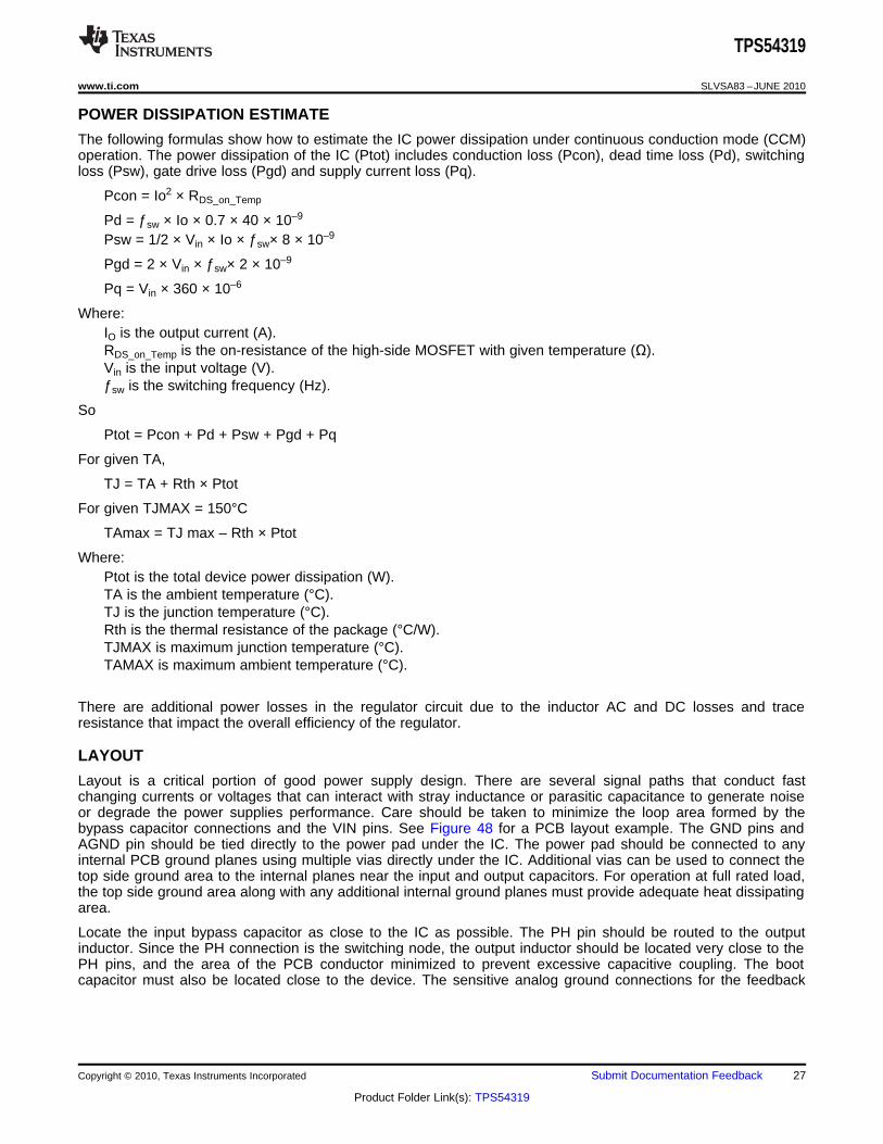
LAYOUT
Layout is a critical portion of good power supply design. There are several signal paths that conduct fastchanging currents or voltages that can interact with stray inductance or parasitic capacitance to generate noiseor degrade the power supplies performance. Care should be taken to minimize the loop area formed by thebypass capacitor connections and the VIN pins. See Figure 48 for a PCB layout example. The GND pins andAGND pin should be tied directly to the power pad under the IC. The power pad should be connected to anyinternal PCB ground planes using multiple vias directly under the IC. Additional vias can be used to connect thetop side ground area to the internal planes near the input and output capacitors. For operation at full rated load,the top side ground area along with any additional internal ground planes must provide adequate heat dissipatingarea.
Locate the input bypass capacitor as close to the IC as possible. The PH pin should be routed to the outputinductor. Since the PH connection is the switching node, the output inductor should be located very close to thePH pins, and the area of the PCB conductor minimized to prevent excessive capacitive coupling. The bootcapacitor must also be located close to the device. The sensitive analog ground connections for the feedback
Copyright © 2010, Texas Instruments Incorporated Submit Documentation Feedback 27
Product Folder Link(s): TPS54319

VIN
VIN
VIN
GND
EN
GND
VS
EN
SE
SS
PH
PH
PH
PW
RG
D
BO
OT
RT
/CLK
CO
MP
AG
ND
PH
BOOT
CAPACITOR
VOUTOUTPUT
INDUCTOR
OUTPUT
FILTER
CAPACITOR
SLOW START
CAPACITOR
COMPENSATION
NETWORK
TOPSIDE
GROUND
AREA
VIA to Ground Plane
FREQUENCY
SET
RESISTOR
ANALOG
GROUND
TRACE
VIN
INPUT
BYPASS
CAPACITOR
VIN
UVLO SET
RESISTORS
FEEDBACK
RESISTORS
VIA to
Ground
Plane
EXPOSED
POWERPAD
AREA
TPS54319
SLVSA83 –JUNE 2010 www.ti.com
voltage divider, compensation components, slow start capacitor and frequency set resistor should be connectedto a separate analog ground trace as shown. The RT/CLK pin is particularly sensitive to noise so the RT resistorshould be located as close as possible to the IC and routed with minimal lengths of trace. The additional externalcomponents can be placed approximately as shown. It may be possible to obtain acceptable performance withalternate PCB layouts, however this layout has been shown to produce good results and is meant as a guideline.
Figure 48. PCB Layout Example
28 Submit Documentation Feedback Copyright © 2010, Texas Instruments Incorporated
Product Folder Link(s): TPS54319

PACKAGE OPTION ADDENDUM
www.ti.com 23-Feb-2014
Addendum-Page 1
PACKAGING INFORMATION
Orderable Device Status(1)
Package Type PackageDrawing
Pins PackageQty
Eco Plan(2)
Lead/Ball Finish(6)
MSL Peak Temp(3)
Op Temp (°C) Device Marking(4/5)
Samples
TPS54319RTER ACTIVE WQFN RTE 16 3000 Green (RoHS& no Sb/Br)
CU NIPDAU Level-2-260C-1 YEAR -40 to 150 54319
TPS54319RTET ACTIVE WQFN RTE 16 250 Green (RoHS& no Sb/Br)
CU NIPDAU Level-2-260C-1 YEAR -40 to 150 54319
(1) The marketing status values are defined as follows:ACTIVE: Product device recommended for new designs.LIFEBUY: TI has announced that the device will be discontinued, and a lifetime-buy period is in effect.NRND: Not recommended for new designs. Device is in production to support existing customers, but TI does not recommend using this part in a new design.PREVIEW: Device has been announced but is not in production. Samples may or may not be available.OBSOLETE: TI has discontinued the production of the device.
(2) Eco Plan - The planned eco-friendly classification: Pb-Free (RoHS), Pb-Free (RoHS Exempt), or Green (RoHS & no Sb/Br) - please check http://www.ti.com/productcontent for the latest availabilityinformation and additional product content details.TBD: The Pb-Free/Green conversion plan has not been defined.Pb-Free (RoHS): TI's terms "Lead-Free" or "Pb-Free" mean semiconductor products that are compatible with the current RoHS requirements for all 6 substances, including the requirement thatlead not exceed 0.1% by weight in homogeneous materials. Where designed to be soldered at high temperatures, TI Pb-Free products are suitable for use in specified lead-free processes.Pb-Free (RoHS Exempt): This component has a RoHS exemption for either 1) lead-based flip-chip solder bumps used between the die and package, or 2) lead-based die adhesive used betweenthe die and leadframe. The component is otherwise considered Pb-Free (RoHS compatible) as defined above.Green (RoHS & no Sb/Br): TI defines "Green" to mean Pb-Free (RoHS compatible), and free of Bromine (Br) and Antimony (Sb) based flame retardants (Br or Sb do not exceed 0.1% by weightin homogeneous material)
(3) MSL, Peak Temp. - The Moisture Sensitivity Level rating according to the JEDEC industry standard classifications, and peak solder temperature.
(4) There may be additional marking, which relates to the logo, the lot trace code information, or the environmental category on the device.
(5) Multiple Device Markings will be inside parentheses. Only one Device Marking contained in parentheses and separated by a "~" will appear on a device. If a line is indented then it is a continuationof the previous line and the two combined represent the entire Device Marking for that device.
(6) Lead/Ball Finish - Orderable Devices may have multiple material finish options. Finish options are separated by a vertical ruled line. Lead/Ball Finish values may wrap to two lines if the finishvalue exceeds the maximum column width.
Important Information and Disclaimer:The information provided on this page represents TI's knowledge and belief as of the date that it is provided. TI bases its knowledge and belief on informationprovided by third parties, and makes no representation or warranty as to the accuracy of such information. Efforts are underway to better integrate information from third parties. TI has taken andcontinues to take reasonable steps to provide representative and accurate information but may not have conducted destructive testing or chemical analysis on incoming materials and chemicals.TI and TI suppliers consider certain information to be proprietary, and thus CAS numbers and other limited information may not be available for release.

PACKAGE OPTION ADDENDUM
www.ti.com 23-Feb-2014
Addendum-Page 2
In no event shall TI's liability arising out of such information exceed the total purchase price of the TI part(s) at issue in this document sold by TI to Customer on an annual basis.

TAPE AND REEL INFORMATION
*All dimensions are nominal
Device PackageType
PackageDrawing
Pins SPQ ReelDiameter
(mm)
ReelWidth
W1 (mm)
A0(mm)
B0(mm)
K0(mm)
P1(mm)
W(mm)
Pin1Quadrant
TPS54319RTER WQFN RTE 16 3000 330.0 12.4 3.3 3.3 1.1 8.0 12.0 Q2
TPS54319RTER WQFN RTE 16 3000 330.0 12.4 3.3 3.3 1.1 8.0 12.0 Q2
TPS54319RTET WQFN RTE 16 250 180.0 12.5 3.3 3.3 1.1 8.0 12.0 Q2
TPS54319RTET WQFN RTE 16 250 180.0 12.4 3.3 3.3 1.1 8.0 12.0 Q2
PACKAGE MATERIALS INFORMATION
www.ti.com 3-Nov-2017
Pack Materials-Page 1

*All dimensions are nominal
Device Package Type Package Drawing Pins SPQ Length (mm) Width (mm) Height (mm)
TPS54319RTER WQFN RTE 16 3000 367.0 367.0 35.0
TPS54319RTER WQFN RTE 16 3000 338.0 355.0 50.0
TPS54319RTET WQFN RTE 16 250 338.0 355.0 50.0
TPS54319RTET WQFN RTE 16 250 210.0 185.0 35.0
PACKAGE MATERIALS INFORMATION
www.ti.com 3-Nov-2017
Pack Materials-Page 2


IMPORTANT NOTICE
Texas Instruments Incorporated (TI) reserves the right to make corrections, enhancements, improvements and other changes to itssemiconductor products and services per JESD46, latest issue, and to discontinue any product or service per JESD48, latest issue. Buyersshould obtain the latest relevant information before placing orders and should verify that such information is current and complete.TI’s published terms of sale for semiconductor products (http://www.ti.com/sc/docs/stdterms.htm) apply to the sale of packaged integratedcircuit products that TI has qualified and released to market. Additional terms may apply to the use or sale of other types of TI products andservices.Reproduction of significant portions of TI information in TI data sheets is permissible only if reproduction is without alteration and isaccompanied by all associated warranties, conditions, limitations, and notices. TI is not responsible or liable for such reproduceddocumentation. Information of third parties may be subject to additional restrictions. Resale of TI products or services with statementsdifferent from or beyond the parameters stated by TI for that product or service voids all express and any implied warranties for theassociated TI product or service and is an unfair and deceptive business practice. TI is not responsible or liable for any such statements.Buyers and others who are developing systems that incorporate TI products (collectively, “Designers”) understand and agree that Designersremain responsible for using their independent analysis, evaluation and judgment in designing their applications and that Designers havefull and exclusive responsibility to assure the safety of Designers' applications and compliance of their applications (and of all TI productsused in or for Designers’ applications) with all applicable regulations, laws and other applicable requirements. Designer represents that, withrespect to their applications, Designer has all the necessary expertise to create and implement safeguards that (1) anticipate dangerousconsequences of failures, (2) monitor failures and their consequences, and (3) lessen the likelihood of failures that might cause harm andtake appropriate actions. Designer agrees that prior to using or distributing any applications that include TI products, Designer willthoroughly test such applications and the functionality of such TI products as used in such applications.TI’s provision of technical, application or other design advice, quality characterization, reliability data or other services or information,including, but not limited to, reference designs and materials relating to evaluation modules, (collectively, “TI Resources”) are intended toassist designers who are developing applications that incorporate TI products; by downloading, accessing or using TI Resources in anyway, Designer (individually or, if Designer is acting on behalf of a company, Designer’s company) agrees to use any particular TI Resourcesolely for this purpose and subject to the terms of this Notice.TI’s provision of TI Resources does not expand or otherwise alter TI’s applicable published warranties or warranty disclaimers for TIproducts, and no additional obligations or liabilities arise from TI providing such TI Resources. TI reserves the right to make corrections,enhancements, improvements and other changes to its TI Resources. TI has not conducted any testing other than that specificallydescribed in the published documentation for a particular TI Resource.Designer is authorized to use, copy and modify any individual TI Resource only in connection with the development of applications thatinclude the TI product(s) identified in such TI Resource. NO OTHER LICENSE, EXPRESS OR IMPLIED, BY ESTOPPEL OR OTHERWISETO ANY OTHER TI INTELLECTUAL PROPERTY RIGHT, AND NO LICENSE TO ANY TECHNOLOGY OR INTELLECTUAL PROPERTYRIGHT OF TI OR ANY THIRD PARTY IS GRANTED HEREIN, including but not limited to any patent right, copyright, mask work right, orother intellectual property right relating to any combination, machine, or process in which TI products or services are used. Informationregarding or referencing third-party products or services does not constitute a license to use such products or services, or a warranty orendorsement thereof. Use of TI Resources may require a license from a third party under the patents or other intellectual property of thethird party, or a license from TI under the patents or other intellectual property of TI.TI RESOURCES ARE PROVIDED “AS IS” AND WITH ALL FAULTS. TI DISCLAIMS ALL OTHER WARRANTIES ORREPRESENTATIONS, EXPRESS OR IMPLIED, REGARDING RESOURCES OR USE THEREOF, INCLUDING BUT NOT LIMITED TOACCURACY OR COMPLETENESS, TITLE, ANY EPIDEMIC FAILURE WARRANTY AND ANY IMPLIED WARRANTIES OFMERCHANTABILITY, FITNESS FOR A PARTICULAR PURPOSE, AND NON-INFRINGEMENT OF ANY THIRD PARTY INTELLECTUALPROPERTY RIGHTS. TI SHALL NOT BE LIABLE FOR AND SHALL NOT DEFEND OR INDEMNIFY DESIGNER AGAINST ANY CLAIM,INCLUDING BUT NOT LIMITED TO ANY INFRINGEMENT CLAIM THAT RELATES TO OR IS BASED ON ANY COMBINATION OFPRODUCTS EVEN IF DESCRIBED IN TI RESOURCES OR OTHERWISE. IN NO EVENT SHALL TI BE LIABLE FOR ANY ACTUAL,DIRECT, SPECIAL, COLLATERAL, INDIRECT, PUNITIVE, INCIDENTAL, CONSEQUENTIAL OR EXEMPLARY DAMAGES INCONNECTION WITH OR ARISING OUT OF TI RESOURCES OR USE THEREOF, AND REGARDLESS OF WHETHER TI HAS BEENADVISED OF THE POSSIBILITY OF SUCH DAMAGES.Unless TI has explicitly designated an individual product as meeting the requirements of a particular industry standard (e.g., ISO/TS 16949and ISO 26262), TI is not responsible for any failure to meet such industry standard requirements.Where TI specifically promotes products as facilitating functional safety or as compliant with industry functional safety standards, suchproducts are intended to help enable customers to design and create their own applications that meet applicable functional safety standardsand requirements. Using products in an application does not by itself establish any safety features in the application. Designers mustensure compliance with safety-related requirements and standards applicable to their applications. Designer may not use any TI products inlife-critical medical equipment unless authorized officers of the parties have executed a special contract specifically governing such use.Life-critical medical equipment is medical equipment where failure of such equipment would cause serious bodily injury or death (e.g., lifesupport, pacemakers, defibrillators, heart pumps, neurostimulators, and implantables). Such equipment includes, without limitation, allmedical devices identified by the U.S. Food and Drug Administration as Class III devices and equivalent classifications outside the U.S.TI may expressly designate certain products as completing a particular qualification (e.g., Q100, Military Grade, or Enhanced Product).Designers agree that it has the necessary expertise to select the product with the appropriate qualification designation for their applicationsand that proper product selection is at Designers’ own risk. Designers are solely responsible for compliance with all legal and regulatoryrequirements in connection with such selection.Designer will fully indemnify TI and its representatives against any damages, costs, losses, and/or liabilities arising out of Designer’s non-compliance with the terms and provisions of this Notice.
Mailing Address: Texas Instruments, Post Office Box 655303, Dallas, Texas 75265Copyright © 2017, Texas Instruments Incorporated