small gri prototype (sgrip) a 3d czt imaging spectrometer
TRANSCRIPT

INAF/IASF
Bologna
Small GRI Prototype (SGRIP)
A 3D CZT imaging spectrometer for Laue lens focal plane Ref:CZT-IASF-BO-001 Issue: 2.0 Date: 03/08/2010 page: 1/21
Small GRI Prototype (SGRIP) A 3D CZT imaging spectrometer for Laue lens focal plane
Internal Report IASF/BO n. 572/2010 (September 2010)
Authors: Affiliations Ezio Caroli Natalia Auricchio Angelo Basili Filomena Schiavone John Buchan Stephen
INAF/IASF-Bologna, Italy
Stefano del Sordo Angelo Mangano Benedetto Biondo
INAF/IASF-Palermo, Italy
Mauro Quadrini INAF/IASF-Milano, Italy Lorenzo Natalucci INAF/IASF-Roma Luciano Milano Dip. di Fisica, Università di Ferrara Rui Miguel Curado da Silva Universidade de Coimbre/Dep.
Coimbra, Portugal

INAF/IASF
Bologna
Small GRI Prototype (SGRIP)
A 3D CZT imaging spectrometer for Laue lens focal plane Ref:CZT-IASF-BO-001 Issue: 2.0 Date: 03/08/2010 page: 2/21
Table of contents
I. Aim of the Document ................................................................................................................ 3 II. Reference Documents............................................................................................................ 3
1 Introduction ................................................................................................................................ 4 2 What is SGRIP? ......................................................................................................................... 4 3 Basic CZT Sensitive Unit ........................................................................................................... 5
3.1 PTF irradiation configuration for the sensitive units............................................................. 6 3.2 Drift strip configuration for anode electrodes ....................................................................... 8 3.3 The adopted CZT sensitive unit configuration .................................................................... 10 3.4 Expected CZT unit spectroscopic performance .................................................................. 10
4 The 3D Position Sensitive Spectrometer Prototype .............................................................. 12 4.1 Linear Module ..................................................................................................................... 12 4.2 CZT Unit Bonding Technology .......................................................................................... 13 4.3 The 3D position sensitive spectrometer prototype box ....................................................... 14
5 The Analog Front-end electronics ......................................................................................... 14 6 The Data Handling Electronics System ................................................................................. 17 7 Functional & Integration Test ................................................................................................ 19 8 Conclusions ............................................................................................................................... 19 References ......................................................................................................................................... 20

INAF/IASF
Bologna
Small GRI Prototype (SGRIP)
A 3D CZT imaging spectrometer for Laue lens focal plane Ref:CZT-IASF-BO-001 Issue: 2.0 Date: 03/08/2010 page: 3/21
I. Aim of the Document We report on the development of a 3D position sensitive prototype suitable as focal plane detector for Laue lens telescope. The basic sensitive unit is a drift strip detector based on a CZT crystal, (~19×8 mm2 area, 2.4 mm thick), irradiated transversally to the electric field direction. The anode side is segmented in 64 strips, that divide the crystal in 8 independent sensor (pixel), each composed by one collecting strip and 7 (one in common) adjacent drift strips. The drift strips are biased by a voltage divider, whereas the anode strips are held at ground. Furthermore, the cathode is divided in 4 horizontal strips for the reconstruction of the third interaction position coordinate. The 3D prototype will be made by packing 8 linear modules, each composed by one basic sensitive unit, bonded on a ceramic layer. The linear modules readout is provided by a custom front end electronics implementing a set of three RENA-3 for a total of 128 channels. The front-end electronics and the operating logics (in particular coincidence logics for polarisation measurements) are handled by a versatile and modular multi-parametric back end electronics developed using FPGA technology.
II. Reference Documents The following is a list of the documents that should be considered as reference for the Small GRI Prototype (SGRIP): R1- Development of a high efficiency wide band 3D CZT detector prototype for Laue telescope focal plane, Research proposal submitted to INAF PRIN 2007 Call and funded in 2008. R2- Caroli, E., et al., “A three-dimensional CZT detector as a focal plane prototype for a Laue Lens telescope”, Proc. SPIE 7011, 70113G 1-10 (2008). R3-Caroli, E., et al., “Development of a 3D CZT detector prototype for Laue Lens telescope”, Proc. SPIE (2010).

INAF/IASF
Bologna
Small GRI Prototype (SGRIP)
A 3D CZT imaging spectrometer for Laue lens focal plane Ref:CZT-IASF-BO-001 Issue: 2.0 Date: 03/08/2010 page: 4/21
1 Introduction The large number of results obtained with the most recent satellite missions on many classes of high energy celestial sources have demonstrated the importance of a broad band spectroscopy extending up several hundreds of keV. Recently both ESA1 and NASA have indicated in their guidelines for the progress of X- and γ-ray astronomy in the next decade the development of new instrumentation working in the energy range from the keV to the MeV region, where many important scientific issues are still open. In this perspective the development of new instrumentation based on concentrating (e.g. multilayer mirror) telescopes for hard X-rays (1-100 keV) and focusing instruments based on broad band Laue lenses operating from about 60 keV up to the MeV region is particularly challenging2. To exploit the performance of both multilayer Hard X ray mirrors and Laue lenses, focal plane detectors with high efficiency (80% up to 1 MeV) and fine spectroscopy (e.g. a few % FWHM at 100 keV) and with a moderate spatial resolution (between 0.5 and 2 mm) are required. Furthermore, the use of focal plane detectors for such applications which are sensitive to the photon interaction position in three dimensions will allow the implementation of more efficient background rejection techniques. Finally, we point out that the high spatial segmentation of the needed focal plane detectors and the required spectroscopic performance will allow to use this new instrumentation to perform very sensitive measurements of the flux polarization level from high energy sources3, that is today one of the hot topics in high energy astronomy. As demonstrated by several groups working on this technology, one of the most promising materials for the construction of position sensitive spectrometers with the required characteristics is Cadmium Zinc Telluride (CZT). CZT detectors have been the subject of great attention from the scientific community interested in applications in X- and γ-rays, particularly for the realisation of spectroscopic imagers for exploration of the universe3,4,5. The present work is inserted in this international contest being oriented to the development of an innovative concept of 3D position sensitive spectrometers that could be very suitable for application focal plane for a Laue lens telescope for future hard X and soft gamma ray mission. Laue lens telescope operating up to the MeV region require very efficient focal plane to avoid significant loss of the focussed photons that would reduced sensitivity of the instrument and then would waste the advantages of focusing. This high detection efficiency shall be achieved maintaining fine spectroscopy and good spatial resolution in order to provide a good sampling of the Laue lens point spread function (PSF) as well as to perform further background reduction techniques (e.g. Compton kinematics event selection) and finally to operate the focal plane itself as a sensitive hard X and soft gamma ray scattering polarimeter6.
2 What is SGRIP? The present report concerns the realization of a small but demonstrative prototype of a Laue lens focal plane detector. This idea born in the framework of the preparation, by a very large European collaboration, of a gamma-ray focussing satellite mission proposal that was submitted under the ESA M2 Call (2007): the Gamma Ray Imager Mission7. Despite its reduced size (sensitive area of 4 cm2, 8 mm thickness, 128 active channels equivalent to 128 voxels) the proposed prototype implements all the peculiarities required for a wide band (50-500 keV) Laue lens telescope for a future space mission. In consideration of the heritage of the present project we have named our prototype with the acronym SGRIP (Small GRI Prototype). The basic idea underlining to SGRIP

INAF/IASF
Bologna
Small GRI Prototype (SGRIP)
A 3D CZT imaging spectrometer for Laue lens focal plane Ref:CZT-IASF-BO-001 Issue: 2.0 Date: 03/08/2010 page: 5/21
was to obtain a thick detector (to guarantee high detection efficiency) using a limited number of CZT spectrometers units without degrading the spectroscopic performance and achieving the capabilities to determine the 3D photon interaction position. The initial proposal for SGRIP was really based on the use of standard and/or commercial materials, requiring only few developments for some detector subsystem. During the specification phase our collaboration took the decision to improve the initial design in particular for electronics subsystems in order to obtain a more valuable and representative prototype and to maintain up to date our knowhow and technical capabilities. In fact, the initial design foreseen the use of hybrid charge sensitive preamplifier as analogue front end and an old available multi-parametric system as data handling electronics, while for SGRIP we have decided to develop two completely new electronics systems that implement really up to date devices and technologies (Figure 2.1). Of course, this big change in the SGRIP configuration and on its operation philosophy was possible due to some contribution from other Italian and Portuguese projects (the High Energy contract of ASI and PTDC/FIS/098025/2008 of the Fundação para a Ciência e a Tecnologia).
3 Basic CZT Sensitive Unit The 3D prototype is based on the use of CZT crystals in the Planar Transverse Field (PTF) configuration, as proposed by our group in the 1990’s8, in which the direction of the incoming photons (i.e. the optical axis of the sensor) is perpendicular to the to the electrical field lines direction. This configuration allows to increase the photon absorption thickness up to few centimeters without increasing the charge collection distance (i.e. avoiding severe spectroscopic performance degradation). The drawback of the PTF irradiating geometry is that all the positions between the collecting electrodes are uniformly hit by radiation leading to a stronger effect of the difference in charge collection efficiency in the spectroscopic performance with respect to the standard Parallel Planar Field (PPF) irradiation configuration through the cathode. Therefore, in order to recover from this spectroscopic degradation and to improve the CZT sensitive unit performance, we have decided to use an anode made of an array of micro-strips in a drift configuration: a thin collecting anode strip surrounded by guard strips with decreasing bias voltage. This anode configuration, proposed and studied at NSI/DTU in Copenhagen9,10, allows the detector to become almost a single charge carrier device (i.e. the signal depend only on the electron collection), avoiding the degradation of the spectroscopic response by the charge loss due to the hole trapping and providing a more uniform spectroscopic response (i.e. independent from the distance of the interaction from the collecting electrodes as shown in Figure 3.1. In addition, it will
Fig 2.1. Block diagram howing the different subsystems integrated in the the SGRIP system.

INAF/IASF
Bologna
Small GRI Prototype (SGRIP)
A 3D CZT imaging spectrometer for Laue lens focal plane Ref:CZT-IASF-BO-001 Issue: 2.0 Date: 03/08/2010 page: 6/21
possible to perform a further compensation of the collected charge signals using the photon interaction position that can be inferred by the ratio between the cathode and the anode strip signals. Finally, in order to obtain 3D sensitivity for the photon interaction position, the cathode is segmented into 4 strips in the direction orthogonal to the anode ones. Therefore, the final prototype becomes equivalent to a stack of thinner CZT horizontal layers with the advantage of not having any passive material between each layer.
3.1 PTF irradiation configuration for the sensitive units Because of the poor hole mobility and high trapping probability, the standard irradiation configuration of a room temperature semiconductor detector is through the cathode (Fig. 3.1a). This is to take advantage of the photon attenuation law that exhibits an exponentially decreasing profile from the entrance surface and therefore weights the number of photon interaction toward lower distances from the cathode. In this configuration (that we call Planar Parallel Field (PPF) because the collecting field is parallel to the impinging photon direction), the charge is preferably generated nearer to the cathode thus helping the hole signal collection as predicted by the Hecht law for the charge collection efficiency, and the spectroscopic response then strongly depends on the interacting photon energy. The PPF irradiation configuration is good for low energy photons because the maximum absorption thickness, i.e. the distance between the two collecting electrodes, is strongly limited by the poor charge collection characteristics for holes in CdTe/CZT. The current CZT growing and preparation technology allows the construction of detectors with good spectroscopic performance up to 5 mm thick, which are feasible for high efficiency applications up to a few hundreds of keV. In the early 1990’s the Bologna group at IASF (formerly TESRE) proposed a simple irradiation configuration that decouples the photon absorption thickness from the charge collection distance thereby removing this limitation. In this configuration, known as Planar Transverse Field (PTF), the collecting electric field is orthogonal to the photon impinging direction (Fig. 3.1b), therefore we can build devices with a large thickness for photon absorption, limited only by the CZT/CdTe ingot quality, while maintaining a limited distance for charge collection. The current state of the art in CZT growing technology makes it feasible to obtain homogeneous crystals up to 20-25 mm in lateral side, allowing the creation of PTF spectrometers exhibiting high efficiency up to the MeV region.
Fig 3.1. A schematic of the PTF irradiation configuration (b) compared with the standard use of a planar device in which
the photons (black arrows) impinge on the cathode side, (PPF configuration, (a)).
(a) (b)

INAF/IASF
Bologna
Small GRI Prototype (SGRIP)
A 3D CZT imaging spectrometer for Laue lens focal plane Ref:CZT-IASF-BO-001 Issue: 2.0 Date: 03/08/2010 page: 7/21
Fig 3.2. Spectra obtained with a fine collimated 57Co source at various positions between the two electrodes of a 5×3×2.5
mm3 CZT detector irradiated in the PTF configuration. The photons impinge on the 3×2.5 mm2 lateral surface within a spot of ~0.25×0.25 mm2. The positions (x) are the distances from the cathode (x=0) 11 .
An important drawback of the PTF configuration is that all the positions between the collecting electrodes are uniformly hit by radiation. Therefore, the effect of the difference in charge collection efficiency at different positions plays a more important role in the detected energy spectra with respect to the standard irradiation configuration (PPF). The effect of different impinging position between the electrodes is shown in Fig. 3.2 for a fine (0.25×0×.25 mm2 spot) collimated 57Co source. We can evaluate when the PTF configuration is better from the photon detection efficiency point of view if we consider that in the two irradiation configurations the efficiency at each point of the active surface area is proportional to:
∫ −
−
⋅∝
−⋅∝d xE
PPF
LEPTF
dxeEx
ex
0
)(
)(
)()(
)1()(µ
µ
µηe
ηeErrore. Il segnalibro non è
definito.Errore. Il segnalibro non è definito. (1)
where η(x) is the charge collection efficiency as function of the inter-electrode position x from the cathode (x=0), µ(E) is the photoelectric linear attenuation coefficient of CZT as function of energy, L represent the side size of the crystal and d the distance between the collecting electrodes. The function η(x) can be obtained from the Hecht relationship or inferred from experimental data. In several laboratory tests with CdTe/CZT devices using fine collimated radioactive sources we have obtained results such as shown in Fig. 4a. From these data we can derive a simple model for the charge collection efficiency, at least for a detector with d=2.5 mm:
(2)
where x represents the distance from the cathode along the electric field direction. Assuming for charge collection efficiency the relation in Eq. 2 we can integrate Eq. 1 over the same square reference surface that we assume to have the lateral side equal to the distance between electrodes (i.e. 2.5 mm), and so we can evaluate the ratio between the PTF and PPF detection efficiencies. For a square CZT crystal with L=10 mm, this ratio is given by:
Detector size:5x3x2.5 mm3
channel
0 100 200 300 400
coun
ts
0
300
600
900
1200
1500
1800
2100
2400
2700
3000
3300x=0.15 mmx=0.25 mm x=0.80 mmx=1.35 mm
≤<−≤≤
=mmxmmx
mmxmmx
5.25.04.02.15.001
)(η

INAF/IASF
Bologna
Small GRI Prototype (SGRIP)
A 3D CZT imaging spectrometer for Laue lens focal plane Ref:CZT-IASF-BO-001 Issue: 2.0 Date: 03/08/2010 page: 8/21
( )1.7(1 )0.4 ( )0.05 ( ) 0.25 ( ) 0.05 ( ) 0.25 ( )0.25 1 0.2 1.2 ( )
( ) 1
EePTFEE E E EPPF e e e e
E
µe
e µµ µ µ µµ
−−=
− − − −+ − + − +
(3)
The above equation is a function of the interacting photon energy through the linear attenuation coefficient µ. Using the predicted value of µ for CZT as a function of energy, Eq. 3 gives the results reported in Fig. 3.3b from which it is evident that the PTF irradiation configuration for a CZT detector with L=10 mm and d=2.5 mm will be more efficient above ~150 keV with respect to the same device used in the standard PPF configuration. The measurements in Fig. 3.4, a comparison between spectra obtained with un-collimated radioactive sources by irradiating the same CZT detector in both PTF and PPF configuration, confirm the behavior predicted by Eq. 3 for the detection efficiency ratio between the two configurations as function of photon energy.
Fig 3.3. (a) Measured relative charge collection efficiency for a 5×3×2.5 mm3 CdTe spectrometer obtained with a fine collimated 57Co source moved across the distance between electrodes (2.5 mm); (b) The ratio between PTF and PPF efficiency calculated by means of Eq. 3 for impinging photon energies from 50 to 1000 keV assuming the PTF thickness equal to 10 mm and the distance between electrode (i.e. the PPF absorption thickness) 2.5 mm.
Fig 3.4. PTF and PPF spectroscopic performance comparison in the 14-662 keV range using 109Cd, 57Co and 137Cs radioactive sources.
3.2 Drift strip configuration for anode electrodes In order to overcome the PTF problem in particular at low energies we intend to use a particular electrode configuration. The drift strip configuration, proposed and studied at NSI/DTU in Copenhagen in order to improve the efficiency and spectroscopic resolution of the CZT detectors, is based on electrodes modified such that the detector is more sensitive to electron collection and less sensitive to hole collection: in this way the spectroscopic response is not degraded by the charge
(a) (b) Position (mm)
-0.25 0.00 0.25 0.50 0.75 1.00 1.25 1.50 1.75 2.00 2.25 2.50
η(x)
/ η m
ax (%
)
20
40
60
80
100 @ 2.5 mm
(a) (b)
Detector size:5x3x2.5 mm3
Energy (keV)
0 50 100 150 200
Cou
nts
0100020003000400050006000700080009000
100001100012000130001400015000
PPF configurationPTF configuration
Detector size:5x3x2.5 mm3
Energy (keV)
0 100 200 300 400 500 600 700 800
Cou
nts
1
10
100
1000
PPF configurationPTF configuration

INAF/IASF
Bologna
Small GRI Prototype (SGRIP)
A 3D CZT imaging spectrometer for Laue lens focal plane Ref:CZT-IASF-BO-001 Issue: 2.0 Date: 03/08/2010 page: 9/21
loss due to the hole trapping. This configuration is illustrated in Fig. 3.5a. The arrangement consists of a contiguous single cathode on one side and strips on the other side of the crystal. Each drift detector consists of 8 drift strip electrodes and one anode readout strip. The strip size is 9.5×0.1 mm2 with a pitch of 2 mm, while the crystal size is 10×10×3 mm3. The planar electrode is held at a negative voltage with respect to the anode strips which are at ground potential and the drift strip electrodes are biased by a voltage divider with a bias of Vi=Vd(i/4). Fig. 35b shows a photo of a drift strip detector prototype where the crystal is a spectrometer grade by eV-Products and the contacts were deposited by the Goddard Space Flight Center (USA).
(a) (b)
Fig 3.5. (a) Schematic drawing of a detector using the drift strip configuration for the anode electrode; (b) Photo of a CZT detector in the drift strip configuration: in the upper side the anode fan outs are visible, while in the lower the bias lines from the voltage divider are shown.
In the drift strip configuration, the dead volume of the detector depends on the ratio between the operating bias voltage of the planar electrode Vp and the bias Vd of the voltage divider that supplies the drift strips. The electric field lines were simulated inside one anode cell for various voltage pairs. At Vp =-150 V and Vd=-100 V (Fig. 3.6a), all electric field lines end on the anode strip
thereby enhancing the active volume (>90%), while for Vp =-300 V and Vd=-100 V (Fig. 3.6b) a large percentage of electric field lines end over lateral guard strips increasing dramatically the dead volume (>50%). The peculiarity of the drift strip method is that the anode strip signal is independent of the photon interaction position, whereas the induced signal on the planar electrode is dependent on the depth of interaction, so by combining the effect of the hole trapping with the single charge carrier collection
(a) (b) Fig 3.6. The calculated field lines for two different pairs of Vp and Vd: (a) Vp=-150 V and Vd=-100 V, all the field lines
close on the anode strip; (b) Vp=-300 V and Vd=-100 V, in this case the collecting field lines close also on lateral guard strips (orange lines). Of course case (a) minimizes the dead volume of the detector.

INAF/IASF
Bologna
Small GRI Prototype (SGRIP)
A 3D CZT imaging spectrometer for Laue lens focal plane Ref:CZT-IASF-BO-001 Issue: 2.0 Date: 03/08/2010 page: 10/21
we can obtain information on the radiation interaction depth between the planar electrode and the anode strip. The ratio between the planar electrode collected charge and the anode strip signal becomes ~1 for interactions close to the planar electrode or detector surface while it decreases to ~0 for interactions near the strip electrodes. Therefore, the depth information achievable by mean of the ratio Qcathode/Qanode can be used to correct the anode strip signal fluctuation caused by the electron trapping and the non ideal weighting potential effect. 3.3 The adopted CZT sensitive unit configuration The final CZT sensor units (Figure 3.7) were realized by Quik-Pak (CA, USA) cutting 8 single crystals of 19.35×8×2.4 mm3 from REDLEN Tech. (BC, Canada) CZT wafers. On the anode side, the microstrip set is divided in 8 equivalent pixels with a pitch of 2.4 mm, being only 8 strips connected to the readout electronics, while the others act as drift strips used to shape the charge collecting field, through a proper decreasing bias scheme explained in section 3.2. Each collecting strip is surrounded by 4 drift strips on each side, with the central one shared. In total, the anode side is composed by 64 metallic (Ni/Au) µ-strips 0.15 mm wide with a gap of the same size. The cathode side is made by a set of 4 metallic strips that are orthogonal to the anode ones with a pitch of 2 mm (1.9 mm wide Ni/Au metallisation with a 0.1 mm gap).
3.4 Expected CZT unit spectroscopic performance

INAF/IASF
Bologna
Small GRI Prototype (SGRIP)
A 3D CZT imaging spectrometer for Laue lens focal plane Ref:CZT-IASF-BO-001 Issue: 2.0 Date: 03/08/2010 page: 11/21
In order to assess the expected spectroscopic performance of the working configuration of our CZT units and therefore of the final 3D prototype, we have performed several tests in the PTF irradiating configuration using a CZT drift strip detector available at the DTU in Copenhagen. This sensor, built by eV Products (PA, USA) on a 10×10×2.5 mm3 CZT crystal, is very similar in dimensions and in electrode configuration with our detector units, being the anode side composed by a set of Pt/Au strips with 0.1 mm width and a pitch of 0.2 mm. As in our CZT sensors, each anode strip is surrounded on each side by 4 drift strips. The anode readout strips are held at ground potential, while the drift strips are negatively biased using a voltage divider providing Vi=-i∙Vd/4, where Vd is main drift strip bias voltage. On the opposite side, the cathode is realized by a single Pt metallic layer, that is negatively biased. The readout strips and the cathode were connected to eV-550 preamplifiers, main shaping amplifiers and then to a multi-parameter data acquisition system. For these measurements 57Co, 109Cd and 137Cs radioactive sources were used in both PTF and PPF configurations to compare the results and to verify the prediction. The measurements have been performed using 1 µs shaping time, Vp=-150V as cathode bias, and V1=-30V, V2=-60V, V3=-90V, V4=-120V as drift strip bias voltage.
(a) (b)
(c) (d) Fig 3.7. The CZT sensitive unit seen from the anode (a) and the cathode (b) side. The schematic drawing of the CZT
sensitive unit of two collecting crystal sides is shown in (c-d). In particular, (c) highlight the 8 proper anode strips (dark) from the drift ones (light).
(a) (b)
Fig 3.8. (a) The uncollimated 57Co spectrum obtained in PTF and PPF irradiating configuration using the DTU CZT sensor; (b) collimated PTF spectra at three different positions between the collecting electrodes.

INAF/IASF
Bologna
Small GRI Prototype (SGRIP)
A 3D CZT imaging spectrometer for Laue lens focal plane Ref:CZT-IASF-BO-001 Issue: 2.0 Date: 03/08/2010 page: 12/21
Figure 3.8a compares the spectra obtained by irradiating all the region centred on anode strip 3 in both PPF and PTF configuration with a 57Co source placed inside 11 cm length Pb collimator with a 0.6 mm Ø hole and positioned at 13 cm from the CZT exposed area. The energy resolutions for the two spectra are equal, being slighter better 3% (FWHM) in both cases, but the PTF configuration provides as expected a better efficiency compared to PPF with increasing energy. In fact, the almost perfect Gaussian shape of the full energy peaks in the spectra clearly demonstrates the good charge
collection properties guaranteed by the drift strips configuration implemented on the CZT anode side. The effectiveness of a drift strips anode in improving the spectroscopic performance of a CZT sensor is further confirmed by the spectra shown in the Figure 3.8b. These spectra were obtained by irradiating the CZT detector in PTF configuration with the source beam finely collimated (0.2 mm hole) at three different position between the collecting electrodes. The results demonstrate the almost complete independence of the spectroscopic response from the position of the photon interaction with respect to the collecting electrodes as the full energy peak channel do not significantly change (~2%) and the energy resolution slightly increases as expected moving toward the anode11. Figure 3.9 summarizes the results of the tests in energy resolution and detection efficiency obtained with the DTU detector in both PPF and PTF configuration. As shown in the (a) graph, the measured energy resolutions for PTF and PPF configuration are equal, within errors, over the entire explored energy range. The PTF configuration provides a slightly better energy resolution at the highest energy (662 keV). In order to evaluate the detection efficency gain in the PTF irradiation configuration with respect to the PPF one, we have calculated the ratio between the full energy peaks integrated counts in the two cases using the measured 57Co spectra (57.5 keV from the Ta source shield, 122 keV, 136 keV). These values are reported in Figure 3.9b superimposed to the theoretical ratio of quantum efficiencies (QE) for a 10 mm thick CZT used in PTF and a 2.5 mm thick used in PPF irradiation configuration. The measured PTF/PPF ratio values are in good agreement with the expected theoretical QEPTF(10 mm)/QEPPF(2.5 mm) values for CZT material, demonstrating the expected detection efficiency improvement of the PTF configuration above ~80 keV.
4 The 3D Position Sensitive Spectrometer Prototype The construction of the final 3D position sensitive spectrometer prototype foresees at the first step the realization of a set of drift strip CZT sensor linear modules. To build these modules we use a
(a) (b) Fig 3.9. (a) The energy resolution measured using the DTU CZT drift strip sensor both in PTF and PPF irradiation
configuration; (b) The ratio between counts integrated under the full energy peaks obtained in PTF and PPF configurations (dot) compared with the expected quantum efficiency ratio (solid line).
Energy (keV)
0 100 200 300 400 500 600 700
FWH
M (k
eV)
0
2
4
6
8
10
12
14PPF configuration PTF configuration

INAF/IASF
Bologna
Small GRI Prototype (SGRIP)
A 3D CZT imaging spectrometer for Laue lens focal plane Ref:CZT-IASF-BO-001 Issue: 2.0 Date: 03/08/2010 page: 13/21
thin ceramic layer (Al2O3) on which each CZT sensor will be glued in a cavity at the centre of the alumina layer in order to have its anode side coplanar with one side of the supporting layer as shown in Figure 4.1a. We have made this choice in order to facilitate bonding procedure with the fine pitch µ-strips pattern on the CZT anode side. The bonding between the CZT anode side strips and the metallic pads on the alumina layer will be realized using thin (50 µm) Cu comb obtained by photo engraving technique having the same pattern of the anode side strips with low temperature soldering paste. On this side of the support only the metallic traces to bias the drift strips and to readout the 8 anode signals are implemented providing the connection to coupling and filter circuitry and finally to I/O linear module pins by metalized vias. In fact, all the passive components needed to realize both the voltage divider for drift strips bias, the cathode HV bias and the coupling of strips signals (anode and cathode) to the analogue readout electronics are mounted on the opposite side in order to use the space leaved free by the net thickness of the detector (1.8 mm).
4.1 Linear Module The electrical layout of the linear module is shown in Figure 4b seen from the cathode side. The four I/O pad on the right are dedicated to the bias circuitry, while the 12 ones at left are dedicated to readout the cathode (4) and anode (8) signals. In particular, it is visible on the right the voltage divider to set the operating bias to each drift strip starting from a single independent voltage provided by a dedicated DC-DC converter on the analogue front-end electronics board. On the top right there are the capacitor and the resistors for cathode strips HV bias, while above the signal readout pins are visible the SMD components needed to couple the signals to the ASIC’s input channels in the front-end electronics. The line in light colours are in fact on the opposite side of the alumina layer, the small circles representing the vias used to electrically connect the traces implemented on the two sides. The complete 8 CZT linear modules are under realization by Aurel S.p.A (Modigliana, Italy) using standard 0.6 mm thick alumina layers of 60×50 mm2.
(a) (b)
Fig 4.1. (a) The 3D schematic view of the linear module showing the mounting of the CZT sensor; (b) The linear module support electrical layout showing the I/O pads (bottom), the voltage divider circuitry to provide
the drift strip operating bias (centre) and the CZT sensor bonding pads (top).
INAF/IASF
Bologna
Small GRI Prototype (SGRIP)
A 3D CZT imaging spectrometer for Laue lens focal plane Ref:CZT-IASF-BO-001 Issue: 2.0 Date: 03/08/2010 page: 14/21
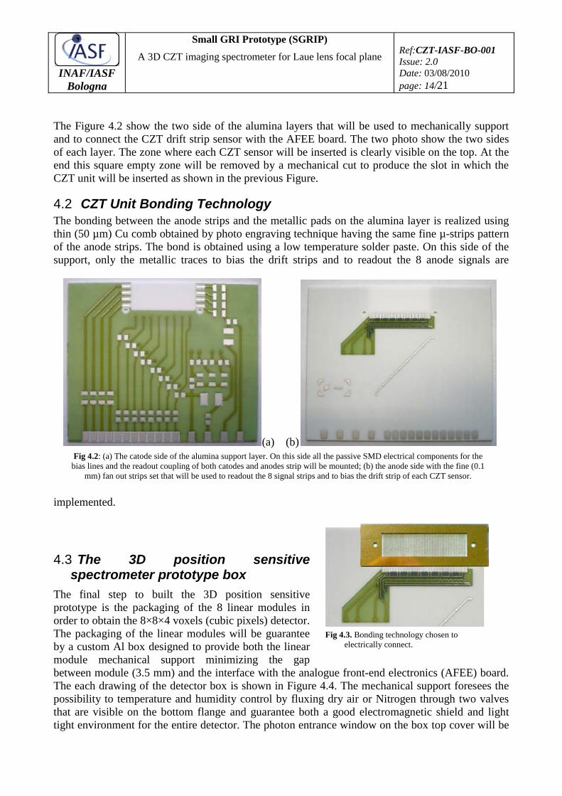
The Figure 4.2 show the two side of the alumina layers that will be used to mechanically support and to connect the CZT drift strip sensor with the AFEE board. The two photo show the two sides of each layer. The zone where each CZT sensor will be inserted is clearly visible on the top. At the end this square empty zone will be removed by a mechanical cut to produce the slot in which the CZT unit will be inserted as shown in the previous Figure.
4.2 CZT Unit Bonding Technology The bonding between the anode strips and the metallic pads on the alumina layer is realized using thin (50 µm) Cu comb obtained by photo engraving technique having the same fine µ-strips pattern of the anode strips. The bond is obtained using a low temperature solder paste. On this side of the support, only the metallic traces to bias the drift strips and to readout the 8 anode signals are
implemented.
4.3 The 3D position sensitive spectrometer prototype box
The final step to built the 3D position sensitive prototype is the packaging of the 8 linear modules in order to obtain the 8×8×4 voxels (cubic pixels) detector. The packaging of the linear modules will be guarantee by a custom Al box designed to provide both the linear module mechanical support minimizing the gap between module (3.5 mm) and the interface with the analogue front-end electronics (AFEE) board. The each drawing of the detector box is shown in Figure 4.4. The mechanical support foresees the possibility to temperature and humidity control by fluxing dry air or Nitrogen through two valves that are visible on the bottom flange and guarantee both a good electromagnetic shield and light tight environment for the entire detector. The photon entrance window on the box top cover will be
(a) (b) Fig 4.2: (a) The catode side of the alumina support layer. On this side all the passive SMD electrical components for the
bias lines and the readout coupling of both catodes and anodes strip will be mounted; (b) the anode side with the fine (0.1 mm) fan out strips set that will be used to readout the 8 signal strips and to bias the drift strip of each CZT sensor.
Fig 4.3. Bonding technology chosen to
electrically connect.

INAF/IASF
Bologna
Small GRI Prototype (SGRIP)
A 3D CZT imaging spectrometer for Laue lens focal plane Ref:CZT-IASF-BO-001 Issue: 2.0 Date: 03/08/2010 page: 15/21
realized using a 0.1 mm thick Be layer of 25×45 mm2 in order to reduce the photon absorption at low energies (<10 keV). The flinge between the detector top cover and the box is provided by an o-ring to guarantee a perfect light protection. Each CZT linear module is keep in position through Teflon guides that grab the Al2O3 layer at the empty space (10 mm) leaved on each vertical side. This solution will allow an easy insertion and extraction of each linear module in and from the electrical connectors aligned below the detector on the analogue front end electronics board. The detector box is directly bolted to the AFEE board trough a metallic contact that provides a separate ground
5 The Analog Front-end electronics The main function of the analogue front-end electronics (AFEE) is to connect the 64 anode strips and the 32 cathodes to three RENA-3 ASIC from NOVA R&D Inc. (CA, USA) used as signal readout devices. The RENA-3 ASIC is a 36-channel charge sensitive amplifier self-triggering. Each channel includes a low-noise preamplifier, a shaper with sample/hold, and in addition a fast shaper that gives a trigger signal for coincident event detection. The signal range is selectable channel by channel over two full scales (equivalent to 200 keV and 1.3 MeV for CZT) as the peaking time that ranges from 0.1 to 40 μs. The comparator thresholds can be adjusted through an 8 bit DAC on each channel in order to obtain an accurate and uniform threshold setting. A pole-zero cancellation circuit is available for minimizing pileup errors. All these features are selectable by software and are independent for each input channel. Main features:
-two optimizations for detector capacitance (2pF and 9pF); -the comparator thresholds are individually adjustable through an 8 bit DAC on each channel; -input signal polarity, peaking time (from 0.3 to 40 µs) and gain are selectable channel-by-channel; -low-EMI on digital interface; -power consumption: 6.5 mW/channel.
Readout modes:
-sparse, neighbor and global; -follower, to monitor in continuous mode the analog output shape of each channel.
(a) (b) Fig 4.4. The 3D position sensitive spectrometer prototype packaging (a) and the overall view of the detector box (b)
with the Be window and N/Dry air flux pipe on the bottom flange.

INAF/IASF
Bologna
Small GRI Prototype (SGRIP)
A 3D CZT imaging spectrometer for Laue lens focal plane Ref:CZT-IASF-BO-001 Issue: 2.0 Date: 03/08/2010 page: 16/21
Preliminary measurements were performed using a demo board, illustrated in Figure 5.2, developed to test the chip functionalities before the final implementation on the AFFE. This demo board is composed of two parts: the CPU board on the left and the Rena-3 board on the right. The CPU manages the ASIC configuration and receives the output data using a custom acquisition software. The RENA-3 board provides the low bias voltages (DAC reference voltages and power supplies), calibration pulser and CPU interface. Furthermore, the monitors of the pulser signal and the Rena-3 analog output are available. The dynamic range was determined by charge injection using a voltage step at the test input, which feeds a ~75 fF internal capacitor that can be switched to any input channel. Figure 5.3a reports the output amplitude measured for the minimum and maximum gain as a function of the injecting charge. The measured dynamic range for gain 1.6 is linear up to 36 fC and the chip output saturates at ~ 40 fC (1.15 MeV), for gain 5 the dynamic range is linear up to 9 fC and the chip output saturates at ~ 15 fC (435 keV). The distribution of the noise and offset values is shown in Figure 5.3b-c: the gaussian fit gives a noise of (8.95 ± 0.50) keV and an offset mean value of (-673.62 ± 11.86) mV. In the AFEE several other functions are implemented such as the detector high voltage power supply, the low voltage power supply, the conditioning electronics, the low and high voltage monitors, two temperature and humidity sensors for monitoring the detector and electronics environmental operating conditions.
Fig 5.1. Gain dispersion of 36 channels on the left. Behavior of the noise values divided by their gain on the right.
τ = 3 µs
Channel
0 10 20 30 40
Ampl
itude
(mV/
fC)
0
100
200
300
400
500x 1.6x 1.8x 2.3 x 5.0
τ = 3 µs
Channel
0 10 20 30 40
Noise
/gain
(mV)
0
5
10
15
20
25
30x 1.6x 1.8x 2.3 x 5.0
INAF/IASF
Bologna
Small GRI Prototype (SGRIP)
A 3D CZT imaging spectrometer for Laue lens focal plane Ref:CZT-IASF-BO-001 Issue: 2.0 Date: 03/08/2010 page: 17/21
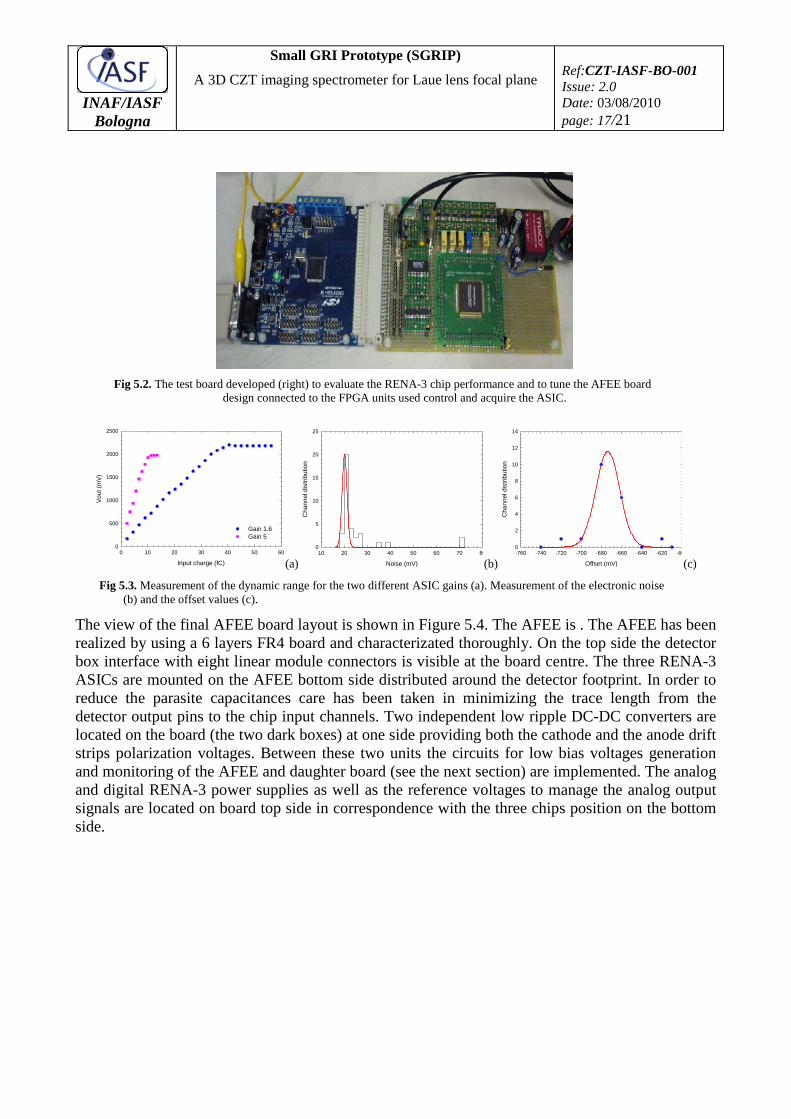
The view of the final AFEE board layout is shown in Figure 5.4. The AFEE is . The AFEE has been realized by using a 6 layers FR4 board and characterizated thoroughly. On the top side the detector box interface with eight linear module connectors is visible at the board centre. The three RENA-3 ASICs are mounted on the AFEE bottom side distributed around the detector footprint. In order to reduce the parasite capacitances care has been taken in minimizing the trace length from the detector output pins to the chip input channels. Two independent low ripple DC-DC converters are located on the board (the two dark boxes) at one side providing both the cathode and the anode drift strips polarization voltages. Between these two units the circuits for low bias voltages generation and monitoring of the AFEE and daughter board (see the next section) are implemented. The analog and digital RENA-3 power supplies as well as the reference voltages to manage the analog output signals are located on board top side in correspondence with the three chips position on the bottom side.
Fig 5.2. The test board developed (right) to evaluate the RENA-3 chip performance and to tune the AFEE board
design connected to the FPGA units used control and acquire the ASIC.
(a) (b) (c)
Fig 5.3. Measurement of the dynamic range for the two different ASIC gains (a). Measurement of the electronic noise (b) and the offset values (c).
Input charge (fC)
0 10 20 30 40 50 60
Vout
(mV)
0
500
1000
1500
2000
2500
Gain 1.6Gain 5
Noise (mV)
10 20 30 40 50 60 70 80
Cha
nnel
dis
tribu
tion
0
5
10
15
20
25
Offset (mV)
-760 -740 -720 -700 -680 -660 -640 -620 -60
Cha
nnel
dis
tribu
tion
0
2
4
6
8
10
12
14

INAF/IASF
Bologna
Small GRI Prototype (SGRIP)
A 3D CZT imaging spectrometer for Laue lens focal plane Ref:CZT-IASF-BO-001 Issue: 2.0 Date: 03/08/2010 page: 18/21
The RENA-3 analog output signals are buffered and sent to daughter card ADCs. An additional feature of the AFEE board is the capability of calibrating each ASIC channel using an on board pulser. The horizontal box highlights the I/O high density connectors to the data handling electronics. The maximum expected AFEE power consumption is ~15 W.
6 The Data Handling Electronics System The Data Handling Electronics (DHE) is composed of a daughter board (SG_ADC) that provides the interface between the AFEE and main digital processing board (SG_DGT). It
s functional scheme is shown in Figure 6.1. The DHE manages the detector high voltage power supply, the analog signal offset level A/D converters, the ASIC parameters configuration, the coincidence logics, the detector operational parameters, and finally prepares the output data stream
Fig 5.4. The final layout of the AFEE board: (a) top view from the detector box; (b) bottom view.
Fig 6.1. The functional and configuration scheme of the Data Handling Electronics (DHE) system. The two box
highlighted by thick border are the two DHE subsystems, while the one at right represent the AFEE board.

INAF/IASF
Bologna
Small GRI Prototype (SGRIP)
A 3D CZT imaging spectrometer for Laue lens focal plane Ref:CZT-IASF-BO-001 Issue: 2.0 Date: 03/08/2010 page: 19/21
using a programmable data format (LABVIEW compatible). The DHE system is based on a FPGA with embedded Power PC (PPC) and will be able to handle up to 128 independent channels via an Ethernet link. The daughter board (Figure 6.2) is placed on top of the SG_DGT one in the same metallic container and provides the interface circuits between the SG_DGT and the AFEE board, as well as the DAC and the ADC conversions. The main interface circuits consist of galvanic isolators for the digital signals from the SG_DGT to the AFEE board. One fast DAC is used to calibrate each RENA-3 channel, while others DACs set the high voltage values and the ADC read the high voltage analog monitors. Finally, the daughter board provides the A/D conversion of the RENA-3 analog signals. In table 6.1 we report the main characteristics of the DHE.
Maximum power consumption ~5 Watts
4 Connectors high density / 50 pins Table 6.1 DHE main characteristics (SG_ADC+ SG_DGT) The digital processing board (Figure 6.3) implement a Xilinx Virtex5 FPGA with embedded PPC and up to 2GB of local memory to manage the chip functionalities through an 1G Ethernet connection. Each acquisition module, composed of the RENA-3 ASIC and relative ADC, is managed by an IP-core that allows to adjust the ASIC settings, processes the received data and sends it to remote PC via Ethernet performing the data formatting. In particular, the SG_DGT can operate in coincidence mode acquiring events with any multiplicity in a selectable window from 1 to 20 μs. The full operating configuration can be store in the flash memory and reloaded automatically at every system startup. The digital processing board has been designed to manage up to 50k events/sec.
Fig 6.3. The digital processing board (SG_DGT). At the right it is visible the connector to the daughter board.
Fig 6.2. The daughter board

INAF/IASF
Bologna
Small GRI Prototype (SGRIP)
A 3D CZT imaging spectrometer for Laue lens focal plane Ref:CZT-IASF-BO-001 Issue: 2.0 Date: 03/08/2010 page: 20/21
7 Functional & Integration Test We are working to design the cooling system needed in order to obtain the optimum performance. Meanwhile we have tested a linear module to verify its functionality and to study the uniformity of the several readout strips by irradiating the CZT sensor with collimated radioactive sources of 109Cd, 241Am, 57Co and 137Cs. In following figures, we present a few spectra of 109Cd, that emits two main lines at ~22 and 88 keV, that show the performance of one CZT linear module with drift strips bians on and off (right), and the response of the anodic strips at temperature higher than 25° C (left).
8 Conclusions Currently almost all the prototype subsystems and mechanics are under construction and their delivery is foreseen within a working month. Only concerning the linear module realisation there are still some preliminary activities undergoing to verify the validity of the chosen bonding technique with some dummy CZT sensors realized by the IMEM/CNR group13. We foresee the integration and functional tests of AFEE and DHE in the next September, while we expect to have all the CZT linear modules ready to be implemented in the prototype a month later. The laboratory performance tests using radioactive sources, of the 3D CZT prototype could therefore start within the end of this year. Meanwhile we intend to submit a proposal to ESRF in Grenoble (France) to perform measurements with a high energy (50-700 keV) polarised photon beam at the line ID15A. The features of this beam line will allow us to characterise, over a wide energy range, with different beam size and as function of the photon incidence angles, our prototype in imaging capabilities, spectroscopic performance and effectiveness as scattering polarimeter. An important activity, that is held in parallel with the construction of the prototype, is the implementation in GEANT 4 of a numerical model of the final 3D prototype to perform MC simulations dedicated to made prevision and to help in the understanding of the results that will we obtain during the prototype performance tests.
Fig 7.1. (left) Comparison between the 109Cd spectra acquired without (blue) and with (pink) bias voltage applied to the drift strips surrounding the readout anode strip; (right) Collimated 109Cd spectra acquired at a temperature higher than 25 °C.
109Cd
Channels0 50 100 150 200 250 300
Cou
nts
0
500
1000
1500
2000
2500
Without drift strip bias voltageApplied drift strip bias voltage
Channels
0 50 100 150 200 250 300
Cou
nts
0
20
40
60
80
100
109Cd
Channels0 50 100 150 200 250 300
Coun
ts
0
2000
4000
6000
8000
10000
12000
14000Strip 1 Strip 2 Strip 3 Strip 4 Strip 5 Strip 6 Strip 7 Strip 8
Channels
0 50 100 150 200 250 300
Coun
ts
0
50
100
150
200
250
300

INAF/IASF
Bologna
Small GRI Prototype (SGRIP)
A 3D CZT imaging spectrometer for Laue lens focal plane Ref:CZT-IASF-BO-001 Issue: 2.0 Date: 03/08/2010 page: 21/21
REFERENCES
1. Cosmic Vision: Space Science for Europe 2015-2025, ESA Brochure Volume BR-247, pp. 1-111 (2005) (http://sci.esa.int/science-e/www/object/index.cfm?fobjectid=38542#).
2. Frontera, F., et al., “Focusing of gamma-rays with Laue lenses: first results”, Proc. SPIE 7011, 70111R 1-8 (2008). 3. Gehrels, N., et al., “The Swift Gamma-Ray Burst Mission”, The Astrophysical Journal 711(2), 1005–1020 (2004). 4. Lebrun, F., et al., “ISGRI : a CdTe array imager for INTEGRAL”, Proc. SPIE 2806, 258-268 (1996). 5. Meuris, A., et al., “Caliste 64, an Innovative CdTe Hard X-Ray Micro-Camera”, IEEE Trans. on Nucl. Sci. 55(2),
778-784 (2008). 6. Curado da Silva, R.M., et al., “Polarimetric performance of a Laue lens gamma-ray CdZnTe focal plane prototype”,
Journal of Applied Physics 104, 084903 1-7 (2008). 7. Knödlseder, J., et al., “GRI: focusing on the evolving violent universe”, Experimental Astronomy, 23, pp. 121-138
(2009). 8. Casali, F., et al., “Characterization of small CdTe detectors to be used for linear and matrix arrays”, IEEE Trans. on
Nucl. Sci. 39(4), 598-604 (1992). 9. Van Pamelen, M.A.J., Budtz-Jørgensen, C. and Kuvvetli, I., “Development of CdZnTe X-ray detectors at DSRI”,
Nucl. Instr. and Meth. in Phys Res. A 439, 625-633 (2000). 10. Gostilo, V., et al., “The development of drift-strip detectors based on CdZnTe”, IEEE Trans. on Nucl. Sci. 49(5),
2530-2534 (2002). 11. Dusi, W, et al., “Spectroscopic behavior of CdTe detectors as a function of the inter-electrode distance”, Proc. SPIE
3768, 88-97 (1999). 12. Zappettini, A., et al., “Boron oxide encapsulated vertical bridgman grown CdZnTe crystals as X-Ray detector
material”, IEEE Trans. on Nucl. Sci. 56(4), 1743-1746 (2009).