spadic v0.3 and v1
TRANSCRIPT

SchaltungstechnikSimulationund
SchaltungstechnikSimulationund
SPADIC v0.3 and v1.0
FEE/DAQ Meeting @ FIAS (Frankfurt)
November 2010
Self-triggered Pulse Amplification and Digitization asIC

Nov. 2010 FEE/DAQ Meeting - Tim Armbruster 2LS Schaltungstechnik & Simulation
SchaltungstechnikSimulationund
1. Latest Chip Architecture (v0.3)

Nov. 2010 FEE/DAQ Meeting - Tim Armbruster 3LS Schaltungstechnik & Simulation
SchaltungstechnikSimulationund
Block Diagram of Current ASIC
preamp 25 shaper 25
SR 0preamp 0 shaper 0
ADC 0
Analog Bias12 x 7 Bit current DAC
Shift RegisterControl
8
8
8
8
8
8
8
8
Output MUXand
Decoder16
9
Testand
CalibrationCircuits
ADC 7 SR 7
ESD Pad
ESD Pad
ESD Pad
ESD Pad
ESD Pad
ESD Pad
ESD Pad
ESD Pad
8 complete channels (ESD pad, CSA, ADC, output decoder)

Nov. 2010 FEE/DAQ Meeting - Tim Armbruster 4LS Schaltungstechnik & Simulation
SchaltungstechnikSimulationund
Reminder: Preamplifier/Shaper Circuit
H s ≈ADC
1sRSCS2
RS RS
CS
CS
11x 1x
(also channels with less
instances for test purpose
on chip)
• O'Connor FB
• 2nd order shaper
• Shaping time: 82 ns
• Unified amplifier cell
• N-MOS input
• ≈ 3.6 mW/channel
New:
• Scaled lengths of input NMOS (180, 250, 320, 390, 460nm)
• Re-Layout of input NMOS: The (long) gate-fingers have been cut into smaller pieces to decrease gate resistance

Nov. 2010 FEE/DAQ Meeting - Tim Armbruster 5LS Schaltungstechnik & Simulation
SchaltungstechnikSimulationund
Reminder: Algorithmic ADC Design
U to I
compa-rator
currentin/out
write
write & read
Vref digitalout
current mode
voltage node
digital domain
storage node
• 8 (scaled) pipeline stages, therefore 9 Bit design, 7.5 Bits effective so far
• Algorithmic working principle (“1.5 redundant Bits” / conversion step)
• 25 MSamples/s, layout only 130x120 µm², power consumption 4.5 mW
• Core unit: Novel current storage cell:

Nov. 2010 FEE/DAQ Meeting - Tim Armbruster 6LS Schaltungstechnik & Simulation
SchaltungstechnikSimulationund
Current Test-Chip: Layout
Bias circuitry (12 current DACs)26 preamp/shaper channelsDetector capacitors (5pF per block)8 pipelined ADCs
ADC control + bias 5.2 kBit shift register matrixControl + readout/decoder logic blocksTest circuits

Nov. 2010 FEE/DAQ Meeting - Tim Armbruster 7LS Schaltungstechnik & Simulation
SchaltungstechnikSimulationund
Typical Analog Shaper Pulse
Analog shaper output pulse

Nov. 2010 FEE/DAQ Meeting - Tim Armbruster 8LS Schaltungstechnik & Simulation
SchaltungstechnikSimulationund
Preamp/Shaper Noise
Measurement
Simulation
750e ENC @ 30pF
(still)
prelim
inary
• New layout of input NMOS had no impact on noise results
• Large deviation between channel types can't be seen in simulation
• 320nm is the best choice
Nov. 2010 FEE/DAQ Meeting - Tim Armbruster 9LS Schaltungstechnik & Simulation
SchaltungstechnikSimulationund
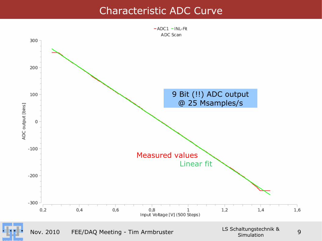
Characteristic ADC Curve
9 Bit (!!) ADC output@ 25 Msamples/s
Measured valuesLinear fit

Nov. 2010 FEE/DAQ Meeting - Tim Armbruster 10LS Schaltungstechnik & Simulation
SchaltungstechnikSimulationund
ADC's DNL and INL
DNL < 1 Bit ADC res. > 8 Bit→
INL ~ 1.5 Bit ADC res. ~ 7.5 Bit→
Current ADC resolution of about 7.5 Bit(In sigma the values above would even look better)
@ 25 Msamples/s (40 ns sample period)
DNL < 1 Bit ADC res. > 8 Bit→

Nov. 2010 FEE/DAQ Meeting - Tim Armbruster 11LS Schaltungstechnik & Simulation
SchaltungstechnikSimulationund
First (yet noisy) digitized pulses
Pulses for different input charges
Amplitude histogram of fitted curves
Smaller due to poor fit algorithm
Pulses with new setup look even much smoother (see next slides), but no measurement available yet :-(
Old Setup

Nov. 2010 FEE/DAQ Meeting - Tim Armbruster 12LS Schaltungstechnik & Simulation
SchaltungstechnikSimulationund
(Old) Pre-Testbeam Setup

Nov. 2010 FEE/DAQ Meeting - Tim Armbruster 13LS Schaltungstechnik & Simulation
SchaltungstechnikSimulationund
2. Testbeam Setup

Nov. 2010 FEE/DAQ Meeting - Tim Armbruster 14LS Schaltungstechnik & Simulation
SchaltungstechnikSimulationund
Testbeam Setup Overview• “Old” chip (Spadic v0.3) but …
– New front-end PCB
• Low-noise layout, several smaller improvements
• Harwin ZIF connector compatible (same connector type as in ALICE TRD)
– New FPGA readout controller (Susibo)
• Virtex 5, 2MB SRAM, FTDI (USB 2.0), EEPROM(s), ...
– New firmware
• High readout rate of up to 8k events/s (368 Byte/event)
• Package based protocol
• New Features like local time-stamp, external event-id extraction (sync-t), …
– New Software-Library
• Provides abstract functions like (dis-)connect(), readNextPackage(), status(), …
• Necessary for integration in DABC framework
– New stand-alone readout client (hitclient)
• Beamtime target: 8 completely running Setups (8 channels each)
– Last-minute point landing, also the Susibo was “just in time”
– A lot of problems with assembly and bonding
=> Finally 8 setups worked (most of the beam-time only 6 were run in parallel)

Nov. 2010 FEE/DAQ Meeting - Tim Armbruster 15LS Schaltungstechnik & Simulation
SchaltungstechnikSimulationund
SPADIC plugged on Susibo
SPADIC
To TRD
Power
Power daisy-chain
Ext trigger input (sync-t)
Susibo

Nov. 2010 FEE/DAQ Meeting - Tim Armbruster 16LS Schaltungstechnik & Simulation
SchaltungstechnikSimulationund
Setup in Lab
2 Hitclients with live-data
2 SPADIC Setups
Test pulses injected trough test pulse generator on PCB

Nov. 2010 FEE/DAQ Meeting - Tim Armbruster 17LS Schaltungstechnik & Simulation
SchaltungstechnikSimulationund
Hitclient Screenshot

Nov. 2010 FEE/DAQ Meeting - Tim Armbruster 18LS Schaltungstechnik & Simulation
SchaltungstechnikSimulationund
Frankfurt's TRD-SPADIC Setup
Sorry, problem with my digi-cam :-(

Nov. 2010 FEE/DAQ Meeting - Tim Armbruster 19LS Schaltungstechnik & Simulation
SchaltungstechnikSimulationund
Münster's TRD-SPADIC Setup
2 Münster's ALICE-Style chambers with drift
4 SPADIC Setups

Nov. 2010 FEE/DAQ Meeting - Tim Armbruster 20LS Schaltungstechnik & Simulation
SchaltungstechnikSimulationund
Setup in the Experimental Hall
Sorry, problem with my digi-cam :-(

Nov. 2010 FEE/DAQ Meeting - Tim Armbruster 21LS Schaltungstechnik & Simulation
SchaltungstechnikSimulationund
3. First Testbeam Results

Nov. 2010 FEE/DAQ Meeting - Tim Armbruster 22LS Schaltungstechnik & Simulation
SchaltungstechnikSimulationund
Results from an electronic's point of view
• Bad :-(
– Many problems with pickup (external noise) – a lot of effort was necessary to reduce the different kinds of oscillation to a tolerable minimum
– Even after “optimization” some boards still showed strong oscillations
– (Due to known reasons) the chip's configuration was very unstable – a lot of re-configurations/restarts were necessary
– Strange baseline-shift (DC-level) of shaper outputs if detectors were connected AND the ADCs were running (yet there was no time to investigate this)
• Good :-)
– 8 Spadic/Susibo setups finished just in time
– Successful integration of Spadic software library into DABC (thanks to Sergey and Jörn)
– External triggering-scheme worked well
– Finally 6 working Spadic setups in parallel (4 x Münster, 2x Frankfurt)
– A lot of nice hits could be recorded (but also some ugly)
Nov. 2010 FEE/DAQ Meeting - Tim Armbruster 23LS Schaltungstechnik & Simulation
SchaltungstechnikSimulationund
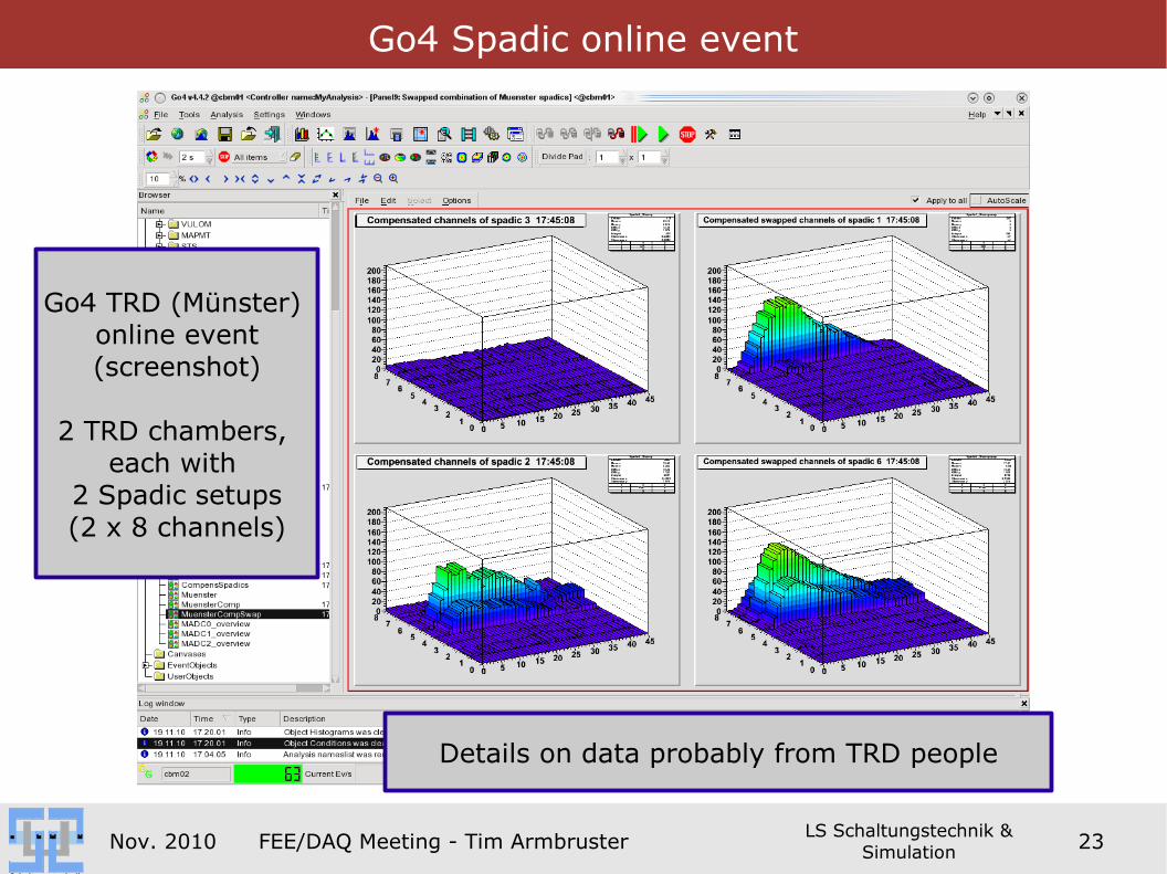
Go4 Spadic online event
Go4 TRD (Münster) online event(screenshot)
2 TRD chambers, each with
2 Spadic setups(2 x 8 channels)
Details on data probably from TRD people

Nov. 2010 FEE/DAQ Meeting - Tim Armbruster 24LS Schaltungstechnik & Simulation
SchaltungstechnikSimulationund
4. Towards SPADIC v1.0
Nov. 2010 FEE/DAQ Meeting - Tim Armbruster 25LS Schaltungstechnik & Simulation
SchaltungstechnikSimulationund
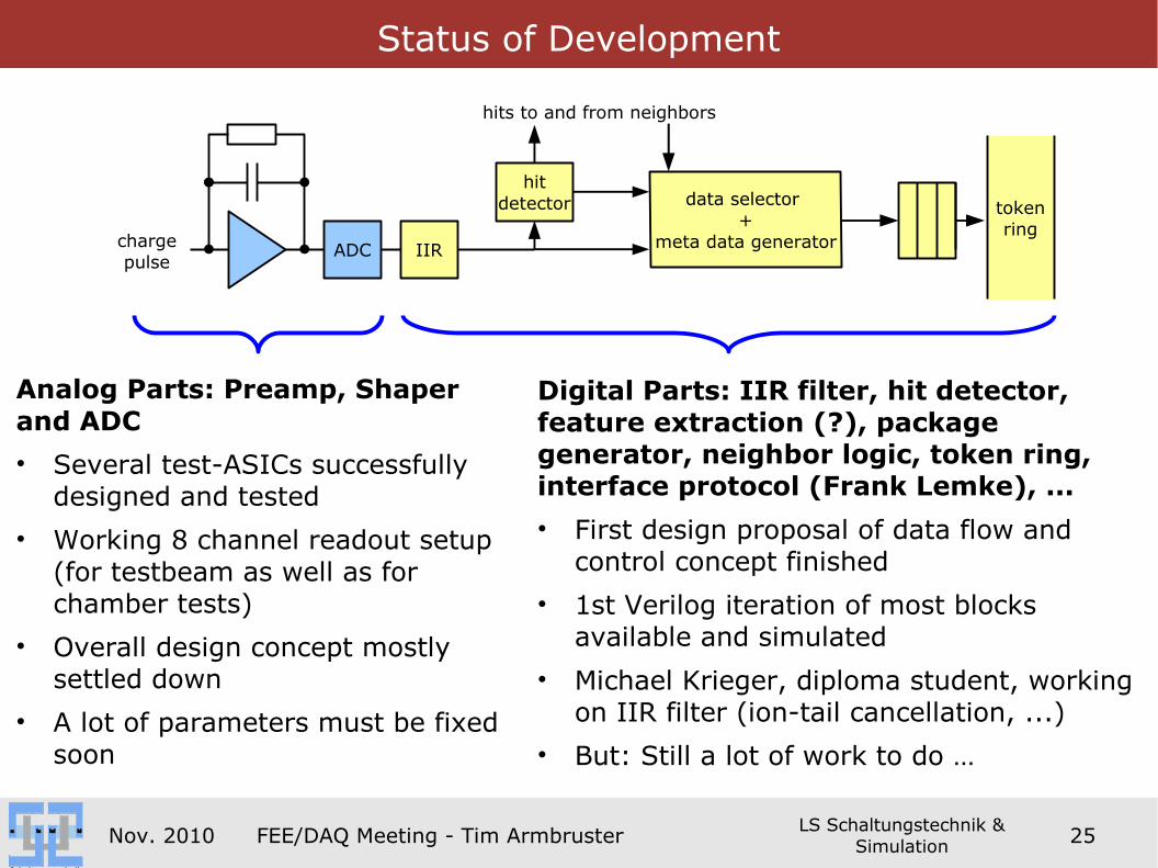
Status of Development
tokenring
ADC IIR
hitdetector
hits to and from neighbors
chargepulse
Analog Parts: Preamp, Shaper and ADC
• Several test-ASICs successfully designed and tested
• Working 8 channel readout setup (for testbeam as well as for chamber tests)
• Overall design concept mostly settled down
• A lot of parameters must be fixed soon
Digital Parts: IIR filter, hit detector, feature extraction (?), package generator, neighbor logic, token ring, interface protocol (Frank Lemke), ...
• First design proposal of data flow and control concept finished
• 1st Verilog iteration of most blocks available and simulated
• Michael Krieger, diploma student, working on IIR filter (ion-tail cancellation, ...)
• But: Still a lot of work to do …

Nov. 2010 FEE/DAQ Meeting - Tim Armbruster 26LS Schaltungstechnik & Simulation
SchaltungstechnikSimulationund
Conceptual Data Flow Diagram
tokenring
prev.chip
nextchip
ADC IIR
hitdetector
hits to and from neighbors
chargepulse
digitalanalog
output logic
+driver

Nov. 2010 FEE/DAQ Meeting - Tim Armbruster 27LS Schaltungstechnik & Simulation
SchaltungstechnikSimulationund
Spadic 1.0: Preamplifier / Shaper
• Charge sensitive preamplifier (CSA)
– Single ended, N-MOS input
– Input protection
– Switchable polarity
– Switchable # amplifier cells
• Shaper
– 2nd order, PZ-cancellation, 82 ns
– Switchable shaping-time
– Increased order
• Both
– 750e ENC @ 30 pF, 3.8 mW
– Switchable gain
Already AvailablePlanned featurePossible feature

Nov. 2010 FEE/DAQ Meeting - Tim Armbruster 28LS Schaltungstechnik & Simulation
SchaltungstechnikSimulationund
Spadic 1.0: ADC
• Pipeline ADC, continuously running
– Current-mode algorithmic ADC
– 9 Bit design, 7.5 Bit effective
– Up to 25 Msamples/s
– 4.5 mW / rad-tolerant
– Slightly better resolution (~ 8 Bit)
– High resolution (> 8 Bit), possible but very expensive in terms of man-power, power consumption, chip area, …
– Improved DC-Level / baseline adjustment mechanism Already Available
Planned featurePossible feature
Nov. 2010 FEE/DAQ Meeting - Tim Armbruster 29LS Schaltungstechnik & Simulation
SchaltungstechnikSimulationund
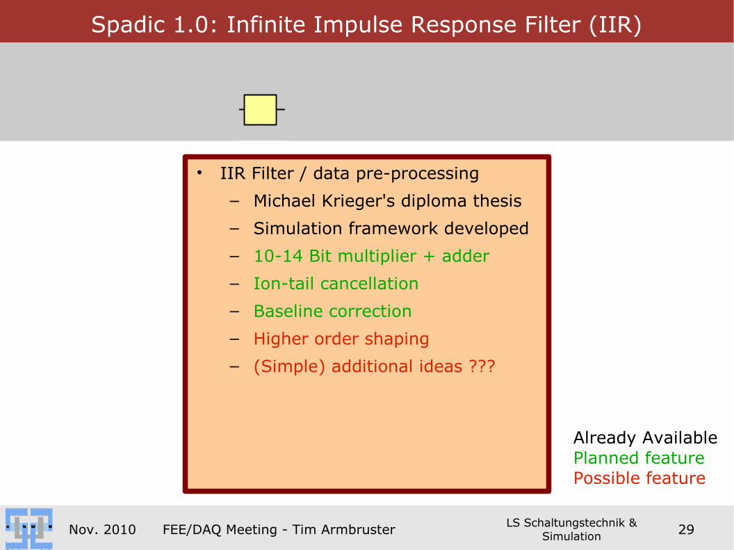
Spadic 1.0: Infinite Impulse Response Filter (IIR)
• IIR Filter / data pre-processing
– Michael Krieger's diploma thesis
– Simulation framework developed
– 10-14 Bit multiplier + adder
– Ion-tail cancellation
– Baseline correction
– Higher order shaping
– (Simple) additional ideas ???
Already AvailablePlanned featurePossible feature

Nov. 2010 FEE/DAQ Meeting - Tim Armbruster 30LS Schaltungstechnik & Simulation
SchaltungstechnikSimulationund
Spadic 1.0: Hit Detector and Neighbor Trigger
• Digital hit detector
– Digital hit extraction logic
– Different hit extraction schemes (threshold, double threshold, pulse length, …)
– 1th order Verilog, simulation works
• Neighbor readout logic
– Automatic readout of neighbor channels
– Trigger signal across chip edges
– 1th order Verilog, simulation works
Already AvailablePlanned featurePossible feature

Nov. 2010 FEE/DAQ Meeting - Tim Armbruster 31LS Schaltungstechnik & Simulation
SchaltungstechnikSimulationund
Spadic 1.0: Meta Data Generator and Package Builder
• Meta Data Generator
– Local and external time-stamp extraction
– Hit type extraction (internal, neighbor, …)
– Channel #, Chip ID, …
– 1th order Verilog, simulation works
• Package builder
– Generation of hit package including meta and hit data
– 1th order Verilog, simulation works
Already AvailablePlanned featurePossible feature

Nov. 2010 FEE/DAQ Meeting - Tim Armbruster 32LS Schaltungstechnik & Simulation
SchaltungstechnikSimulationund
Spadic 1.0: Output Interface
• Output Interface
– FIFO package buffer
• Need access to some UMC 018 SRAM generator
– Token ring inter-channel network
– Sophisticated deterministic latency output protocol (Frank Lemke)
– CBM DAQ compatible !!!
– Serializer
– Output driverAlready AvailablePlanned featurePossible feature

Nov. 2010 FEE/DAQ Meeting - Tim Armbruster 33LS Schaltungstechnik & Simulation
SchaltungstechnikSimulationund
Digital Hit Detector and Package Builder
input buffer(FIFO)
input buffer(FIFO)
hit synchronization
hit synchronization
hitdetector
hitdetector
meta data generator (logic only)
meta data generator (logic only)
main control(FSM)
main control(FSM)
start of frameFIFO
start of frameFIFO
IIR data (9)
threshold (9)
hit length (6)
max hit length (6)
neighbor hits (2)
internal hit (1)
hit
hit type (2),TS latched (12)
data selector
data selector
output buffer (FIFO)
output buffer (FIFO)
start of frameFIFO
start of frameFIFO
# values sent (6),control (9) write enable (2),
almost full (2)
global TS (12)
inte
r ch
annel
net
work
(to
ken r
ing)
meta data (9)mixed data (10)
select (1)

Nov. 2010 FEE/DAQ Meeting - Tim Armbruster 34LS Schaltungstechnik & Simulation
SchaltungstechnikSimulationund
Chip Concept
v1.0• Features on chip-level
– 32 channels / chip (maybe 64)
– Several test mechanisms (test injection, analog signal access, …)
– On-chip bias circuitry (current DACs + diodes)
– A lot of global and local configuration registers
– Maskable channels
– Power consumption / channel: analog ~ 10mW, digital ??? power limit?→
– Data: LVDS inputs / outputs only
– Additional channel as global reference to eliminate systematic disturbances (e.g. pick-up)
Planned featurePossible feature

Nov. 2010 FEE/DAQ Meeting - Tim Armbruster 35LS Schaltungstechnik & Simulation
SchaltungstechnikSimulationund
If Spadic also goes for RICH people ...
• Necessary adjustments of Spadic 1.0 concept for RICH (Ring Imaging Cherenkov)
– Much smaller input gain (max. 1.6 pC / hit) switchable preamp/shaper gain→
– Negative input charge bidirectional input stage→
– Very good time resolution ~ 2ns sophisticated feature extraction on-chip or offline→
• Is this time resolution achievable (40 ns sampling period)?
– Energy feature extraction on-chip (preferred) or offline (?)→
– Opt: more than 32 channels (>= 64)
• List not too long, but I'm already busy additional man-power on the horizon?→

Nov. 2010 FEE/DAQ Meeting - Tim Armbruster 36LS Schaltungstechnik & Simulation
SchaltungstechnikSimulationund
(Updated) Data-Rate Calculation
Some estimated numbers:
• 32 channels / chip
• 250 kHz maximum event rate / channel (one hit every 4 µs)
• 8 Bit ADC resolution
• 10 samples / event <= we need to further investigate here
• 12 Bit time-stamp / event (epoch length 164 µs @ 25MSamples/s ADC speed)
• 5 Bit channel ID
● => Conservative estimation: about 12 Bytes / (hit + channel)!● => Planned output protocol from computer architecture group (Ulrich Brüning
and Frank Lemke) foresees two links per chip with 500 Mbit/s each● Note: Epoch counter + forward error correction overhead not considered here!
Rchip =250k eventschannel⋅s
⋅ 32channels
hit ratechip
⋅ 8bit
sample⋅
10samplesevent
hit data
17bitevent
time−stampID
=776Mbit
s

Nov. 2010 FEE/DAQ Meeting - Tim Armbruster 37LS Schaltungstechnik & Simulation
SchaltungstechnikSimulationund
Floor Plan Proposal
Bias
Slow Control and Data I/O
Post
-Pro
cess
ing /
Rea
dout
Preamp/Shaper IIRInj. ADC
3 mm
2m
m
300µm
det
ecto
r ch
annel
pitch
Detector Pads Bias + Power Pads Digital I/O
Preamp/ShaperIIR Inj.ADC
● 3 x 2 mm² estimated die size● 32 channels, 80µm pitch, (mostly) symmetric layout for low(er) IR-drops● Detector connection-pads on two sides (chips will probably be attached to back of detector-
module, this relaxes routing/spacing)

Nov. 2010 FEE/DAQ Meeting - Tim Armbruster 38LS Schaltungstechnik & Simulation
SchaltungstechnikSimulationund
5. Future of the Test-Beam-Setup
Nov. 2010 FEE/DAQ Meeting - Tim Armbruster 39LS Schaltungstechnik & Simulation
SchaltungstechnikSimulationund
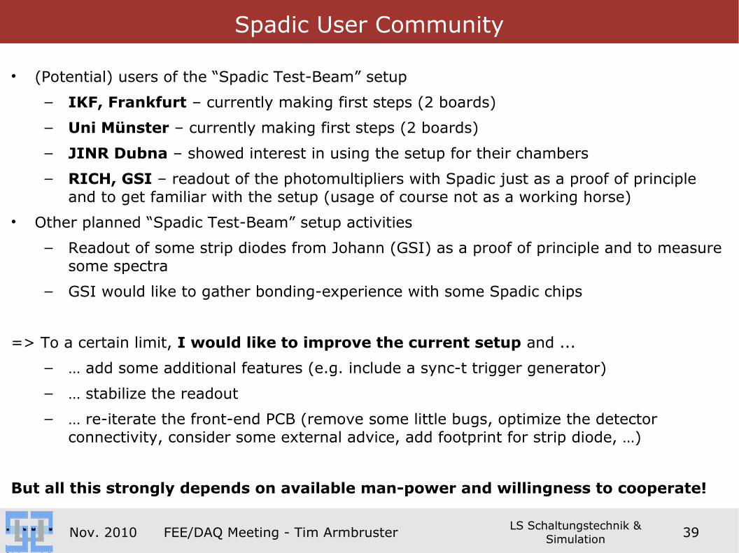
Spadic User Community
• (Potential) users of the “Spadic Test-Beam” setup
– IKF, Frankfurt – currently making first steps (2 boards)
– Uni Münster – currently making first steps (2 boards)
– JINR Dubna – showed interest in using the setup for their chambers
– RICH, GSI – readout of the photomultipliers with Spadic just as a proof of principle and to get familiar with the setup (usage of course not as a working horse)
• Other planned “Spadic Test-Beam” setup activities
– Readout of some strip diodes from Johann (GSI) as a proof of principle and to measure some spectra
– GSI would like to gather bonding-experience with some Spadic chips
=> To a certain limit, I would like to improve the current setup and ...
– … add some additional features (e.g. include a sync-t trigger generator)
– … stabilize the readout
– … re-iterate the front-end PCB (remove some little bugs, optimize the detector connectivity, consider some external advice, add footprint for strip diode, …)
But all this strongly depends on available man-power and willingness to cooperate!
Nov. 2010 FEE/DAQ Meeting - Tim Armbruster 40LS Schaltungstechnik & Simulation
SchaltungstechnikSimulationund
6. Next steps and timetable
Nov. 2010 FEE/DAQ Meeting - Tim Armbruster 41LS Schaltungstechnik & Simulation
SchaltungstechnikSimulationund
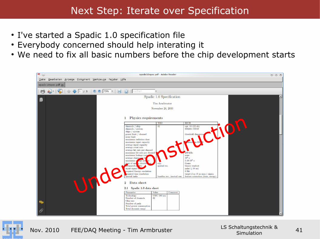
Next Step: Iterate over Specification
● I've started a Spadic 1.0 specification file● Everybody concerned should help interating it● We need to fix all basic numbers before the chip development starts
Under constru
ction

Nov. 2010 FEE/DAQ Meeting - Tim Armbruster 42LS Schaltungstechnik & Simulation
SchaltungstechnikSimulationund
Next Step: Debug and improve Testbeam-Setup
● We still need to understand …● … the strange baseline shift … ● … the high sensitivity to pick-up noise (PCB, chip or detector
problem?) …
● We probably should gather some more experience by …● … reading out some silicon strip detector … ● … (maybe) reading out the RICH photodiodes … ● … further improving the setup (see need to understand) …
… before we finish the Spadic 1.0 development.
Nov. 2010 FEE/DAQ Meeting - Tim Armbruster 43LS Schaltungstechnik & Simulation
SchaltungstechnikSimulationund
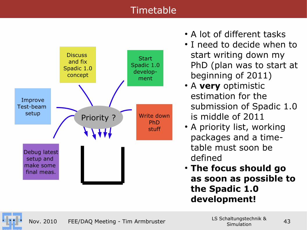
Timetable
ImproveTest-beam
setup
StartSpadic 1.0develop-
ment
Write downPhDstuff
Discuss and fix
Spadic 1.0concept
Debug latestsetup and
make some final meas.
Priority ?
● A lot of different tasks● I need to decide when to
start writing down my PhD (plan was to start at beginning of 2011)
● A very optimistic estimation for the submission of Spadic 1.0 is middle of 2011
● A priority list, working packages and a time-table must soon be defined
● The focus should go as soon as possible to the Spadic 1.0 development!
Nov. 2010 FEE/DAQ Meeting - Tim Armbruster 44LS Schaltungstechnik & Simulation
SchaltungstechnikSimulationund
5. Summary and Outlook

Nov. 2010 FEE/DAQ Meeting - Tim Armbruster 45LS Schaltungstechnik & Simulation
SchaltungstechnikSimulationund
Summary and Outlook
Status of the latest setup:
• 8 working Spadic v0.3 / Susibo setups
• Successful integration in CBM test-beam environment
• Promising results in lab and from test-beam but also open problems
• A lot of interest in using the current setup from different groups
Status of Spadic 1.0 design concept
• Complete design concept available
• Analog part (except for some improvements) conceptually completed
• Most digital building blocks still in a very early design phase
• Many features still need to be discussed
• Design kick-off as early as possible in 2011
Next Steps:
• Improve latest setup and gather more experience with chambers and silicon
• Discuss and fix specification
• Focus on Spadic 1.0 development

Nov. 2010 FEE/DAQ Meeting - Tim Armbruster 46LS Schaltungstechnik & Simulation
SchaltungstechnikSimulationund
You want to use this logo? Feel free to do so! Get it at http://cbm.uni-hd.de/daq/more/spadic/logo/