specifying digital circuits - courses.cs.washington.edu · bcd to gray code converter pals and...
TRANSCRIPT
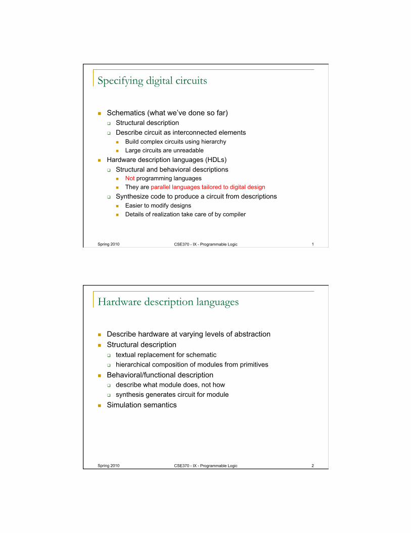
Specifying digital circuits
Schematics (what we’ve done so far) Structural description Describe circuit as interconnected elements
Build complex circuits using hierarchy Large circuits are unreadable
Hardware description languages (HDLs) Structural and behavioral descriptions
Not programming languages They are parallel languages tailored to digital design
Synthesize code to produce a circuit from descriptions Easier to modify designs Details of realization take care of by compiler
Spring 2010 1 CSE370 - IX - Programmable Logic
Spring 2010 CSE370 - IX - Programmable Logic 2
Hardware description languages
Describe hardware at varying levels of abstraction Structural description
textual replacement for schematic hierarchical composition of modules from primitives
Behavioral/functional description describe what module does, not how synthesis generates circuit for module
Simulation semantics
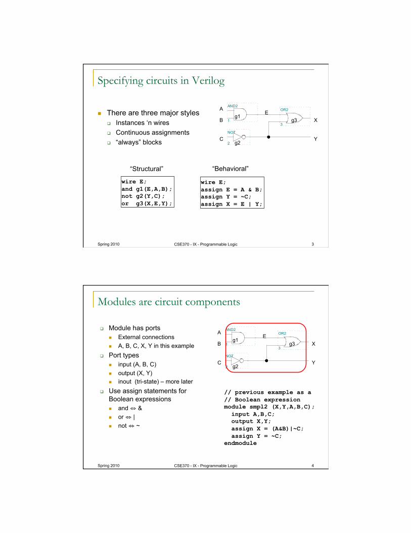
Specifying circuits in Verilog
There are three major styles Instances ‘n wires Continuous assignments “always” blocks
E
Cg2
Y
A
Bg1
g3 X
2
NOT
1
AND2
3
OR2
wire E; and g1(E,A,B); not g2(Y,C); or g3(X,E,Y);
wire E; assign E = A & B; assign Y = ~C; assign X = E | Y;
“Structural” “Behavioral”
Spring 2010 3 CSE370 - IX - Programmable Logic
Modules are circuit components
Module has ports External connections A, B, C, X, Y in this example
Port types input (A, B, C) output (X, Y) inout (tri-state) – more later
Use assign statements for Boolean expressions and ⇔ & or ⇔ | not ⇔ ~
// previous example as a // Boolean expression module smpl2 (X,Y,A,B,C); input A,B,C; output X,Y; assign X = (A&B)|~C; assign Y = ~C; endmodule
E
Cg2
Y
A
Bg1
g3 X
2
NOT
1
AND2
3
OR2
Spring 2010 4 CSE370 - IX - Programmable Logic
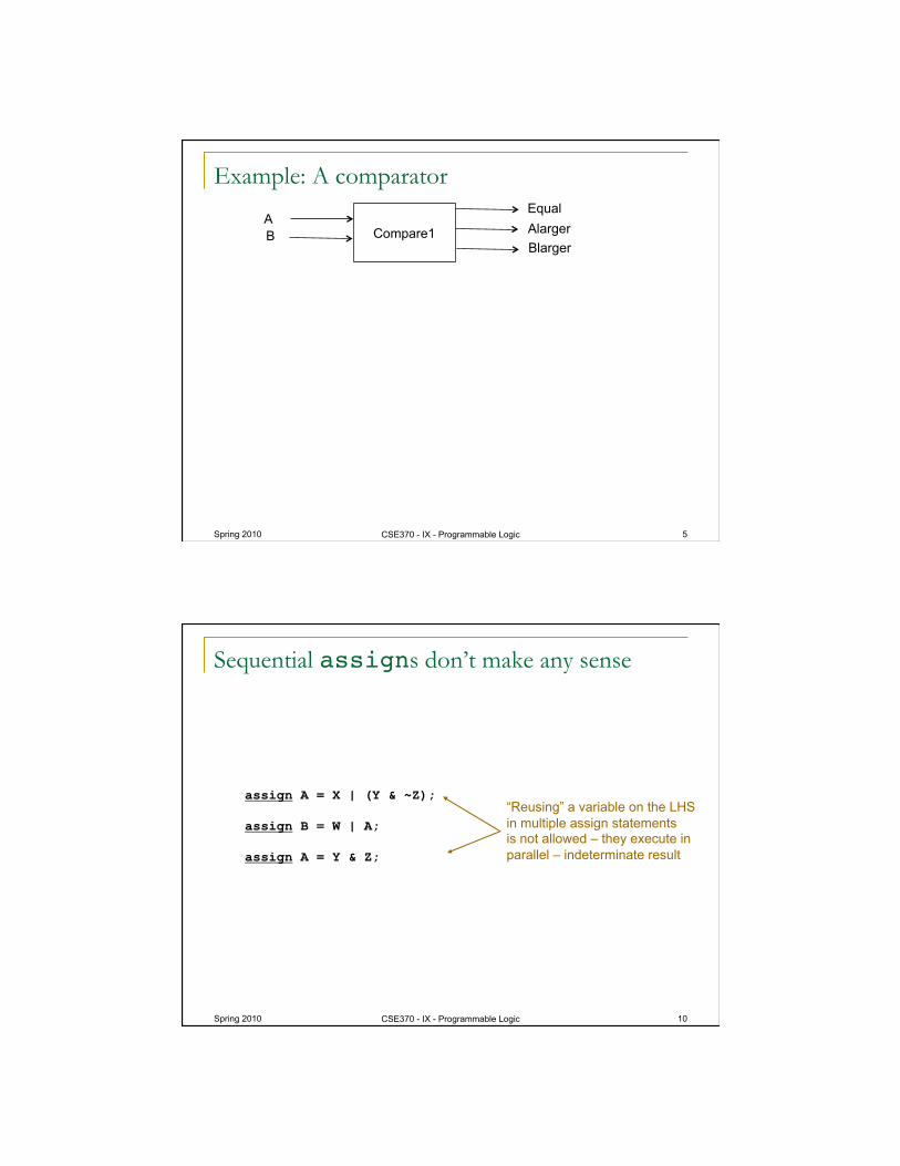
Example: A comparator
Spring 2010 5 CSE370 - IX - Programmable Logic
Compare1 A B
Equal Alarger Blarger
Sequential assigns don’t make any sense
assign A = X | (Y & ~Z);
assign B = W | A;
assign A = Y & Z;
“Reusing” a variable on the LHS in multiple assign statements is not allowed – they execute in parallel – indeterminate result
Spring 2010 10 CSE370 - IX - Programmable Logic
Spring 2010 CSE370 - IX - Programmable Logic 11
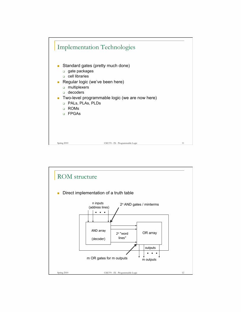
Implementation Technologies
Standard gates (pretty much done) gate packages cell libraries
Regular logic (we’ve been here) multiplexers decoders
Two-level programmable logic (we are now here) PALs, PLAs, PLDs ROMs FPGAs
Spring 2010 CSE370 - IX - Programmable Logic 12
ROM structure
Direct implementation of a truth table
(address lines)
• • •
n inputs
AND array
(decoder)
2n “word lines”
• • •
outputs
OR array
m outputs
2n AND gates / minterms
m OR gates for m outputs

Spring 2010 CSE370 - IX - Programmable Logic 13
ROM structure
A'B'C'
A'B'C
A'BC'
A'BC
AB'C'
AB'C
ABC'
ABC
A B C
F1 F2 F3 F0
AND array generates minterms Full decoder on the memory address
Connect minterms to OR gates
Spring 2010 CSE370 - IX - Programmable Logic 14
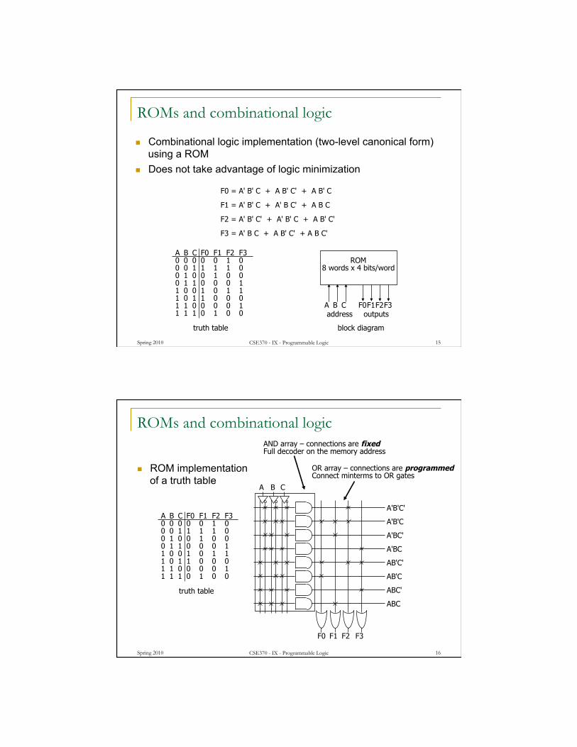
F0 = A' B' C + A B' C' + A B' C
F1 = A' B' C + A' B C' + A B C
F2 = A' B' C' + A' B' C + A B' C'
F3 = A' B C + A B' C' + A B C'
truth table
A B C F0 F1 F2 F3 0 0 0 0 0 1 0 0 0 1 1 1 1 0 0 1 0 0 1 0 0 0 1 1 0 0 0 1 1 0 0 1 0 1 1 1 0 1 1 0 0 0 1 1 0 0 0 0 1 1 1 1 0 1 0 0
block diagram
ROM 8 words x 4 bits/word
address outputs A B C F0 F1 F2 F3
ROMs and combinational logic
Combinational logic implementation (two-level canonical form) using a ROM
Does not take advantage of logic minimization
Spring 2010 CSE370 - IX - Programmable Logic 15
F0 = A' B' C + A B' C' + A B' C
F1 = A' B' C + A' B C' + A B C
F2 = A' B' C' + A' B' C + A B' C'
F3 = A' B C + A B' C' + A B C'
truth table
A B C F0 F1 F2 F3 0 0 0 0 0 1 0 0 0 1 1 1 1 0 0 1 0 0 1 0 0 0 1 1 0 0 0 1 1 0 0 1 0 1 1 1 0 1 1 0 0 0 1 1 0 0 0 0 1 1 1 1 0 1 0 0
block diagram
ROM 8 words x 4 bits/word
address outputs A B C F0 F1 F2 F3
ROMs and combinational logic
Combinational logic implementation (two-level canonical form) using a ROM
Does not take advantage of logic minimization
Spring 2010 CSE370 - IX - Programmable Logic 16
truth table
A B C F0 F1 F2 F3 0 0 0 0 0 1 0 0 0 1 1 1 1 0 0 1 0 0 1 0 0 0 1 1 0 0 0 1 1 0 0 1 0 1 1 1 0 1 1 0 0 0 1 1 0 0 0 0 1 1 1 1 0 1 0 0
ROMs and combinational logic
ROM implementation of a truth table
A'B'C'
A'B'C
A'BC'
A'BC
AB'C'
AB'C
ABC'
ABC
A B C
F1 F2 F3 F0
AND array – connections are fixed Full decoder on the memory address
OR array – connections are programmed Connect minterms to OR gates
Spring 2010 CSE370 - IX - Programmable Logic 17
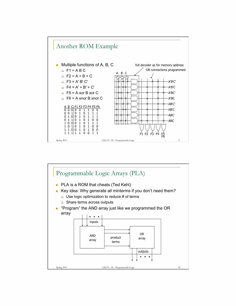
A B C F1 F2 F3 F4 F5 F6 0 0 0 0 0 1 1 0 0 0 0 1 0 1 0 1 1 1 0 1 0 0 1 0 1 1 1 0 1 1 0 1 0 1 0 0 1 0 0 0 1 0 1 1 1 1 0 1 0 1 0 1 0 0 1 1 0 0 1 0 1 0 0 1 1 1 1 1 0 0 1 1
A'B'C'
A'B'C
A'BC'
A'BC
AB'C'
AB'C
ABC'
ABC
A B C
F1 F2 F3 F4 F5 F6
full decoder as for memory address
OR connections programmed
Another ROM Example
Multiple functions of A, B, C F1 = A B C F2 = A + B + C F3 = A' B' C' F4 = A' + B' + C' F5 = A xor B xor C F6 = A xnor B xnor C
Spring 2010 CSE370 - IX - Programmable Logic 18
• • •
inputs
AND array
• • •
outputs
OR array product
terms
Programmable Logic Arrays (PLA)
PLA is a ROM that cheats (Ted Kehl) Key idea: Why generate all minterms if you don’t need them?
Use logic optimization to reduce # of terms Share terms across outputs
“Program” the AND array just like we programmed the OR array
Spring 2010 CSE370 - IX - Programmable Logic 19
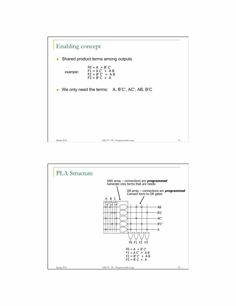
example: F0 = A + B' C' F1 = A C' + A B F2 = B' C' + A B F3 = B' C + A
Enabling concept
Shared product terms among outputs
We only need the terms: A, B’C’, AC’, AB, B’C
Spring 2010 CSE370 - IX - Programmable Logic 23
PLA Structure
AB
B'C
AC’
B’C’
A
A B C
F1 F2 F3 F0
AND array – connections are programmed Generate only terms that are needs
OR array – connections are programmed Connect term to OR gates
F0 = A + B' C' F1 = A C' + A B F2 = B' C' + A B F3 = B' C + A

Spring 2010 CSE370 - IX - Programmable Logic 24
example: F0 = A + B' C' F1 = A C' + A B F2 = B' C' + A B F3 = B' C + A
personality matrix 1 = uncomplemented in term 0 = complemented in term – = does not participate
1 = term connected to output 0 = no connection to output
input side:
output side:
product inputs outputs term A B C F0 F1 F2 F3 AB 1 1 – 0 1 1 0 B'C – 0 1 0 0 0 1 AC' 1 – 0 0 1 0 0 B'C' – 0 0 1 0 1 0 A 1 – – 1 0 0 1
reuse of terms
PLA Truth Table (Personality Matrix)
Shared product terms among outputs
Spring 2010 CSE370 - IX - Programmable Logic 25
PALs
Programmable array logic (PAL) Innovation by Monolithic Memories Programmable AND array Fixed OR array
faster and smaller OR plane No sharing of terms Limited number of terms per function
Spring 2010 CSE370 - IX - Programmable Logic 26
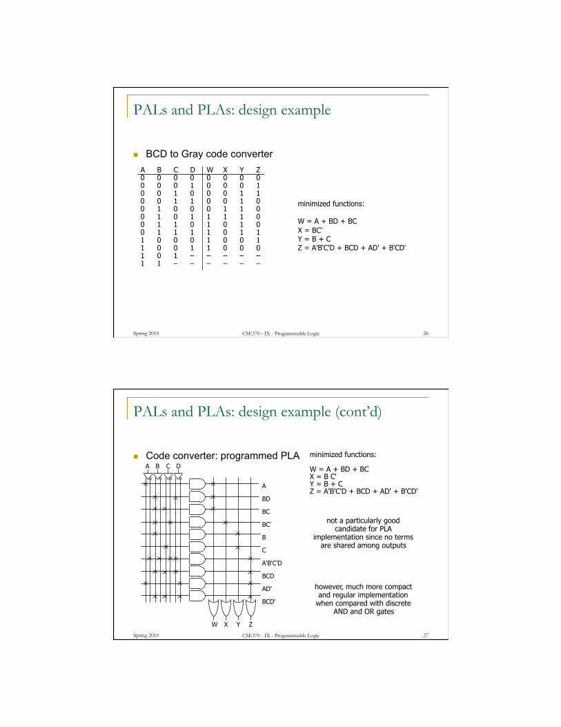
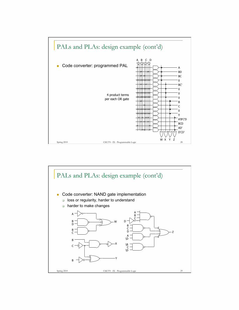
minimized functions:
W = A + BD + BC X = BC' Y = B + C Z = A'B'C'D + BCD + AD' + B'CD'
A B C D W X Y Z 0 0 0 0 0 0 0 0 0 0 0 1 0 0 0 1 0 0 1 0 0 0 1 1 0 0 1 1 0 0 1 0 0 1 0 0 0 1 1 0 0 1 0 1 1 1 1 0 0 1 1 0 1 0 1 0 0 1 1 1 1 0 1 1 1 0 0 0 1 0 0 1 1 0 0 1 1 0 0 0 1 0 1 – – – – – 1 1 – – – – – –
PALs and PLAs: design example
BCD to Gray code converter
PALs and PLAs: design example (cont’d)
Code converter: programmed PLA
Spring 2010 CSE370 - IX - Programmable Logic 27
not a particularly good candidate for PLA
implementation since no terms are shared among outputs
however, much more compact and regular implementation
when compared with discrete AND and OR gates
A B C D
minimized functions:
W = A + BD + BC X = B C' Y = B + C Z = A'B'C'D + BCD + AD' + B'CD'
A
BD
BC
BC'
B
C
A'B'C'D
BCD
AD'
BCD'
W X Y Z
Spring 2010 CSE370 - IX - Programmable Logic 28
4 product terms per each OR gate
A
BD
BC
0
BC'
0
0
0
B
C
0
0
A'B'C'D
BCD
AD'
B'CD'
W X Y Z
A B C D
PALs and PLAs: design example (cont’d)
Code converter: programmed PAL
Spring 2010 CSE370 - IX - Programmable Logic 29
W
X
Y
Z
B
B
B
B
B
B
\B C
C
C
C
C A
A A
D
D
D
\D
\D
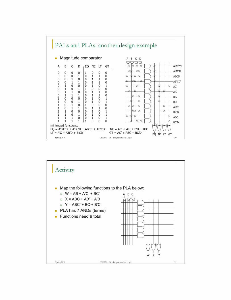
PALs and PLAs: design example (cont’d)
Code converter: NAND gate implementation loss or regularity, harder to understand harder to make changes
Spring 2010 CSE370 - IX - Programmable Logic 30 EQ NE LT GT
A'B'C'D'
A'BC'D
ABCD
AB'CD'
AC'
A'C
B'D
BD'
A'B'D
B'CD
ABC
BC'D'
A B C D
PALs and PLAs: another design example
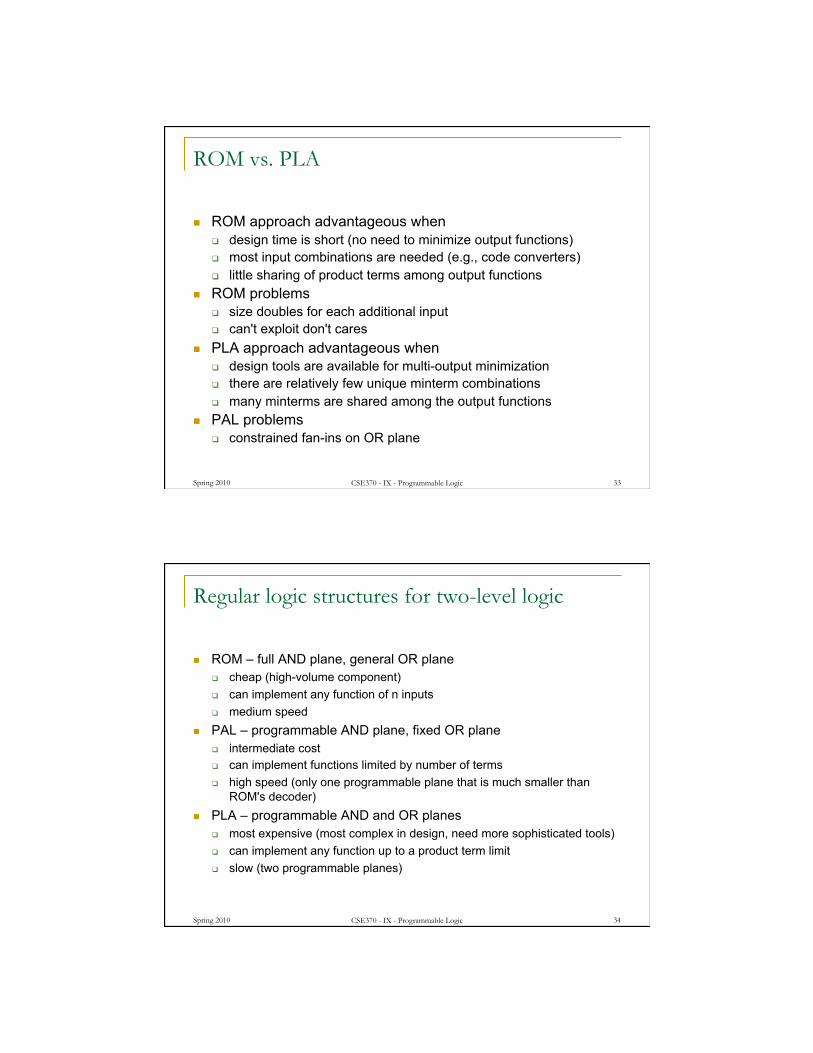
Magnitude comparator
A B C D EQ NE LT GT
0 0 0 0 1 0 0 0 0 0 0 1 0 1 1 0 0 0 1 0 0 1 1 0 0 0 1 1 0 1 1 0 0 1 0 0 0 1 0 1 0 1 0 1 1 0 0 0 0 1 1 0 0 1 1 0 0 1 1 1 0 1 1 0 1 0 0 0 0 1 0 1 1 0 0 1 0 1 0 1 1 0 1 0 1 0 0 0 1 0 1 1 0 1 1 0 1 1 0 0 0 1 0 1 1 1 0 1 0 1 0 1 1 1 1 0 0 1 0 1 1 1 1 1 1 0 0 0
minimized functions: EQ = A’B’C’D’ + A’BC’D + ABCD + AB’CD’ NE = AC’ + A’C + B’D + BD’ LT = A’C + A’B’D + B’CD GT = AC’ + ABC + BC’D’
Spring 2010 CSE370 - IX - Programmable Logic 31
Activity
Map the following functions to the PLA below: W = AB + A’C’ + BC’ X = ABC + AB’ + A’B Y = ABC’ + BC + B’C’
PLA has 7 ANDs (terms) Functions need 9 total
A B C
W X Y
Spring 2010 CSE370 - IX - Programmable Logic 33
ROM vs. PLA
ROM approach advantageous when design time is short (no need to minimize output functions) most input combinations are needed (e.g., code converters) little sharing of product terms among output functions
ROM problems size doubles for each additional input can't exploit don't cares
PLA approach advantageous when design tools are available for multi-output minimization there are relatively few unique minterm combinations many minterms are shared among the output functions
PAL problems constrained fan-ins on OR plane
Spring 2010 CSE370 - IX - Programmable Logic 34
Regular logic structures for two-level logic
ROM – full AND plane, general OR plane cheap (high-volume component) can implement any function of n inputs medium speed
PAL – programmable AND plane, fixed OR plane intermediate cost can implement functions limited by number of terms high speed (only one programmable plane that is much smaller than
ROM's decoder) PLA – programmable AND and OR planes
most expensive (most complex in design, need more sophisticated tools) can implement any function up to a product term limit slow (two programmable planes)
Spring 2010 CSE370 - IX - Programmable Logic 35
Regular logic structures for multi-level logic
Difficult to devise a regular structure for arbitrary connections between a large set of different types of gates efficiency/speed concerns for such a structure next we’ll learn about field programmable gate arrays (FPGAs)
that are just such programmable multi-level structures programmable multiplexers for wiring lookup tables for logic functions (programming fills in the table) multi-purpose cells (utilization is the big issue) much more about these in CSE467
Alternative to FPGAs: use multiple levels of PALs/PLAs/ROMs output intermediate result make it an input to be used in further logic no longer practical approach given prevalence of FPGAs
FPGAs in CSE370
Spring 2010 CSE370 - IX - Programmable Logic 36
http://www.altera.com/products/devices/cyclone2/overview/cy2-overview.html
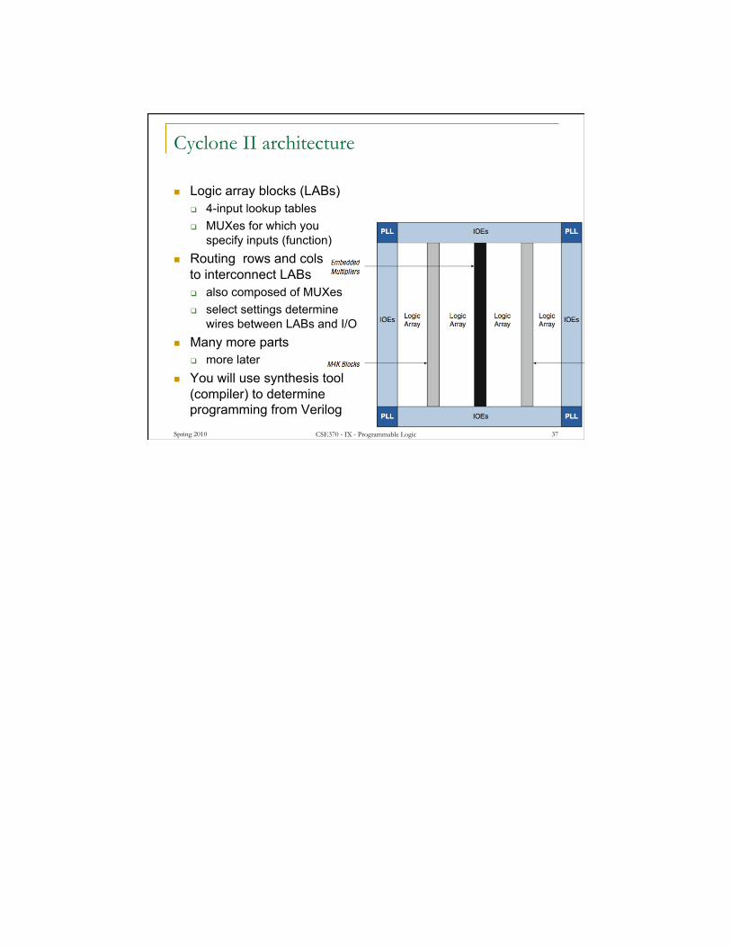
Cyclone II architecture
Logic array blocks (LABs) 4-input lookup tables MUXes for which you
specify inputs (function) Routing rows and cols
to interconnect LABs also composed of MUXes select settings determine
wires between LABs and I/O Many more parts
more later You will use synthesis tool
(compiler) to determine programming from Verilog
Spring 2010 CSE370 - IX - Programmable Logic 37