sprinkler buddy presentation #8: “testing/finalization of all modules and global placement”...
Post on 21-Dec-2015
215 views
TRANSCRIPT

Sprinkler Buddy
Presentation #8:
“Testing/Finalization of all
Modules and Global Placement”
3/26/2007
Team M3Kartik Murthy
Panchalam RamanujanSasidhar Uppuluri
Devesh Nema Kalyan Kommineni
Design Manager: Bowei Gai
“Low Cost Irrigation Management For Everyone ! ”
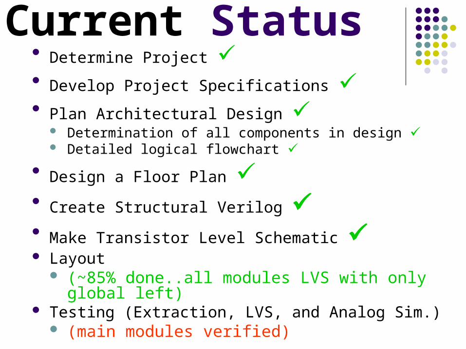
Current Status Determine Project Develop Project Specifications Plan Architectural Design
Determination of all components in design Detailed logical flowchart
Design a Floor Plan Create Structural Verilog Make Transistor Level Schematic Layout
(~85% done..all modules LVS with only global left) Testing (Extraction, LVS, and Analog Sim.)
(main modules verified)

Finalized Floor Plan

Transistor Count …
Block (# used) Old TC New TC
40:20 Muxes (6) 362 362
60:20 Muxes (2) 644 644
Counter (2) 220 220
KC ROM (1) 1256 1256
P ROM (1) 122 122
Metric Storage SRAMS (2)
2430 2430
Constant Storage ROM (1)
428 428
Floating Point Adder (4)
3210 3501Floating Point Multiplier (2)
1026 1026
10 Bit Registers (9)
210 210
Datapath Logic / Misc.
2305 2305
Total:
30,817

Updated Design SizeBlock (# used) Size (um)
40:20 Muxes (4) 20 x 80
60:20 Muxes (2) 20 x 120
Counter (2) 12 x 17
KC ROM (4 parts) 181 x 8
P ROM (1) 70 x 8
Metric Storage SRAMS (2)
181 x 60
Constant Storage ROM (1)
181 x 8
Floating Point Adder (4)
96x151
Floating Point Multiplier (2)
89 x 40
10 Bit Registers (8) 50 x 10
• 330um x 335 um• ~ 1 : 1.01 aspect ratio• .11 mm^2 area• .28 Density

Layout: Progress
All Big Modules LVS Global Wiring still has to be finished Control Logic locations estimated and
placed Needs wiring
Extracted Simulations Run on Major Blocks

Layout : 60-20 MUX
Density: .35 transistors/um2
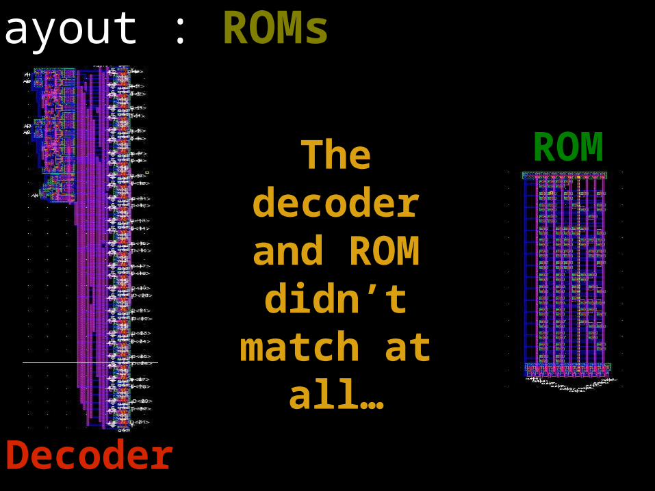
Layout : ROMs
The decoder
and ROM didn’t
match at all…
Decoder
ROM

Layout : ROMs
Changed Busses from M 1/2 to
3/4
Moved ROM under Bus

Layout : Shifter
Density: .35 transistors/um2

Layout : FP Add SIG Unit
Inputs
Density: .36 transistors/um2
Outputs

Layout : FP Add Exponent Unit
Density: .34 transistors/um2Outputs
Inputs

Layout : FP Adder FSM
Shaped to “Fill Gaps”

Layout : FP Adder
Density: .28 transistors/um2
Inputs
Outputs

Layout : Floating Point Multiply
Density: .34 transistors/um2
Inputs Outputs

Layout : Entire Chip
Density: .28 transistors/um2

Simulations : Extracted RC Mult
Clean Input
Input Through Min Sized Inv
1.175ns propagation delay
Multiplier Output

Simulations : Extracted RC Shifter
Output from Shifter
Output from Shifter
Clean Shift Signal
340ps propagation delay
Input Through Min Size Inv

Design Challenges and Implementation
DecisionsFor The Past Week
Design Challenge
Translation to HW
Avoiding “Black Space” in Layout
• Completed Global Level Layouts then shaped FSMs to fill gaps• Placed Entire Blocks under higher metal busses

Problems/QuestionsMetal Directionality is lost when we
rotate blocks Possible to ignore this in blocks we don’t
route over ? Especially bad in large blocks (FP Adder)
Even worse to correct

For Next TimeMore Layout
Global Routing Entire Chip Extracted RC Verification