sri final report draft3 - worcester polytechnic institute
TRANSCRIPT

AMISR SSPA
AUTOMATED TEST SUITE
Project Report
A Major Qualifying Project
submitted to the faculty of
WORCESTER POLYTECHNIC INSTITUTE
And performed at SRI INTERNATIONAL
in partial fulfillment of the requirements for the
Degree of Bachelor of Science
Date : March 2, 2007
WPI Advisor:
Professor John A. Orr
SRI Advisor:
Andrew Young
Submitted By:
Jeff Pelligrino John Scimone Kaushal Shrestha

ii
Table of Contents
Table of Contents ........................................................................................................................................... ii Table of Figures............................................................................................................................................. iv List of Tables...................................................................................................................................................v List of Tables...................................................................................................................................................v Abstract ......................................................................................................................................................... vi Executive Summary...................................................................................................................................... vii 1. Introduction........................................................................................................................................... 1 2. Background........................................................................................................................................... 2 2.1. National Science Foundation....................................................................................................... 3 2.2. Advanced Modular Incoherent Scatter Radar.............................................................................. 3
3. Project Goals......................................................................................................................................... 5 4. SSPA Design Specifications ................................................................................................................. 6 5. Technical Background .......................................................................................................................... 7 5.1. Phase 1: Calibration..................................................................................................................... 7 5.2. Phase 2: Pre Burn-in Test ............................................................................................................ 8 5.3. Phase 3: 24-hr Burn-in Test......................................................................................................... 8 5.4. Phase 4: Post Burn-in Test .......................................................................................................... 9 5.5. Phase 5: Design Verification Test ............................................................................................... 9
6. Automated Test Suite.......................................................................................................................... 11 6.1. System Design & Integration .................................................................................................... 13 6.1.1. Signal Generator .............................................................................................................. 15 6.1.2. Power Supply................................................................................................................... 15 6.1.3. RF Power Meter & Power Head ...................................................................................... 17 6.1.4. Switch Box....................................................................................................................... 19 6.1.5. Industrial PC .................................................................................................................... 20 6.1.6. Control Box...................................................................................................................... 23 6.1.7. Rack Design..................................................................................................................... 30
6.2. Platform..................................................................................................................................... 32 6.2.1. Hardware Architecture..................................................................................................... 32 6.2.2. Operating System............................................................................................................. 33 6.2.3. Programming Language................................................................................................... 34 6.2.4. Database Management System (DBMS) ......................................................................... 35
6.3. Software Architecture................................................................................................................ 36 6.3.1. Object Oriented Program Design..................................................................................... 37 6.3.2. Device level Abstraction.................................................................................................. 37 6.3.3. Device Interfacing............................................................................................................ 37 6.3.4. Class Modules.................................................................................................................. 40 6.3.5. Flow Control .................................................................................................................... 46 6.3.6. User Interface................................................................................................................... 52 6.3.7. Exceptions and Error Handling........................................................................................ 53 6.3.8. Database Programming and Data Storage........................................................................ 54
7. Twenty-Four Hour Burn-In System.................................................................................................... 58 7.1. System Requirement.................................................................................................................. 58 7.2. System Design........................................................................................................................... 58 7.3. Power Supplies .......................................................................................................................... 59 7.4. Loads ......................................................................................................................................... 59 7.5. Signal Sources ........................................................................................................................... 59 7.6. Signal Distribution System........................................................................................................ 60
8. Results................................................................................................................................................. 62 9. Conclusion .......................................................................................................................................... 63 References .................................................................................................................................................... 64 Appendix A ................................................................................................................................................ A-1

iii
Appendix B..................................................................................................................................................B-1 Appendix C..................................................................................................................................................C-1 Appendix D ................................................................................................................................................ D-1 Appendix E..................................................................................................................................................E-1

iv
Table of Figures
Figure 1: Artists concept of an AMISR radar with two faces......................................................................... 4 Figure 2: Block Diagram of Test System ..................................................................................................... 12 Figure 3: Test Station System Block Diagram ............................................................................................. 14 Figure 4: Agilent 5181A Signal Generator................................................................................................... 15 Figure 5: Agilent N6700A Power Supply .................................................................................................... 16 Figure 6: Agilent E4417A Power Meter and E9323A Power Heads............................................................ 18 Figure 7: Agilent 87106A Load Switch........................................................................................................ 19 Figure 8: National Instruments 488.2 GPIB Card ........................................................................................ 21 Figure 9: National Instruments PCI-6220 DAQ Card .................................................................................. 23 Figure 10: Input Stage Couplers................................................................................................................... 24 Figure 11: Output Stage Coupler.................................................................................................................. 25 Figure 12: Control Box System Diagram ..................................................................................................... 25 Figure 13: Control Box................................................................................................................................. 26 Figure 14: Front Panel of Control Box (Artist Concept) .............................................................................. 26 Figure 15: Front Panel of Control Box......................................................................................................... 26 Figure 16: Back Panel of Control Box (Artist Concept)............................................................................... 27 Figure 17: Back Panel of Control Box ......................................................................................................... 27 Figure 18. 7th order RF low pass filter.......................................................................................................... 28 Figure 19. S-parameters vs frequency .......................................................................................................... 29 Figure 20: Rack Layout ................................................................................................................................ 31 Figure 21: System Wiring Diagram.............................................................................................................. 32 Figure 22. Plot of Output Power Trace (dBm) vs. Time (ms) ...................................................................... 42 Figure 23. Plot of Output Power vs. number of samples over 2ms pulse ..................................................... 43 Figure 24. Plot of in-phase and quadrature-phase components of the phase of the RF output signal .......... 45 Figure 25. Plot of in-phase, quadrature-phase, pulse modulation signal and phase in radians..................... 46 Figure 26. Main Program Flow .................................................................................................................... 47 Figure 27: Calibration Process Flow ............................................................................................................ 48 Figure 28: Pre Burn-in Process Flow ........................................................................................................... 49 Figure 29: Post Burn-in Process Flow.......................................................................................................... 50 Figure 30: Power Meter Offset Calibration Flow........................................................................................ 51 Figure 31: Terminal based User Interface .................................................................................................... 52 Figure 32. Screenshot of the Manual Controls GUI ..................................................................................... 53

v
List of Tables
Table 1: Comparison of Signal Generators .................................................................................................. 15 Table 2: Comparison of Power Supplies ...................................................................................................... 16 Table 3: Power-meter specifications comparison......................................................................................... 17 Table 3: Power-head specifications comparison .......................................................................................... 18 Table 5: Load switch specification comparison ........................................................................................... 19 Table 5: Various industrial PC's and their respective specifications ............................................................ 20 Table 6: Comparison of different GPIB cards.............................................................................................. 21 Table 7: Comparison of different Digital I/O cards...................................................................................... 22 Table 8: Additional parts for the Digital IO cards ........................................................................................ 23 Table 9: Sample Calibration Data ................................................................................................................ 62 Table 10: Sample Pre Burn-in Data.............................................................................................................. 62

vi
Abstract
SRI International has been developing an Advanced Modular Incoherent Scatter
Radar (AMISR) for the purpose of observing upper-atmospheric phenomena with an
easily deployable modular radar system. This project was mostly concerned with the
power amplifier in the AMISR, specifically a Solid State Power Amplifier (SSPA). Our
project was to design and build an automated test station for use during production testing
and design verification testing as well as design circuitry that will be used during a
twenty-four hour burn-in test.

vii
Executive Summary
The National Science Foundation is funding the construction of a radar system to
be built in Alaska called AMISR, Advanced Modular Incoherent Scatter Radar. SRI
International, a non-profit research organization based in Menlo Park, California, is
responsible for the design and construction of the AMISR. The radar is unusual because
it is made up of a planar array of emitting elements. By controlling the phase
relationships between the elements, the radar beam can be instantaneously repositioned
without the use of mechanical systems. The AMISR project is slated to use 4,096 Solid
State Power Amplifiers (SSPAs). SRI is currently redesigning the amplifier and
production will be starting in the spring of 2007.
During production, each SSPA needs to be calibrated and tested to ensure that
each meets the specifications. Transporting equipment to the radar’s location is difficult
and costly because the deployment location for the AMISR is Poker Flats, Alaska. In
June of 2007, a barge will be departing for Alaska and all equipment for the AMISR must
be on board or else it will delay the project for another year. Since this does not leave
much time for the production and testing of the SSPAs, SRI needs an automated test
station that is capable of calibrating and performing a specification test on an amplifier in
five minutes without unnecessary human interaction. The test station must be simple to
use, self-calibrating, portable, and able to store test data in an easily accessible database.
After the initial calibration, each unit will be tested to ensure it meets the
specifications set forth by SRI. These tests include power measurements at multiple
frequencies, amplifier efficiency measurements, and an input power variation test. In
order to conduct all required tests, an integrated system needed to be built. The system
became known as the Automated Test Suite (ATS). It required the implementation of a
power supply, signal generator, power meter, I/Q detector, and a computer to control the
test equipment as well as provide the user interface.
A control box had to be designed to provide a signal control center for interfacing
multiple devices. The control box distributes the timing signals generated by the

viii
computer’s data acquisition card (DAQ) to various components. It also interfaces the I/Q
detector with the analog inputs of the DAQ, contains the directional couplers and
attenuators that are needed to make power measurements, as well as the switch that
changes the load that is connected to the SSPA.
The I/Q detector consists of Analog Device’s AD8347 demodulator chip
implemented using its evaluation board. The I/Q detector demodulates the in-phase and
quadrature phase components of a signal by mixing a reference signal with the output RF
signal. When the two signals are mixed, the output’s frequency domain has peaks at DC
and 880MHz. Since the DC signal is the one that represents the phase of the SSPA, we
designed an RF filter to eliminate the 880MHz signal. The I/Q Detector was also
modified to disable the automatic voltage offset compensation feature.
A significant amount of time was spent developing code to intelligently calibrate
and test the amplifiers without any human intervention because the station needed to be
automated. Several software-related obstacles needed to be overcome during the project.
The drivers for the DAQ card and the GPIB card had to be installed on Linux without
manufacturer support. In addition, interfacing Python with the GPIB card and DAQ card
was difficult because Python was an unfamiliar language. A Python package called
PyVISA, which is a wrapper for National Instrument’s GPIB control libraries, was used
to inteface the GPIB card. For the DAQ card, a custom wrapper was written in C to
interface the Python code with the hardware because there were no preexisting wrappers.
After overcoming these difficulties, all that remained was the task of writing the software
to drive the system and store measurements and results into a database.
We undertook the additional responsibility of designing and developing the burn-
in system because the original project was ahead of schedule. The burn-in system is
required to run ninety-six amplifiers for a twenty-four hour period. During this time, the
SSPAs need to be monitored to make sure they are on for the full length of the test. The
burn-in process tests the units for component failures prior to installing the amplifiers in
the field. A single signal generator is used to supply the necessary RF input signal for
operating all ninety-six amplifiers concurrently. The burn-in system is designed in two

ix
stages. The first stage splits the input RF and timing signals six ways while the second
stage splits each output from stage-one sixteen ways. To make operation of the burn-in
system easier for the user, stage-two had to be designed with latching circuitry to indicate
if an SSPA’s alarm signals tripped during the test. As an added feature, there is also an
indicator to show when an amplifier has been tested for twenty-four hours. A circuit
board was designed to meet the requirements of the second stage of the burn-in system.
Revision one was fabricated, populated, and troubleshot with modifications made to
demonstrate the required changes for revision two. The modifications were replicated in
the schematics and the revised design has been submitted for layout changes.
The Automated Test Suite project has been successfully completed. The station is
physically complete and the software has been fully implemented. Since production of
the SSPAs has not started, new production tests are being developed and the DVT test
suite may be altered in the future. The burn-in system, which was assigned as a secondary
project, is not yet complete. Stage-one has been tested and is complete, however, the
stage-two circuit board has entering its second revision and will be completed by the
staffs at SRI International..

1
1. Introduction
SRI International, a non-profit research and development organization, is in the
process of developing an Advanced Modular Incoherent Scatter Radar (AMISR) for the
purpose of observing upper-atmospheric phenomena with an easily deployable modular
radar system. The AMISR uses phased scanning principles allowing quick redirection of
the scanning lobe without any physical movements of the antenna elements. The AMISR
consists of antennas, power amplifiers, low noise amplifiers, delay shifting circuitry,
control circuitry, a power supply system, and a chassis to hold the equipment together.
The power amplifier in the antenna element unit (AEU), specifically a Solid State Power
Amplifier (SSPA), is what this project was mostly concerned with because the SSPA is
being redesigned and the units will need to be tested to ensure their proper functionality.
Our project was to design and build an automated test station for this purpose as well as
design circuitry that will be used during a twenty-four hour burn-in test.

2
2. Background
Founded in 1946 by a group of west coast industrialists and Stanford University,
SRI remains a research institution committed to the discovery and application of new
technology in fields ranging from communications to the biomedical industry. In 1970
SRI separated from Stanford University and in 1977 formally changed its name from
Stanford Research Institute to SRI International. The company holds more than 1,000
patents worldwide. There are currently over 1,400 people employed by SRI International
alone. In addition, over 600 people are employed at its subsidiary Sarnoff Corporation.
Their main offices are located in Menlo Park, CA however they have additional offices
located in Washington, DC and Tokyo, Japan as well as several other US locations.
In an effort to move technology developed at SRI to the marketplace, SRI
international has worked in conjunction with their subsidiary Sarnoff Corporation and
top-tier investment and venture capital firms to form approximately two dozen new
ventures. These ventures include companies such as Artificial Muscle Inc, Bridge
Pharmaceuticals, Spanlink Communications, and Intuitive Surgical Inc. Sarnoff
Corporation has won 10 Emmy awards and developed the HDTV standard used in the US.
SRI has also won an Academy award and is recognized for developing the current
automated check processing system that utilizes magnetic ink coding, the world’s first
computer network which was known as ARPANET, and the first prototype of a computer
mouse.
SRI International is expanding rapidly. They were recently awarded $56.9 million
from the National Institute of Allergy and Infectious Diseases for research and
development of drugs and antibodies for anti-infective therapeutics. SRI International is
also opening a new research facility in St. Petersburg, FL for marine technology research.
The facility will research and develop technologies related to ocean science, the maritime
industry, and port security.

3
2.1. National Science Foundation
In 1950, congress created the National Science Foundation, an independent
federal agency, to encourage the advancement of science, national health and prosperity,
and to improve national security. The government’s reliance on innovation and scientific
progress intensified during the World War II. Following the war, government
involvement in universities and science was at an all-time high. At this time, several
congressmen and scientists pushed for legislature to create an agency to fund scientific
research through government grants, this agency became known as the National Science
Foundation (NSF).
Today, the NSF is the funding source for approximately twenty percent of all
federally sponsored university research. The agency also funds high-risk, high-payoff
ideas that are on the bleeding edge of innovation. An example from the National Science
Foundation’s website is nanotechnology. They were funding scientists who were
researching ways to manipulate movement on an atomic level, years before the public
had even heard of nanotechnology.
In addition to funding research, the NSF also helps finance high-cost equipment
and facilities that are too expensive for one research group or researcher. This includes
“giant optical and radar telescopes, Antarctic research sites, high-end computer facilities
and ultra-high-speed connections, ships for ocean research, sensitive detectors of very
subtle physical phenomena and gravitational wave observatories.” One of the projects
that the NSF has funded for the past 10 years is the AMISR project.
2.2. Advanced Modular Incoherent Scatter Radar
The Advanced Modular Incoherent Scatter Radar, AMISR, is a mobile radar
facility that will eventually be utilized by scientists to study the atmosphere and observe
space weather events. The project is funded by the National Science Foundation and is
being developed in a collaborative effort led by SRI International. SRI is responsible for

4
the lead design and construction of the radar as well as overseeing operations and the
initial design verification tests. Sanmina-SCI and VECO Alaska are manufacturing the
antenna element units and overseeing the structural engineering of the radar respectively.
This radar will be built using a phased-array antenna system that will allow the radar to
function in different configurations. The system will be controlled remotely and the radar
beam will be electronically controlled allowing scientists to instantaneously position the
beam to accurately measure changing weather events. The AMISR utilizes three separate
radar faces, each consisting of 128 panels, which can be deployed in up to three separate
locations. In Figure 1, the AMISR radar is pictured with two full faces. The first radar
face is being constructed in Poker Flat, Alaska and subsequent faces will be constructed
in Resolute Bay, Canada, and Nunavut, Canada. Each face of the radar is made up of 8
groups of panels. Each group has 16 panels and therefore each face has 128 panels. There
can be up to 32 solid state power amplifiers (SSPA) per panel. Therefore, each face can
have up to 4,096 individual transmit and receive elements.
Figure 1: Artists concept of an AMISR radar with two faces.

5
3. Project Goals
The goal of this project was to design and build an automated test station for the
SSPA. The test station should be able to calibrate the amplifier, and then test the RF
characteristics of the unit such as power gain, current draw, amplitude, phase, and VSWR
at the upper and lower signal frequency limits as well as the middle operating frequency.
Following the RF characteristic tests, the test station will check the fault conditions of the
amplifier, such as an open output, and a mismatched load. The automated test station
must also be capable of powering an SSPA during environmental testing, including
periodic measurements of power, current, ambient temperature, and device temperature.
The automated test system must be capable of testing the RF characteristics of
about 1000 SSPAs per month at the rate of about forty per day. Testing will be conducted
twenty-three days per month and testing will take place during an eight hour shift on
these days. The expected yield rate is approximately 90% based on information provided
by SRI and therefore we will be designing our test system to test each SSPA in less than
five minutes. For the twenty-four hour burn-in process, which will not utilize the ATS,
our goal was to design a system to test multiple SSPAs during a single twenty-four hour
period.

6
4. SSPA Design Specifications
The SSPAs are designed to meet a number of important specifications. The
Automated Test Suite is designed to test these specifications to ensure that each SSPA
meets the designated requirements. The requirements include:
Full Operating Temperature:
• -40 Degrees C to 35 Degrees C
RF Power:
• Input: 10dBm ± 1.5dB
• Output: 57dBm (-0/+.5dB)
RF Pulse Characteristics:
• Minimum Pulse Width: 1µs
• Maximum Pulse Width: 2ms
• Amplitude Droop: <10% at maximum pulse width
Phase Response:
• Unit-to-Unit match: ± 5 degrees
Stability/Impedance:
• Input VSWR : < 1.3:1
• Output VSWR : < 1.5:1
Protection:
• Over-drive protection if input exceeds specified range
• VSWR mismatch protection when VSWR is greater that 6:1
• Over-temperature protection
Each SSPA will also be subjected to a twenty-four hour burn-in test that will not
utilize the ATS. After the burn-in procedure, each SSPA will be retested on the ATS to
ensure that it is still functioning properly.

7
5. Technical Background
When a company produces a device in large quantities, it is important to ensure
that each product meets the company’s standards. Production testing allows companies to
determine if a device meets its requirements before the device is sold or delivered. SRI
needs to conduct production testing on the SSPA’s to ensure that they meet their
specifications. Test data from production testing provides many useful statistics to
companies like SRI. Test data allows companies to determine if there are reoccurring
problems or manufacturing trends that could potentially affect future products. There are
five phases of testing for the AMISR SSPAs.
• Phase 1: Calibration
• Phase 2: Pre Burn-in Test
• Phase 3: 24-hr Burn-in Test
• Phase 4: Post Burn-in Test
• Phase 5: Design Verification Test
Four phases involve the ATS; they include calibration, pre burn-in testing, post
burn-in testing, and the design verification testing. The third phase, the twenty-four hour
burn-in process, does not utilize the ATS, however, it utilizes the burn-in distribution
system which will be discussed later in this report. It is important to note that only the
first four phases are included in production testing. The design verification testing (DVT)
will not be performed on every SSPA; only select number of amplifiers will be subjected
to DVT.
5.1. Phase 1: Calibration
Phase 1 of production testing is used to calibrate each SSPA prior to design
specification testing. During calibration, the VSWR, output power, and phase of each
SSPA is calibrated and set to ensure proper matching between SSPAs. A list of steps for
the automated calibration phase can be found below.
• Initialize Devices

8
• Initialize Digital Potentiometers
• Set Driver Bias
• Set Output Bias
• Set Gain
• Set Phase
• Set VSWR
5.2. Phase 2: Pre Burn-in Test
After the calibration procedure, pre burn-in testing is conducted to further verify
the device meets the design requirements. There are five tests performed during pre burn-
in testing. The output power and current are verified at three frequencies at the beginning
of the test. An over pulse width test is conducted to verify that each SSPA automatically
limits the pulse width to less than 2.5ms when the pulse width is outside its specifications.
The fifth test verifies that the amplifier gain is consistent when the input is decreased to
8.5dBm and increased to 11.5dBm. The various tests for pre burn-in are listed below.
• Output Power & Current Verification: 440MHz
• Output Power & Current Verification: 430MHz
• Output Power & Current Verification: 450MHz
• Over Pulse Width Test
• Input Power Variation Test
• Efficiency Test
• Open Circuit Test
• VSWR 3:1 Trip Test
5.3. Phase 3: 24-hr Burn-in Test
The next phase is the twenty-four hour burn-in test which consists of running
ninety-six SSPAs at once while monitoring the two status bits—over-temperature and
VSWR fault. Each amplifier that passes the twenty-four hour burn-in process is retested
during post burn-in testing. The twenty-four hour burn-in test utilizes the distribution
board that was designed to simplify the wiring of the system, monitor the two status bits,
and to alert a user when each SSPA has run for the full twenty-four hours.

9
5.4. Phase 4: Post Burn-in Test
During phase 4 of production testing, the same tests that were completed during
phase 2 will be completed again. This will allow engineers to determine if the twenty four
hour burn-in test affected the performance characteristics of each SSPA. The various tests
for post burn-in are listed below.
• Output Power & Current Verification: 440MHz
• Output Power & Current Verification: 430MHz
• Output Power & Current Verification: 450MHz
• Over Pulse Width Test
• Input Power Variation Test
• Efficiency Test
• Open Circuit Test
• VSWR 3:1 Trip Test
5.5. Phase 5: Design Verification Test
One out of every sixty-four SSPAs will be subjected to design verification testing.
The design verification test package in the ATS system includes a qualification test, pre-
environmental test benchmark, post-environmental test benchmark, and an operating test.
The design verification test plan entails an initial qualification test and then a series of
environmental tests. DVT includes many environmental tests, some environmental tests
will be conducted when the amplifier is operation and others will be conducted when the
amplifier is in non-operational mode. The operating test will be used to collect data
during environmental tests that include an operating amplifier. The pre-environmental
test will be conducted before an amplifier is subjected to a non-operational environmental
test and a post-environmental test will be conducted after a non-operational
environmental test. The design verification test plan is shown below.
Qualification Test: (Performed at 430, 440, and 450MHz for each SSPA)
• Power Consumption (Input Current and Input Voltage)
• RF Power Output
• Amplifier Gain
• RF Pulse Droop (2ms Pulse Width)
• Amplifier Insertion Phase

10
Environmental Tests:
• Low & high temperature stress testing (SSPA Operational).
• Random vibration stress testing (SSPA Operational).
• Temperature Cycling with & without vibration step (SSPA Operational)
• Temperature Cycling with Condensation (SSPA non-operational)
• Random Vibration (SSPA non-operational)
• Half sine shock test (SSPA non-operational)
• Low Temperature Soak Test – 22hr duration (SSPA operational)
• High Temperature Soak Test – 22hr duration (SSPA operational)
• Temperature Cycling without Condensation – 48hr duration (SSPA operational)
• Humidity Cycling without Condensation – 96hr duration (SSPA operational)

11
6. Automated Test Suite
The automated test suite (ATS) was designed to simplify the testing of the SSPAs.
The ATS in used in the following phases of production testing:
• Calibration
• Pre Burn-in Testing
• Post Burn-in Testing
• Design Verification Testing
The ATS has been designed to meet several specifications. These specifications
are listed below.
• Conduct Calibration and Pre Burn-in Test in less than 5 minutes.
• Must be capable of measuring phase, power, and current.
• ATS must be capable of being relocated easily.
• Easy to modify calibration tolerances.
• System must be self-calibrating.
• System must be network accessible.
• Data must be stored in a database.
• Data must be easily accessible.
• Simple to use.
The block diagram shown in Figure 2 summarizes the test system setup.

12
500W peak / 50W avg Switch
Ethernet
Power Sensor
E9323A
Power Sensor
E9323A
Local Oscillator
for IQ Detector
Ethernet
Figure 2: Block Diagram of Test System

13
6.1. System Design & Integration
The ATS includes a number of major components, all of which are integrated
within our stand alone system. These include:
• Industrial PC
• RF power meter and power heads
• Power supply
• GPIB card
• Digital I/O card
• Signal generator
• Control Box
• Switch Box
The system diagram in Figure 3 shows how these different resources are
connected and implemented. As you can see in the diagram, the industrial PC controls the
test station. It communicates with various components through GPIB, Ethernet, and
through the digital I/Os of the DAQ. The components that are controlled by the PC
include the power supply, power meter, signal generators, and DAQ card. Each of these
components connect to the SSPA, with the exception of the power meter which connects
to the SSPA via the power heads. A switch box is also connected to the output of the
SSPA and is used to switch between various loads.

14
Industrial PC
Power
Meter
Signal
Generator
SSPA
Power
Supply
DAQGPIB
Power
Heads
Ethernet
Switch
BoxLoads
Figure 3: Test Station System Block Diagram

15
6.1.1. Signal Generator
The signal generator is used to produce our test signal. The frequency that the RF
amplifiers will operate, between 430 MHz and 450 MHz, is within the limits of many of
the signal generators we found which are shown in Table 1. It is important that the signal
generator is programmable because we need to control it using our industrial PC. The
Agilent N9310A signal generator was chosen because of its short lead-time, low-cost,
and it is programmable via ethernet.
Company Model # Price Lead Time
Programmable Pulse Modulation Built-in
Agilent E4400B ESG-A
$8,162 8 weeks N/A N/A
Agilent N9310A $6,810 4 weeks Yes Yes
Agilent N5181A $6,349 4 Weeks Yes Yes Table 1: Comparison of Signal Generators
Figure 4: Agilent 5181A Signal Generator
6.1.2. Power Supply
The DC power supply is an important component of the test station. The power
supply must be capable of covering the operating voltage and current ranges and must be
able to be programmed remotely to allow automation of the testing procedure. This
means that there must be a USB, Ethernet, or GPIB interface for programming. During
the calibration and normal operation of the SSPA, the supply voltage needs to be 32V.
Another important feature for the power supply is the current sensing resolution. The
power supply must be able to supply 5A maximum current and should have a high
16
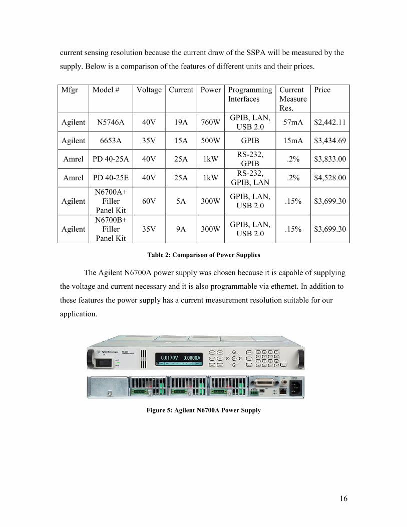
current sensing resolution because the current draw of the SSPA will be measured by the
supply. Below is a comparison of the features of different units and their prices.
Mfgr Model # Voltage Current Power Programming Interfaces
Current Measure Res.
Price
Agilent N5746A 40V 19A 760W GPIB, LAN, USB 2.0
57mA $2,442.11
Agilent 6653A 35V 15A 500W GPIB 15mA $3,434.69
Amrel PD 40-25A 40V 25A 1kW RS-232, GPIB
.2% $3,833.00
Amrel PD 40-25E 40V 25A 1kW RS-232,
GPIB, LAN .2% $4,528.00
Agilent N6700A+ Filler
Panel Kit 60V 5A 300W
GPIB, LAN, USB 2.0
.15% $3,699.30
Agilent N6700B+ Filler
Panel Kit 35V 9A 300W
GPIB, LAN, USB 2.0
.15% $3,699.30
Table 2: Comparison of Power Supplies
The Agilent N6700A power supply was chosen because it is capable of supplying
the voltage and current necessary and it is also programmable via ethernet. In addition to
these features the power supply has a current measurement resolution suitable for our
application.
Figure 5: Agilent N6700A Power Supply

17
6.1.3. RF Power Meter & Power Head
We require RF Power-meters to be able to measure the input power into and the
output power out of the power amplifier. The output power of the amplifier is expected to
be approximately 500W of peak power or +57dBm. It is not easy to measure very high
power directly; hence we will have to go through the process of attenuation before power
measurements. Some of the specifications that we are looking in terms of power-meters
and power-heads are:
• High sampling rate
• Peak power measurement capability
• High video bandwidth
• Wide power measurement range We needed a high sampling rate because we need to perform a droop test. This
involves capturing a trace of the output power and measuring the droop associated with
the pulse. The peak power measurement capability is required because the RF pulse is
only of 10% duty cycle which can output a maximum of 500W power or 50W average
power. The high video bandwidth is required to measure sharp rising edge triggers. The
wide power measurement range is an optional specification for flexibility. The tables
below (Table 3 and Table 4) summarize the various power meter products and power-
head products that are able to fulfill our technical requirements.
Table 3: Power-meter specifications comparison
Manufacturer Model Measurement Sampling rate /Measurement rate
Bandwidth Price US$
Agilent E4417A Peak, Average, Peak-to-average ratio
20 Msample/s 7,077
Agilent N1912A Peak, average, Peak-to-average ratio, rise time, fall time and pulse width
100 Msample/s 50 MHz to 40 GHz
10,214
Gigatronics 8540C Peak, average and CW 500-4000 reading/s
100 kHz to 40 GHz
N/A
Gigatronics 8502A peak power, time, fall time and pulse width plus
70 measurements of a point/second
.03 or 0.75 to 18.5, 26.5 or 40 GHz
N/A

18
Manufacturer Series Product Frequency Range
Power Range Video BW Price from (US$)
Agilent E9320 E9321A 50 MHz to 6 GHz
-65 dBm (320 pW) to +20 dBm (100 mW)
300 kHz 1,567
Agilent E9322A E9322A 50 MHz to 6 GHz
-60 dBm (1nW) to +20 dBm (100 mW)
1.5 MHz 2,089
Agilent E9323A E9323A 50 MHz to 6 GHz
-60 dBm (1 nW) to +20 dBm (100 mW)
5 MHz 2,867
Agilent E9325A E9325A 50 MHz to 18 GHz
-60 dBm (320 pW) to +20 dBm (100 mW)
300 kHz 1,880
Agilent E9326A E9326A 50 MHz to 18 GHz
-60 dBm (1 nW) to +20 dBm (100 mW)
1.5 MHz 2,507
Agilent E9327A E9327A 50 MHz to 18 GHz
-60 dBm (1 nW) to +20 dBm (100 mW)
5 MHz 3,336
Agilent N192XA N1921A 50 MHz to 18 GHz
-35 dBm to +20 dBm N/A 3,763
Gigatronics 200mW PPS
80350A 45 MHz to 18 GHz
-20 to +20 dBm / +23dBm
N/A N/A
Gigatronics 5 W PPS 80351A 45 MHz to 18 GHz
0 to +40 dBm / +43 dBm
N/A N/A
Gigatronics 25 W PPS
80352A 45 MHz to 18 GHz
+10 dBm to +50 dBm / +53 dBm
N/A N/A
Gigatronics 50 W PPS
80355A 45 MHz to 18 GHz
+10 to +50 dBm / +53 dBm
N/A N/A
Table 4: Power-head specifications comparison
For the power-meter, Agilent E4417A was chosen because it met all of our
specifications along with our budget. For the power-head, the Agilent E9323A was
chosen over other Agilent E-series primarily because if it’s high video bandwidth
specification.
Figure 6: Agilent E4417A Power Meter and E9323A Power Heads

19
6.1.4. Switch Box
The switch box must be a single pole five throw switch cable of handling 50W
average input power and 500W peak input power. A VSWR as close to 1 as possible is
desirable so that the loads following the switch are properly matched to the amplifier
under test. The switch must also be programmable so that the computer can control the
load configuration and automate the test plan.
Manufacturer and Part Number
Frequency range
Insertion Loss Isolation SWR Connectors Control Logic
Agilent 87106A DC to 4GHz
0.3dB + .015 x Freq.(GHz)
100dB Min
1.2 Max
SMA Internal Control Logic
Agilent 87106B DC to 20GHz
0.3dB + .015 x Freq.(GHz)
70dB Min
1.7 Max
SMA Internal Control Logic
Agilent 87206B DC to 4GHz
0.3dB + .015 x Freq.(GHz)
100dB Min
1.2 Max
SMA Requeires External Control Logic
Table 5: Load switch specification comparison
The Agilent 87106A switch was chosen because it meets the necessary
requirements. The switch also provides flexibility for future adjustments to the ATS
because it is a six-pole switch.
Figure 7: Agilent 87106A Load Switch
20
6.1.5. Industrial PC
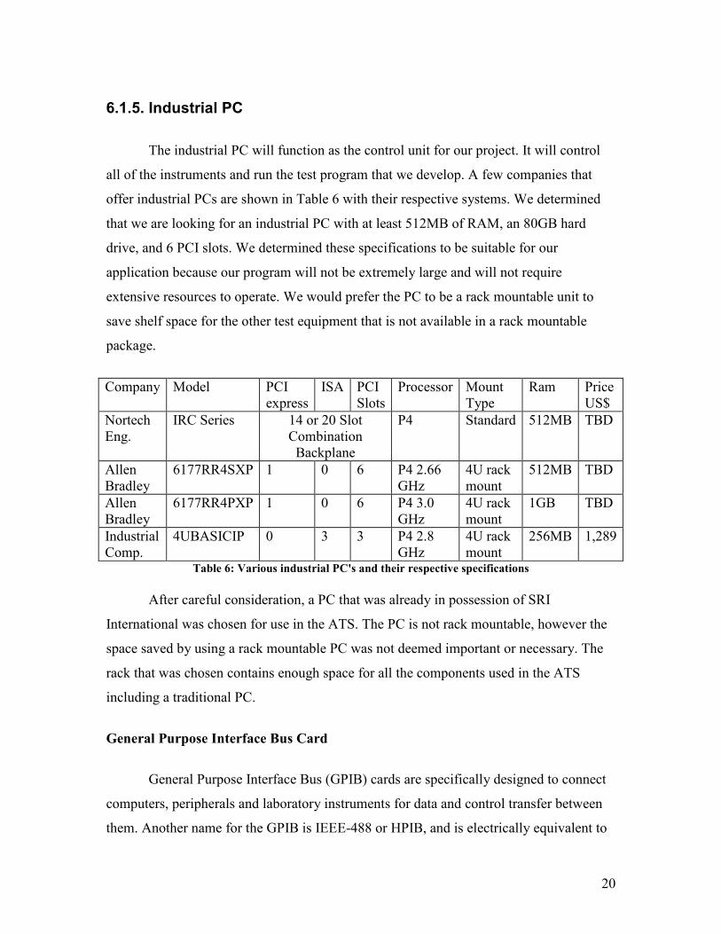
The industrial PC will function as the control unit for our project. It will control
all of the instruments and run the test program that we develop. A few companies that
offer industrial PCs are shown in Table 6 with their respective systems. We determined
that we are looking for an industrial PC with at least 512MB of RAM, an 80GB hard
drive, and 6 PCI slots. We determined these specifications to be suitable for our
application because our program will not be extremely large and will not require
extensive resources to operate. We would prefer the PC to be a rack mountable unit to
save shelf space for the other test equipment that is not available in a rack mountable
package.
Company Model PCI express
ISA PCI Slots
Processor Mount Type
Ram Price US$
Nortech Eng.
IRC Series 14 or 20 Slot Combination Backplane
P4 Standard 512MB TBD
Allen Bradley
6177RR4SXP 1 0 6 P4 2.66 GHz
4U rack mount
512MB TBD
Allen Bradley
6177RR4PXP 1 0 6 P4 3.0 GHz
4U rack mount
1GB TBD
Industrial Comp.
4UBASICIP 0 3 3 P4 2.8 GHz
4U rack mount
256MB 1,289
Table 6: Various industrial PC's and their respective specifications
After careful consideration, a PC that was already in possession of SRI
International was chosen for use in the ATS. The PC is not rack mountable, however the
space saved by using a rack mountable PC was not deemed important or necessary. The
rack that was chosen contains enough space for all the components used in the ATS
including a traditional PC.
General Purpose Interface Bus Card
General Purpose Interface Bus (GPIB) cards are specifically designed to connect
computers, peripherals and laboratory instruments for data and control transfer between
them. Another name for the GPIB is IEEE-488 or HPIB, and is electrically equivalent to

21
IEC-625 bus. GPIB uses 16 line parallel connections which are divided into eight data
lines, three handshake lines for synchronous transfer and five management lines to
control the bus. To use the GPIB, we need a GPIB adaptor card in the computer and a
GPIB cable. The GPIB cards generally go into the PCI slot of the computer which will be
used to control the automated test unit. The GPIB will be used to communicate with the
power meter and feed the measurement readings back into our program. There are a
variety of GPIB cards with different specifications which are summarized in Table 7.
Manufacturer Part Number Specifications / Comments Price US$
National Instruments
778032-01 NI PCI-GPIB NI-488.2 for Windows 2000/XP (Includes Type X2 Cable, 2M)
529.00
National Instruments
778032-51 PCI-GPIB NI-488.2 for Windows 2000/XP (Includes Type X2 Cable, 2M)
599.00
National Instruments
778686-01 PCI-GPIB NI-488.2 for LINUX (Includes Type X2 Cable, 2M)
529.00
National Instruments
778686-51 PCI-GPIB NI-488.2 for LINUX (Includes Type X2 Cable, 2M)
599.00
Table 7: Comparison of different GPIB cards
The GPIB card from National Instrument, NI PCI-GPIB NI-488.2 for Linux w/ 2
meter cable, part number 778686-51, was chosen because it fits into our budget easily
and National Instruments provides extensive technical support. The fact that the GPIB
card specifically says for Linux systems ensures us that there are some drivers and
support for Linux.
Figure 8: National Instruments 488.2 GPIB Card
22
Data Acquisition Card (DAQ)
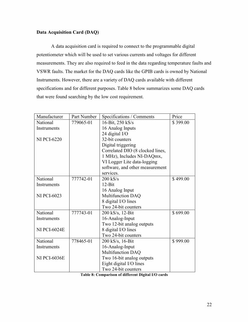
A data acquisition card is required to connect to the programmable digital
potentiometer which will be used to set various currents and voltages for different
measurements. They are also required to feed in the data regarding temperature faults and
VSWR faults. The market for the DAQ cards like the GPIB cards is owned by National
Instruments. However, there are a variety of DAQ cards available with different
specifications and for different purposes. Table 8 below summarizes some DAQ cards
that were found searching by the low cost requirement.
Manufacturer Part Number Specifications / Comments Price
National Instruments NI PCI-6220
779065-01 16-Bit, 250 kS/s 16 Analog Inputs 24 digital I/O 32-bit counters Digital triggering Correlated DIO (8 clocked lines, 1 MHz), Includes NI-DAQmx, VI Logger Lite data-logging software, and other measurement services.
$ 399.00
National Instruments NI PCI-6023
777742-01 200 kS/s 12-Bit 16 Analog Input Multifunction DAQ 8 digital I/O lines Two 24-bit counters
$ 499.00
National Instruments NI PCI-6024E
777743-01 200 kS/s, 12-Bit 16-Analog-Input Two 12-bit analog outputs 8 digital I/O lines Two 24-bit counters
$ 699.00
National Instruments NI PCI-6036E
778465-01 200 kS/s, 16-Bit 16-Analog-Input Multifunction DAQ Two 16-bit analog outputs Eight digital I/O lines Two 24-bit counters
$ 999.00
Table 8: Comparison of different Digital I/O cards

23
Each NI PCI-6XXX series requires: 1 Cable, 1 Connector Block. The part
numbers are different depending on which IO card is chosen, however the prices are the
same as shown in Table 9.
Manufacturer Part Specifications / Comments Price
National Instruments Cable SH68-68-EP Cable (2m) $ 119
National Instruments Connector Block SCC-68 -Unshielded $ 299 Table 9: Additional parts for the Digital IO cards
Digital IO card from National Instruments, NI PCI-6220, part number 779065-01,
was chosen because of its low cost, and sampling rate of 250kS/s. The number of analog
inputs and digital outputs (16 and 24 respectively) is suitable for our application.
Figure 9: National Instruments PCI-6220 DAQ Card
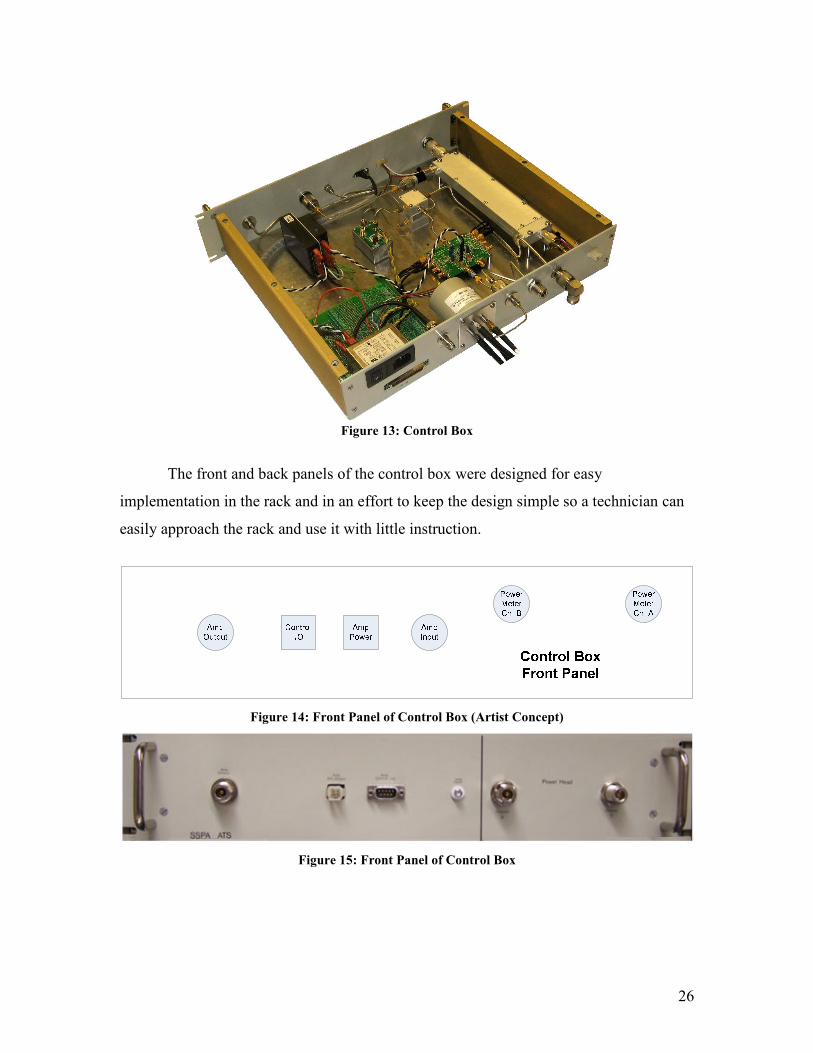
6.1.6. Control Box
The control box was built in an effort to simplify the wiring and installation of the
devices in the Automated Test Suite. The ATS requires a large number of connections to
be made between devices and the control box was designed to make this easier for both
the original designers as well as test and service technicians. The following devices are
contained within or interfaced using the control box:

24
• Signal Generator
• Power Supply
• Power Heads
• Data Acquisition Card
• Load Switch
• Five Loads
• I/Q Detector
• Pulse Modulation Switch
• Three Couplers
• One Attenuator
The control box design allows the SSPA input, output, controller, and power to
plug into the front of the control box, while the remaining connections are made in the
rear of the box. The couplers and attenuator are incorporated into the control box to
ensure they are never accidentally removed because that could permanently damage the
power heads. The RF input amplitude is 10dBm and the signal passes through two 20dB
couplers that are implemented in series as shown below. The first input coupler attenuates
the signal to approximately -10dB and provides the LO signal for the I/Q detector. The
second input coupler also attenuates the signal to -10dBm prior to being measured by the
power meter using channel A.
Figure 10: Input Stage Couplers
The output stage of the control box utilizes a 30dB coupler and a 30dB attenuator
as shown below. The output of each SSPA is approximately 57dBm and it is attenuated
60dBm using these devices.

25
Figure 11: Output Stage Coupler
The overall control box design is shown in the diagram below.
Outp
ut C
ouple
r (3
0d
B)
Input
Coupler
#1 (20dB)
Pulse
Modulation
Switch
Input
Coupler
#2 (20dB)
I/Q Detector
5V
Pow
er
Supply
DAQ BusControl
Box
Power
Meter
CH. A
Power
Meter
CH. B
120V
AC
From
Atte
nuat
or
N-ty
pe fe
male
From
Signa
l Gen
.
N-ty
pe fe
male
To Lo
ads
(5) S
MA fe
male
From
Pow
er S
upply
2-pin
24V
Pow
er
Supply
To Ext T
rigge
r
BNC fe
male
Amp Input
female SMA
Amp Power
4-pin J3
Control I/O
9-pin DE9P
Amp Output
N-type female
IN
CPL
OUT
IN OUT
CPL
TTL +5V
To Lo
ad S
witc
h In
put
Input to L/S
Load
Switch
Atte
nuato
r
(30dB
)
From
DAQ
Figure 12: Control Box System Diagram
26
Figure 13: Control Box
The front and back panels of the control box were designed for easy
implementation in the rack and in an effort to keep the design simple so a technician can
easily approach the rack and use it with little instruction.
Figure 14: Front Panel of Control Box (Artist Concept)
Figure 15: Front Panel of Control Box

27
Figure 16: Back Panel of Control Box (Artist Concept)
Figure 17: Back Panel of Control Box
I/Q Detector
The control box also contains the I/Q detector circuit which uses an AD8347
demodulator chip implemented using its evaluation board provided by analog devices.
The AD8347 chip is an I/Q demodulator that directly splits an RF signal to its in-phase
and quadrature phase components based on a local oscillator signal (LO) operating at the
same frequency as the RF input. Using these two components, the phase of the RF signal
coming from the output of the amplifier can be determined. This is important because the
phase an SSPA can be adjusted by either incrementing or decrementing a digital
potentiometer. Since the phase of all the amplifiers used within the AMISR needs to be
within 5 degrees of each other, it is important that we accurately set the phase of each
amplifier to a reference value.
The phase splitting of the RF signal is done by the mixer that mixes the LO and
the RF signal. As in the case of any modulation involving a mixer, there are two resultant
frequencies viz. the sum of two and the difference of two. For a 440 MHz LO and RF
signal, the resultant output frequencies are centered around 880 MHz and DC value. The
signal near the DC value is what we are concerned with and this requires an RF filter to
filter out the higher frequency.

28
The evaluation board has pads to which inductors and capacitors can be mounted,
however, with this restricts the filter design to a pi-network of inductors in series and
capacitors in shunt. The filter was designed with the cut-off frequency of 1 MHz with a
Bessel design approach to get the maximally flat phase response for the data acquisition
card. The schematic of the filter is shown below in Figure 18.
Figure 18. 7th order RF low pass filter
The filter was designed on paper first and then the performance of the filter was
simulated using Agilent's Advanced Design System (ADS). The values chosen for the
inductors and the capacitors are standard values readily available in Digi-Key's catalog.
The simulation results are show below in Figure 19.

29
Figure 19. S-parameters vs frequency
The frequency was swept from 100 KHz to 460 MHz for simulation purpose. The
S11 parameter (or input reflection coefficient) moves outwards from the center of the
Smith Chart as the frequency increases, verifying that more power is reflected than
transmitted. The S21 parameter (or the forward transmission, also known as gain) is flat at
0dB until the cutoff frequency of 1 MHz. After the cutoff frequency, the 7th order filter
comes into action with sharp fall off as the filter attenuates approximately 150 dB per
decade.

30
The evaluation board is connected to our DAQ via the breakout board located
within the control box. The DAQ card utilizes differential inputs to evaluate both the in-
phase and quadrature phase components of our RF signal. Using these two components
and some basic mathematics skills, the resultant vector of these two components, the
phase of an SSPA output, is found using the following formula.
phase angle = arctan (Q/I)
Pulse Modulation Switch & Load Switch
The Automated Test Suite requires that different loads be implemented within the
calibration procedure and during testing. Using a load switch provided by Agilent
Technologies, the ATS can switch through five different loads depending on what task is
being performed. The load switch is located within the control box and is also interfaced
using the DAQ card.
The pulse modulation switch was designed at SRI and is used to pulse modulate
the RF input signal. The pulse modulation switch will pulse modulate an input signal
based on a TTL input. The RF gate line is applied to the TTL input which will cause the
pulse modulation switch to output a RF signal with a duty cycle dependent on the RF gate
line.
6.1.7. Rack Design
After careful consideration, a rack that was already owned by SRI International
was chosen for the ATS. The rack manufacturer is HP and the rack already contains
casters and is large enough to hold the components used in our application. We designed
the layout of the rack as shown below to provide a simple interface for a technician who
tests amplifiers with our system, but still allowing for access to devices that an engineer
could use to trouble shoot amplifiers that failed our tests. As shown in the rack layout, the
control box in located directly above the shelf where each SSPA will be located during
testing. The four connections that need to be made to the SSPA are located on the front
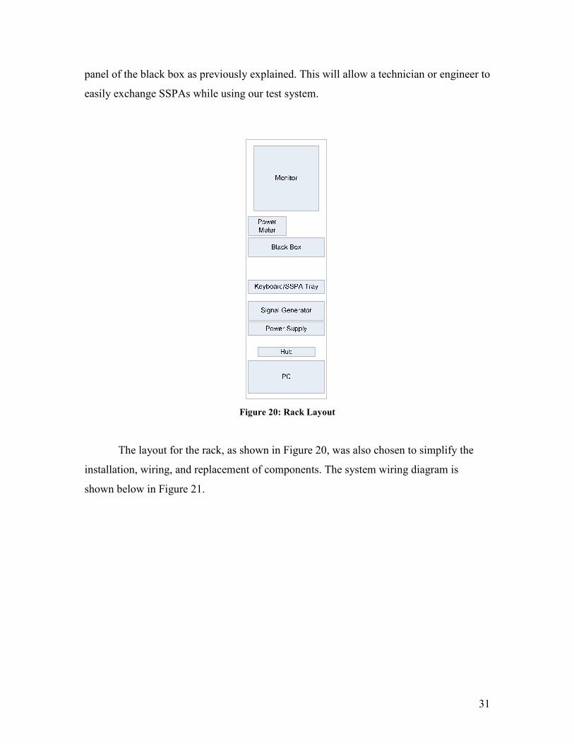
31
panel of the black box as previously explained. This will allow a technician or engineer to
easily exchange SSPAs while using our test system.
Figure 20: Rack Layout
The layout for the rack, as shown in Figure 20, was also chosen to simplify the
installation, wiring, and replacement of components. The system wiring diagram is
shown below in Figure 21.

32
Figure 21: System Wiring Diagram
6.2. Platform
Wikipedia has the following description in computing world for the word
Platform—“In computing, a platform describes some sort of framework, either in
hardware or software, which allows software to run. Typical platforms include a
computer's architecture, operating system, or programming languages and their runtime
libraries.”
6.2.1. Hardware Architecture
The Dell OptiPlex GX240 PC used for the ATS comprises Intel® 845 Chipset
with an Intel® Pentium® 4 2.0 GHz processor and L2 Cache of 512 KB. It belongs to the

33
80586 family of processors with the chipset bus speed of 400 MHz. The system memory
is limited to 512MB SDRAM with the system memory speed of 133 MHz. Since the
computer is an Intel® 80586 computer, with x86 (32-bit) bit architecture, it is able to
support both Windows and Linux as an operating system.
6.2.2. Operating System
The automated test suite is driven by a PC running Fedora Core 6 distribution of
Linux as an operating system. “Fedora Core is a free operating system that offers the best
combination of stable and cutting-edge software that exists in the free software world.”[5]
The Linux kernel version used in the system is 2.6.19-1.2895. The Fedora Project is Red
Hat sponsored open-source version of Red Hat Linux, which actually sets the benchmark
for Enterprise Linux. Linux operating systems supports multi-user logins as compared to
windows (except for Microsoft® Windows Servers) and hence multiple users can work
on the same system without having to depend on one another. Linux does not depend
upon RPC1 unlike Windows which uses RPC for almost every application. Linux has
been known to be more stable in comparison to Windows and the ever so important fact
of Linux being an open source and free by fat beats Windows by a wide margin.
As everything has advantages and disadvantages, there are some disadvantages in
using Linux as an operating system. Since Windows has more than 90% of the market, it
is very difficult to find support for Linux, especially for driver installations. As expected,
some problems were encountered during the driver installation of the GPIB interface card
and the NI-DAQ card. Both cards came in with drivers for Linux but not for Fedora Core.
The drivers provided by the National Instruments for both the GPIB and the DAQ cards
were supported only for Mandrake 10.1, Mandriva 2006, SUSE 10.0 / 10.1 and Red Hat
Enterprise WS 3/4 distributions of Linux.
It is possible to load the drivers for Red Hat Enterprise Distribution on Fedora
Core distribution because Fedora Core resembles Red Hat Enterprise distribution. There
were some modifications that were made to the install script because the Fedora
1 Remote Procedure Calls (calls made to other programs using APIs to do some other tasks)

34
distribution has some files located in different locations when compared to Red Hat. The
second step involved patching of the NI-KAL drivers. “NI-KAL is a low-layer driver that
is compiled when you install it on your machine. NI-KAL provides "glue" between your
Linux kernel and other National Instruments software. A version of NI-KAL is included
in every National Instruments Linux driver.” [6] Running the driver updates after the
patch resulted in successful installation of both the drivers and a fully operational system.
6.2.3. Programming Language
Out of the various different high level languages available in the commercial
market which include Java, C++, Microsoft Visual Studio .NET, Python, and Ruby,
Python was chosen for this project solely because the advantages of using Python
outweighed the drawbacks. After choosing Linux as the operating system, it was an easy
decision to use an open source programming language. Java is the first one that comes to
mind when someone talks about powerful open source programming languages, but
Python is not far behind either.
Python and Java are very distinct but equally prevailing. Python is essentially a
scripting language which can be extended as an object-oriented programming language
but the reasons taken into consideration are speed, ease of use, maintenance, and support.
Java being a compiler based programming language is faster because the processor only
has to load the pre-parsed byte code into the memory to execute the instructions. On the
other hand, Python, being an interpreted programming language, is easy to execute and
can be done on the fly after changes have been made to the source code; the programmer
need not go through the lengthy process of compiling the source code to the object code
and then linking the object code with the libraries using a linker. Another big advantage
of using Python is that it is dynamically typed (no variable declaration required) whereas
Java is statically typed (all variable names along with their types must be explicitly
declared). Python also allows the flexibility of assigning a variable with an object of a
different type even after it had been assigned to some other type whereas Java’s explicit
variable type declaration prohibits it from allowing such feature. The built-in arrays/lists,
hashes/dictionaries are significant advantages for Python over Java arrays and its library

35
based collections. Finally, the person who will be involved in maintenance and support of
the ATS is highly proficient in Python.
6.2.4. Database Management System (DBMS)
During the process of calibration and various tests performed on the SSPAs, the
ATS fetches sets of data for each of them. Storing that data becomes important for the
company to determine production yield, or if the designer wants to know the median for
various settings. Although saving data in a plain ASCII text file is convenient, it is not
convenient when there are thousands of records to handle. It is much easier to make use
of DBMS so that the data can be stored in organized manner and can be easily retrieved
in the format that the user wants by sunning simple SQL2 queries. There are many
database management software programs available in the market, e.g. Microsoft Access,
Oracle, Filemaker, Microsoft SQL Server, MySQL, and PostgreSQL.
PostgreSQL is a powerful, open source relational database system that can be
installed as a package during the installation of Fedora Core (project’s platform) or can
be separately installed. “It has more than 15 years of active development and a proven
architecture that has earned it a strong reputation for reliability, data integrity, and
correctness. It runs on all major operating systems, including Linux, UNIX (AIX, BSD,
HP-UX, SGI IRIX, Mac OS X, Solaris, Tru64), and Windows.” [7]
Similar to most of the commercial databases, it is fully ACID3 compliant,
supports foreign keys, table joins, views, triggers, functions, and stored procedures. It
also has native programming interfaces for C/C++, Java, .Net, Perl, Python, Ruby, Tcl,
ODBC, etc.
MySQL is a very popular open source database system in comparison to
PostgreSQL. MySQL, however, has many limitations while PostgreSQL provides those
2 Structured Query Language 3 Atomicity, Consistency, Isolation, and Durability (in terms of database management systems)

36
functionalities and flexibilities. Vita Voom Software talks about the advantages of
PostgreSQL over MySQL in their website4 which has been summarized below.
PostgreSQL is faster and more efficient than MySQL, supports unlimited row
sizes, unlimited database sizes, and tables up to 16TB. It also supports inheritance,
foreign keys, Unicode and is more resistant to crashes and power failures by using its
logging system. PostgreSQL supports functions (which can be used as stored procedures.
It supports outer joins and much more complex multi-joins than MySQL. It also supports
“limit” SQL keyword that can be used to limit the number of rows returned making
queries more responsive and resource economic. It supports subqueries, indexes on
functions and has more flexible BLOB field. Last but not the least, it is a RDBMS5 that
has grown alone, instead of MySQL which is a hack of several tools "glued" together
(MSQL, Berkeley DB).
To summarize our discussion over the choice of the database management system,
the key points that were taken into consideration for choosing PostgreSQL as the DBMS
for the project are listed below:
• Doesn't cost money even for commercial use. • Works at speed about the same as commercial databases. • Supports a broader subset of SQL than MySQL like sub-selects • Extremely responsive in high volume environments • Supports large tables that exceed Linux' file limit. • Fully Programmable. • Known to be legendarily reliable and stable
6.3. Software Architecture
Since the test station is automated, it has to be driven by software. Software is the
core of this project in terms of control and decision making. The ATS software is capable
of controlling all the ATS devices and can perform each and every task the device is
capable of programmatically. Software development includes program design, abstraction,
device interfacing, implementation and data storage.
4 http://www.vitavoom.com/postgresql.html 5 Relational Database Management System
37
6.3.1. Object Oriented Program Design
The purpose behind object oriented program design is simplification of complex
software design and goals. Object oriented design enables programmers to think at a very
high level about the available resources, their project goals, and how the goals can be
achieved with optimal use of their resources. Objects are essentially real world scenarios
or concepts tied together as collection of properties and attributes by object classes. The
real advantage of object oriented design is easy maintenance as each object is a stand-
alone entity and can be executed independent of others [1]. Another advantage of object
oriented programming is the ability to reuse object (or concepts) more than once in the
same sequence of instructions.
The SSPA Test Station appears straight forward, however, the logic that
automates the calibration and specification procedures are complex. Moreover, the
interfaces that communicate with the various drivers are even more intricate.
6.3.2. Device level Abstraction
All the devices that are used in the ATS are programmable. With object oriented
design concept, it was easy to segregate each individual device as individual object. The
specific properties and attributes of each device were constrained within its own object
class and these objects communicated with other object solely by message passing via
public methods of the object classes. Abstraction at the device level enabled us to take
baby steps one at a time and focus on one particular area at one particular instance.
6.3.3. Device Interfacing
Each device used in the ATS has its own device interfacing object class and hence
its own file. The protocol for the main program to communicate to the individual devices
was by creating object instances of individual devices and calling the public methods to
set or get values to and from the devices. Each device had different means of
communication with the PC and was implemented in a different way.

38
With today’s instruments getting more and more complex in terms of
development and capabilities, there needs to be a common standard means of
communication or interface language between computers and these programmable test
instruments. SCPI6 standard is one typical example of standards that companies are using
as interpreter between their hardware and software that controls them. “The SCPI
Standard is built on the foundation of IEEE-488.2, Standard Codes and Formats. It
requires conformance to IEEE-488.2, but is pure software standard.”[2] “IEEE-488.2
standard defines communication protocols that are necessary to effect application-
independent and device-dependent message exchanges, and further defines common
commands and characteristics useful in instrument system applications. It is intended to
apply to small-scale to medium-scale instrument systems comprised mainly of
measurement, stimulus, and interconnect devices outside the scope of the instrument
system environment.”[3]
SCPI command set comprises instructions that are simple and common “English-
like” syntax which are pure ASCII texts. With these new devices supporting SCPI, the
ease of use has definitely increased. The basic instruction set is common among almost
all the devices including the low level or register level programming instructions. Each
device can have additional high level instruction sets to accomplish some of the specific
tasks for which the device is designed.
GPIB Interface and Ethernet
The power meter connected to the PC via IEEE 488.2 GPIB interface while the
power supply and the signal generator were connected via Ethernet. Interfacing the power
supply and the signal generator with the PC was straight forward because of the Ethernet
connectivity. Using Berkley socket, simple TCP/IP connection was established with the
devices to send SCPI commands and receive readings and data as simple ASCII texts.
Controlling the GPIB interface card and establishing connection and communicating with
the instrument attached to this card required the knowledge of VISA7.
6 Standard Commands for Programmable Instrumentation 7 Virtual Instrument System Architecture

39
VISA was originally a specification developed by VXIplug&play Systems
Alliance as a step towards industry-wide software compatibility for multi-vendor VXI8
systems. However National Instruments defines VISA as “a standard for configuring,
programming, and troubleshooting instrumentation systems comprising GPIB, VXI, PXI,
Serial, Ethernet, and/or USB interfaces.”[4] National Instruments has also come up with
their own implementation of VISA I/O standard—NI-VISA. “NI-VISA includes software
libraries, interactive utilities such as NI Spy and the VISA Interactive Control, and
configuration programs through Measurement and Automation Explorer for all your
development needs.”[4]
VISA libraries are C/C++ library files and cannot be used in Python unless a
Python wrapper is built around the library. PyVisa package is one such wrapper built for
Python over C/C++ libraries that enables the programmer to control all kinds of
measurement equipment through various busses (GPIB, RS232, and USB) with Python
programs. PyVISA is tailored to work with arbitrary adapters from National Instruments,
Agilent, Tektronix, etc by making calls to the external library file bundled with the
hardware and the software of corresponding vendors. The use of PyVISA hides a lot of
low level programming required for device communication and enables the programmer
to think of what-to-do instead of how-to-do.
National Instrument’s Data Acquisition Card (DAQ)
The NI-DAQ 6220 card was used for all the functionalities that it was capable of
in addition to pure data acquisition and analog to digital conversion. The card is capable
of handling digital inputs and outputs along with generating timing pulse chains or
streams using its two counters. Both the counters were implemented to generate the TR
gating pulse and the RF gating pulse, with the RF gating pulse being 1µs inside the TR
gating pulse. Both pulse chains were of 20ms default period with the RF pulse operating
at 10% default duty cycle. The TTL outputs from the counters were used to drive the
pulse modulation switch for pulse modulation of the RF signal, the trigger for the power
meter as well as the trigger for data acquisition from the I/Q detector, which will be
8 VME eXtensions for Instrumentation
40
discussed later in this section. The digital inputs were used to read in the VSWR fault
status and the over temperature status lines from the SSPA. The SP6T9 load switch uses
TTL signals to switch between the 6 output ports. Five of the digital signals required to
switch between the five loads used in the ATS were also driven by the DAQ’s digital
outputs. The digital outputs were also used to drive the control circuitry of the SSPA.
Three digital lines were used to switch between different addresses during calibration,
one digital output to control the up/down line and one to control the increment line.
There were basically two ways of implementing the various DAQ functionalities
in Python; one was writing low level code for direct register level programming to
control the DAQ’s processor and the other was using C/C++ to code the functionalities
using the available library from National Instruments and writing a wrapper to export the
functions as shared libraries to Python. The latter option was more desirable as Python is
built on C construct and use of the library functions is more efficient and it also hides the
gory details involved in low level programming of embedded systems.
6.3.4. Class Modules
The software for the ATS was inherits object oriented design concepts and hence
the overall software is divided into modules, specifically known as class modules. The
modules are characterized as hardware controllers and process controllers. The hardware
controllers interface and control the programmable hardware, while the program flow
controllers organize the overall flow of the software. The hardware controllers are
discussed below. More information regarding the process controllers can be found in
Section 6.3.5
(a) Power Supply (PowerSupply.py)
The PowerSupply class module controls the Agilent power supply of the ATS via
the ethernet port. The module uses simple Berkley socket to establish connection and
SCPI commands to set voltage and current compliances and also to read the voltage and
9 Single-Pole-6-Throw

41
the current draw. The module is also capable of regulating the power on and off from the
power supply. The full implementation of the methods and their functionalities belonging
to this class can be found in Appendix D.
(b) Signal Generator (SignalGen.py)
The SignalGen class module manages the Agilent signal generator using the
ethernet port as well. The implementation of this module is similar to the PowerSupply
module and uses similar concepts. It also uses Berkley socket to establish connection and
SCPI commands to set RF power level, frequency compliance values. It is also capable of
switching on and off RF output from the device. The full implementation of the methods
and their functionalities belonging to this class can be found in Appendix D.
(c) Power Meter (PowerMeter.py)
The PowerMeter class module interfaces the Agilent power meter using the GPIB
card PyVisa python module. The module uses SCPI commands to read and write device
settings to and from the power meter. The power meter makes power measurements using
SCPI commands as well, but since the power meter is capable of making different types
of measurements related to power, specific settings need to be taken care of before
making measurements. The module, whenever initialized as an object by any other
process module, resets the power meter and sets it to our default settings.
The power meter settings handled by the PowerMeter class are listed below:
• Zero power-heads (both channels)
• Measurement type (peak power, average power)
• Measurement rate (single, double, fast)
• Trigger source (immediate, external)
• Trigger mode (continuous, single, free-run)
• Trigger delay (wait time after trigger before measurement)
• Wait for trigger (wait for external trigger before fetching data)
• Fetch trace data (digitized trace from each channel)
• Gain (correction factor)

42
The power meter has an advanced feature of getting the power level data trace. The
trace however can be fetched from the power meter only if the settings required to enable
this feature has been set in a specific order. The power meter has to be in single trigger
mode and the trace function has to be enabled. It should also be in wait for trigger mode
so that it starts getting the trace as soon as it encounters the external trigger. If these
settings are not set in this order, then the power meter throws Settings Conflict error.
This trace was used to perform two of the specification tests on an SSPA, namely
over-pulse test and droop test. The data fetched from the power meter was fed into
MATLAB to verify the results for these specification tests. The plot shown in Figure 22
was used to verify the output pulse limiting capability of the SSPA (within 2.5ms) for any
input pulse greater than the normal pulse width (2ms).
Figure 22. Plot of Output Power Trace (dBm) vs. Time (ms)
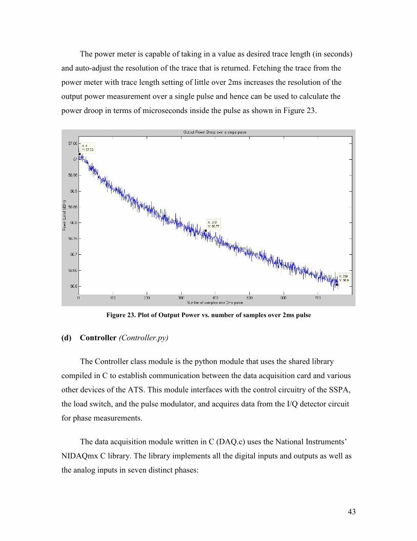
43
The power meter is capable of taking in a value as desired trace length (in seconds)
and auto-adjust the resolution of the trace that is returned. Fetching the trace from the
power meter with trace length setting of little over 2ms increases the resolution of the
output power measurement over a single pulse and hence can be used to calculate the
power droop in terms of microseconds inside the pulse as shown in Figure 23.
Figure 23. Plot of Output Power vs. number of samples over 2ms pulse
(d) Controller (Controller.py)
The Controller class module is the python module that uses the shared library
compiled in C to establish communication between the data acquisition card and various
other devices of the ATS. This module interfaces with the control circuitry of the SSPA,
the load switch, and the pulse modulator, and acquires data from the I/Q detector circuit
for phase measurements.
The data acquisition module written in C (DAQ.c) uses the National Instruments’
NIDAQmx C library. The library implements all the digital inputs and outputs as well as
the analog inputs in seven distinct phases:

44
• Create a task and channels and declare them as digital or analog
• Add created channels to the task
• Configure clock to be used for the task
• Define trigger source if needed
• Start the task
• Perform digital read, digital write or analog read
• Stop the task
The concept of tasks is verbose in the National Instruments’ library. Assigning
channels to a specific task makes it possible to reserve those particular channels and the
resources that have been assigned with the task when the task is started. Each task can be
run using different clock signals present internally in the DAQ. The base clock is a
20MHz oscillator and all other clocks are derivatives of this clock. Each task can also be
configured to await trigger signal, either analog or digital, on one of the Programmable
Function Interface (PFI) ports. The functions that fetch the data from the I/Q detector
(triggered by the RF pulse modulation signal) and the function that generate the RF pulse
modulation signal (triggered by the TR gating signal) use this feature. After setting the
configuration of the task it can be started and digital read/write or analog read can be
performed. Finally, it is very necessary to stop the task and release the handle of the
resources that were used, or else any subsequent calls would fail as it would not be able
to allocate the resource. Although the DAQ retains the output values on the digital output
ports, it has a limitation on the timers due to which it cannot retain the gating and the
pulse modulation signals. As an exceptional case, the 10% duty-cycle timing
functionality is implemented by defining task as static. The task is not stopped and
cleared at the end of the function, but at the beginning of the next function call. This way
the handle to the resource can be tracked as well as the timers are freely running.
The load switch, which is used to switch between five different loads during
different phases of calibration and production test, is controlled digitally using the digital
outputs from the data acquisition card. Five digital output lines go into the SSPA’s
control circuit to enable switch between different pots as well as to increase and decrease
the pot settings. Two digital lines are fed into the digital inputs of the DAQ to sense the
VSWR mismatch alarm and the over-temperature alarm given out by the SSPA.

45
The DAQ is configured to acquire data from the I/Q detector triggered by the RF
pulse modulations signal. The I/Q detector uses 1V as its reference voltage and outputs
differential voltages for both in-phase component and quadrature-phase componentsl
hence the outputs are at an offset of roughly ±1V. The data received from the I/Q detector
as read by the data-acquisition card has been presented as a plot below in Figure 24.
Figure 24. Plot of in-phase and quadrature-phase components of the phase of the RF output signal
As the outputs from the I/Q detector are at an offset, there was the need to acquire
data from the RF pulse modulation signal as well. This pulse modulation signal is used as
the reference for calculating the bias of individual signals as the pulse modulation signal
is just a TTL signal which has two states—low around 0V and high around 5V. The data
after filtering out the offset is represented in Figure 25.

46
Figure 25. Plot of in-phase, quadrature-phase, pulse modulation signal and phase in radians
(e) TempSensor (TempSensor.py)
The TempSensor class module rather than controlling the temperature sensor reads
the current temperature as outputted by the built in HTTP server within itself. The
temperature sensor is capable of reading 4 thermocouples at a time; for the ATS only one
is used. The module reads the data as html strings and parses the html string to read the
correct data. The temperatures are read in degree Fahrenheit.
6.3.5. Flow Control
The flow control or process control manages the entry point, exit point(s) and
sequential flow between processes. A software package typically has a single entry point
and effectively should have one exit point with proper implementation. The entry point
into the software execution is generally termed as the main routine. The main routine
controls the flow of the overall software and makes calls to other supporting procedures
by transferring control. While the subordinate procedure does some tasks, the main
control waits until it gets the control back. The idea of flow control for any software is
self explanatory if presented as a flow diagram or flow chart. The next five flow diagrams

47
represent the core of ATS’s software architecture—the first one is the main procedure
and the next four implement specific tasks that the ATS has been designed to handle.
Figure 26. Main Program Flow

48
Figure 27: Calibration Process Flow
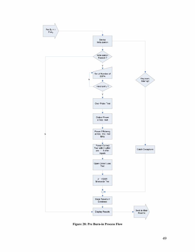
49
Figure 28: Pre Burn-in Process Flow
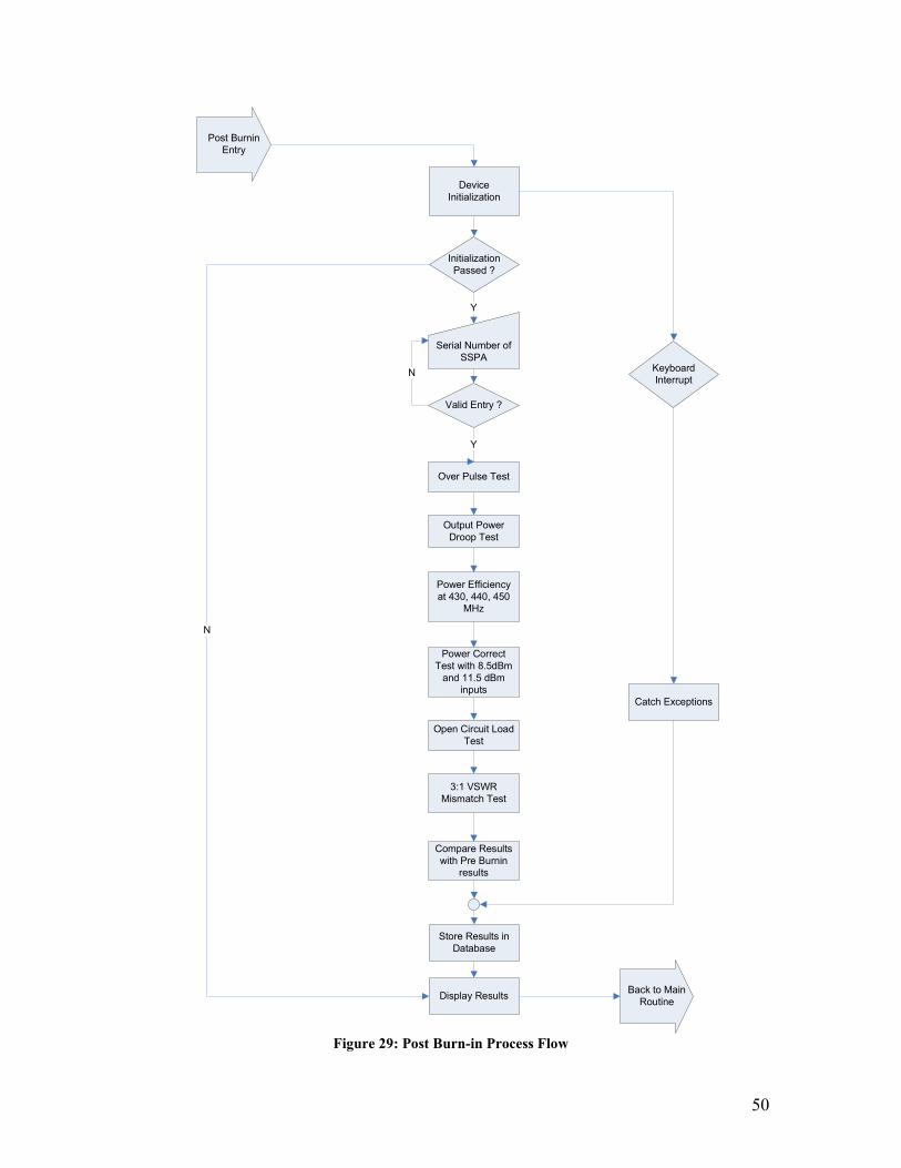
50
Post Burnin
Entry
Serial Number of
SSPA
N
Catch Exceptions
Keyboard
Interrupt
Over Pulse Test
Device
Initialization
Initialization
Passed ?
Y
N
Valid Entry ?
Y
Output Power
Droop Test
Power Efficiency
at 430, 440, 450
MHz
Open Circuit Load
Test
Power Correct
Test with 8.5dBm
and 11.5 dBm
inputs
3:1 VSWR
Mismatch Test
Display ResultsBack to Main
Routine
Store Results in
Database
Compare Results
with Pre Burnin
results
Figure 29: Post Burn-in Process Flow

51
Power Meter Offset
Calibration Entry
Catch Exceptions
Keyboard
Interrupt
Run Signal Generator at
10dBm
Device
Initialization
Initialization
Passed ?
Y
N
Signal Generator offset is
10 dBm - Ch. B reading
Set Signal Generator to
10 dBm with offset
Set Signal Generator to
17 dBm store Ch. B
reading
Ch. A offset is Ch. B
reading – Ch. A reading
Set Signal Generator to
17dBm
Display ResultsBack to Main
Routine
Ch. B Offset is Previous
Ch. B reading – current
Ch. B reading
N
User connects ‘Cable B’ to
‘Amp Input’
Did user make
connection?
Y
QUser connects ‘Cable B’ to
‘Channel B’ and ‘Amp Input’ to ‘Amp Output’
Did user make
connection?
Write offsets to offsets.ini
Figure 30: Power Meter Offset Calibration Flow

52
6.3.6. User Interface
The ATS software is accessible to the user via a terminal based user interface to
perform calibration and run various tests on an SSPA. The user interface provides the
user with options as main menu where the user just enters the number corresponding to
the process to be executed. A screen shot of the terminal based user interface is shown in
Figure 31.
Figure 31: Terminal based User Interface
The power supply, the signal generator and the power meter all had manual
controls on the instruments themselves, however, to carry out manual tests having control
over these three devices alone is not sufficient; having the control over the TR gating line,
RF gating line and to be able to manually switch between various loads is equally
important. The Graphical User Interface allows the user to control the gating lines and
load switch manually.

53
The GUI implemented using Python and Tkinter, which is a thin object-oriented
layer on top of Tcl/Tk. Tcl (Tool Command Language), is a powerful dynamic
programming language suitable for a very wide range of uses, including desktop
applications, networking, testing, etc. It is also an open source language that is cross
platform compatible. Tk, on the other hand, is a graphical user interface toolkit that is
used for developing desktop applications. Tk is the standard GUI for Tcl which can
produce rich, native applications that run unchanged across different platforms like
Windows, Mac OS X, Linux and many more.
Figure 32. Screenshot of the Manual Controls GUI
6.3.7. Exceptions and Error Handling
High-quality software ensures that the application does not crash due to the
actions of the user. It is also appropriate to display useful messages in case the software is
able to trap expected errors and exceptions. A program does not need to terminate in the
event of errors or exceptions; instead the system can revert back to its default conditions.
There are many places during the calibration and testing phases where exceptions can be
expected and therefore need to be handled. Typical examples include during initialization
of the devices. If the technician forgets to turn on the power supply or the ethernet
connection in the back of the signal generator is disconnected, the program should

54
provide warnings and possible solutions to fix the error and then be able to continue from
the same spot after the error has been fixed. In order to incorporate such expected cases, a
class that extended Python’s base Exception class was written implementing a set of
custom errors and exceptions. The list of expected and handled exceptions and errors
supported by the ATS are listed below.
device_error_PowerSupply : Cannot establish connection to the Power Supply
device_error_PowerMeter : Cannot establish connection to the Power Meter
device_error_DAQCard : Cannot establish connection to the DAQ
device_error_SignalGen : Cannot establish connection to the Signal Generator
device_error_SSPA_Power : Cannot establish connection to the SSPA
calib_initialCurrFailed : Initial current above 0.5A during Calibration
calib_gatePulseFailed : Current is above 0.5A with only gate pulse
calib_normalCurrFailed : Current is below 3A or above 5A
calib_driverCurrFailed : Current out of bounds while setting Driver Bias
calib_outputCurrFailed : Current out of bounds while setting Output Bias
calib_outputPowerFailed : Power out of bounds while setting Address 4
calib_phaseFailed : Phase out of bounds while setting Address 5
calib_vswrFailed : VSWR out of bounds while setting Address 6
calib_offsetCalibfailed : Power Meter Offset Calibration failed
offsets_ini_not_found : Offsets.init not found
process_abort_calib : Abort Calibration Process
process_abort_offsetcalib : Abort Offset Calibration Process
process_failed_offsetcalib : Offset Calibration
6.3.8. Database Programming and Data Storage
The project consists of five distinct test phases; hence the simplest database
schema would be to use a table for each type of test to be performed. This separates the
recorded measurements of one test from another, avoiding complications and the need to
write complex queries. Since the database consists of simple tables, independent of one
another, the concept of foreign key was never implemented because no complex relations
between tables exist. The database consists of eight separate tables that are unique to the
different tests conducted. These tables are listed below. Their respective table names are
shown in parenthesis and the data that is stored in each table is listed below each table
name.

55
• Calibration Data (calibration)
o Serial Number (sn)
o Date & Time (dt)
o Username (uname) o Initial Current (initcurrent)
o Current w/ TR only (trcurrent)
o Pot 1 Setting (pot1_set)
o Driver Bias Current (curr1)
o Pot 2 Setting (pot2_set)
o Output Bias Current (curr2)
o Current w/ TR & RF (trrfcurr)
o Initial Power (initpower)
o Pot 4 Setting (pot4_set)
o Final Power (power4)
o Output Current (curr4)
o Initial Phase (initphase)
o Pot 5 Setting (pot5_settings)
o Phase (phase)
o Phase Values (phase_values)
o Pot 6 Setting (pot6_set)
o Calibration Passed? (passed)
o Test Failure Code (test_fail_code)
• Pre Burn-in (preburnin)
o Serial Number (sn) o Date & Time (dt) o Username (uname) o Pulse Width (pulsewidth) o Overpulse Passed? (overpulse_passed) o Initial Droop Power (droop_initpower) o Final Droop Power (droop_finalpower) o Droop Passed? (droop_passed) o Current at 430MHz (current_430) o Current at 440MHz (current_440) o Current at 450MHz (current_450) o Voltage at 430MHz (voltage_430) o Voltage at 440MHz (voltage_440) o Voltage at 450MHz (voltage_450) o Power at 430MHz (power_430) o Power at 440MHz (power_440) o Power at 450MHz (power_450) o Power w/ 8.5dbm input (power_8_5) o Power w/ 11.5dbm input (power_11_5) o Input Variation Passed? (powercorrect_passed) o Open Load Passed? (open_passed)
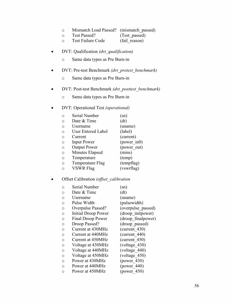
56
o Mismatch Load Passed? (mismatch_passed) o Test Passed? (Test_passed) o Test Failure Code (fail_reason)
• DVT: Qualification (dvt_qualification)
o Same data types as Pre Burn-in
• DVT: Pre-test Benchmark (dvt_pretest_benchmark)
o Same data types as Pre Burn-in
• DVT: Post-test Benchmark (dvt_posttest_benchmark)
o Same data types as Pre Burn-in
• DVT: Operational Test (operational)
o Serial Number (sn) o Date & Time (dt) o Username (uname) o User Entered Label (label) o Current (current) o Input Power (power_in0) o Output Power (power_out) o Minutes Elapsed (mins) o Temperature (temp) o Temperature Flag (tempflag) o VSWR Flag (vswrflag)
• Offset Calibration (offset_calibration
o Serial Number (sn) o Date & Time (dt) o Username (uname) o Pulse Width (pulsewidth) o Overpulse Passed? (overpulse_passed) o Initial Droop Power (droop_initpower) o Final Droop Power (droop_finalpower) o Droop Passed? (droop_passed) o Current at 430MHz (current_430) o Current at 440MHz (current_440) o Current at 450MHz (current_450) o Voltage at 430MHz (voltage_430) o Voltage at 440MHz (voltage_440) o Voltage at 450MHz (voltage_450) o Power at 430MHz (power_430) o Power at 440MHz (power_440) o Power at 450MHz (power_450)

57
o Power w/ 8.5dbm input (power_8_5) o Power w/ 11.5dbm input (power_11_5) o Input Variation Passed? (powercorrect_passed) o Open Load Passed? (open_passed) o Mismatch Load Passed? (mismatch_passed) o Test Passed? (Test_passed) o Test Failure Code (fail_reason)
Database Adapter and Data Access Layer
Psycopg2 is a PostgreSQL database adapter for the Python programming
language. It is the second version of the adapter which is a complete rewrite of the
original code to provide new style classes for connection and cursor objects and some
other additional features. Similar to the original psycopg, psycopg2 was written with the
aim of being small, fast, and stable.
Psycopg is different from other database adapters as it is designed for heavily
multi-threaded applications that create and destroy lots of cursors and make a
conspicuous number of concurrent INSERTs or UPDATEs. The sole reason behind using
psycopg over any other adapters like PygreSQL or PyPgSQL is because the adapter is
very intuitive and a lot of support is available online.
58
7. Twenty-Four Hour Burn-In System
Burn-in is meant to test a production unit’s capability to run under load for an
extended amount of time. The concept of burn-in is that you can reduce the probability of
a unit being defective in the field by running each production unit while monitoring for
malfunctions and errors. An additional benefit to burn-in testing is that it gives the
manufacturer more data that can used to judge the quality of production.
7.1. System Requirement
The SSPA’s burn-in system must be capable of running ninety-six amplifiers for
twenty-four consecutive hours. The amplifier must run at a frequency between 430MHz
and 450MHz at ten percent duty cycle. During the burn-in, the VSWR alarm and over-
temperature alarm status must be monitored. If an alarm trips during the burn-in test, then
the unit fails the burn-in test and the system should alert a technician.
7.2. System Design
The burn-in system needs to be able to run the amplifier under load and monitor
the alarm outputs. Each unit will have its own power supply and load because each
amplifier produces more than 500W of peak power and draws almost five amps of
current. It was decided that there would be one RF signal source and one transmit/receive
signal source for all ninety-six amplifiers. One pulse generator will be used and the
signals will be split to all amplifiers to minimize costs. The pulse generator must be
capable of producing a synchronized transmit/receive signal and RF modulation signal.
Because each of the amplifiers has two alarm signals that need to be monitored and the
transmit/receive signal needs to be split to each amplifier, it was decided that a
distribution circuit would be designed. The distribution circuit needs to latch to the alarm
signals from the SSPAs, alert the operator when a unit has been on for twenty-four hours,
and split the transmit/receive signal to all SSPAs. We chose to have only sixteen SSPAs
connect to each distribution circuit for simplicity.

59
7.3. Power Supplies
Each SSPA will have its own power supply. We will be using Mean Well 27V
power supplies. The SSPAs require 32V, so the power supplies will be adjusted up to that
voltage level.
7.4. Loads
Each SSPA will be producing five-hundred watts peak and needs to have that
energy dissipated in a matched load. We chose the MFJ model 264 and ran it at sixty
degrees Celsius for twelve hours to make sure that its load characteristics would not
change when used in a warm environment for long periods.
7.5. Signal Sources
The two signals that are required to operate an SSPA are the transmit/receive
signal and the RF signal. The RF signal is a pulse-modulated 10dBm continuous wave.
The pulses of RF must be within the pulses of the transmit/receive signal. This signal
enables the amplification stage and must be enabled during RF in order to properly
operate the SSPA. The RF signal is going to be generated using a phase-locked oscillator
(PLO) at 449 MHz. The PLO requires a 10MHz reference that can be provided by the
internal trigger of the Stanford Research Systems DG535 pulse generator chosen to create
the transmit/receive signal and the pulse modulation signal.
The DG535 is capable of creating the two pulses needed to properly time the
burn-in system. To operate an SSPA properly, the transmit/receive pulse must exceed the
RF input by at least one microsecond on both sides. The timing diagram can be found in
Appendix C.

60
7.6. Signal Distribution System
Having only one signal source for ninety-six amplifiers means that there needs to
be a distribution system that is capable of supplying the transmit/receive signal and
10dBm of RF to each amplifier. For simplicity, it was decided that the signal splitting
would be done in two stages.
The first stage of distribution amplifies the RF signal to compensate for power
losses due to splitting. This ensures that 10dBm will be present at the input of each SSPA
during the burn-in test. The splitter at this stage is an eight-way power splitter with ten
decibels of loss. Also in the first distribution stage is an eight-way buffer that is used to
split the transmit/receive signal eight ways.
The second stage of the distribution system splits each of the output signals from
stage one sixteen ways. The RF will be split using a two-way splitter going to two eight-
way splitters. We’re using two eight-way splitters instead of a sixteen-way splitter
because SRI already has six dual eight-way splitters that were designed and manufactured
for the AMISR panels available. Altogether, the loss due to stage two is fourteen decibels.
This stage of the distribution system is also to be used for providing information
to the technician running the burn-in tests. There are three indicators for each of the
sixteen amplifiers. One indicator shows the status of the VSWR alarm, one shows the
status of the over-temperature alarm, and the third shows whether the amplifier has been
running in the system for twenty-four hours.
The VSWR and over-temp indicators work identically. The alarm signal goes
through an inverter and clocks a flip-flop whose input is tied high. The outputs of the
flip-flop drive transistors that in turn drive the bi-color LEDs. The twenty-four hour
indicator uses the transmit/receive signal as a time-base to increment a counter. When the
counter reaches count 72,000, it clocks another flip-flop that is tied high. This flip-flop
controls the bi-color LED in the same manner as before, by driving transistors.

61
The alarm and time indicators need circuitry so that they can be reset when the
technician inserts a new SSPA to test. Instead of requiring the technician to press a reset
button for each amplifier he or she turns on, the reset circuitry will be activated by the
thirty-two volt supply voltage to the amplifier. The reset circuitry uses a comparator to
determine when the voltage supply exceeds twenty-eight volts. The comparator’s output
is connected to two flip-flops in series that are used with an AND gate to generate a pulse
on the rising edge of the comparator’s signal. The output of the AND gate is connected to
the reset inputs of all the indicators’ flip-flops. The benefit of the reset circuitry is to
avoid the possibility of the technician forgetting to reset the indicators when testing the
units.

62
8. Results
This section provides a sample of the data that the ATS will collect for each
amplifier. Table 9 is a sample of the calibration data that is collected for each SSPA that
is calibrated using the ATS. The actual database returns more data for each amplifier than
shown below. As shown below, in Tables 9 and 10, an engineer can easily analyze this
data and monitor manufacturing trends. The data shown below were collected by running
query on the custom views that were created within the database. The views enable the
user to view the data in a more readable and customized manner.
SN Driver
Bias Pot
Driver
Current
Output
Bias Pot
Output
Current
Output
Power Pot
Output
Power
Phase
Pot
Phase
(rads)
VSWR
Pot
Passed
5 74 0.303 77 0.505 69 57.216 75 1.670 24 YES
6 75 0.300 77 0.499 69 57.266 87 1.693 26 YES
7 73 0.295 68 0.501 54 57.209 57 1.745 64 YES
9 73 0.297 71 0.495 57 57.260 58 1.685 66 YES
10 35 0.297 45 0.496 100 56.964 NO Table 10: Sample Calibration Data
SN Init
Power
Final
Power
Droop
(%)
PWR
@ 430
Eff430
(%)
PWR @
440
Eff440
(%)
PWR @
450
Eff450
(%)
PWR
8.5dBm
5 57.135 56.61 11.39 57.72 39.32 57.18 39.32 57.35 39.32 57.13
6 57.294 56.794 10.87 57.90 40.4 57.38 40.4 57.67 40.4 57.27
7 57.29 56.777 11.15 57.51 41.89 57.27 41.89 57.30 41.89 57.26
9 57.269 56.703 12.23 57.38 37.62 57.28 37.62 57.57 37.62 57.25 Table 11: Sample Pre Burn-in Data
The unit that failed calibration during one of the runs (SN 10) as highlighted in
Table 9 above, failed due to the power output from the amplifier being less than 57.0dBm
after the pot was set to the maximum value of 100. Similarly, the unit that passed
calibration during one of the runs, but failed pre burn-in test (SN 9) is highlighted in red
in Table 10. The unit failed because the efficiency at all three measurement frequencies—
430MHz, 440MHz and 450MHz—was below 38%.

63
9. Conclusion
Our primary goal was to design a system to be used during production testing of
the Solid State Amplifiers (SSPA) used in the Advanced Modular Incoherent Scatter
radar (AMISR) being built by SRI International. The system needed to be capable of
calibrating each SSPA and conducting multiple tests including a twenty-four hour burn-in
test. To accomplish these tasks, we designed two independent systems.
The first system was the Automated Test Suite (ATS) and will be used to calibrate
the amplifiers as well as conduct a variety of specification tests. The system is fully
operational and is ready to begin testing amplifiers once production begins. The system
can also be easily modified to allow engineers to develop new tests in the future. We met
all of our goals for this system, including the capability of calibrating and conducting a
pre burn-in test in less than 5 minutes. The data collected during calibration and the other
test phases is collected and stored in a database that allows it to be easily exported to
excel. In the future SRI International will be able to design a custom interface that can be
used to monitor the testing of amplifiers from a remote location. There was also a limited
supply of amplifiers while we were designing the system. SRI International will need to
test more amplifiers to determine the standard for amplifiers being calibrated and tested
on the Automated Test Suite.
The second system in know as the Burn-in System. It will be used to conduct a
twenty-four hour operational test. The test consists of running ninety-six amplifiers at a
10% duty for a twenty-four hour period. This portion of our project consisted of design a
system that could use only one signal generator and a single source for the gate and RF
pulse signals to operate ninety-six amplifiers. The system was designed in two stages.
Currently the first stage has been completed and tested to verify it functions properly.
The second stage has not been finished; the second revision of the distribution board we
designed is currently being produced. Once the boards are returned and fully populated,
SRI International will need to construct and wire the rack system that will be used to test
ninety-six amplifiers.

64
References
1. Gnesi, Stefania. “Object Oriented Design.” Pisa, Italy: ISTI-CNR, 2000.
January 2007.
<http://fmt.isti.cnr.it/~gnesi/matdid/Object_oriented_dsfdesign.pdf>
2. IVI Foundation. “SCPI Consortium.” Niwot, CO. January 2007
<http://www.ivifoundation.org/Combined%20Organizations/SCPI.htm>
3. IEEE. “IEEE Std 488.2-1992 IEEE Standard Codes, Formats, Protocols, and
Common Commands for Use With IEEE Std 488.1-1987, IEEE Standard
Digital Interface for Programmable Instrumentation.” January 2007.
<http://standards.ieee.org/reading/ieee/std_public/description/im/488.2-
1992_desc.html>
4. National Instruments. “National Instruments VISA.” January 2007.
<http://www.ni.com/visa/>
5. Red Hat Inc. “Fedora™ Core 6.” January 2007. <http://fedora.redhat.com>
6. National Instruments. “National Instruments and Linux: Frequently Asked
Questions.” <http://www.ni.com/linux/support.htm#kal>
7. PostgreSQL. “About PostgreSQL.” January 2007.
<http://www.postgresql.org/about/>

1
Appendix A

1
Appendix B

1
Appendix C

1
Appendix D

1
Appendix E
Appendix A
Automated Test Suite User’s Guide
Authors:
Jeff Pelligrino John Scimone
Kaushal Shrestha
Date: February 26, 2007
A-1

Table of Contents 1. System Startup Instructions: .................................................................................. A-3 2. Using the ATS to test SSPA’s. .............................................................................. A-6 2.1. Production Test Package.................................................................................. A-7 2.2. Design Verification Test Package.................................................................... A-8 2.3. Manual Controls Package ................................................................................ A-9
A-2

1. System Startup Instructions:
Step 1: Plug grey ATS power cord into electrical outlet.
Step 2: Turn computer on.
Step 3: Turn computer monitor on.
A-3
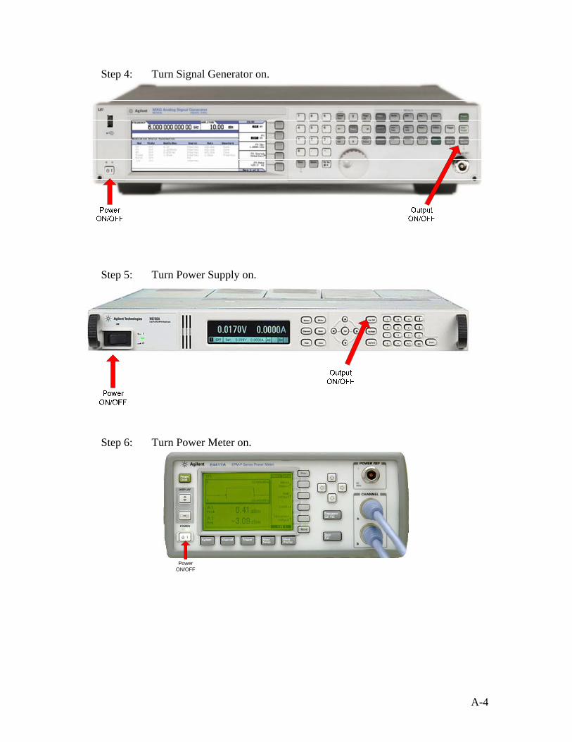
Step 4: Turn Signal Generator on.
Step 5: Turn Power Supply on.
Step 6: Turn Power Meter on.
PowerON/OFF
A-4

Step 7: Turn Control Box on. (Switch located on the rear of box)
Step 8: Verify Power Supply output is OFF. Step 9: Verify Signal Generator output is OFF. SYSTEM STARTUP COMPLETE.
A-5

2. Using the ATS to test SSPA’s.
There are 3 test packages available on the ATS.
• Production Test Package • Design Verification Test Package • Manual Controls Package
A-6

2.1. Production Test Package
Step 1: Select the desktop icon labeled “Production Test Package.” Step 2: Enter the username and press the <Enter> key.
Step 3: To select an option for the main menu, press the number on the keyboard corresponding to the option you want to select and press the <Enter> key.
A-7

2.2. Design Verification Test Package
Step 1: Select the desktop icon labeled “Design Verification Test Package.” Step 2: Enter the username and press the <Enter> key.
Step 3: To select an option for the main menu, press the number on the keyboard corresponding to the option you want to select and press the <Enter> key.
* If you select operational test, verify the SSPA is conducted and the environmental chamber is ready before starting the test
A-8

2.3. Manual Controls Package
Step 1: Select the desktop icon labeled “Manual Controls Package.” Step 2: Use load switch settings and timing card settings to conduct manual tests.
A-9

Appendix B
Control Box Technical Guide
SRI International
Automated Test Suite
Authors:
Jeff Pelligrino John Scimone
Kaushal Shrestha
Date: February 26, 2007
B-1
Table of Contents 1. Control Box Parts List ........................................................................................... B-3 1.1. I/Q Detector ..................................................................................................... B-4 2. Control Box Connections....................................................................................... B-7 2.1. Data Acquisition Card Connections................................................................. B-8 2.2. Load Switch Connections ................................................................................ B-9 2.3. Paragrine Switch Connections ....................................................................... B-10 2.4. Control I/O Connections ................................................................................ B-11 2.5. Amp DC Output Connections........................................................................ B-12 3. Control Box Wiring Diagram .............................................................................. B-13 4. Control Box Layout ............................................................................................. B-14 4.1. Internal Layout............................................................................................... B-15 4.2. Input Stage Couplers...................................................................................... B-16 4.3. Output Stage Coupler..................................................................................... B-16 4.4. Front Panel Layout......................................................................................... B-17 4.5. Back Panel Layout ......................................................................................... B-17
B-2

1. Control Box Parts List • Front Panel Connectors
o N-type to N-type Bulkhead Adaptor (Amp Output). o SMA to SMA Bulkhead Adaptor (Amp Input). o DB9 Panel Mount Receptacle (Control I/O). o 4-Pin Panel Mount Receptacle (Amp DC Output). o SMA to N-type Bulkhead Adaptor (Power Meter Ch. A). o SMA to N-type Bulkhead Adaptor (Power Meter Ch. B). o 120V AC Input with built-in switch and fuse.
• Back Panel Connectors
o 68-pin SCSI Panel Mount Receptacle (DAQ). o BNC to BNC Bulkhead Adaptor (Power Meter Ext. Trigger). o Agilent SP6T Load Switch. o SMA to N-type Bulkhead Adaptor (I/Q Detector Input). o N-type to N-type Bulkhead Adaptor (Load Switch Input). o N-type to SMA Bulkhead Adaptor (Signal Generator Input). o 2-pin Panel Mount Connector (Power Supply Input).
• Internal Components
o I/Q Detector* o Output Coupler: 30dBm o Input Coupler 1: 20dBm o Input Coupler 2: 20dBm o Attenuator: 30dBm o DAQ Breakout Box o Load Switch TTL Connector o Paragrine Switch o Power Supply: 5V o Power Supply: 24V
* See Section 1.1 of this document for detailed information regarding the I/Q Detector
B-3

1.1. I/Q Detector
The I/Q detector consists of the AD8347 Direct Conversion Quadrature Demodulator
chip implemented using its evaluation board. The functional block diagram for the
AD8347 is shown below, followed by the evaluation board schematic.
Functional Block Diagram
Evaluation Board Schematic
B-4

The evaluation board allows a user to implement filters to in-phase and
quadrature-phase signals. In this application low pass filters were implemented on the
evaluation board. These filters are shown below.
Figure 1: 7th order RF low pass filter
The evaluation board has pads that allow inductors and capacitors to be
implemented easily, however, pads are placed in a configuration suitable only for a pi-
network of inductors in series and capacitors in shunt. The filter was designed with the
cut-off frequency of 1 MHz with Bessel approach to get the maximally flat phase
response for the data acquisition card. The filter was designed on paper first and then the
performance of the filter was simulated using Agilent's Advanced Design System (ADS).
The values chosen for the inductors and the capacitors are standard values taken off Digi-
Key's catalog. The simulation results are show below.
B-5
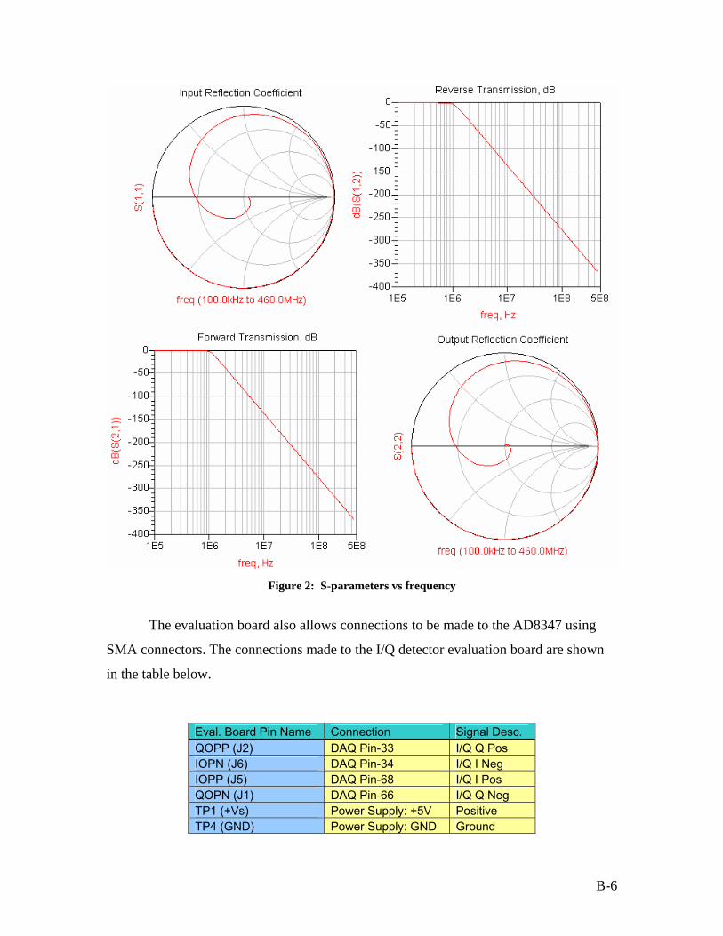
Figure 2: S-parameters vs frequency
The evaluation board also allows connections to be made to the AD8347 using
SMA connectors. The connections made to the I/Q detector evaluation board are shown
in the table below.
Eval. Board Pin Name Connection Signal Desc. QOPP (J2) DAQ Pin-33 I/Q Q Pos IOPN (J6) DAQ Pin-34 I/Q I Neg IOPP (J5) DAQ Pin-68 I/Q I Pos QOPN (J1) DAQ Pin-66 I/Q Q Neg TP1 (+Vs) Power Supply: +5V Positive TP4 (GND) Power Supply: GND Ground
B-6

2. Control Box Connections This section outlines connections made within the control box including:
• Data Acquisition Card Connections • Load Switch Connections • Paragrine Switch Connections • Amp DC Output Connections • Control I/O Connections
B-7

2.1. Data Acquisition Card Connections
Pin Pin Name Signal Name Connection Name Pin Pin Name Signal Name Connection Name 1 PFI 14/P2.6 68 AI 0 I/Q I Pos
Paragrine TTL Signal 67 AI GND 2 PFI 12/P2.4 RF Signal DAQ Pin-11 66 AI 9 I/Q Q Neg
Power Meter Ext. Trigger 65 AI 2 Thermo Cpl 2
3 PFI 9/P2.1 RF Trigger DAQ Pin 40 64 AI GND 4 D GND 63 AI 11 5 PFI 6/P1.6 Increment Amp DC Output (Grey) 62 AI SENSE 6 PFI 5/P1.5 61 AI 12 7 D GND 60 AI 5 8 +5 V (not 5V) 59 AI GND 9 D GND 58 AI 14
10 PFI 1/P1.1 VSWR Control I/O Pin-3 57 AI 7 11 PFI 0/P1.0 IQ Trigger 56 AI GND 12 D GND 55 NC 13 D GND 54 NC 14 +5 V Paragrine +5 53 D GND 15 D GND 52 P0.0 Address 0 Control I/O Pin-2 16 P0.6 Switch Path 4 Load Switch Logic Pin-9 51 P0.5 Switch Path 3 Load Switch Logic Pin-7 17 P0.1 Address 1 Control I/O Pin-4 50 D GND 18 D GND 49 P0.2 Address 2 Control I/O Pin-6 19 P0.4 Switch Path 2 Load Switch Logic Pin-5 48 P0.7 Switch Path 5 Load Switch Logic Pin-11 20 NC 47 P0.3 Switch Path 1 Load Switch Logic Pin-3 21 NC 46 PFI 11/P2.3 22 NC 45 PFI 10/P2.2 23 AI 15 44 D GND 24 AI GND 43 PFI 2/P1.2 Over Temp Control I/O Pin-1 25 AI 6 42 PFI 3/P1.3 26 AI 13 41 PFI 4/P1.4 27 AI GND 40 PFI 13/P2.5 TR Signal Control I/O Pin-9 28 AI 4 39 PFI 15/P2.7 29 AI GND 38 PFI 7/PP1.7 Up/Down Amp DC Output (Brown) 30 AI 3 Thermo Cpl 1 37 PFI 8/P2.0 31 AI 10 36 D GND 32 AI GND 35 D GND 33 AI 1 I/Q Q Pos 34 AI 8 I/Q I Neg.
B-8
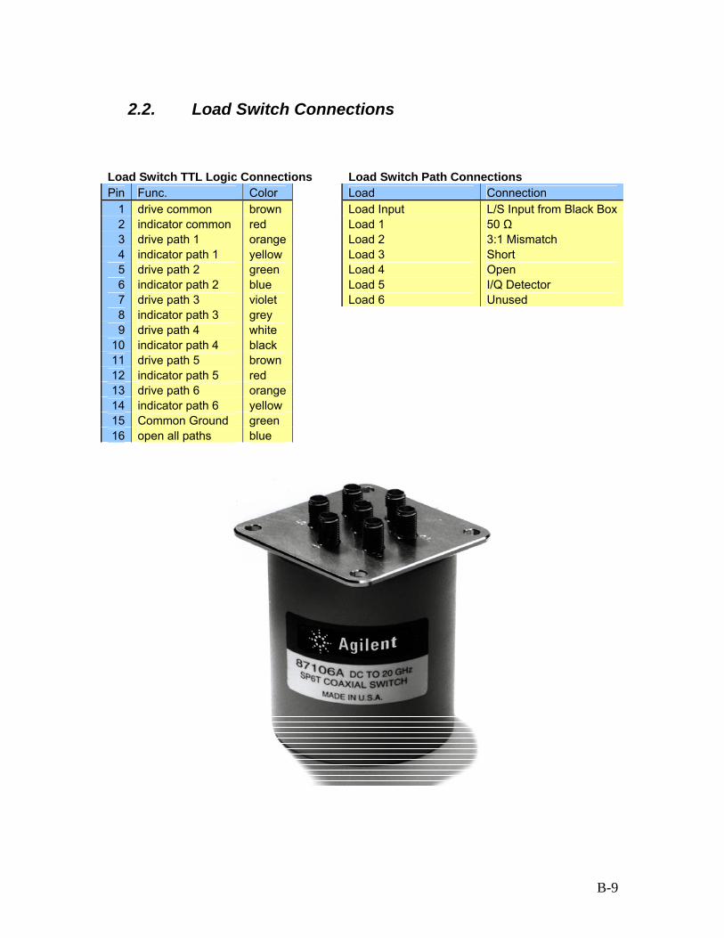
2.2. Load Switch Connections Load Switch TTL Logic Connections Load Switch Path Connections Pin Func. Color Load Connection
1 drive common brown Load Input L/S Input from Black Box2 indicator common red Load 1 50 Ω 3 drive path 1 orange Load 2 3:1 Mismatch 4 indicator path 1 yellow Load 3 Short 5 drive path 2 green Load 4 Open 6 indicator path 2 blue Load 5 I/Q Detector 7 drive path 3 violet Load 6 Unused 8 indicator path 3 grey 9 drive path 4 white
10 indicator path 4 black 11 drive path 5 brown 12 indicator path 5 red 13 drive path 6 orange 14 indicator path 6 yellow 15 Common Ground green 16 open all paths blue
B-9
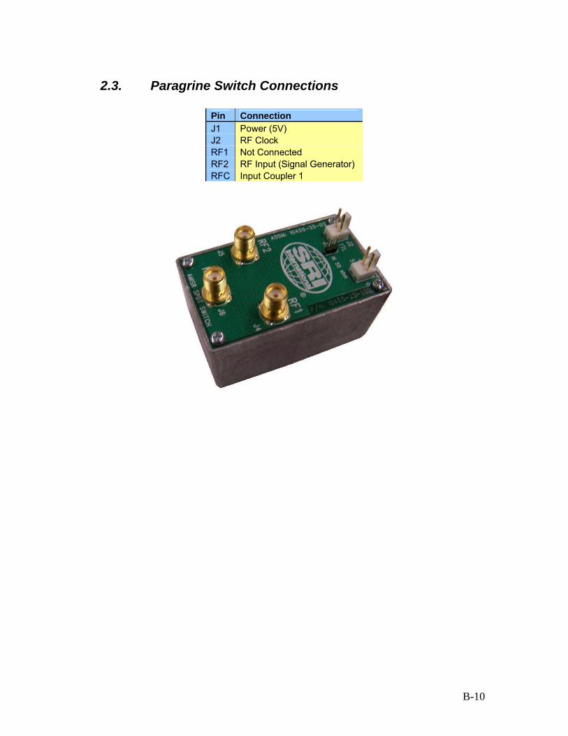
2.3. Paragrine Switch Connections
Pin Connection J1 Power (5V) J2 RF Clock RF1 Not Connected RF2 RF Input (Signal Generator) RFC Input Coupler 1
B-10
2.4. Control I/O Connections
Pin Color Connection 1 Black Temp. Status 2 Brown Address 0 3 Red VSWR Status 4 Orange Address 1 5 Yellow Gnd 6 Green Address 2 7 Blue Not Connected 8 Purple Gnd 9 Grey T/R
B-11

2.5. Amp DC Output Connections
Pin Color Connection 1 Red 32V 2 Gray Increment 3 Black Gnd 4 Brown Up/Down
B-12
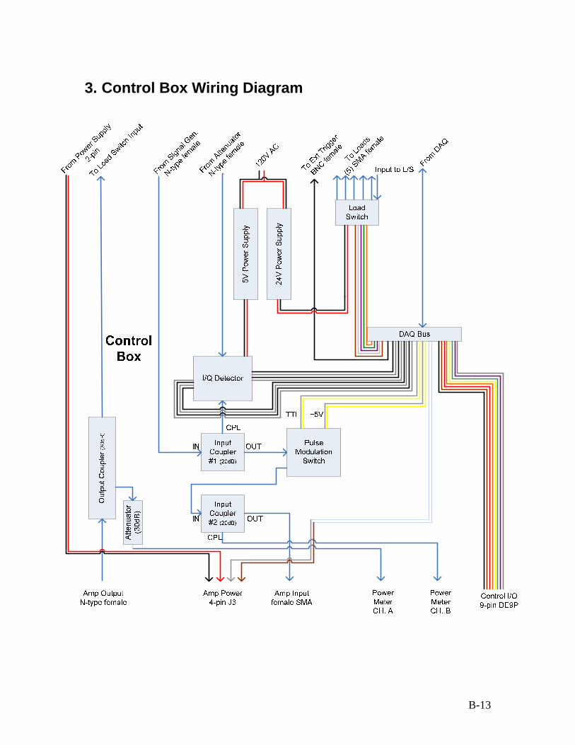
3. Control Box Wiring Diagram
B-13

4. Control Box Layout This section describes the layout of the control box including:
• Internal Layout • Input Stage Couplers • Output Stage Coupler • Front Panel • Back Panel
B-14

4.1. Internal Layout
InputCoupler#1 (20dB)
ParagrineSwitch
InputCoupler#2 (20dB)
I/Q Detector
DAQ BusControl
Box
Power Meter CH. A
Power Meter CH. B
120V
AC
From A
ttenu
ator
N-type
female
From Sign
al Gen
.
N-type
female To L
oads
(5) S
MA female
From P
ower
Supply
2-pin
To Ext
Trigge
r
BNC female
Amp Inputfemale SMA
Amp Power4-pin J3
Control I/O9-pin DE9P
Amp OutputN-type female
IN
CPL
OUT
IN OUT
CPL
TTL +5V
To Loa
d Switc
h Inp
ut
LoadSwitch
From D
AQ
B-15
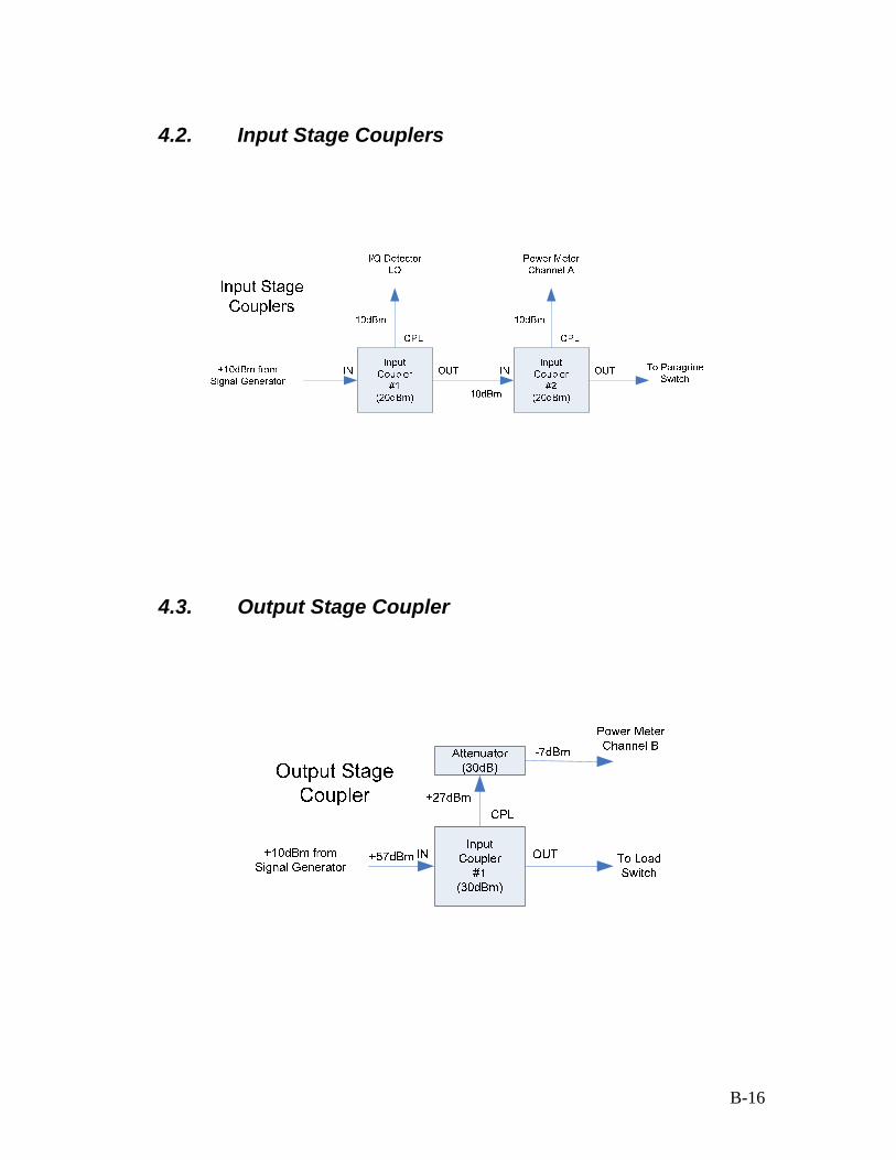
4.2. Input Stage Couplers
4.3. Output Stage Coupler
B-16
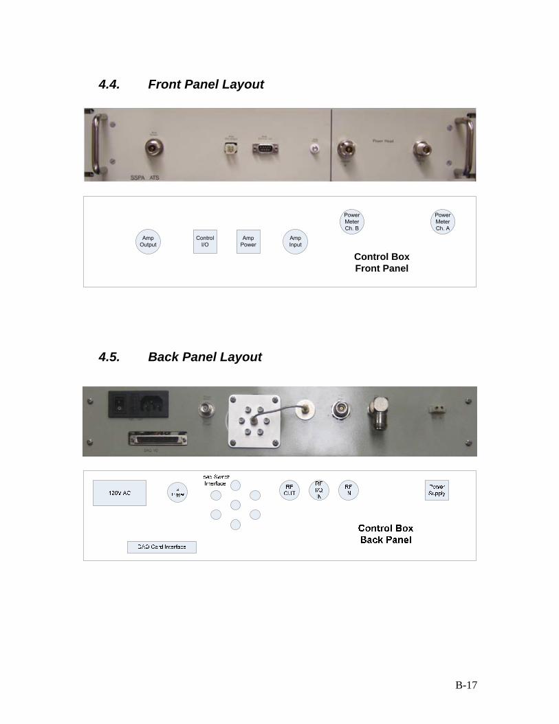
4.4. Front Panel Layout
Amp Input
Control Box Front Panel
Power Meter Ch. A
Power Meter Ch. B
Amp Output
AmpPower
ControlI/O
4.5. Back Panel Layout
B-17

Appendix C
Burn-in Technical Guide
Authors:
Jeff Pelligrino John Scimone
Kaushal Shrestha
Date: February 26, 2007
C-1

Table of Contents 1. Signal Distribution: Stage 1 Diagrams ................................................................... C-3 2. Signal Distribution: Stage 2 Diagrams ................................................................... C-4 3. Signal Distribution: Stage 2 Schematics................................................................. C-6
C-2
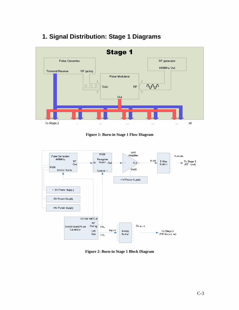
1. Signal Distribution: Stage 1 Diagrams
Figure 1: Burn-in Stage 1 Flow Diagram
Figure 2: Burn-in Stage 1 Block Diagram
C-3

2. Signal Distribution: Stage 2 Diagrams
Figure 3: Burn-in Stage 2 Flow Diagram
C-4
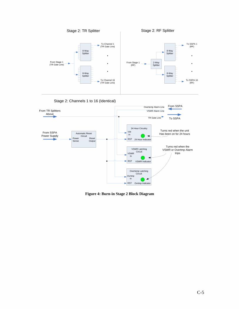
Automatic Reset Circuit
8-Way Splitter
From Stage 1(TR Gate Line)
Power Sense
ResetOutput
8-Way Splitter
To Channel 1(TR Gate Line)
To Channel 16(TR Gate Line)
.
.
.
Stage 2: Channels 1 to 16 (Identical)
24 Hour CircuitryT/RIn
RST
VSWR LatchingCircuit
VSWR In
RST
Overtemp LatchingCircuit
OvrtmpIn
RST
From SSPAPower Supply
From SSPA
VSWR Alarm Line
Overtemp Alarm Line
From TR SplittersAbove
To SSPATR Gate Line
24 Hour Indicator
VSWR Indicator
Ovrtmp Indicator
Stage 2: TR Splitter Stage 2: RF Splitter
8-Way Splitter
8-Way Splitter
2-WaySplitter
To SSPA 1(RF)
To SSPA 16(RF)
.
.
.From Stage 1
(RF)
Turns red when the unitHas been on for 24 hours
Turns red when the VSWR or Overtmp Alarm
trips
Figure 4: Burn-in Stage 2 Block Diagram
C-5

3. Signal Distribution: Stage 2 Schematics
Figure 5: TR Splitter and Power Connection Circuitry
C-6

Figure 6: Distribution Channel Circuitry
C-7

Appendix D
Programming Guide
SRI International Automated Test Suite
Authors:
Jeff Pelligrino John Scimone
Kaushal Shrestha
Date: February 26, 2007
D-1
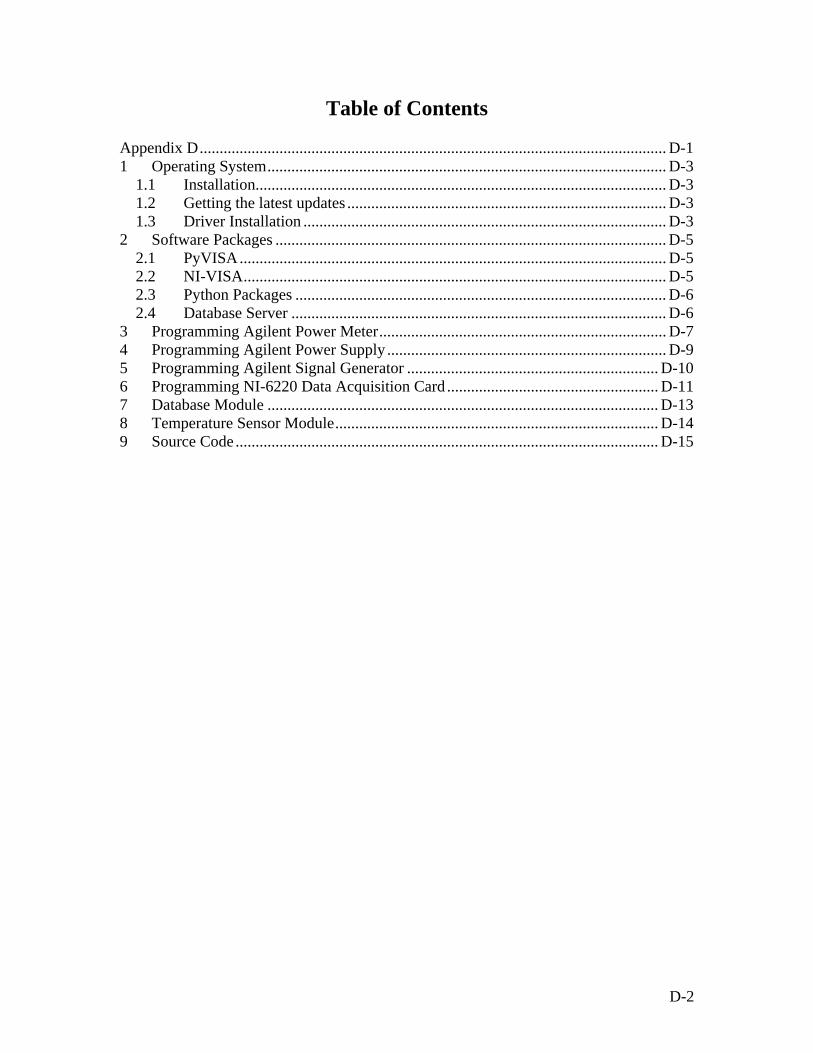
Table of Contents Appendix D..................................................................................................................... D-1 1 Operating System.................................................................................................... D-3
1.1 Installation....................................................................................................... D-3 1.2 Getting the latest updates ................................................................................ D-3 1.3 Driver Installation ........................................................................................... D-3
2 Software Packages .................................................................................................. D-5 2.1 PyVISA........................................................................................................... D-5 2.2 NI-VISA.......................................................................................................... D-5 2.3 Python Packages ............................................................................................. D-6 2.4 Database Server .............................................................................................. D-6
3 Programming Agilent Power Meter........................................................................ D-7 4 Programming Agilent Power Supply ...................................................................... D-9 5 Programming Agilent Signal Generator ............................................................... D-10 6 Programming NI-6220 Data Acquisition Card ..................................................... D-11 7 Database Module .................................................................................................. D-13 8 Temperature Sensor Module................................................................................. D-14 9 Source Code .......................................................................................................... D-15
D-2

1 Operating System Fedora Core 6 is readily available online because it is an open source operating
system. The ISO image file of the installation DVD can be downloaded from
1. Fedora’s download site (http://fedora.redhat.com/Download/), or
2. Mirror sites (http://fedora.redhat.com/Download/mirrors.html), or
3. BitTorrent (http://fedoraproject.org/wiki/Distribution/Download/BitTorrent).
The complete release notes and the installation guide can be found under Fedora’s
documentation section at http://fedora.redhat.com/docs/ .
1.1 Installation The installation process is very easy and intuitive. It is as simple as booting from the
DVD and proceeding through the installation with default settings. Do a clean install on
the hard drive by selecting to format the partition that you want to install Fedora Core 6
with minimal options.
1.2 Getting the latest updates Getting the latest update for the working kernel is important along with other updates.
Fedora Core has a built in program that searches all the repositories for all available
updates that are possible for the current system and configuration. Open up the terminal
and as root type the following command to get the updates.
# yum update
1.3 Driver Installation All the hardware present in the Automated Test Suite (ATS) PC is detected by
Fedora’s installer, except for the National Instruments’ GPIB card and the DAQ card.
1. Installing NIDAQ card Step 1: Insert the CD that came with the ATS
Step 2: Create a symbolic link to asm-offsets.h by typing the following in the
terminal window:
D-3

# ln -s /lib/modules/$(uname -r)/ source/include/asm/asm-offsets.h
/lib/modules/$(uname -r)/source/include/asm/asm_offsets.h
Step 3: Open /lib/modules/$(uname -r)/source/include/linux/utsrelease.h and
copy the line #define UTS_RELEASE "2.6.xx-1.xxxx.fc6", into
/lib/modules/$(uname -r)/source/include/linux/version.h, and save it.
Step 4: As root run the install script from the CD and use the default installation
paths for everything.
# <CD-Mount Directory>/NI-DAQ/INSTALL
Step 5: When INSTALL finishes, do not reboot.
Instead patch the nikal using the file found in the Patch directory of the
CD using the following command.
# patch -p0 < nikal.patch
Step 6: Copy the modprobe file ‘modpost’ from the Patch directory of the CD to
/lib/modules/$(uname -r)/source/scripts/mod/
Step 7: Run updateNIDrivers and reboot.
2. Installing GPIB card Step 1: Insert the CD that came with the ATS
Step 2: Create a symbolic link to asm-offsets.h:
# ln -s /lib/modules/$(uname -r)/ source/include/asm/asm-offsets.h
/lib/modules/$(uname -r)/source/include/asm/asm_offsets.h
Step 3: Open /lib/modules/$(uname -r)/source/include/linux/utsrelease.h and
copy the line #define UTS_RELEASE "2.6.xx-1.xxxx.fc6", into
/lib/modules/$(uname -r)/source/include/linux/version.h, and save it.
Step 4: As root run the install script from the CD and use the default installation
paths for everything.
# <CD-Mount Directory>/NI-488225L/INSTALL
Step 5: When INSTALL finishes, do not reboot.
Instead patch the nikal using the file found in the Patch directory of the
CD using the following command.
# patch -p0 < nikal.patch
D-4

Step 6: Copy the modprobe file ‘modpost’ from the Patch directory of the CD to
/lib/modules/$(uname -r)/source/scripts/mod/
Step 7: Run updateNIDrivers and reboot.
2 Software Packages Before proceeding with installing software packages that are required to successfully
run the ATS software, make sure that Python programming environment was installed
during the native installation of Fedora Core 6. In case you forgot to install Python,
running yum as root from the shell will install it.
# yum install python
2.1 PyVISA PyVISA is needed by the ATS software to communicate with the Agilent power
meter via the National Instrument GPIB interface using Python. PyVISA can be
downloaded from the internet (http://pyvisa.sourceforge.net/). Alternatively, it can be
installed by installing the RPM file from PyVISA directory of the Installation CD. The
RPM can be installed by browsing the directory using the GUI and double-clicking the
PyVISA-1.1-1.noarch.rpm RPM file, or by typing the following command as root.
# rpm -install PyVISA-1.1-1.noarch.rpm
2.2 NI-VISA PyVISA is a Python wrapper for National Instruments’ VISA Library. The NI-VISA
Library must be installed before PyVISA can be functional from within Python. To install
NI-VISA library run the install script as root.
# <CD-Mount Directory>/NI-VISA/INSTALL
D-5

2.3 Python Packages There are some additional Python packages that need to be installed to get the ATS
fully operational. The packages namely are python-ctypes, pytz, and python-psyzopg2
which do not come with the native install of Fedora Core 6. They can be installed by
running the yum command as root.
# yum install python-ctypes pytz python-psyzopg2
2.4 Database Server The ATS uses PostgreSQL as the database server. If the PostgreSQL server was not
installed during the installation of Fedora Core, it is readily available via yum. Install the
database server using ‘yum’ as root.
# yum install postgresql-server
By default, the Postgres databases can only be accessed by root or postgres users.
The user should login as root or the postgres and create a database (preferably ‘SSPA’)
using the command createdb.
# su – postgres
$ createdb sspa
The database can be deleted by using the dropdb command.
$ dropdb sspa
The default database schema for the ATS is provided in the Installation CD and can
be imported into the database created by using psql (client for PostgreSQL).
$ psql sspa < <CD-Mount Directory>/Database/SSPA-schema.sql
D-6

3 Programming Agilent Power Meter The Agilent Power Meter is controlled specifically by the PowerMeter class in
PowerMeter.py and the methods within the class. The functions available within the
power meter class are listed below with their functionalities.
Public Functions:
a. getMeasInput() • Gets a peak power measurement from power head channel A.
b. getMeasOutput()
• Gets a peak power measurement from power head channel B.
c. getTraceData() • Gets the trace data from Power Head Channel B. • Accepts length of trace (ms).
o By default, tracelength = 0.02. • Accepts length of trigger delay (ms).
o By default, triggerdelay = 0.
d. zeroPowerHeads() • Zeros power meter channel A and power meter channel B.
e. setFreq()
• Sets the frequency of power meter channel A and B. • Accepts a frequency (MHz).
o By default, freq = 440. Private Functions:
a. __setCaptureRate() • Sets the measurement speed on power meter channel A and B • Accepts the measurement speed mode: “NORMAL”, “DOUBLE”, or
“FAST”. o By default, mode = “DOUBLE”
b. __setMeasurementSettings()
• Sets power measurement mode, trigger mode, and trigger source • Accepts measurement mode: “PEAK”, or “AVER”
o By default, pow = “peak” • Accepts trigger mode: “CONT”, or “IMM”
o By default, mode = “CONT” • Accepts trigger source: “BUS”, “EXT”, “HOLD”, “IMM”, or “INT”
o By default, trigger = “EXT”
D-7

c. __setTriggerDelay()
• Sets the trigger delay for power meter channel A and B. • Accepts a length of time (s).
o By default, delay = 100e-6. o
d. __setTraceUnits() • Sets the trace function units on power meter channel A and B.
e. __enableTrace()
• Enables the trace capture for power meter channel B.
f. __setPowMeasurement() • Set the power measurement type for power meter channel A and B. • Accepts a measurement mode: “PEAK” or “AVER” • By default, type = “PEAK”.
g. __setTrigger()
• Sets the trigger mode for power meter channel A and B. • Accepts a trigger mode: “EXT” or “IMM” • By default, trigger = “EXT”.
h. __waitTrigger()
• Sets power meter channel A and B in wait for trigger state.
i. __getOffsetInput() • Gets dB loss offset or input stage.
j. __getOffsetOutput()
• Gets dB loss offset for output stage.
D-8

4 Programming Agilent Power Supply The Agilent Power Supply functions are available in the PowerSupply class in the
PowerMeter.py file and the methods within the class control the functionalities provided
by the power supply. The functions available within the class are listed below with their
functionalities.
Public Functions:
a. setCurr() • Sets the current limit. • Accepts a current value (A).
b. getVoltageSetpoint()
• Returns the power supply voltage level setting.
c. setVolt() • Sets the voltage limit. • Accepts a voltage value (V).
d. getCurr()
• Returns the power supply current level setting.
e. getVoltageReading() • Measures the output voltage. • Returns the measured value.
f. setPowerOn()
• Enables the power supply output and allows the capacitors to charge.
g. setPowerOff() • Disables the power supply output.
h. getPowerStatus()
• Returns the power supply output status (on/off).
D-9

5 Programming Agilent Signal Generator The Agilent Signal Generator functions are available in the SignalGen class in the
SignalGen.py file. These functions / methods within the class control various
functionalities of the signal generator. The functions available within the class are listed
below with their functionalities.
Public Functions:
a. setRFOff() • Disables the RF output of the signal generator.
b. setRFOn()
• Enables the RF output of the signal generator.
c. setAmplitude() • Sets the RF output amplitude of the signal generator. • Accepts an amplitude (dBm) between -110dBm and 17dBm.
d. setFreq()
• Sets the RF output frequency of the signal generator. • Accepts a frequency (Hz) between 250kHz and 1GHz.
Private Functions:
a. __getOffsetOutput() • Gets dB loss offset for the output stage.
D-10

6 Programming NI-6220 Data Acquisition Card The controller class is used to control the data acquisition card. The functions
available within the controller class are shown below. The functions available in the
Controller.py file make calls to the shared object file compiled using GNU C and
nidaqmx library provided by National Instruments.
Public Functions:
a. getPhase() • Gets the phase of an amplifier in radians.
b. getPhaseD()
• Gets the phase of an amplifier in degrees.
c. getPhaseValues() • Gets the in-phase and quadrature phase values in radians.
d. getPhaseValuesD()
• Gets the in-phase and quadrature phase values in degrees.
e. getVSWR_Flag() • Returns the status of the VSWR flag.
f. getTemp_Flag()
• Returns the status of the temperature flag.
g. setAddr() • Sets the address. • Accepts a number between 0 and 7 inclusive.
h. setLoad()
• Sets the load switch path. • Accepts a number between 1 and 5 inclusive.
i. setIncr()
• Sets increment. • Accepts either 1 or 0.
j. setUpDown()
• Sets UpDown. • Accepts either 1 or 0.
D-11

k. Increment() • Toggles setIncr() a specified amount while UpDown is high. • Accepts the number of times setIncr() will be toggled.
o By default, number_of_pulses = 1.
l. Decrement() • Toggles setIncr() a specified amount while UpDown is low. • Accepts the number of times setIncr() will be toggled.
o By default, number_of_pulses = 1.
m. setTR() • Sets the TR gate line pulse. • Accepts a value for on/off: 0 or 1. • Accepts the period of the pulse (s).
o By default, period = 20e-3*. • Accepts the pulse width (s).
o By default, pw = 2e-3*.
*Since the RF pulse needs to be within the TR pulse, the python wrapper for the DAQ will increase the period and pulse width of the TR gate line by 2µs. This will envelope the RF gate line within the TR gate line when they use their default pulse widths and periods.
n. setRF()
• Sets the RF gate line pulse. • Accepts a value for on/off: 0 or 1. • Accepts the period of the pulse (s).
o By default, period = 20e-3. • Accepts the pulse width (s).
o By default, pw = 2e-3.
o. setRFHigh() • Sets the RF gate line high.
p. setRFLow()
• Sets the RF gate line low.
D-12
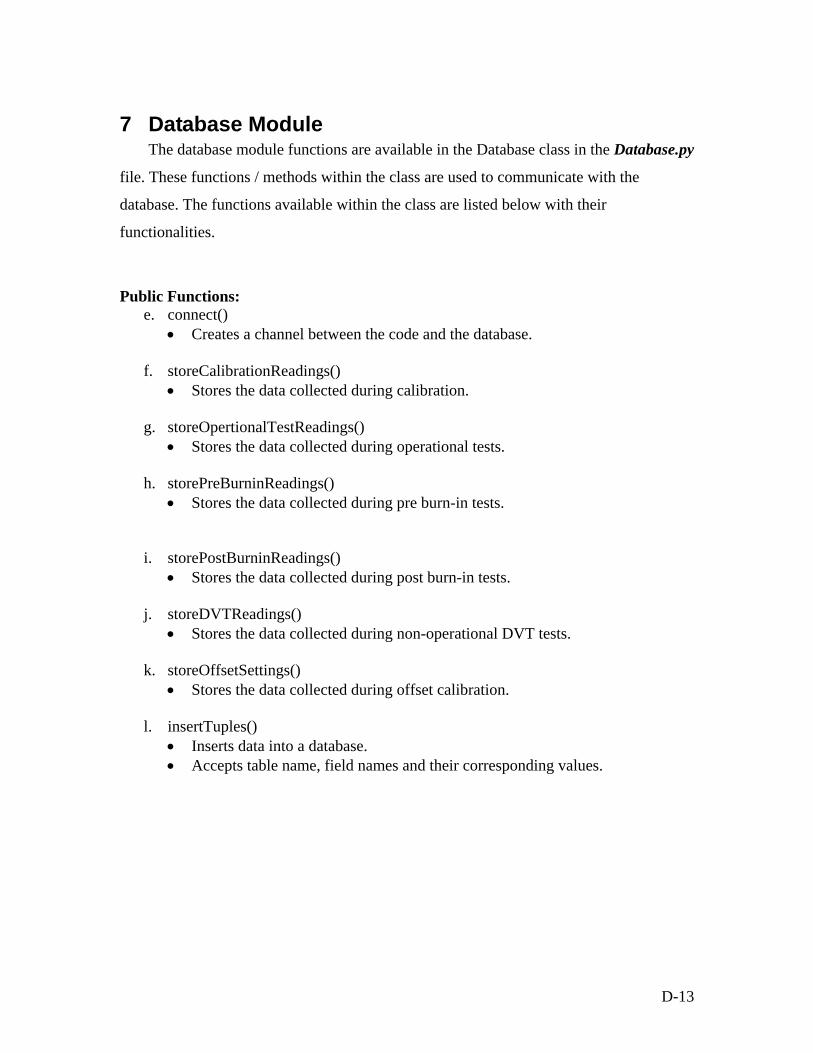
7 Database Module The database module functions are available in the Database class in the Database.py
file. These functions / methods within the class are used to communicate with the
database. The functions available within the class are listed below with their
functionalities.
Public Functions:
e. connect() • Creates a channel between the code and the database.
f. storeCalibrationReadings()
• Stores the data collected during calibration.
g. storeOpertionalTestReadings() • Stores the data collected during operational tests.
h. storePreBurninReadings()
• Stores the data collected during pre burn-in tests.
i. storePostBurninReadings() • Stores the data collected during post burn-in tests.
j. storeDVTReadings()
• Stores the data collected during non-operational DVT tests.
k. storeOffsetSettings() • Stores the data collected during offset calibration.
l. insertTuples()
• Inserts data into a database. • Accepts table name, field names and their corresponding values.
D-13

8 Temperature Sensor Module The Temperature Sensor functions are available in the TempSensor class in the
TempSensor.py file. These functions / methods within the class are used to receive data
from the SensaTronics temperature sensor. The functions available within the class are
listed below with their functionalities.
Public Functions: a. getTemperature()
• .Calls a private function to get the temperature data. Private Functions:
a. __getSensaTronicTemp(sensor) • Gets temperature reading from the designated sensor.
D-14

9 Source Code
SRI International Automated Test Suite
D-15

#!/usr/bin/env python
import Controllerimport PowerMeterimport PowerSupplyimport SignalGen
import Database
import timeimport stringimport sysimport math
from TestException import *from Utilities import *
warmup_period = 3 # Scalibration_freq = 444e6 # Hzinitcurrent_max = 0.6 # Anormcurrent_max = 5 # Anormcurrent_min = 2 # A
class Calibration: def __init__(self, uName): self.powersupply = PowerSupply.PowerSupply() self.siggen = SignalGen.SignalGen() self.powermeter = PowerMeter.PowerMeter() self.controller = Controller.Controller() self.user = uName self.siggen.setFreq( calibration_freq ) #Calibration at this freq self.powermeter.setFreq( calibration_freq )
def destructor(self): # Issues with using the default __del__() try:
del self.controller del self.siggen del self.powersupply except Exception, ex: raise
# ******************************************************************** # # Start of "Public Functions" Block # # ******************************************************************** def runCalibration (self, serialno = ""): values = " sn" : " ", " uname" : " ", " initcurrent" : " ", " trcurr" : " ", " pot1_set" : " ", " curr1" : " ", " pot2_set" : " ", " curr2" : " ", " trrfcurr" : " ", " pot4_set" : " ", " initpower" : " ", " power4" : " ", " curr4" : " ", " pot5_set" : " ", " phase" : " ", " pot6_set" : " ", " initphase" : " ", " phase_values" : " " # Values dictionary
while serialno ≡ "":
Feb 28, 07 8:10 Page 1/10Calibration.py print "" sn = raw_input(" Please enter the Serial Number of the SSPA :") serialno = str(sn).strip().replace(" "," _") values[’ sn’] = " ’%s’" % serialno values[’ uname’] = " ’%s’" % self.user # ========================================== # First Stage of Calibration # Startup # ========================================== sys.stdout.write ( " \nStarting Calibration Process ...\n" )
self.siggen.setRFOff() #From signal generator
self.controller.setLoad(self.controller.load_50_ohms) self.powersupply.setPowerOff() self.powersupply.setVolt(32) self.powersupply.setCurr(1)
print " Turning on Power Supply for initial current measurement"
self.powersupply.setPowerOn() current = self.powersupply.getCurr() sys.stdout.write( " Initial current draw of %.0f mA...\t" % \ (current*1000)) sys.stdout.flush() values[’ initcurrent’] = (" %s" % current)
if ( current > initcurrent_max ): self.__saveCalibrationResults( \ values, 0, TestException.calib_initialCurrFailed) setStyle(’ bold’, ’ red’) sys.stdout.write ( " [ FAILED ]\n" ) setStyle(’ default’) raise TestException(TestException.calib_initialCurrFailed) elif (current < 0): setStyle(’ bold’, ’ red’) sys.stdout.write ( " [ FAILED ]\n" ) setStyle(’ default’) self.__saveCalibrationResults( \ values, 0, TestException.device_error_SSPA_Power) raise TestException(TestException.device_error_SSPA_Power) else: setStyle(’ bold’, ’ green’) sys.stdout.write ( " [ OK ]\n" ) setStyle(’ default’) # End of First Stage # ==========================================
# ========================================== # Second Stage of Calibration # Initialize Digital Potentiometers # ========================================== print " Initializing digital potentiometers..." countAddr1 = 0 countAddr2 = 0 countAddr4 = 50 countAddr5 = 50 countAddr6 = 50 # −−−−−−−−−−−−−−−−−−−−−−−−−−−−−−−−−−−−−−−−−− # Set Addr 1 (Driver Stage −− Bias) # −−−−−−−−−−−−−−−−−−−−−−−−−−−−−−−−−−−−−−−−−− print " Resetting pot 1−−driver bias−−to %s" % countAddr1 self.controller.setAddr(1) self.controller.setTR(0)
Feb 28, 07 8:10 Page 2/10Calibration.py
Printed by Kaushal Shrestha
Wednesday February 28, 2007 1/36Calibration.py

self.controller.Decrement(100)
# −−−−−−−−−−−−−−−−−−−−−−−−−−−−−−−−−−−−−−−−−− # Set Addr 2 (Output Stage −− Bias) # −−−−−−−−−−−−−−−−−−−−−−−−−−−−−−−−−−−−−−−−−− print " Resetting pot 2−−output bias−−to %s" % countAddr2 self.controller.setAddr(2) self.controller.setTR(0) self.controller.Decrement(100)
# −−−−−−−−−−−−−−−−−−−−−−−−−−−−−−−−−−−−−−−−−− # Set Addr 4 (Power Level) # −−−−−−−−−−−−−−−−−−−−−−−−−−−−−−−−−−−−−−−−−− print " Resetting pot 4−−power level−−to %s" % countAddr4 self.controller.setAddr(4) self.controller.setTR(0) self.controller.Decrement(100) self.controller.Increment(countAddr4) # Set the pot to the middle
# −−−−−−−−−−−−−−−−−−−−−−−−−−−−−−−−−−−−−−−−−− # Set Addr 5 (Phase) # −−−−−−−−−−−−−−−−−−−−−−−−−−−−−−−−−−−−−−−−−− print " Resetting pot 5−−phase−−to %s" % countAddr5 self.controller.setAddr(5) self.controller.setTR(0) self.controller.Decrement(100) self.controller.Increment(countAddr5)
# −−−−−−−−−−−−−−−−−−−−−−−−−−−−−−−−−−−−−−−−−− # Set Addr 6 (VSWR) # −−−−−−−−−−−−−−−−−−−−−−−−−−−−−−−−−−−−−−−−−− print " Resetting pot 6−−vswr alarm−−to %s" % countAddr6 self.controller.setAddr(6) self.controller.setTR(0) self.controller.Increment(100) self.controller.Decrement(countAddr6)
# −−−−−−−−−−−−−−−−−−−−−−−−−−−−−−−−−−−−−−−−−− # Set Addr 0 (no pots selected) # −−−−−−−−−−−−−−−−−−−−−−−−−−−−−−−−−−−−−−−−−− self.controller.setAddr(0) self.controller.setTR(0) self.powersupply.setPowerOff() print # End of Second Stage # ==========================================
# ========================================== # Third Stage of Calibration # Set the potentiometers # Set Bias # ========================================== self.powersupply.setPowerOff() self.powersupply.setVolt(32) self.powersupply.setCurr(1) self.powersupply.setPowerOn() # Start TR pulse (NO RF!!) and check current # This start only the TR gate pulse, the RF pulse remains zero. print " Starting TR Gating line only ..." self.controller.setTR(1) # only TR running at default dutycycle current = self.powersupply.getCurr() sys.stdout.write ( " Current measurement of %.0f mA...\t\t" % \ ( current*1000 ) ) values[’ trcurr’] = (" %s" % current)
if ( current > initcurrent_max ):
Feb 28, 07 8:10 Page 3/10Calibration.py setStyle(’ bold’,’ red’) sys.stdout.write ( " [ FAILED ]\n" ) setStyle(’ default’) self.__saveCalibrationResults( \ values, 0, TestException.calib_gatePulseFailed) raise TestException(TestException.calib_gatePulseFailed) else: setStyle(’ bold’, ’ green’) sys.stdout.write ( " [ OK ]\n" ) setStyle(’ default’) # −−−−−−−−−−−−−−−−−−−−−−−−−−−−−−−−−−−−−−−−−− # Set Addr 1 −− Driver # −−−−−−−−−−−−−−−−−−−−−−−−−−−−−−−−−−−−−−−−−− self.controller.setAddr(1) # Set to Address 1
driver_bias = 0.30 # A Mike’s new settings driver_bias_range = 0.010 # A
driver_bias_min = driver_bias − driver_bias_range/2 driver_bias_max = driver_bias + driver_bias_range/2 print " Setting Addr1 (Driver Bias) to %.0f mA" % (driver_bias * 1000)
# Now the first and second stages have passed, set the pot1 to 50 # so that we can speed up the process of setting pot 1 countAddr1 += 50 self.controller.Increment( countAddr1 ) while ((current < driver_bias_min ) ∨ \ (current > driver_bias_max )): sys.stdout.write( " \r Pot1 : %3s\tCurrent : %.0f mA" % \ ( countAddr1, current*1000 )) sys.stdout.flush() if ((current < driver_bias_min) ∧ (countAddr1 < 100)): self.controller.Increment(1) countAddr1 += 1 elif ((current > driver_bias_max) ∧ (countAddr1 > 0)): self.controller.Decrement(1) countAddr1 −= 1 else: values[’ pot1_set’] = (" %s" % countAddr1) values[’ curr1’] = (" %s" % current) self.__saveCalibrationResults( \ values, 0, TestException.calib_driverCurrFailed) raise TestException(TestException.calib_driverCurrFailed) current = self.powersupply.getCurr()
sys.stdout.write ( " \r Pot1 : %3s\tCurrent : %.0f mA\n" % \ ( countAddr1, current*1000 ) ) sys.stdout.flush() values[’ pot1_set’] = (" %s" % countAddr1) values[’ curr1’] = (" %s" % current)
# −−−−−−−−−−−−−−−−−−−−−−−−−−−−−−−−−−−−−−−−−− # Set Addr 2 −− Output # −−−−−−−−−−−−−−−−−−−−−−−−−−−−−−−−−−−−−−−−−− current = self.powersupply.getCurr() self.controller.setAddr(2)
output_bias = 0.500 # A Mike’s new settings output_bias_range = 0.010 # A
output_bias_min = output_bias − output_bias_range/2 output_bias_max = output_bias + output_bias_range/2
print " Setting Addr1 (Output Bias) to %.0f mA" % (output_bias * 1000)
# Now the first and second stages have passed,
Feb 28, 07 8:10 Page 4/10Calibration.py
Printed by Kaushal Shrestha
Wednesday February 28, 2007 2/36Calibration.py

# set the pot2 to 50 so that # we can speed up the process of setting pot 2 countAddr2 += 50 self.controller.Increment( countAddr2 )
while ((current < output_bias_min) ∨ (current > output_bias_max)): msg = " Pot2 : %3s\tCurrent : %.0f mA" % (countAddr2, current*1000) sys.stdout.write( " \r %s" % msg ) sys.stdout.flush() if ((current < output_bias_min) ∧ (countAddr2 < 100)): self.controller.Increment(1) countAddr2 += 1 elif ((current > output_bias_max) ∧ (countAddr2 > 0)): self.controller.Decrement(1) countAddr2 −= 1 else: values[’ pot2_set’] = (" %s" % countAddr2) values[’ curr2’] = (" %s" % current) self.__saveCalibrationResults( \ values, 0, TestException.calib_outputCurrFailed) raise TestException(TestException.calib_outputCurrFailed) current = self.powersupply.getCurr()
sys.stdout.write ( " \r Pot2 : %3s\tCurrent : %.0f mA\n" % \ ( countAddr2, current*1000 ) ) values[’ pot2_set’] = (" %s" % countAddr2) values[’ curr2’] = (" %s" % current)
print " Driver and Output Bias Calibration Complete......\n"
# End of Third Stage # ==========================================
# ========================================== # Fourth Stage of Calibration # Measure and Set Output # ==========================================
# Set Current to 5A self.powersupply.setPowerOff() self.powersupply.setVolt(32) self.powersupply.setCurr(5)
# Setting address to normal working conditions self.controller.setAddr(0) self.controller.setLoad( self.controller.load_50_ohms )
# Turn Power on self.powersupply.setPowerOn() # Start RF signal self.siggen.setRFOn()
# Start RF Input and TR gating print " Turning on RF Gating line..." self.controller.setRF(1) # RF and TR running at default values time.sleep( warmup_period ) # Time delay before current measurement
# −−−−−−−−−−−−−−−−−−−−−−−−−−−−−−−−−−−−−−−−−− # Measure Current and Adjust Output Power # −−−−−−−−−−−−−−−−−−−−−−−−−−−−−−−−−−−−−−−−−− current = self.powersupply.getCurr() sys.stdout.write( " Current drawn with RF : %s A...\t" % current ) sys.stdout.flush()
""" We wish to save the initial, pot = 50, curret draw and output power
Feb 28, 07 8:10 Page 5/10Calibration.py and see how this trends over the amplifiers. This should stay in control over the production of the amp. """ values[’ trrfcurr’] = (" %s" % current)
if ((current < normcurrent_min) ∨ (current > normcurrent_max)): self.__saveCalibrationResults( \ values, 0, TestException.calib_normalCurrFailed) setStyle(’ bold’, ’ red’) sys.stdout.write( " [ FAILED ]\n" ) setStyle(’ default’) raise TestException(TestException.calib_normalCurrFailed) else: setStyle(’ bold’, ’ green’) sys.stdout.write( " [ OK ]\n" ) setStyle(’ default’)
sys.stdout.write( " Setting Addr 4 (Power Level) ...\n" )
power_lowend = 57.2 power_highend = 57.3 self.controller.setAddr(0) power = self.powermeter.getMeasOutput()
values[ ’ initpower’ ] = (" %s" % power)
# Simple Search Algorithm # Initial bounds for search algorithm lowerbound = 0 upperbound = 100
while (( power < power_lowend ) ∨ ( power > power_highend )): sys.stdout.write( " \r Pot4 : %3s\tPower : %.5f dBm" % \ ( countAddr4, power ) ) sys.stdout.flush() self.controller.setAddr(4) if ( power < power_lowend) ∧ (countAddr4 < 100): step = int(math.floor((upperbound − countAddr4)/2)) if step ≡ 0: step = 1 # Now shift the lowerbound to the value of countAddr4 lowerbound = countAddr4 self.controller.Increment( step ) countAddr4 += step elif (( power > power_highend) ∧ (countAddr4 > 0)): step = int(math.floor((countAddr4 − lowerbound)/2)) if step ≡ 0: step = 1 # Now shift the lowerbound to the value of countAddr4 upperbound = countAddr4 self.controller.Decrement( step ) countAddr4 −= step else: values[’ pot4_set’] = (" %s" % countAddr4) values[’ power4’] = (" %s" % power) self.__saveCalibrationResults( \ values, 0, TestException.calib_outputPowerFailed) raise TestException(TestException.calib_outputPowerFailed)
self.controller.setAddr(0) power = self.powermeter.getMeasOutput()
sys.stdout.write( " \r Pot4 : %3s\tPower : %.5f dBm\n" % \ ( countAddr4, power ) )
values[’ pot4_set’] = (" %s" % countAddr4) values[’ power4’] = (" %s" % power)
Feb 28, 07 8:10 Page 6/10Calibration.py
Printed by Kaushal Shrestha
Wednesday February 28, 2007 3/36Calibration.py
self.controller.setAddr(0) current = self.powersupply.getCurr() values[’ curr4’] = (" %s" % current)
sys.stdout.write( " Current after setting power: %.3f A\t" % \ ( current )) if ((current < normcurrent_min) ∨ (current > normcurrent_max)): self.__saveCalibrationResults( \ values, 0, TestException.calib_normalCurrFailed) setStyle( ’ bold’, ’ red’ ) sys.stdout.write( " [ FAILED ]\n" ) setStyle( ’ default’ ) raise TestException(TestException.calib_normalCurrFailed) else: setStyle( ’ bold’, ’ green’ ) sys.stdout.write( " [ OK ]\n" ) setStyle( ’ default’ )
print " Power Level Calibration Complete......\n" # End of Fourth Stage # ==========================================
# ========================================== # Fifth Stage of Calibration # Set Phase # ========================================== sys.stdout.write( " Setting Addr 5 (Phase Level) ...\n" ) sys.stdout.write( " Switching load to IQ detector...\n" ) self.controller.setTR(0) self.siggen.setRFOff() self.powersupply.setPowerOff() self.powersupply.setVolt(32) self.powersupply.setCurr(5) self.controller.setLoad(self.controller.load_IQ)
# Turn on the powers self.powersupply.setPowerOn()
sys.stdout.write( " Waiting for RF Signal ...\n" ) # Start RF signal self.siggen.setRFOn()
# Start RF Input and TR gating print " Turning on RF Gating line ..." self.controller.setRF(1) # RF and TR running at default values time.sleep( warmup_period ) # Time delay before measuring current
self.controller.setAddr(0) phase = self.controller.getPhase() # Phase measurement at pot 50
print " Phase reading at Pot setting of %s is %.5f radians." % \ (countAddr5, phase) values [ ’ initphase’ ] = " ’%s’" % phase phase_ref = 1.75 # Reference SSPA phase measurement phase_tol = 0.017453 # 1 degrees phase_low = phase_ref − phase_tol phase_high = phase_ref + phase_tol
print " Aligning phase between %.5f and %.5f radians(%.5f +/− %.5f)" % \ (phase_low, phase_high, phase_ref, phase_tol)
# Simple Search Algorithm # Initial bounds for search algorithm
Feb 28, 07 8:10 Page 7/10Calibration.py lowerbound = 0 upperbound = 100 while ( (phase < phase_low) ∨ (phase > phase_high) ): msg = " Pot5 : %3s\tPhase : %.5f radians" % ( countAddr5, phase) sys.stdout.write( " \r %s" % msg ) sys.stdout.flush() self.controller.setAddr(5)
if ((phase < phase_low) ∧ (countAddr5 < 100)): step = int(math.floor((upperbound − countAddr5)/2)) if step ≡ 0: step = 1 # Now shift the lowerbound to the value of countAddr4 lowerbound = countAddr5 self.controller.Increment( step ) countAddr5 += step elif ((phase > phase_high) ∧ (countAddr5 > 0)): step = int(math.floor((upperbound − countAddr5)/2)) if step ≡ 0: step = 1 # Now shift the lowerbound to the value of countAddr4 upperbound = countAddr5 self.controller.Decrement( step ) countAddr5 −= step else: values[’ phase’] = (" %s" % phase) values[’ pot5_set’] = (" %s" % countAddr5) self.__saveCalibrationResults( \ values, 0, TestException.calib_phaseFailed) raise TestException(TestException.calib_phaseFailed) self.controller.setAddr(0) phase = self.controller.getPhase()
sys.stdout.write( " \r Pot5 : %3s\tPhase : %.5f radians\n" % \ ( countAddr5, phase) ) phase_values = self.controller.getPhaseValues()
# Don’t want the Save Routine to replace the spaces # between two consecutive values phase_values = str(phase_values).replace(" ", "") values[ ’ pot5_set’ ] = (" %s" % countAddr5) values[ ’ phase’ ] = (" %s" % phase) values[ ’ phase_values’ ] = (" ’%s’" % phase_values) print " Phase Calibration Complete......\n" # End of Fifth Stage # =========================================
# ========================================= # Sixth Stage of Calibration # Set VSWR # =========================================
print " Setting Addr 6 (VSWR Mismatch Level) ..." print " Switching to Mismatch Load for VSWR Calibration" # Cold switching self.controller.setTR(0) self.siggen.setRFOff() self.powersupply.setPowerOff() self.controller.setLoad(self.controller.load_6_1_mismatch) self.controller.setAddr(6) self.siggen.setRFOn() self.powersupply.setPowerOn()
Feb 28, 07 8:10 Page 8/10Calibration.py
Printed by Kaushal Shrestha
Wednesday February 28, 2007 4/36Calibration.py
self.controller.setRF(1)
print " Setting VSWR Mismatch level to 6:1" # If we start in the middle and initially if it trips then # it has been set to a lower tolerance and hence we need to # increase the tolerance
# Simple Search Algorithm # Initial bounds for search algorithm lowerbound = 0 upperbound = 100 step = 100 # Just make sure it is not 0 or 1 while True: vswr_fault = self.controller.getVSWR_Flag() sys.stdout.write(" \r Pot6 : %3s\t6:1 mismatch reached: %s " %\ ( countAddr6, ¬(bool(vswr_fault))) ) sys.stdout.flush() if ( vswr_fault ≡ 1 ): step = int(math.floor((upperbound − countAddr6)/2)) if step ≡ 0: break # Now shift the lowerbound to the value of countAddr4 lowerbound = countAddr6 self.controller.Increment( step ) countAddr6 += step elif ( vswr_fault ≡ 0 ): step = math.floor((upperbound − countAddr6)/2) if step ≡ 0: # Decrement 1 more time self.controller.Decrement(1) countAddr6 −= 1 break else: step = int(step) # Now shift the lowerbound to the value of countAddr4 upperbound = countAddr6 self.controller.Decrement( step ) countAddr6 −= step if ( step ≡ 0 ∧ vswr_fault ≡ 0 ): #does not trip values[ ’ pot6_set’ ] = ( " %s" % countAddr6 ) self.__saveCalibrationResults( \ values, 0, TestException.calib_vswrFailed ) raise TestException(TestException.calib_vswrFailed) sys.stdout.write( " \r Pot6 : %3s\t6:1 mismatch reached: %s \n" % \ ( countAddr6, bool(vswr_fault)) ) values[’ pot6_set’] = (" %s" % countAddr6) # VSWR POT print " VSWR Mismatch Calibration Complete......\n" # SAVE DATA TO THE DATABASE self.__saveCalibrationResults(values) # ========================================= # Seventh Stage of Calibration self.controller.setAddr(7) self.controller.setIncr(1) # Shutdown # −−−−−−−−−−−−−−−−−−−−−−−−−−−−−−−−−−−−−−−− self.powersupply.setPowerOff() self.powersupply.setVolt(32) self.powersupply.setCurr(1) self.controller.setTR(0)
# Cold switching self.siggen.setRFOff() #From signal generator self.controller.setLoad(self.controller.load_50_ohms)
# End of Seventh Stage
Feb 28, 07 8:10 Page 9/10Calibration.py # =========================================
# ========================================= # End of Calibration Procedure print ""
setStyle(’ bold’, ’ green’)print 35 * ’ −’
print " Calibration Process Completed !!!"print 35 * ’ −’setStyle(’ default’)
# =========================================
return serialno # ******************************************************************** # End of Public Functions Group # ********************************************************************
# ******************************************************************** # # Start of Private Functions Block # # ******************************************************************** def __saveCalibrationResults(self, results, passed=1, failcode=’ NULL ’): # By default the test passes and the fail code is ’NULL’ failMsg = " NULL " if failcode ≠ " NULL ": failMsg = TestException( failcode ).__str__() names = [ ] values = [ ] for fieldname, value in results.items(): names.append( " %s" % fieldname ) values.append( " %s" % value.replace(" ",’ NULL ’)) names_str = string.join(names, ’ , ’) + ’ , passed, test_fail_code’ values_str = string.join(values, ’ , ’) + " , ’%s’, ’%s’" % \ (passed, failMsg) db = Database.Database() db.storeCalibrationReadings(names_str, values_str)
if failcode ≠ " NULL ": setStyle(’ bold’, ’ red’) print " \nCalibration of the amplifier Failed !!!" setStyle(’ default’)
# ******************************************************************** # # End of Private Functions Block # # ********************************************************************
Feb 28, 07 8:10 Page 10/10Calibration.py
Printed by Kaushal Shrestha
Wednesday February 28, 2007 5/36Calibration.py
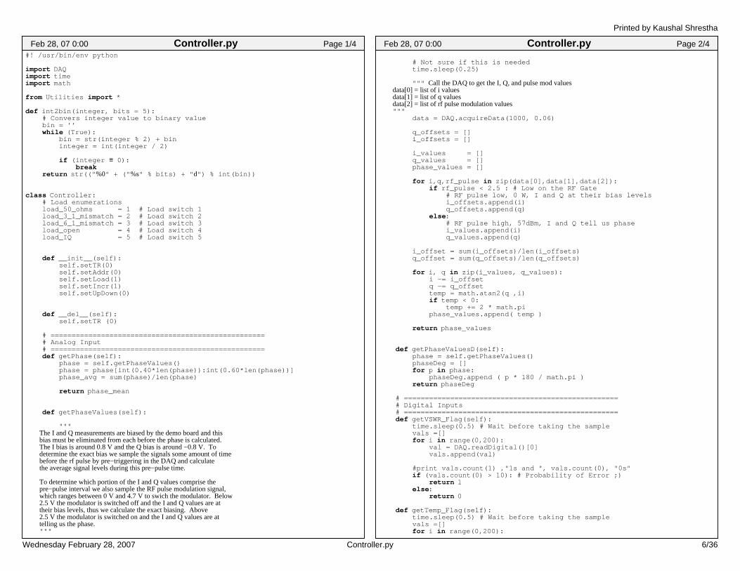
#! /usr/bin/env python
import DAQimport timeimport math
from Utilities import *
def int2bin(integer, bits = 5): # Convers integer value to binary value bin = ’’ while (True): bin = str(integer % 2) + bin integer = int(integer / 2) if (integer ≡ 0): break return str((" %0" + (" %s" % bits) + " d") % int(bin))
class Controller: # Load enumerations load_50_ohms = 1 # Load switch 1 load_3_1_mismatch = 2 # Load switch 2 load_6_1_mismatch = 3 # Load switch 3 load_open = 4 # Load switch 4 load_IQ = 5 # Load switch 5
def __init__(self): self.setTR(0) self.setAddr(0) self.setLoad(1) self.setIncr(1) self.setUpDown(0)
def __del__(self): self.setTR (0)
# =================================================== # Analog Input # =================================================== def getPhase(self): phase = self.getPhaseValues() phase = phase[int(0.40*len(phase)):int(0.60*len(phase))] phase_avg = sum(phase)/len(phase) return phase_mean
def getPhaseValues(self):
""" The I and Q measurements are biased by the demo board and this bias must be eliminated from each before the phase is calculated. The I bias is around 0.8 V and the Q bias is around −0.8 V. To determine the exact bias we sample the signals some amount of time before the rf pulse by pre−triggering in the DAQ and calculate the average signal levels during this pre−pulse time.
To determine which portion of the I and Q values comprise the pre−pulse interval we also sample the RF pulse modulation signal, which ranges between 0 V and 4.7 V to swich the modulator. Below 2.5 V the modulator is switched off and the I and Q values are at their bias levels, thus we calculate the exact biasing. Above 2.5 V the modulator is switched on and the I and Q values are at telling us the phase. """
Feb 28, 07 0:00 Page 1/4Controller.py
# Not sure if this is needed time.sleep(0.25)
""" Call the DAQ to get the I, Q, and pulse mod values data[0] = list of i values data[1] = list of q values data[2] = list of rf pulse modulation values """ data = DAQ.acquireData(1000, 0.06) q_offsets = [] i_offsets = []
i_values = [] q_values = [] phase_values = [] for i,q,rf_pulse in zip(data[0],data[1],data[2]): if rf_pulse < 2.5 : # Low on the RF Gate # RF pulse low, 0 W, I and Q at their bias levels i_offsets.append(i) q_offsets.append(q) else: # RF pulse high, 57dBm, I and Q tell us phase i_values.append(i) q_values.append(q)
i_offset = sum(i_offsets)/len(i_offsets) q_offset = sum(q_offsets)/len(q_offsets)
for i, q in zip(i_values, q_values): i −= i_offset q −= q_offset
temp = math.atan2(q ,i) if temp < 0: temp += 2 * math.pi
phase_values.append( temp )
return phase_values
def getPhaseValuesD(self): phase = self.getPhaseValues() phaseDeg = [] for p in phase: phaseDeg.append ( p * 180 / math.pi ) return phaseDeg # =================================================== # Digital Inputs # =================================================== def getVSWR_Flag(self): time.sleep(0.5) # Wait before taking the sample vals =[] for i in range(0,200): val = DAQ.readDigital()[0] vals.append(val)
#print vals.count(1) ,"1s and ", vals.count(0), "0s" if (vals.count(0) > 10): # Probability of Error ;) return 1 else: return 0
def getTemp_Flag(self): time.sleep(0.5) # Wait before taking the sample vals =[] for i in range(0,200):
Feb 28, 07 0:00 Page 2/4Controller.py
Printed by Kaushal Shrestha
Wednesday February 28, 2007 6/36Controller.py

val = DAQ.readDigital()[1] vals.append(val)
# print vals.count(1) ,"1s and ", vals.count(0), "0s" if (vals.count(0) > 10): # Probability of Error ;) return 1 else: return 0 # =================================================== # Digital Outputs # =================================================== def setAddr(self,addr): # Mask with 0000 0111 to ensure addr is from 000 − 111 addr = 0x07 & addr #print int2bin(addr, 3) DAQ.writeDigital(0, " 2:0", int2bin(addr, 3)) def setLoad(self,switchno = 1): # Switch can be from 1 to 5 self.setTR(0) # Makes sure of cold switching time.sleep(0.25) switchno = 1 << (switchno − 1) DAQ.writeDigital(0, " 7:3", int2bin(switchno, 5)) time.sleep(0.25) def setIncr(self,value): # Value takes in a 1 or a 0 # Incrementf.setIncr(1) is Bit number 3 in the 8 bit DIO if (bool(value) ≡ True): DAQ.writeDigital(1, " 6", " 1") else: DAQ.writeDigital(1, " 6", " 0")
def setUpDown(self,value): # Value takes in a 1 or a 0 # UpDown is Bit number 4 in the 8 bit DOUT if (bool(value) ≡ True): DAQ.writeDigital(1, " 7", " 1") else: DAQ.writeDigital(1, " 7", " 0")
def Increment(self,number_of_pulses=1): """ This function toggles setIncr a speified amount while self.setUpDown is set to one. number_of_pulses is the number of times you want the Incr Line to toggle from 1 to 0 """ self.setUpDown(1) timedelay = 0.0625 time.sleep(timedelay) self.setIncr(1) for i in range(0,2*number_of_pulses): self.setIncr(i % 2) time.sleep(2e−6) self.setIncr(1) time.sleep(timedelay)
def Decrement(self,number_of_pulses=1): """ This function toggles setIncr a specified amount while self.setUpDown is set to zero.
number_of_pulses is the number of times you want the Incr Line to toggle from 1 to 0 """
Feb 28, 07 0:00 Page 3/4Controller.py self.setUpDown(0) timedelay = 0.0625 time.sleep(timedelay) self.setIncr(1) for i in range(0,2*number_of_pulses): self.setIncr(i % 2) time.sleep(2e−6) self.setIncr(1) time.sleep(timedelay)
# =================================================== # Timers (Gating Signals) # =================================================== def setTR(self, val, period = 20e−3, pw = 2e−3): if val ≡ 0: DAQ.stopTimers() elif val ≡ 1: DAQ.loadTimers(0,period,pw) def setRF(self, val, period = 20e−3, pw = 2e−3): # 10 % duty cycle if val ≡0: DAQ.stopTimers() #DAQ.loadTimers(0,period,pw) elif val ≡ 1: DAQ.loadTimers(1,period,pw)
def setRFHigh(self): self.setTR(0) DAQ.writeDigital( 2 , # port " 4", # lines " 1" ) # value def setRFLow(self): DAQ.writeDigital(2, " 4", " 0")
Feb 28, 07 0:00 Page 4/4Controller.py
Printed by Kaushal Shrestha
Wednesday February 28, 2007 7/36Controller.py

#!/usr/bin/env python
import sysimport stringimport datetimeimport pytzimport psycopg2
# load the psycopg extras moduleimport psycopg2.extras
UTC = pytz.timezone( ’ UTC’ )
class Database: def __init__(self): self.dbcon = self.connect()
def connect(self): dbcon = None try: dbhost = None # None or hostname dbname = " sspa" # Database name dbuser = None # "postgres"
if dbhost: # if host is given then auth mechanism is different connect_string = ’ host=%s dbname=%s user=%s’ % \ ( dbhost, dbname, dbuser ) else: if dbuser: connect_string = ’ dbname=%s user=%s’ % \ ( dbname, dbuser ) else: connect_string = ’ dbname=%s’ % \ ( dbname ) dbcon = psycopg2.connect( connect_string ) except psycopg2.OperationalError, inst: msg = " %s db dbcon failed: %s"% (__name__,inst) print msg raise return dbcon
def storeCalibrationReadings(self, names_str, values_str): names_str = names_str + ’ , dt’ values_str = values_str + " , ’%s’" % datetime.datetime.utcnow() self.insertTuples( " calibration", names_str, values_str)
def storeOvenTestReadings(self, names_str, values_str): names_str = names_str + ’ , dt’ values_str = values_str + " , ’%s’" % datetime.datetime.utcnow() self.insertTuples( " oventest", names_str, values_str )
def storePreBurninReadings(self, names_str, values_str): names_str = names_str + ’ , dt’ values_str = values_str + " , ’%s’" % datetime.datetime.utcnow() self.insertTuples( " preburnin", names_str, values_str ) def storePostBurninReadings(self, names_str, values_str): names_str = names_str + ’ , dt’ values_str = values_str + " , ’%s’" % datetime.datetime.utcnow() self.insertTuples( " postburnin", names_str, values_str ) def storeDVTReadings(self, names_str, values_str, tablename): names_str = names_str + ’ , dt’ values_str = values_str + " , ’%s’" % datetime.datetime.utcnow() self.insertTuples( tablename, names_str, values_str )
Feb 28, 07 0:03 Page 1/2Database.py def storeOffsetSettings(self, names_str, values_str): names_str = names_str + ’ , dt’ values_str = values_str + " , ’%s’" % datetime.datetime.utcnow() self.insertTuples( " offset_calibration", names_str, values_str ) def insertTuples( self, tablename, names_str, values_str ): dbcur = self.dbcon.cursor() strSQL = " INSERT INTO %s (%s) VALUES (%s)" % \ ( tablename, names_str, values_str ) try: dbcur.execute(strSQL) except psycopg2.ProgrammingError, e: msg = " ProgrammingError: %s" % e print msg self.dbcon.rollback() raise
try: self.dbcon.commit() except psycopg2.ProgrammingError, e: msg = " ProgrammingError %s, not committing" % e print msg self.dbcon.rollback() raise dbcur.close()
if __name__ ≡ " __main__": db=Database() for i in db.fetchData(): print i
Feb 28, 07 0:03 Page 2/2Database.py
Printed by Kaushal Shrestha
Wednesday February 28, 2007 8/36Database.py
#!/usr/bin/env python
import DVTTestsimport OperationalTest
import stringimport osimport sysimport time
from TestException import *from Utilities import *
class DVT: def __init__(self): os.system(’ reset’) self.WelcomeScreen()
def WelcomeScreen(self): os.system(’ clear’) setStyle(’ bold’) print 60 * " =" print " Welcome to the AMISR SSPA Design Verification Test Suite" print 60 * " =" setStyle(’ default’)
def Login(self): print "" print " Please login below (avoid spaces) ... " LoginName = "" while LoginName ≡ "": try: LoginName = str(raw_input(" Username : ")) LoginName = LoginName.strip().replace(" "," _") except KeyboardInterrupt: print " \n" setStyle(’ default’) sys.exit(1) self.UserName = LoginName
def run (self): while True: self.Login() self.WelcomeScreen() while ¬ (self.UserName ≡ ""): print "" print " 0. Log Off", self.UserName print " 1. Qualification Test" # Pre−burnin print " 2. Operational Test" # Oventest print " 3. Pre−test Benchmark" # Pre−burnin print " 4. Post−test Benchmark" # Post−burnin print " Q. Quit\n"
inp = "" while inp ≡ "": try: inp = raw_input(" Enter our choice : ") inp = string.lower( str(inp) ) inp = inp.strip() except KeyboardInterrupt: setStyle( ’ bold’, ’ red’ ) print " \n\nForced Termination By the User ... \n" setStyle( ’ default’ ) sys.exit(1) if ( inp ≡ " q" ): return
Feb 27, 07 23:53 Page 1/2DVT.py elif ( inp ≡ " 0" ): self.UserName = "" break try: # Try .. Finaly block try: # Try .. Except block if ( inp ≡ " 1" ): proc = DVTTests.DVTTests(self.UserName) proc.runDVT( proc.qualification_test ) elif ( inp ≡ " 2" ): proc = OperationalTest.OperationalTest \ (self.UserName) proc.runOperationalTest() elif ( inp ≡ " 3" ): proc = DVTTests.DVTTests(self.UserName) proc.runDVT( proc.pretest_benchmark ) elif ( inp ≡ " 4" ): proc = DVTTests.DVTTests(self.UserName) proc.runDVT( proc.posttest_benchmark ) except KeyboardInterrupt: setStyle( ’ bold’, ’ red’ ) print " \n\nProcess Terminated By User ... \n" setStyle( ’ default’ ) except Exception, err: setStyle(’ bold’, ’ red’) print " \n", 65 * " −" msg = err.__str__().split(" \n") for _msg in msg: print ’ ’ + _msg print 65 * " −" setStyle( ’ default’ ) finally: # Delete the object so that it calls its destructor # to restore settings to default try: proc.destructor()
del proc except:
pass if __name__ ≡ " __main__": DVT().run() print " \nPlease wait while the system shuts down ... \n\n"
Feb 27, 07 23:53 Page 2/2DVT.py
Printed by Kaushal Shrestha
Wednesday February 28, 2007 9/36DVT.py

#! /usr/bin/env python
import SpecTestsimport Database
import timeimport stringimport sysimport math
from TestException import *from Utilities import *
###################################################################### Specifications Tests for Design Verification Test####################################################################
class DVTTests: qualification_test = 1 pretest_benchmark = 2 posttest_benchmark = 3
dict_tests = qualification_test : " Qualification Test", pretest_benchmark : " Pre−test Benchmark", posttest_benchmark : " Post−test Benchmark"
def __init__(self, username): try: self.spectest = SpecTests.SpecTests(username) self.user = username except Exception: raise def __del__(self): try: del self.spectest except: pass
# ******************************************************************** # # Start of "Public Functions" Block # # ********************************************************************
# ==================================================================== """ Qualification Test / Pre−test Benchmark / Post−test Benchmark
1. OverPulse Test 2. Droop Test 3. Power Efficiency Test 4. Power Correct Test 5. Open Load Test 6. Mismatch Load Test """ def runDVT(self, testType ): values = " sn" : " ", " uname" : " ", " pulsewidth" : " ", " overpulse_passed" : " ", " droop_initpower" : " ",
Feb 26, 07 14:50 Page 1/4DVTTests.py " droop_finalpower" : " ", " droop_passed" : " ",
" current_430" : " ", " voltage_430" : " ", " power_430" : " ",
" current_450" : " ", " voltage_450" : " ", " power_450" : " ",
" current_440" : " ", " voltage_440" : " ", " power_440" : " ",
" power_8_5" : " ", " power_11_5" : " ", " powercorrect_passed": " ",
" open_passed" : " ", " mismatch_passed" : " " # Values dictionary
testFailFlag = False serialno = "" while serialno ≡ "": print "" sn = raw_input(" Please enter the Serial Number of the SSPA :") serialno = str(sn).strip().replace(" "," _")
values[’ sn’] = " ’%s’" % serialno values[’ uname’] = " ’%s’" % self.user
setStyle( ’ bold’, ’ white’ ) print " \nInitializing %s Test Porcedures..." % \ self.dict_tests[ testType ] setStyle( ’ default’ )
# Initialize devices self.spectest.initDevices()
# Overpulse with 3ms pulse overpulse = self.conductOverPulseTest() values [ ’ pulsewidth’ ] = " ’%s’" % string.join(overpulse[0], " ,") values [ ’ overpulse_passed’ ] = " ’%s’" % str( ¬ bool(overpulse[1])) if bool(overpulse[1]) ≡ True: # Returns fail code as 1 if fails testFailFlag = True # Droop (droop, droop_passed) = self.conductDroopTest() values [ ’ droop_initpower’ ] = " ’%s’" % droop[0] values [ ’ droop_finalpower’ ] = " ’%s’" % droop[1] values [ ’ droop_passed’ ] = " ’%s’" % droop_passed if droop_passed ≡ False: testFailFlag = True # Efficiency at 430, 440, 450 (currents, voltages, powers, failflag) = self.conductEfficiencyTest() for i in [430,440,450]: # index 0,1,2 given by i /10 − 43 values [ " current_%s" % i ] = " ’%s’" % currents [i/10 − 43] values [ " voltage_%s" % i ] = " ’%s’" % voltages [i/10 − 43] values [ " power_%s" % i ] = " ’%s’" % powers [i/10 − 43]
testFailFlag = failflag sys.stdout.write ( " Efficiency Test after burnin ...\t" ) if ( failflag ≡ False ): # Passed setStyle(’ bold’, ’ green’ ) sys.stdout.write(" [ PASSED ]")
Feb 26, 07 14:50 Page 2/4DVTTests.py
Printed by Kaushal Shrestha
Wednesday February 28, 2007 10/36DVTTests.py

setStyle(’ default’) else: # Failed setStyle(’ bold’, ’ red’ ) sys.stdout.write(" [ FAILED ]") setStyle(’ default’) # Power Correct powercorrect = self.conductPowerCorrectTest() values [ ’ power_8_5’ ] = powercorrect[0][0] values [ ’ power_11_5’] = powercorrect[0][1] values [ ’ powercorrect_passed’ ] = " ’%s’" % \ str( ¬ bool(powercorrect[1])) if bool(powercorrect[1]) ≡ True: testFailFlag = True # Open and Mismatch variousloads_passed = self.conductVariousLoadsTest() values [ ’ open_passed’ ] = " ’%s’" % \ str(bool(variousloads_passed[0])) values [ ’ mismatch_passed’ ] = " ’%s’" % \ str(bool(variousloads_passed[1])) if bool(variousloads_passed[0]) ≡ False ∨ \ bool(variousloads_passed[1]) ≡ False: testFailFlag = True # Save Data # −−−−−−−−−−−−−−−−−−−−−−−−−−−−−−−−−−−−−−−−− self.__saveResults(values, testType) # −−−−−−−−−−−−−−−−−−−−−−−−−−−−−−−−−−−−−−−−− # ========================================= # End of Procedure print " \n" if testFailFlag ≡ True: setStyle(’ bold’, ’ red’) print 35 * ’ −’ print " %s Failed !!!" % self.dict_tests[ testType ] print 35 * ’ −’ else: setStyle(’ bold’, ’ green’) print 35 * ’ −’ print " %s Completed !!!" % self.dict_tests[ testType ] print 35 * ’ −’
setStyle(’ default’) # ==================================================================
############################################################ ## Data Saving Routines ############################################################ def __saveResults(self, results, testType): tablename = self.qualification_test : " dvt_qualification", self.pretest_benchmark : " dvt_pretest_benchmark", self.posttest_benchmark : " dvt_posttest_benchmark" names = [ ] values = [ ] for fieldname, value in results.items(): names.append( " %s" % fieldname ) values.append( " %s" % value ) names_str = string.join(names, ’ , ’) values_str = string.join(values, ’ , ’) db = Database.Database() db.storeDVTReadings(names_str, values_str, tablename[testType])
Feb 26, 07 14:50 Page 3/4DVTTests.py
# ******************************************************************** # End of Private Functions Block # ********************************************************************
Feb 26, 07 14:50 Page 4/4DVTTests.py
Printed by Kaushal Shrestha
Wednesday February 28, 2007 11/36DVTTests.py

#! /usr/bin/env python# −*− python −*−
from Tkinter import *import Tkinter as Tkimport Controller
#################################################### Manual Control Functions ##################################################
def setLoadOne(event): selectRFandGateOff() controller.setLoad(controller.load_50_ohms) print " load switched to one" def setLoadTwo(event): selectRFandGateOff() controller.setLoad(controller.load_6_1_mismatch) print " load switched to two" def setLoadFive(event): selectRFandGateOff() controller.setLoad(controller.load_IQ) print " load switched to five" def setLoadFour(event): selectRFandGateOff() controller.setLoad(controller.load_open) print " load switched to four"
def setLoadThree(event): selectRFandGateOff() controller.setLoad(controller.load_3_1_mismatch) print " load switched to three" def setRFandGateOff(event): controller.setTR(0) print " Both Off"
def setGateOn(event): controller.setTR(1) print " Gate Only"
def setRFandGateOn(event): controller.setRF(1) print " RF and Gate On"
def selectRFandGateOff(): SELF.frame2_RFandGateOff.select()
def exitWindow(event=None): setRFandGateOff(None) setLoadOne(None) #root1.iconify() root2.destroy()
class manualControlsInterface: def __init__(self, master): #, main1, timeVar, loadVar, master=None): global root2 global SELF global controller
global load global timevar
Feb 28, 07 8:14 Page 1/3guiManualControls.py
SELF = self root2 = master controller = Controller.Controller() timevar = StringVar() load = StringVar()
root2.protocol(" WM_DELETE_WINDOW", exitWindow)
frame1 = Frame(root2, width=" 325", height=" 215", relief=" groove", borderwidth=" 2") frame1.place(in_=root2, x=10, y=10)
frame2 = Frame(root2, width=" 325", height=" 215", relief=" groove", borderwidth=" 2") frame2.place(in_=root2, x=340, y=10)
frame3 = Frame(root2, width=" 655", height=" 35", relief=" groove", borderwidth=" 2") frame3.place(in_=root2, x=10, y=235)
self.frame2_timercardHeading = Label (frame2, text=" Gating Line Settings", font=" Helvetica 14 bold") self.frame2_timercardHeading.place(in_= frame2,x=70,y=10)
self.frame2_RFandGateOff = Radiobutton (frame2, text=" RF and Gate OFF", variable=timevar, value=1, cursor=" hand2") self.frame2_RFandGateOff.place(in_=frame2,x=70,y=80) self.frame2_RFandGateOff.bind(" <Button−1>", func=setRFandGateOff) self.frame2_RFandGateOff.select() setRFandGateOn(None)
self.frame2_GateOn = Radiobutton (frame2, text=" Gate ON", variable=timevar, value=2, cursor=" hand2") self.frame2_GateOn.place(in_=frame2,x=70,y=110) self.frame2_GateOn.bind(" <Button−1>", func=setGateOn)
self.frame2_RFandGateOn = Radiobutton (frame2, text=" RF and Gate ON", variable=timevar, value=3, cursor=" hand2") self.frame2_RFandGateOn.place(in_=frame2,x=70,y=140) self.frame2_RFandGateOn.bind(" <Button−1>", func=setRFandGateOn)
self.frame1_switchHeading = Label (frame1, text=" Load Switch Settings", font=" Helvetica 14 bold") self.frame1_switchHeading.place(in_=frame1,x=40,y=10) self.frame1_loadOne = Radiobutton(frame1, text=" 50 Ohm", variable=load, value=1, cursor=" hand2") self.frame1_loadOne.place(in_=frame1,x=50,y=60) self.frame1_loadOne.bind(" <Button−1>", func=setLoadOne) self.frame1_loadOne.select() setLoadOne(None)
self.frame1_loadTwo = Radiobutton(frame1, text=" 6:1 Mismatch", variable=load, value=2, cursor=" hand2") self.frame1_loadTwo.place(in_=frame1,x=50,y=90) self.frame1_loadTwo.bind(" <Button−1>", func=setLoadTwo)
self.frame1_loadThree = Radiobutton(frame1, text=" 3:1 Mismatch", variable=load, value=3, cursor=" hand2")
Feb 28, 07 8:14 Page 2/3guiManualControls.py
Printed by Kaushal Shrestha
Wednesday February 28, 2007 12/36guiManualControls.py
self.frame1_loadThree.place(in_=frame1,x=50,y=120) self.frame1_loadThree.bind(" <Button−1>", func=setLoadThree)
self.frame1_loadFour = Radiobutton(frame1, text=" Open", variable=load, value=4, cursor=" hand2") self.frame1_loadFour.place(in_=frame1,x=50,y=150) self.frame1_loadFour.bind(" <Button−1>", func=setLoadFour)
self.frame1_loadFive = Radiobutton(frame1, text=" IQ Detector", variable=load, value=5, cursor=" hand2") self.frame1_loadFive.place(in_=frame1,x=50,y=180) self.frame1_loadFive.bind(" <Button−1>", func=setLoadFive) self.frame3_backButton = Button(frame3, text=" Quit", cursor=" hand2") self.frame3_backButton.place(in_=frame3, x=575, y=0) self.frame3_backButton.bind(" <Button−1>", func=exitWindow)
if __name__ ≡ " __main__": root = Tk.Tk() root.resizable(0,0) root.title(’ Welcome to the Automated Test Suite (ATS)’)
# Center the window in the the display screen w , h = 675, 275 ws, hs = root.winfo_screenwidth(), root.winfo_screenheight() x , y = (ws/2) − (w/2), (hs/2) − (h/2) root.geometry(’ %dx%d+%d+%d’ % (w, h, x, y)) w = manualControlsInterface (root) root.mainloop()
Feb 28, 07 8:14 Page 3/3guiManualControls.py
Printed by Kaushal Shrestha
Wednesday February 28, 2007 13/36guiManualControls.py

#! /usr/bin/env python
import Controllerimport PowerMeterimport SignalGenimport Database
import mathimport timeimport stringimport sysimport os
from TestException import *
offset1_ref = 2.3 # signal generator dBmoffset1_tol = 0.5 # plus/minus 0.5 dB
offset2_ref = 20 # input power dBmoffset2_tol = 1 # plus/minus 1 dB
offset3_ref = 59 # output poweroffset3_tol = 1 # plus/minus 1 dB
class OffsetCalibration: def __init__(self): try: # Resetting offsets values in the offsets.ini file self.__writeOffsets (0,0,0) print " \nInitializing Devices..." self.powermeter = PowerMeter.PowerMeter( True ) # True to allow offsets.ini not found condition # Zeroing takes time, so the function has time.sleep(3) self.powermeter.zeroPowerHeads()
self.siggen = SignalGen.SignalGen( True ) # True to allow offsets.ini not found condition self.controller = Controller.Controller() except TestException: raise
def destructor(self): try: del self.powermeter del self.siggen del self.controller except: pass
# ****************************************************************** # # Public Functions Block # # ****************************************************************** def CalibrateOffset(self): # print "\n\nWelcome to the Offset Calibration Wizard." # print "If you have an SSPA connected, please disconnect it !!!" inp = " n" while ¬ ( inp ≡ " y" ∨ inp ≡ " q" ): print " \nStep 1: Connect ’Amp Input’ to ’CABLE B’" print " \tusing the N−Type to SMA adapter provided..." inp = string.lower(raw_input(" Did you do this? [y/q]: ")) if inp ≡ " q": raise TestException (TestException.process_abort_offsetcalib)
print " \nTurning on RF, Please wait ...\n"
Feb 27, 07 23:51 Page 1/3OffsetCalibration.py self.controller.setRFHigh() # Sets pulse mod to high, i.e., on
# initialize out of bounds to ensure measurement and adjustment power = 999 self.siggen.setAmplitude(10) offset1 = 0 self.siggen.setRFOn() power = self.powermeter.getMeasOutput( offsetcalibration = True )
print " Power reading : %s dBm (without offset compensation)" % power target_power_at_sspa_input = 10 offset1 = target_power_at_sspa_input − power print " Calculated offset for Signal generator: %s dB" % offset1
# Sanity check for offset 1 if offset1 < (offset1_ref − offset1_tol) ∨ \ offset1 > (offset1_ref + offset1_tol): print " Signal generator offset:" print " \tExpected : %s, plus/minus %s dB \t Calculated : %s dB" % \ (offset1_ref, offset1_tol, offset1) self.__saveResults( offset1) raise TestException (TestException.calib_offsetCalibfailed)
self.siggen.setAmplitude(target_power_at_sspa_input + offset1)
power = self.powermeter.getMeasOutput( True ) print " Power reading : %s dBm (with offset compensation)" % (power) chAReading = self.powermeter.getMeasInput( offsetcalibration = True ) print " \nCorresponding reading in Channel A is %s dBm" % chAReading offset2 = target_power_at_sspa_input − chAReading print " Calculated Offset for Channel A is %s dB" % offset2
# Sanity check for offset 2 if offset2 < (offset2_ref − offset2_tol) ∨ \ offset2 > (offset2_ref + offset2_tol): print " Input Power offset:" print " \tExpected : %s, plus/minus %s dB \t Calculated : %s dB" % \ (offset2_ref, offset2_tol, offset2) self.__saveResults( offset1, offset2) raise TestException (TestException.calib_offsetCalibfailed)
self.siggen.setRFOff() self.siggen.setAmplitude(17) # dBm self.siggen.setRFOn() fullpower = self.powermeter.getMeasOutput(1) self.siggen.setRFOff()
inp = " n" while ¬ ( inp ≡ " y" ∨ inp ≡ " q" ): print " \nStep 2: Now connect Cable B back to Channel B."
inp = string.lower(raw_input(" Did you do this? [y/q]: ")) if inp ≡ " q": raise TestException (TestException.process_abort_offsetcalib)
while True: inp = " n" while ¬ ( inp ≡ " y" ∨ inp ≡ " q" ): print " \nStep 3: Connect ’Amp Input’ to ’Amp Output’" print " \tusing the N−Type to SMA adapter provided." inp = string.lower(raw_input(" Did you do this? [y/q]: ")) if inp ≡ " q": raise TestException \ (TestException.process_abort_offsetcalib) self.siggen.setRFOn() time.sleep( 2 )
Feb 27, 07 23:51 Page 2/3OffsetCalibration.py
Printed by Kaushal Shrestha
Wednesday February 28, 2007 14/36OffsetCalibration.py

chBReading = self.powermeter.getMeasOutput(1) print " Corresponding reading in Channel B is %s dBm" % chBReading offset3 = (fullpower) − chBReading print " Offset for Channel B is %s dB" % offset3
# Sanity check for offset 3 if offset3 < (offset3_ref − offset3_tol) ∨ \ offset3 > (offset3_ref + offset3_tol): print " Output Power offset:" print " \tExpected: %s, plus/minus %s dB \t Calculated: %s dB" \ % (offset3_ref, offset3_tol, offset3) inp = "" while ( inp ≠ " y" ∧ inp ≠ " n"): inp = raw_input(" Do you want to redo this step? [y/n]") inp = string.lower(str(inp)) if inp ≡ " y": continue elif inp ≡ " n": self.__saveResults( offset1, offset2, offset3 ) raise TestException (TestException.calib_offsetCalibfailed) break # Break While if it passes successfully
self.__writeOffsets(offset1, offset2, offset3) self.__saveResults(offset1, offset2, offset3); self.siggen.setRFOff() self.controller.setRFLow() print " \nOffset Calibration Complete!" return 1
# ****************************************************************** # # Private Functions Block # # ****************************************************************** def __writeOffsets(self,siggen, input, output): #Writes the offsets to offsets.ini import pytz import datetime UTC = pytz.timezone(’ UTC’) mytz = pytz.timezone(’ America/Los_Angeles’) my_time = datetime.datetime.utcnow().replace(tzinfo = UTC) f = open( os.environ[ ’ HOME’ ] + ’ /Code/offsets.ini’, ’ w’) f.write(" This file contains the offset due to losses and attn in dB.") f.write(" \nInput Offset : %s" % input ) f.write(" \nOutput Offset : %s" % output ) f.write(" \nSig Gen Offset: %s" % siggen ) f.write(" \nDate and Time Stamp : %s" % my_time.astimezone(mytz)) f.close()
def __saveResults(self, offset_1, offset_2 = ’ NULL ’, offset_3 =’ NULL ’): offsets = [ offset_1, offset_2, offset_3 ] names = [ ] values = [ ] cnt = 1 for i in offsets: names.append ( " offset_%s" % cnt ) values.append( " %s" % i) cnt += 1
names_str = string.join(names, ’ , ’) values_str = string.join(values, ’ , ’) db = Database.Database() db.storeOffsetSettings (names_str, values_str)
Feb 27, 07 23:51 Page 3/3OffsetCalibration.py
Printed by Kaushal Shrestha
Wednesday February 28, 2007 15/36OffsetCalibration.py
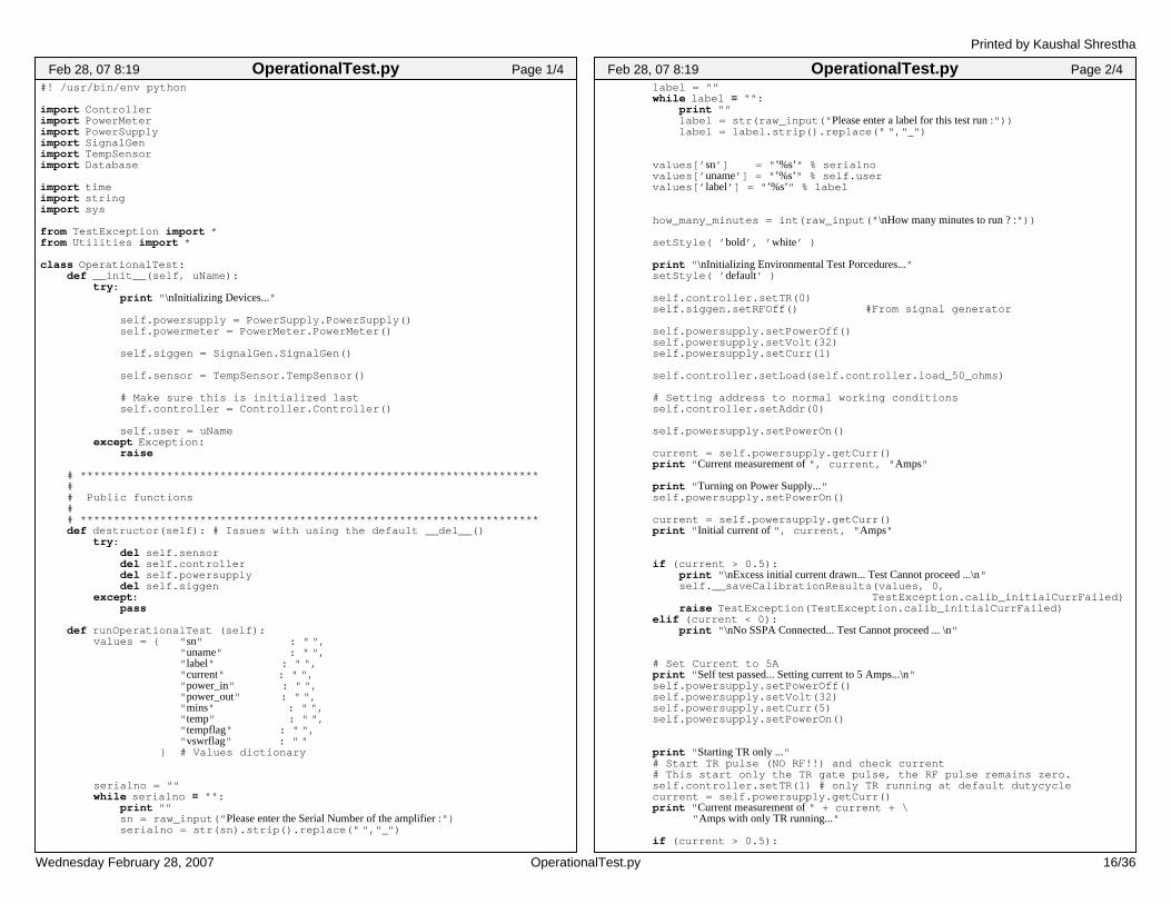
#! /usr/bin/env python
import Controllerimport PowerMeterimport PowerSupplyimport SignalGenimport TempSensorimport Database
import timeimport stringimport sys
from TestException import *from Utilities import *
class OperationalTest: def __init__(self, uName): try: print " \nInitializing Devices..." self.powersupply = PowerSupply.PowerSupply() self.powermeter = PowerMeter.PowerMeter()
self.siggen = SignalGen.SignalGen()
self.sensor = TempSensor.TempSensor() # Make sure this is initialized last self.controller = Controller.Controller() self.user = uName except Exception: raise # ********************************************************************* # # Public functions # # ********************************************************************* def destructor(self): # Issues with using the default __del__() try:
del self.sensor del self.controller del self.powersupply del self.siggen except: pass
def runOperationalTest (self): values = " sn" : " ", " uname" : " ", " label" : " ", " current" : " ", " power_in" : " ", " power_out" : " ", " mins" : " ", " temp" : " ", " tempflag" : " ", " vswrflag" : " " # Values dictionary
serialno = "" while serialno ≡ "": print "" sn = raw_input(" Please enter the Serial Number of the amplifier :") serialno = str(sn).strip().replace(" "," _")
Feb 28, 07 8:19 Page 1/4OperationalTest.py label = "" while label ≡ "": print "" label = str(raw_input(" Please enter a label for this test run :")) label = label.strip().replace(" "," _")
values[’ sn’] = " ’%s’" % serialno values[’ uname’] = " ’%s’" % self.user values[’ label’] = " ’%s’" % label
how_many_minutes = int(raw_input(" \nHow many minutes to run ? :"))
setStyle( ’ bold’, ’ white’ )
print " \nInitializing Environmental Test Porcedures..." setStyle( ’ default’ )
self.controller.setTR(0) self.siggen.setRFOff() #From signal generator self.powersupply.setPowerOff() self.powersupply.setVolt(32) self.powersupply.setCurr(1)
self.controller.setLoad(self.controller.load_50_ohms)
# Setting address to normal working conditions self.controller.setAddr(0)
self.powersupply.setPowerOn()
current = self.powersupply.getCurr() print " Current measurement of ", current, " Amps"
print " Turning on Power Supply..." self.powersupply.setPowerOn()
current = self.powersupply.getCurr() print " Initial current of ", current, " Amps"
if (current > 0.5): print " \nExcess initial current drawn... Test Cannot proceed ...\n" self.__saveCalibrationResults(values, 0, TestException.calib_initialCurrFailed) raise TestException(TestException.calib_initialCurrFailed) elif (current < 0): print " \nNo SSPA Connected... Test Cannot proceed ... \n" # Set Current to 5A print " Self test passed... Setting current to 5 Amps...\n" self.powersupply.setPowerOff() self.powersupply.setVolt(32) self.powersupply.setCurr(5) self.powersupply.setPowerOn()
print " Starting TR only ..." # Start TR pulse (NO RF!!) and check current # This start only the TR gate pulse, the RF pulse remains zero. self.controller.setTR(1) # only TR running at default dutycycle current = self.powersupply.getCurr() print " Current measurement of " + current + \ " Amps with only TR running..."
if (current > 0.5):
Feb 28, 07 8:19 Page 2/4OperationalTest.py
Printed by Kaushal Shrestha
Wednesday February 28, 2007 16/36OperationalTest.py

print " \nToo much current drawn when turning on TR only..." + \ " Test Cannot proceed ...\n" return self.__saveCalibrationResults(values, \ 0, TestException.calib_gatePulseFailed) raise TestException(TestException.calib_gatePulseFailed)
print " Waiting for RF to turn on" time.sleep(2) # Start RF signal self.siggen.setRFOn()
# Start RF Input and TR gating print " Turning RF gate on...\n" self.controller.setRF(1) # RF and TR running at default values time.sleep(5) # Time delay before starting to measure current
minutes = 0 while True: sys.stdout.write( " \nAcquring Data ... \t\t" ) sys.stdout.flush() current = self.powersupply.getCurr() powerin = self.powermeter.getMeasInput() powerout = self.powermeter.getMeasOutput()
values[’ current’] = (" %s" % current) values[’ power_in’] = (" %s" % powerin) values[’ power_out’]= (" %s" % powerout) values[’ mins’] = minutes values[’ temp’] = self.sensor.getTemperature() values[’ tempflag’] = (" ’%s’" % self.controller.getTemp_Flag()) values[’ vswrflag’] = (" ’%s’" % self.controller.getVSWR_Flag()) sys.stdout.write( " \nSaving Data ...\n" ) sys.stdout.flush() print " Power in :%s, Power out :%s, Current :%s" % \ (powerin, powerout, current)
# Database save call self.__saveOvenTestResults(values)
# Check for break condition if minutes ≥ how_many_minutes: break # Go back to the loop seconds = 0 while seconds < 60: str_time = str(minutes) + ’ minutes and ’ + str(seconds) + \ ’ seconds...’ sys.stdout.write( " \rWaiting:%s" % str_time ) sys.stdout.flush() time.sleep(1) seconds += 1 minutes += 1 # ========================================= # End of Oven Test Procedure print "" setStyle(’ bold’, ’ green’) print 35 * ’ −’ print " Oven Test Completed !!!" print 35 * ’ −’ setStyle(’ default’) # ========================================= # *********************************************************************
Feb 28, 07 8:19 Page 3/4OperationalTest.py # # Private functions # # ********************************************************************* def __saveOvenTestResults(self, results, teststatus=1, failcode=’ NULL ’): # By default the test passes and the fail code is ’NULL’
names = [ ] values = [ ] for fieldname, value in results.items(): names.append( " %s" % fieldname ) values.append( " %s" % value ) names_str = string.join(names, ’ , ’) values_str = string.join(values, ’ , ’) db = Database.Database() db.storeOvenTestReadings(names_str, values_str)
if __name__ ≡ ’ __main__’: OvenTest(" kaushal").OvenTest()
Feb 28, 07 8:19 Page 4/4OperationalTest.py
Printed by Kaushal Shrestha
Wednesday February 28, 2007 17/36OperationalTest.py
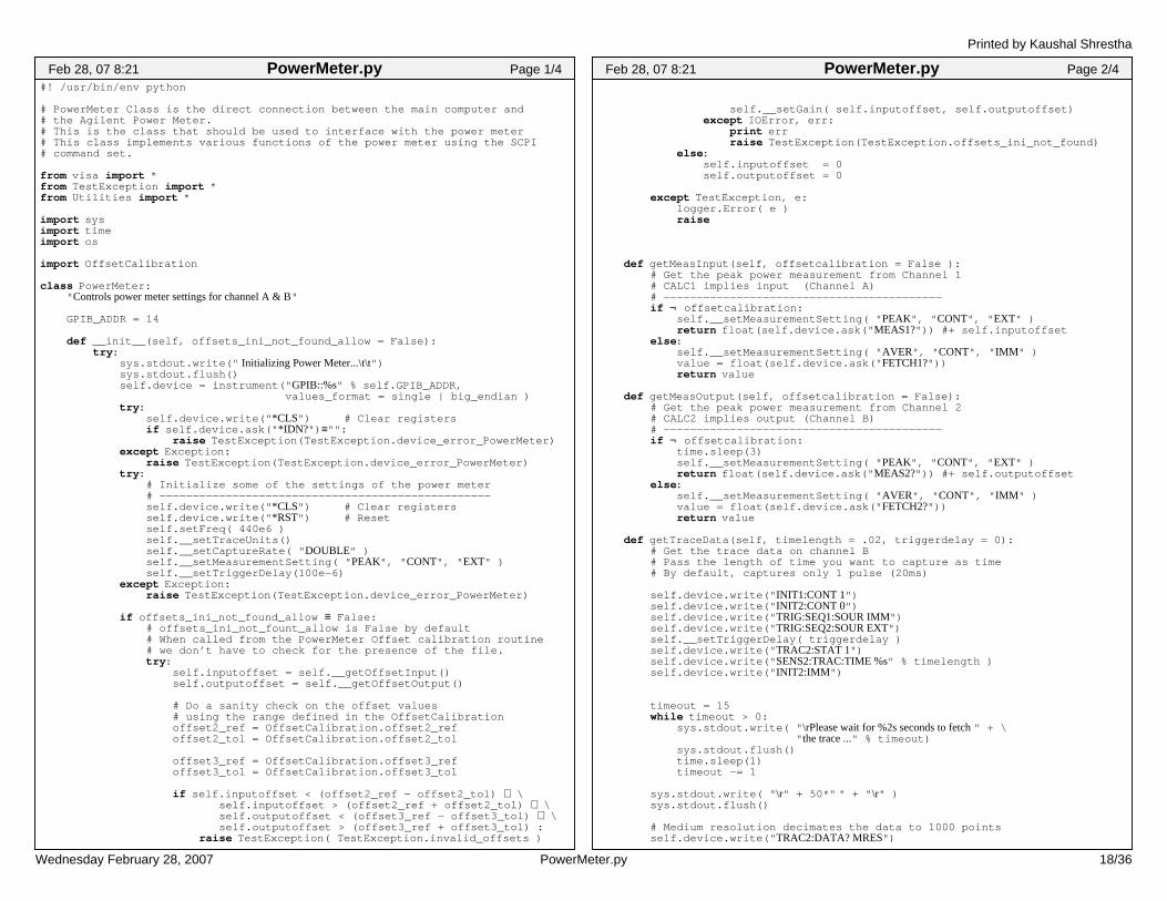
#! /usr/bin/env python
# PowerMeter Class is the direct connection between the main computer and# the Agilent Power Meter.# This is the class that should be used to interface with the power meter# This class implements various functions of the power meter using the SCPI# command set.
from visa import *from TestException import *from Utilities import *
import sysimport timeimport os
import OffsetCalibration
class PowerMeter: " Controls power meter settings for channel A & B"
GPIB_ADDR = 14 def __init__(self, offsets_ini_not_found_allow = False): try: sys.stdout.write(" Initializing Power Meter...\t\t") sys.stdout.flush() self.device = instrument(" GPIB::%s" % self.GPIB_ADDR, values_format = single | big_endian ) try: self.device.write(" *CLS") # Clear registers if self.device.ask(" *IDN?") ≡"": raise TestException(TestException.device_error_PowerMeter) except Exception: raise TestException(TestException.device_error_PowerMeter) try: # Initialize some of the settings of the power meter # −−−−−−−−−−−−−−−−−−−−−−−−−−−−−−−−−−−−−−−−−−−−−−−−−− self.device.write(" *CLS") # Clear registers self.device.write(" *RST") # Reset self.setFreq( 440e6 ) self.__setTraceUnits() self.__setCaptureRate( " DOUBLE" ) self.__setMeasurementSetting( " PEAK", " CONT", " EXT" ) self.__setTriggerDelay(100e−6) except Exception: raise TestException(TestException.device_error_PowerMeter)
if offsets_ini_not_found_allow ≡ False: # offsets_ini_not_fount_allow is False by default # When called from the PowerMeter Offset calibration routine # we don’t have to check for the presence of the file. try: self.inputoffset = self.__getOffsetInput() self.outputoffset = self.__getOffsetOutput()
# Do a sanity check on the offset values # using the range defined in the OffsetCalibration offset2_ref = OffsetCalibration.offset2_ref offset2_tol = OffsetCalibration.offset2_tol
offset3_ref = OffsetCalibration.offset3_ref offset3_tol = OffsetCalibration.offset3_tol if self.inputoffset < (offset2_ref − offset2_tol) ∨ \ self.inputoffset > (offset2_ref + offset2_tol) ∨ \ self.outputoffset < (offset3_ref − offset3_tol) ∨ \ self.outputoffset > (offset3_ref + offset3_tol) : raise TestException( TestException.invalid_offsets )
Feb 28, 07 8:21 Page 1/4PowerMeter.py
self.__setGain( self.inputoffset, self.outputoffset) except IOError, err: print err raise TestException(TestException.offsets_ini_not_found) else: self.inputoffset = 0 self.outputoffset = 0
except TestException, e: logger.Error( e ) raise
def getMeasInput(self, offsetcalibration = False ):
# Get the peak power measurement from Channel 1# CALC1 implies input (Channel A)# −−−−−−−−−−−−−−−−−−−−−−−−−−−−−−−−−−−−−−−−−−
if ¬ offsetcalibration: self.__setMeasurementSetting( " PEAK", " CONT", " EXT" ) return float(self.device.ask(" MEAS1?")) #+ self.inputoffset else: self.__setMeasurementSetting( " AVER", " CONT", " IMM " ) value = float(self.device.ask(" FETCH1?")) return value
def getMeasOutput(self, offsetcalibration = False):# Get the peak power measurement from Channel 2# CALC2 implies output (Channel B)# −−−−−−−−−−−−−−−−−−−−−−−−−−−−−−−−−−−−−−−−−−
if ¬ offsetcalibration: time.sleep(3) self.__setMeasurementSetting( " PEAK", " CONT", " EXT" ) return float(self.device.ask(" MEAS2?")) #+ self.outputoffset else: self.__setMeasurementSetting( " AVER", " CONT", " IMM " ) value = float(self.device.ask(" FETCH2?")) return value
def getTraceData(self, timelength = .02, triggerdelay = 0):# Get the trace data on channel B# Pass the length of time you want to capture as time# By default, captures only 1 pulse (20ms)
self.device.write(" INIT1:CONT 1") self.device.write(" INIT2:CONT 0") self.device.write(" TRIG:SEQ1:SOUR IMM") self.device.write(" TRIG:SEQ2:SOUR EXT") self.__setTriggerDelay( triggerdelay ) self.device.write(" TRAC2:STAT 1") self.device.write(" SENS2:TRAC:TIME %s" % timelength ) self.device.write(" INIT2:IMM ")
timeout = 15 while timeout > 0: sys.stdout.write( " \rPlease wait for %2s seconds to fetch " + \ " the trace ..." % timeout) sys.stdout.flush() time.sleep(1)
timeout −= 1
sys.stdout.write( " \r" + 50*" " + " \r" ) sys.stdout.flush()
# Medium resolution decimates the data to 1000 points self.device.write(" TRAC2:DATA? MRES")
Feb 28, 07 8:21 Page 2/4PowerMeter.py
Printed by Kaushal Shrestha
Wednesday February 28, 2007 18/36PowerMeter.py
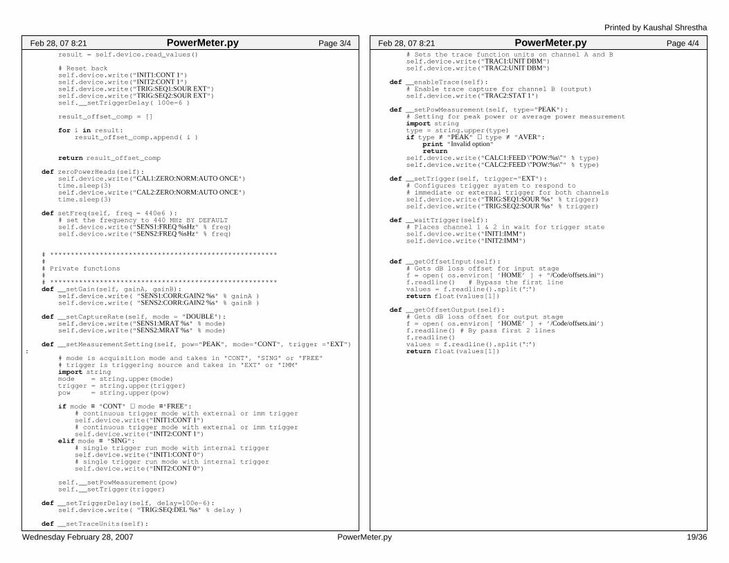
result = self.device.read_values()
# Reset back self.device.write(" INIT1:CONT 1") self.device.write(" INIT2:CONT 1") self.device.write(" TRIG:SEQ1:SOUR EXT") self.device.write(" TRIG:SEQ2:SOUR EXT") self.__setTriggerDelay( 100e−6 )
result_offset_comp = [] for i in result: result_offset_comp.append( i )
return result_offset_comp
def zeroPowerHeads(self): self.device.write(" CAL1:ZERO:NORM:AUTO ONCE") time.sleep(3) self.device.write(" CAL2:ZERO:NORM:AUTO ONCE") time.sleep(3) def setFreq(self, freq = 440e6 ): # set the frequency to 440 MHz BY DEFAULT self.device.write(" SENS1:FREQ %sHz" % freq) self.device.write(" SENS2:FREQ %sHz" % freq)
# ******************************************************* # # Private functions # # ******************************************************* def __setGain(self, gainA, gainB): self.device.write( " SENS1:CORR:GAIN2 %s" % gainA )
self.device.write( " SENS2:CORR:GAIN2 %s" % gainB )
def __setCaptureRate(self, mode = " DOUBLE"): self.device.write(" SENS1:MRAT %s" % mode) self.device.write(" SENS2:MRAT %s" % mode)
def __setMeasurementSetting(self, pow=" PEAK", mode=" CONT", trigger =" EXT"): # mode is acquisition mode and takes in "CONT", "SING" or "FREE" # trigger is triggering source and takes in "EXT" or "IMM" import string mode = string.upper(mode) trigger = string.upper(trigger) pow = string.upper(pow)
if mode ≡ " CONT" ∨ mode ≡" FREE": # continuous trigger mode with external or imm trigger self.device.write(" INIT1:CONT 1") # continuous trigger mode with external or imm trigger self.device.write(" INIT2:CONT 1") elif mode ≡ " SING": # single trigger run mode with internal trigger self.device.write(" INIT1:CONT 0") # single trigger run mode with internal trigger self.device.write(" INIT2:CONT 0") self.__setPowMeasurement(pow) self.__setTrigger(trigger)
def __setTriggerDelay(self, delay=100e−6): self.device.write( " TRIG:SEQ:DEL %s" % delay ) def __setTraceUnits(self):
Feb 28, 07 8:21 Page 3/4PowerMeter.py # Sets the trace function units on channel A and B self.device.write(" TRAC1:UNIT DBM") self.device.write(" TRAC2:UNIT DBM")
def __enableTrace(self): # Enable trace capture for channel B (output) self.device.write(" TRAC2:STAT 1")
def __setPowMeasurement(self, type=" PEAK"): # Setting for peak power or average power measurement import string type = string.upper(type) if type ≠ " PEAK" ∧ type ≠ " AVER": print " Invalid option" return self.device.write(" CALC1:FEED \"POW:%s\"" % type) self.device.write(" CALC2:FEED \"POW:%s\"" % type)
def __setTrigger(self, trigger=" EXT"): # Configures trigger system to respond to # immediate or external trigger for both channels self.device.write(" TRIG:SEQ1:SOUR %s" % trigger) self.device.write(" TRIG:SEQ2:SOUR %s" % trigger)
def __waitTrigger(self): # Places channel 1 & 2 in wait for trigger state self.device.write(" INIT1:IMM ") self.device.write(" INIT2:IMM ")
def __getOffsetInput(self): # Gets dB loss offset for input stage f = open( os.environ[ ’ HOME’ ] + " /Code/offsets.ini") f.readline() # Bypass the first line values = f.readline().split(" :") return float(values[1]) def __getOffsetOutput(self): # Gets dB loss offset for output stage f = open( os.environ[ ’ HOME’ ] + ’ /Code/offsets.ini’) f.readline() # By pass first 2 lines f.readline() values = f.readline().split(" :") return float(values[1])
Feb 28, 07 8:21 Page 4/4PowerMeter.py
Printed by Kaushal Shrestha
Wednesday February 28, 2007 19/36PowerMeter.py

#! /usr/bin/env python
# Power Supply Class is the direct connection between the main computer and# the Agilent Power Supply.# This is the class that should be used to interface with the power supply# This class implements various functions of the power meter using the SCPI# command set.
import socketimport sysimport datetimeimport time
from TestException import *from Utilities import *
class PowerSupply: """ Controls power supply settings for channel 1 (Functions: SetCurr, SetVolt, GetCurr, GetVolt, On, Off, GetOnOff """
IP_ADDR = " 192.168.0.2" SOCKET_NO = 5025 def __init__(self): # Connect to the power supply via ethernet on mfg. default port 5025 self.socket = socket.socket(socket.AF_INET, socket.SOCK_STREAM) self.socket.connect((self.IP_ADDR, self.SOCKET_NO)) self.setPowerOff()
def __del__(self): try: self.setPowerOff() del self.socket except Exception: raise
def setCurr(self,val): # Sets the current limit designted by val in Amps # val takes in a real number between 0 and 5.1 self.socket.send(’ CURR ’+str(val)+’ ,(@1)\n’)
def getVoltageSetpoint(self): self.socket.send(’ VOLT? (@1)\n’) return float(self.socket.recv(100))
def setVolt(self,val): # Sets the voltage limit designated by val in Volts # val takes in a real number between 0 and 61.2 self.socket.send(’ VOLT ’+str(val)+’ ,(@1)\n’)
def getCurr(self): # Measures the current draw from the supply in Amps self.socket.send(’ *OPC?\n’) # Asks if the reading is stable self.socket.recv(100) # We think blocks until above is yes self.socket.send(’ MEAS:CURR? (@1)\n’)
return float(self.socket.recv(100))
def getVoltageReading(self): # Measures the output voltage in Volts self.socket.send(’ MEAS:VOLT? (@1)\n’)
return float(self.socket.recv(100))
def setPowerOn(self): # Enable output and let the caps charge self.socket.send(’ OUTP ON, (@1)\n’)
Feb 28, 07 8:22 Page 1/2PowerSupply.py
# Wait until the output voltage has reached what it has been set to # Typical value is 32V # Time delay to wait for Power Supply to be ready t1 = datetime.datetime.utcnow() set = self.getVoltageSetpoint() time.sleep( 0.25 ) # S meas = self.getVoltageReading() diff = abs( meas − set ) limit = 0.1 # V had_to_loop = False while diff > limit: msg = " VoltageSetpoint: %4.1f V, Reading: %4.1f V, " + \ " Diff = %4.1f V > %.1f V" % ( set, meas, diff, limit ) time.sleep( 0.25 ) # S sys.stdout.write( " \r %s" % msg ) sys.stdout.flush() t2 = datetime.datetime.utcnow() if (t2 − t1) > datetime.timedelta( seconds = 10 ): print " \nSomething’s wrong with the power supply...." self.setPowerOff() raise TestException(TestException.device_error_PowerSupply) set = self.getVoltageSetpoint() meas = self.getVoltageReading() diff = abs( meas − set ) had_to_loop = True
if had_to_loop: msg = " VoltageSetpoint: %4.1f V, Reading: %4.1f V, " + \ " Diff = %4.1f V > %.1f V" % ( set, meas, diff, limit ) sys.stdout.write( " \r %s\n" % msg ) sys.stdout.flush()
def setPowerOff(self): # Disable output self.socket.send(’ OUTP OFF, (@1)\n’)
def getPowerStatus(self): # Get Power Status self.socket.send(’ OUTP? (@1)\n’)
return float(self.socket.recv(100))
Feb 28, 07 8:22 Page 2/2PowerSupply.py
Printed by Kaushal Shrestha
Wednesday February 28, 2007 20/36PowerSupply.py
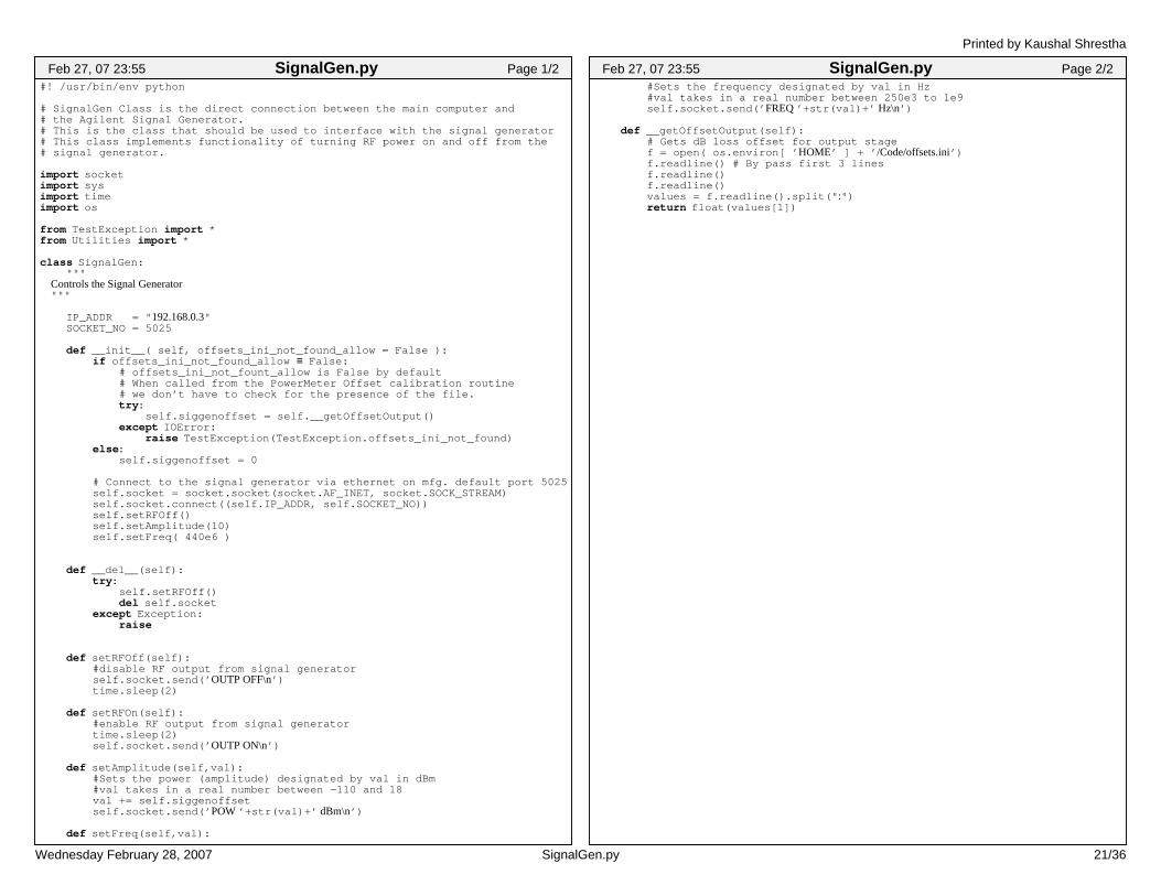
#! /usr/bin/env python
# SignalGen Class is the direct connection between the main computer and# the Agilent Signal Generator.# This is the class that should be used to interface with the signal generator# This class implements functionality of turning RF power on and off from the# signal generator.
import socketimport sysimport timeimport os
from TestException import *from Utilities import *
class SignalGen: """ Controls the Signal Generator """
IP_ADDR = " 192.168.0.3" SOCKET_NO = 5025 def __init__( self, offsets_ini_not_found_allow = False ): if offsets_ini_not_found_allow ≡ False: # offsets_ini_not_fount_allow is False by default # When called from the PowerMeter Offset calibration routine # we don’t have to check for the presence of the file. try: self.siggenoffset = self.__getOffsetOutput() except IOError: raise TestException(TestException.offsets_ini_not_found) else: self.siggenoffset = 0
# Connect to the signal generator via ethernet on mfg. default port 5025 self.socket = socket.socket(socket.AF_INET, socket.SOCK_STREAM) self.socket.connect((self.IP_ADDR, self.SOCKET_NO)) self.setRFOff() self.setAmplitude(10) self.setFreq( 440e6 )
def __del__(self): try: self.setRFOff() del self.socket except Exception: raise
def setRFOff(self): #disable RF output from signal generator self.socket.send(’ OUTP OFF\n’) time.sleep(2)
def setRFOn(self): #enable RF output from signal generator time.sleep(2) self.socket.send(’ OUTP ON\n’)
def setAmplitude(self,val): #Sets the power (amplitude) designated by val in dBm #val takes in a real number between −110 and 18 val += self.siggenoffset self.socket.send(’ POW ’+str(val)+’ dBm\n’)
def setFreq(self,val):
Feb 27, 07 23:55 Page 1/2SignalGen.py #Sets the frequency designated by val in Hz #val takes in a real number between 250e3 to 1e9 self.socket.send(’ FREQ ’+str(val)+’ Hz\n’)
def __getOffsetOutput(self): # Gets dB loss offset for output stage f = open( os.environ[ ’ HOME’ ] + ’ /Code/offsets.ini’) f.readline() # By pass first 3 lines f.readline() f.readline() values = f.readline().split(" :") return float(values[1])
Feb 27, 07 23:55 Page 2/2SignalGen.py
Printed by Kaushal Shrestha
Wednesday February 28, 2007 21/36SignalGen.py
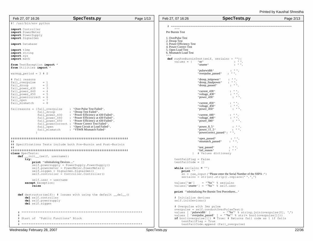
#! /usr/bin/env python
import Controllerimport PowerMeterimport PowerSupplyimport SignalGen
import Database
import timeimport stringimport sysimport math
from TestException import *from Utilities import *
warmup_period = 3 # S
# Fail reasonsfail_overpulse = 1fail_droop = 2fail_power_430 = 3fail_power_440 = 4fail_power_450 = 5fail_powercorrect = 6fail_open = 7fail_mismatch = 8
failreasons = fail_overpulse : " Over Pulse Test Failed", fail_droop : " Droop Test Failed", fail_power_430 : " Power Efficiency at 430 Failed", fail_power_440 : " Power Efficiency at 430 Failed", fail_power_450 : " Power Efficiency at 430 Failed", fail_powercorrect : " Power Correct Test Failed", fail_open : " Open Circuit at Load Failed", fail_mismatch : " VSWR Mismatch Failed"
###################################################################### Specifications Tests include both Pre−Burnin and Post−Burinin####################################################################class SpecTests: def __init__(self, username): try: print " \nInitializing Devices ..." self.powersupply = PowerSupply.PowerSupply() self.powermeter = PowerMeter.PowerMeter() self.siggen = SignalGen.SignalGen() self.controller = Controller.Controller()
self.user = username except Exception: raise
def destructor(self): # Issues with using the default __del__() del self.controller del self.powersupply del self.siggen # ******************************************************************** # # Start of "Public Functions" Block # # ********************************************************************
Feb 27, 07 16:26 Page 1/13SpecTests.py
# ==================================================================== """ Pre Burnin Test
1. OverPulse Test 2. Droop Test 3. Power Efficiency Test 4. Power Correct Test 5. Open Load Test 6. Mismatch Load Test """ def runPreBurninTest(self, serialno = ""): values = " sn" : " ", " uname" : " ", " pulsewidth" : " ", " overpulse_passed" : " ", " droop_initpower" : " ", " droop_finalpower" : " ", " droop_passed" : " ",
" current_430" : " ", " voltage_430" : " ", " power_430" : " ",
" current_450" : " ", " voltage_450" : " ", " power_450" : " ",
" current_440" : " ", " voltage_440" : " ", " power_440" : " ",
" power_8_5" : " ", " power_11_5" : " ", " powercorrect_passed": " ",
" open_passed" : " ", " mismatch_passed" : " ",
" test_passed" : " ", " fail_reason" : " " # Values dictionary
testFailFlag = False testFailCode = [] while serialno ≡ "": print "" sn = raw_input(" Please enter the Serial Number of the SSPA :") serialno = str(sn).strip().replace(" "," _")
values[’ sn’] = " ’%s’" % serialno values[’ uname’] = " ’%s’" % self.user
print " \nInitializing Pre Burnin Test Porcedures..."
# Initialize devices self.initDevices()
# Overpulse with 3ms pulse overpulse = self.conductOverPulseTest() values [ ’ pulsewidth’ ] = " ’%s’" % string.join(overpulse[0], " ,") values [ ’ overpulse_passed’ ] = " ’%s’" % str( ¬ bool(overpulse[1])) if bool(overpulse[1]) ≡ True: # Returns fail code as 1 if fails testFailFlag = True testFailCode.append (fail_overpulse)
Feb 27, 07 16:26 Page 2/13SpecTests.py
Printed by Kaushal Shrestha
Wednesday February 28, 2007 22/36SpecTests.py

# Droop (initpower, finalpower, passed) = self.conductDroopTest() values [ ’ droop_initpower’ ] = " ’%s’" % initpower values [ ’ droop_finalpower’ ] = " ’%s’" % finalpower values [ ’ droop_passed’ ] = " ’%s’" % passed if droop_passed ≡ False: testFailFlag = True testFailCodea.append(fail_droop)
# Efficiency at 430, 440, 450 (currents, voltages, powers, failflag) = self.conductEfficiencyTest() for i in [430,440,450]: # indexex 0,1,2 (430, 440, 450) values [ " current_%s" % i ] = " ’%s’" % currents [i/10 − 43] values [ " voltage_%s" % i ] = " ’%s’" % voltages [i/10 − 43] values [ " power_%s" % i ] = " ’%s’" % powers [i/10 − 43]
testFailFlag = bool(failflag) # returns the fail code and 0 if passed sys.stdout.write ( " Efficiency Test before burnin ...\t" ) if ( testFailFlag ≡ False ): # PASSED setStyle(’ bold’, ’ green’ ) sys.stdout.write(" [ PASSED ]") setStyle(’ default’) else: # Failed setStyle(’ bold’, ’ red’ ) sys.stdout.write(" [ FAILED ]") setStyle(’ default’) testFailCode.append(failflag) # Power Correct powercorrect = self.conductPowerCorrectTest() values [ ’ power_8_5’ ] = powercorrect[0][0] values [ ’ power_11_5’ ] = powercorrect[0][1] values [ ’ powercorrect_passed’ ] = " ’%s’" % \ str( ¬ bool(powercorrect[1])) if bool(powercorrect[1]) ≡ True: testFailFlag = True testFailCode.append(fail_powercorrect) # Open and Mismatch variousloads_passed = self.conductVariousLoadsTest() values [ ’ open_passed’ ] = " ’%s’" % \ str(bool(variousloads_passed[0])) values [ ’ mismatch_passed’ ] = " ’%s’" % \ str(bool(variousloads_passed[1])) if bool(variousloads_passed[0]) ≡ False: testFailFlag = True testFailCode.append(fail_open) if bool(variousloads_passed[1]) ≡ False: testFailFlag = True testFailCode.append(fail_mismatch)
values [ ’ test_passed’ ] = " ’%s’" % str( ¬(testFailFlag)) vals_fails = [] for i in testFailCode: vals_fails.append(" ’%s’" % failreasons[i]) values [ ’ fail_reason’ ] = string.join (vals_fails , ’ ,’) # Save Data # −−−−−−−−−−−−−−−−−−−−−−−−−−−−−−−−−−−−−−−−− self.__savePreBurninResults(values) # −−−−−−−−−−−−−−−−−−−−−−−−−−−−−−−−−−−−−−−−− # End of PreBurinin Procedure print " \n" if testFailFlag ≡ True:
Feb 27, 07 16:26 Page 3/13SpecTests.py setStyle(’ bold’, ’ red’) print 35 * ’ −’ print " PreBurnin Test Failed !!!" print 35 * ’ −’ else: setStyle(’ bold’, ’ green’) print 35 * ’ −’ print " PreBurnin Test Completed !!!" print 35 * ’ −’
setStyle(’ default’)
# ===================================================================
# =================================================================== """ Post Burnin Test
1. OverPulse Test 2. Droop Test 3. Power Efficiency Test 4. Power Correct Test 5. Open Load Test 6. Mismatch Load Test """ def runPostBurninTest(self, serialno = "" ): values = " sn" : " ", " uname" : " ", " pulsewidth" : " ", " overpulse_passed" : " ", " droop_initpower" : " ", " droop_finalpower" : " ", " droop_passed" : " ",
" current_430" : " ", " voltage_430" : " ", " power_430" : " ",
" current_450" : " ", " voltage_450" : " ", " power_450" : " ",
" current_440" : " ", " voltage_440" : " ", " power_440" : " ",
" power_8_5" : " ", " power_11_5" : " ", " powercorrect_passed": " ",
" open_passed" : " ", " mismatch_passed" : " ",
" test_passed" : " ", " fail_reason" : " " # Values dictionary testFailFlag = False testFailCode = [] while serialno ≡ "": print "" sn = raw_input(" Please enter the Serial Number of the SSPA :") serialno = sn.strip().replace(" "," _") values[’ sn’] = " ’%s’" % serialno
Feb 27, 07 16:26 Page 4/13SpecTests.py
Printed by Kaushal Shrestha
Wednesday February 28, 2007 23/36SpecTests.py
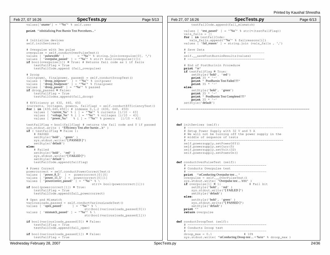
values[’ uname’] = " ’%s’" % self.user print " \nInitializing Post Burnin Test Porcedures..."
# Initialize devices self.initDevices()
# Overpulse with 3ms pulse overpulse = self.conductOverPulseTest() values [ ’ pulsewidth’ ] = " ’%s’" % string.join(overpulse[0], " ,") values [ ’ overpulse_passed’ ] = " ’%s’" % str( ¬ bool(overpulse[1])) if bool(overpulse[1]) ≡ True: # Returns fail code as 1 if fails testFailFlag = True testFailCode.append (fail_overpulse) # Droop (initpower, finalpower, passed) = self.conductDroopTest() values [ ’ droop_initpower’ ] = " ’%s’" % initpower values [ ’ droop_finalpower’ ] = " ’%s’" % finalpower values [ ’ droop_passed’ ] = " ’%s’" % passed if droop_passed ≡ False: testFailFlag = True testFailCodea.append(fail_droop)
# Efficiency at 430, 440, 450 (currents, voltages, powers, failflag) = self.conductEfficiencyTest() for i in [430,440,450]: # indexex 0,1,2 (430, 440, 450) values [ " current_%s" % i ] = " ’%s’" % currents [i/10 − 43] values [ " voltage_%s" % i ] = " ’%s’" % voltages [i/10 − 43] values [ " power_%s" % i ] = " ’%s’" % powers [i/10 − 43]
testFailFlag = bool(failflag) # returns the fail code and 0 if passed sys.stdout.write ( " Efficiency Test after burnin ...\t" ) if ( testFailFlag ≡ False ): # PASSED setStyle(’ bold’, ’ green’ ) sys.stdout.write(" [ PASSED ]") setStyle(’ default’) else: # Failed setStyle(’ bold’, ’ red’ ) sys.stdout.write(" [ FAILED ]") setStyle(’ default’) testFailCode.append(failflag) # Power Correct powercorrect = self.conductPowerCorrectTest() values [ ’ power_8_5’ ] = powercorrect[0][0] values [ ’ power_11_5’ ] = powercorrect[0][1] values [ ’ powercorrect_passed’ ] = " ’%s’" % \ str( ¬ bool(powercorrect[1])) if bool(powercorrect[1]) ≡ True: testFailFlag = True testFailCode.append(fail_powercorrect) # Open and Mismatch variousloads_passed = self.conductVariousLoadsTest() values [ ’ open_passed’ ] = " ’%s’" % \ str(bool(variousloads_passed[0])) values [ ’ mismatch_passed’ ] = " ’%s’" % \ str(bool(variousloads_passed[1])) if bool(variousloads_passed[0]) ≡ False: testFailFlag = True testFailCode.append(fail_open) if bool(variousloads_passed[1]) ≡ False: testFailFlag = True
Feb 27, 07 16:26 Page 5/13SpecTests.py testFailCode.append(fail_mismatch)
values [ ’ test_passed’ ] = " ’%s’" % str( ¬(testFailFlag)) vals_fails = [] for i in testFailCode: vals_fails.append(" ’%s’" % failreasons[i]) values [ ’ fail_reason’ ] = string.join (vals_fails , ’ ,’) # Save Data # −−−−−−−−−−−−−−−−−−−−−−−−−−−−−−−−−−−−−−−−− self.__savePostBurninResults(values) # −−−−−−−−−−−−−−−−−−−−−−−−−−−−−−−−−−−−−−−−− # End of PostBurinin Procedure print " \n" if testFailFlag ≡ True: setStyle(’ bold’, ’ red’) print 35 * ’ −’ print " PostBurnin Test Failed !!!" print 35 * ’ −’ else: setStyle(’ bold’, ’ green’) print 35 * ’ −’ print " PostBurnin Test Completed !!!" print 35 * ’ −’
setStyle(’ default’)
# =====================================================================
def initDevices (self): # −−−−−−−−−−−−−−−−−−−−−−−−−−−−−−−−−−−−−−−−−−−−−−−−−−− # Setup Power Supply with 32 V and 5 A # We will not be turning off the power supply in the # middle of sequence of tests # −−−−−−−−−−−−−−−−−−−−−−−−−−−−−−−−−−−−−−−−−−−−−−−−−−− self.powersupply.setPowerOff() self.powersupply.setCurr(5) self.powersupply.setVolt(32) self.powersupply.setPowerOn()
def conductOverPulseTest (self): # −−−−−−−−−−−−−−−−−−−−−−−−−−−−−−−−−−−−−−−−−− # Conducts Overpulse test # −−−−−−−−−−−−−−−−−−−−−−−−−−−−−−−−−−−−−−−−−− print " \nConducting Overpulse test ... " overpulse = self.__OverPulseTest() sys.stdout.write( " Overpulse test ... \t\t\t" ) if overpulse[1] ≡ 1: # Fail bit setStyle(’ bold’, ’ red’ ) sys.stdout.write(" [ FAILED ]") setStyle(’ default’) else: setStyle(’ bold’, ’ green’ ) sys.stdout.write(" [ PASSED ]") setStyle(’ default’) print "" return overpulse
def conductDroopTest (self): # −−−−−−−−−−−−−−−−−−−−−−−−−−−−−−−−−−−−−−−−−− # Conducts Droop test # −−−−−−−−−−−−−−−−−−−−−−−−−−−−−−−−−−−−−−−−−− droop_max = 0.1 # 10% sys.stdout.write( " \nConducting Droop test ... < %s\n" % droop_max )
Feb 27, 07 16:26 Page 6/13SpecTests.py
Printed by Kaushal Shrestha
Wednesday February 28, 2007 24/36SpecTests.py

initpower, finalpower = self.__DroopTest() # dBm
power_init_mW = 10 ** initpower/ 10.0 power_final_mW = 10 ** finalpower / 10.0 sys.stdout.write( " Droop test ... \t\t\t\t" ) if power_final_mW > ((1 − droop_max) * power_init_mW) : droop_passed = ’ t’ setStyle(’ bold’, ’ green’ ) sys.stdout.write(" [ PASSED ]") setStyle(’ default’) else: droop_passed = ’ f’ setStyle(’ bold’, ’ red’ ) sys.stdout.write(" [ FAILED ]") setStyle(’ default’) print " \n Power at the beginning of pulse is %s mW (%s dBm)" % \ (power_init_mW, initpower) print " Power at the end of pulse is %s mW (%s dBm)" % \ (power_final_mW, finalpower) print "" return (initpower, finalpower, droop_passed)
def conductEfficiencyTest (self): # −−−−−−−−−−−−−−−−−−−−−−−−−−−−−−−−−−−−−−−−−− # Conducts Efficiency test at # 430, 450 and 440 MHz # −−−−−−−−−−−−−−−−−−−−−−−−−−−−−−−−−−−−−−−−−− currents = [] voltages = [] powers = [] print " \nConducting Efficiency test ... " # 430 MHz current, voltage, power = self.__EfficiencyTest( 430e6 ) print " At 430 MHz" print " \tCurrent : %.3f A, Voltage : %.3f V, Power : %.3f dBm"\ % (current, voltage, power)
print " \tEfficiency : %.1f %%" % \((10**(power/10))/10000/(current * voltage)*100)
currents.append(current) voltages.append(voltage) powers.append(power)
# 440 MHz current, voltage, power = self.__EfficiencyTest( 440e6 ) print " At 440 MHz" print " \tCurrent : %.3f A, Voltage : %.3f V, Power : %.3f dBm"\ % (current, voltage, power)
print " \tEfficiency : %.1f %%" % \((10**(power/10))/10000/(current * voltage)*100)
currents.append(current) voltages.append(voltage) powers.append(power)
# 450 MHz current, voltage, power = self.__EfficiencyTest( 450e6 ) print " At 450 MHz" print " \tCurrent : %.3f A, Voltage : %.3f V, Power : %.3f dBm"\ % (current, voltage, power)
print " \tEfficiency : %.1f %%" % \((10**(power/10))/10000/(current * voltage)*100)
currents.append(current) voltages.append(voltage)
Feb 27, 07 16:26 Page 7/13SpecTests.py powers.append(power)
efficiency = 38 # % percentage # the divide 10 is to convert peak power to average power # Note the power is converted into Watts eff_0 = (10**(powers[0]/10)) / 10000 / (currents[0] * voltages[0])* 100 eff_1 = (10**(powers[1]/10)) / 10000 / (currents[1] * voltages[1])* 100 eff_2 = (10**(powers[2]/10)) / 10000 / (currents[2] * voltages[2])* 100 if (eff_0 ≥ efficiency ∧ eff_1 ≥ efficiency ∧ eff_2 ≥ efficiency): # PASSED failflag = 0 else: # Failed if (eff_0 < efficiency): failflag = fail_power_430 elif (eff_1 < efficiency): failflag = fail_power_440 elif (eff_2 < efficiency): failflag = fail_power_450 return (currents, voltages, powers, failflag)
def conductPowerCorrectTest (self): # −−−−−−−−−−−−−−−−−−−−−−−−−−−−−−−−−−−−−−−−−− # Powercorrect test # −−−−−−−−−−−−−−−−−−−−−−−−−−−−−−−−−−−−−−−−−− print ( " \nConducting PowerCorrect test ... " ) powercorrect = self.__PowerCorrectTest() sys.stdout.write( " Powercorrect test... \t\t\t" ) if powercorrect[1] ≡ 1: #Fail bit setStyle(’ bold’, ’ red’ ) sys.stdout.write(" [ FAILED ]\n") setStyle(’ default’) else: setStyle(’ bold’, ’ green’ ) sys.stdout.write(" [ PASSED ]\n") setStyle(’ default’)
return powercorrect
def conductVariousLoadsTest (self): # −−−−−−−−−−−−−−−−−−−−−−−−−−−−−−−−−−−−−−−−−− # Open and 3:1 Mismatch test # −−−−−−−−−−−−−−−−−−−−−−−−−−−−−−−−−−−−−−−−−− print " \nConducting Open and 3:1 VSWR Mismatch test ... "
# Gets a list [open, vswr] passed status variousloads_passed = self.__VariousLoadsTest() return variousloads_passed
# ******************************************************************** # # Start of Private Functions Block # # ********************************************************************
def __OverPulseTest(self): """ Check for the output pulse−limiting behavior of the SSPA """ # −−−−−−−−−−−−−−−−−−−−−−−−−−−−−−−−−−−−−−−−−− # This test supplies 3ms pulses at 25Hz to # the SSPA to test the excessive pulse
Feb 27, 07 16:26 Page 8/13SpecTests.py
Printed by Kaushal Shrestha
Wednesday February 28, 2007 25/36SpecTests.py
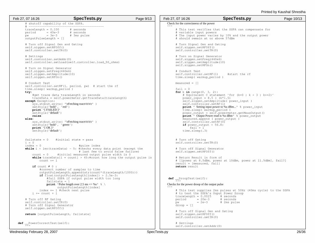
# shutoff capability of the SSPA. # −−−−−−−−−−−−−−−−−−−−−−−−−−−−−−−−−−−−−−−−−− traceLength = 0.100 # seconds period = 40e−3 # seconds pw = 3e−3 # 3ms pulse outputPulseLength = []
# Turn off Signal Gen and Gating self.siggen.setRFOff() self.controller.setTR(0)
# Settings self.controller.setAddr(0) self.controller.setLoad(self.controller.load_50_ohms) # Turn on Signal Generator self.siggen.setFreq(440e6) self.siggen.setAmplitude(10) self.siggen.setRFOn()
# Conduct Test self.controller.setRF(1, period, pw) # start the rf time.sleep( warmup_period ) try: #get trace data traceLength in seconds traceData = self.powermeter.getTraceData(traceLength) except Exception: sys.stdout.write( " \rFetching trace\t\t\t\t" ) setStyle(’ bold’, ’ red’) print " [ FAILED ]" setStyle(’ default’) raise else: sys.stdout.write( " \rFetching trace\t\t\t\t" ) setStyle(’ bold’, ’ green’) print " [ OK ]" setStyle(’ default’)
failstate = 0 #initial state = pass i = 0 index = 0 #pulse index while i < len(traceData) − 5: #checks every data point (except the # last few to avoid false failure) count = 0 #initial measured output pulse width is 0 while traceData[i + count] > 45: #count how long the output pulse is count += 1
if count ≠ 0 : #convert number of samples to time outputPulseLength.append(str(count*(traceLength/1000))) if float(outputPulseLength[index]) > 2.5e−3: #fail SSPA if output pulse width too long failstate = 1 print " Pulse length over 2.5 ms => %s" % \ outputPulseLength[index] index += 1 #check next pulse i += count + 1 # Turn off RF Gating self.controller.setTR(0) # Turn off Signal Generator self.siggen.setRFOff() return [outputPulseLength, failstate]
def __PowerCorrectTest(self): """
Feb 27, 07 16:26 Page 9/13SpecTests.py Check for the correctneess of the power """ # This test verifies that the SSPA can compensate for # variable input powers # The input power varies by 10% and the output power # should remain at or above 57dBm
# Turn Signal Gen and Gating self.siggen.setRFOff() self.controller.setTR(0) # Turn on Signal Generator self.siggen.setFreq(440e6) self.siggen.setAmplitude(10) self.siggen.setRFOn()
# Conduct Test self.controller.setRF(1) #start the rf time.sleep( warmup_period )
measured = [] fail = 0 for k in range(0, 3, 2): # Equivalent C statement ’for (k=0 ; k < 3 ; k+=2)’ power_input = 8.5 + (k*1.5) self.siggen.setAmplitude( power_input ) self.controller.setRF(1) print " Setting input power to %s dBm..." % power_input time.sleep( warmup_period ) power_output = self.powermeter.getMeasOutput() print " Output Power read is %s dBm" % power_output measured.append ( power_output ) self.controller.setRF(0) if power_output < 56.8: fail = 1 time.sleep(.3)
# Turn off Gating self.controller.setTR(0)
# Turn off Signal Generator self.siggen.setRFOff() # Return Result in form of # [[power at 8.5dBm, power at 10dBm, power at 11.5dBm], fail?] result = [measured, fail] return result
def __DroopTest(self): """ Checks for the power droop of the output pulse """ # This test supplies 2ms pulses at 50Hz (40ms cycle) to the SSPA # to test the SSPA’s Ouput Power Droop traceLength = 0.0025 # seconds period = 20e−3 # seconds pw = 2e−3 # 2ms pulse droop = []
# Turn off Signal Gen and Gating self.siggen.setRFOff() self.controller.setTR(0)
# Settings self.controller.setAddr(0)
Feb 27, 07 16:26 Page 10/13SpecTests.py
Printed by Kaushal Shrestha
Wednesday February 28, 2007 26/36SpecTests.py

self.controller.setLoad(self.controller.load_50_ohms) # Turn on Signal Generator self.siggen.setFreq(440e6) self.siggen.setAmplitude(10) self.siggen.setRFOn()
# Conduct Test self.controller.setRF(1, period, pw) # start the rf time.sleep( warmup_period ) # Get trace data for 2.5 ms traceData = self.powermeter.getTraceData(traceLength, 100e−6)
# Turn off RF Gating self.controller.setTR(0) # Turn off Signal Generator self.siggen.setRFOff()
# Now we need to filter out only the pulse as we will be grabbing # values outside the pulse as well filteredData = [] for i in traceData: if i > 50: filteredData.append ( i )
value_max = max( filteredData ) value_min = min( filteredData ) return [ value_max, value_min ]
def __EfficiencyTest(self, freq): # This test supplies RF signal at the given freq to the SSPA # to test the SSPA’s Ouput Power efficiency
# Turn off Signal Gen and Gating self.siggen.setRFOff() self.controller.setTR(0) self.powermeter.setFreq( freq) # Settings self.controller.setAddr(0) self.controller.setLoad(self.controller.load_50_ohms)
# Turn on Signal Generator self.siggen.setFreq( freq ) # Changes the freq self.siggen.setAmplitude(10) self.siggen.setRFOn()
# Turn on RF Gating signal self.controller.setRF(1)
time.sleep( warmup_period ) current = self.powersupply.getCurr() voltage = self.powersupply.getVoltageReading() power = self.powermeter.getMeasOutput()
# Turn off RF Gating self.controller.setTR(0) # Turn off Signal Generator self.siggen.setRFOff()
# Reset powermeter to read 440 MHz
Feb 27, 07 16:26 Page 11/13SpecTests.py self.powermeter.setFreq( 440e6 ) return [current, voltage, power]
def __VariousLoadsTest(self): """ This test supplies RF signal the SSPA with the ouput hooked to various loads and checks if the amplifier shuts off
Returns a python list with the <test>_passed status for each of open and mismatch """ # Turn off and Signal Gen and Gating self.siggen.setRFOff() self.controller.setTR(0)
# Settings self.controller.setAddr(0) # Turn on Signal Generator self.siggen.setAmplitude(10) self.siggen.setRFOn()
# Load :: Open # −−−−−−−−−−−−−−−−−−−−−−−−−−−−−−−−−−−−−−−−−−−−−−−−− # Cold switching done in the setLoad() method print " Performing test with ..."
sys.stdout.write( " OPEN circuit at the load ...\t\t" ) sys.stdout.flush() self.controller.setLoad( self.controller.load_open ) self.controller.setRF( 1 ) time.sleep( warmup_period ) current = self.powersupply.getCurr() # If the amplifier shuts off it should be drawing less than an amp # Cannot use power measurement as power meter crashes if current > 1: # If current is greater than 1 A, try to get the power. open_passed = False setStyle( ’ bold’ , ’ red’ ) print " [ Failed ]" setStyle( ’ default’) power = self.powermeter.getMeasOutput() print " Power found to be %s dBm" % power
else: open_passed = True setStyle( ’ bold’ , ’ green’ ) print " [ PASSED ]" setStyle( ’ default’)
# Load :: VSWR Mismatch 3:1 # −−−−−−−−−−−−−−−−−−−−−−−−−−−−−−−−−−−−−−−−−−−−−−−−− # Cold switching done in the setLoad() method sys.stdout.write( " 3:1 mismatch at the load ...\t\t" ) sys.stdout.flush() # Need to change it to 3:1 mismatch once we get the cable self.controller.setLoad( self.controller.load_3_1_mismatch ) self.controller.setRF( 1 ) time.sleep( warmup_period )
vswr_flag = self.controller.getVSWR_Flag()
if vswr_flag ≡ 1:
Feb 27, 07 16:26 Page 12/13SpecTests.py
Printed by Kaushal Shrestha
Wednesday February 28, 2007 27/36SpecTests.py

vswr_passed = False setStyle( ’ bold’ , ’ red’ ) print " [ Failed ]" setStyle( ’ default’) else: vswr_passed = True setStyle( ’ bold’ , ’ green’ ) print " [ PASSED ]" setStyle( ’ default’)
# Turn off RF Gating self.controller.setTR(0) # Turn off Signal Generator self.siggen.setRFOff() return [ open_passed, vswr_passed]
############################################################ ## Data Saving Routines ############################################################ def __savePreBurninResults(self, results): """ Formats the Pre Burnin data for the database adapter """ names = [ ] values = [ ] for fieldname, value in results.items(): names.append( " %s" % fieldname ) values.append( " %s" % value ) names_str = string.join(names, ’ , ’) values_str = string.join(values, ’ , ’) db = Database.Database() db.storePreBurninReadings(names_str, values_str)
def __savePostBurninResults(self, results): """ Formats the Post Burnin data for the database adapter """ names = [ ] values = [ ] for fieldname, value in results.items(): names.append( " %s" % fieldname ) values.append( " %s" % value ) names_str = string.join(names, ’ , ’) values_str = string.join(values, ’ , ’) db = Database.Database() db.storePostBurninReadings(names_str, values_str)
# ******************************************************************** # End of Private Functions Block # ********************************************************************
Feb 27, 07 16:26 Page 13/13SpecTests.py
Printed by Kaushal Shrestha
Wednesday February 28, 2007 28/36SpecTests.py
#!/usr/bin/env python
import Calibrationimport SpecTestsimport OvenTestimport OffsetCalibration
import stringimport osimport sysimport time
from TestException import *from Utilities import *
class SSPA_Test: def __init__(self): os.system(’ reset’) self.WelcomeScreen()
def WelcomeScreen(self): os.system(’ clear’) setStyle(’ bold’, ’ default’) print 60 * " =" print 5*" " , " Welcome to the AMISR SSPA Automated Test Suite" print 60 * " =" setStyle(’ default’)
def Login(self): print "" print " Please login below (avoid spaces) ... " LoginName = "" while LoginName ≡ "": try: LoginName = str(raw_input(" Username : ")) LoginName = LoginName.strip().replace(" "," _") except KeyboardInterrupt: print " \n" setStyle(’ default’) sys.exit(1) self.UserName = LoginName
def run (self): while True: self.Login() self.WelcomeScreen() while ¬ (self.UserName ≡ ""): print "" print " 0. Log Off", self.UserName print " 1. Calibration" print " 2. Pre Burn−in Test" print " 3. Post Burn−in Test" print " 4. Power Meter Offset Calibration" print " Q. Quit\n"
inp = "" while inp ≡ "": try: inp = raw_input(" \rEnter our choice : ") inp = string.lower( str(inp) ) inp = inp.strip() except KeyboardInterrupt: setStyle( ’ bold’, ’ red’ ) print " \n\nForced Termination By the User ... \n" setStyle( ’ default’ ) return
Feb 28, 07 8:24 Page 1/2SSPA_Test.py if (inp ≡ " q"): return elif (inp ≡ " 0"): self.UserName = "" break proc = None try: # Try ... Finally block try: # Try ... Except block if (inp ≡ " 1"): serialno = −1 proc = Calibration.Calibration(self.UserName) serialno = proc.runCalibration() if serialno ≠ −1 ∨ serialno is ( ¬ None): # calibration successful if serialno <> −1 # returned value is the the SSPA SN print " \n" finaltest = "" while (finaltest ≠ " n" ∧ finaltest ≠ " y"): ans=raw_input(" Do you want to proceed " + \ " with the pre−burnin test?"+\ " [y/n]:") finaltest = str(ans).strip() finaltest = string.lower(finaltest) if finaltest ≡ " y": proc = SpecTests.SpecTests\ ( self.UserName ) proc.runPreBurninTest(serialno) elif (inp ≡ " 2"): proc = SpecTests.SpecTests(self.UserName) proc.runPreBurninTest() elif ( inp ≡ " 3" ): proc = SpecTests.SpecTests(self.UserName) proc.runPostBurninTest() elif (inp ≡ " 4"): proc = OffsetCalibration.OffsetCalibration() proc.CalibrateOffset() except KeyboardInterrupt: setStyle( ’ bold’, ’ red’ ) print " \n\nProcess Terminated By User ... \n" setStyle( ’ default’ ) except TestException, err: setStyle(’ bold’, ’ red’) print " \n", 65 * " −" msg = err.__str__().split(" \n") for _msg in msg: print ’ ’ + _msg print 65 * " −" setStyle( ’ default’ ) print " \n" finally: # Delete the object so that it calls its destructor # to restore settings to default try: proc.destructor() del proc except: pass if __name__ ≡ " __main__": SSPA_Test().run() print " \nPlease wait while the system shuts down... \n\n"
Feb 28, 07 8:24 Page 2/2SSPA_Test.py
Printed by Kaushal Shrestha
Wednesday February 28, 2007 29/36SSPA_Test.py
#!/usr/bin/env python
import sysimport reimport timeimport stringimport urllib2import datetimeimport pytz
from Utilities import *from TestException import *
class TempSensor: """ TempSensor does a HTTP GET on a URL to capture a string of temperatures from a probe located at Toolik Alaska, and then stores the results in a database through the supporting Database class """
sensor = " 192.168.0.4"
def __init__( self ): """ """
def getTemperature( self ): sensor_reading = self.__getSensaTronicTemps( self.sensor ) return sensor_reading
def __getSensaTronicTemps( self, sensor ): """ Return a dict[ probe_name ] = probe_value The probe_values are assumed to be in F.
An unconnected sensor port will report −99.9. It is worth reporting these in case a wire comes loose, however if we have a 16 port sensor with only 2 ports in use then it is foolish to report the other 14 ports all the time. So we need someway of determining of a port is actually in use.
We count on the configuration of the sensor for this. The default probe name is ’probeN’. If we find a default name then we assume that the port is not in use and don’t bother with it’s −99.9 reading. As a check to this we will logg a warning to any actual value found on the port with a default name. """ probe_re = re.compile( " Probe \d1,2" ) # SensaTronic’s embedded HTTP server offers the page "temps" # to get the current readings. url = " http://%s/temp" % sensor
try: fid = urllib2.urlopen( url ) except urllib2.HTTPError, e: # Errors such as 404, Not Found msg = " HTTPError: %s" % e print msg return None except urllib2.URLError, e: # Errors in the format of the URL or a timeout msg = " URLError: %s" % e print msg return None
Feb 28, 07 8:26 Page 1/2TempSensor.py data = fid.read() fid.close() # "SwitchRoom|reading0|EngineRoom|reading1|probe2|reading2" fields = data.split( ’ |’ )
# Make sure we have an even number of fields, name|reading pairs n_fields = len( fields ) if n_fields % 2 ≠ 0: msg = " Odd number of fields in \"%s\"" % data
print msg return None
# Our dict to return sensor_readings =
# Separate the probes n_probes = n_fields / 2 for i in range( n_probes ): probe_name = fields[ i * 2 ] probe_reading_str = fields[ i * 2 + 1 ]
if probe_re.match( probe_name ): # Default probe name so we assume not in use # But should also have no legitimate value. if probe_reading_str ≠ " −99.9": probe_reading = float( probe_reading_str ) # deg F probe_reading = (probe_reading − 32) * 5 / 9.0 # deg C return probe_reading
msg = " Actual reading (%s) on un−named probe %s" % \ ( probe_reading_str, probe_name ) print msg else: sensor_readings[ probe_name ] = probe_reading
return −99.9
if __name__ ≡ " __main__": print TempSensor().getTemperature()
Feb 28, 07 8:26 Page 2/2TempSensor.py
Printed by Kaushal Shrestha
Wednesday February 28, 2007 30/36TempSensor.py

"""Class that handles the TestResults (The Calibration process and the actual test) along with the Handling of various exceptions."""
class TestException (Exception): device_error_PowerSupply = 100 # Cannot handshake with the Power Supply device_error_PowerMeter = 101 # Cannot handshake with the Power Meter device_error_DAQCard = 102 # Cannot handshake with the DAQ device_error_SignalGen = 103 # Cannot handshake with the Signal Generator device_error_SSPA_Power = 104 # Cannot handshake with the SSPA calib_initialCurrFailed = 200 # Initial current above 0.5 A during Cal calib_gatePulseFailed = 201 # Current is above 0.5A with only gate pulse calib_normalCurrFailed = 202 # Current is out of range calib_driverCurrFailed = 203 # Current out of bounds Pot 1 (Driver Bias) calib_outputCurrFailed = 204 # Current out of bounds Pot 2 (Output Bias) calib_outputPowerFailed = 205 # Power out of bounds Pot 3 (Power Level) calib_phaseFailed = 206 # Phase out of bounds Pot 4 (Phase) calib_vswrFailed = 207 # VSWR out of bounds Pot 5 (VSWR)
calib_offsetCalibfailed = 208 # Power Meter Offset Calibration failed
offsets_ini_not_found = 300 # Offsets.init not found
process_abort_calib = 500 # Abort Calibration Process process_abort_offsetcalib= 501 # Abort Offset Calibration Process
invalid_data_type = 700 # Invalid data type invalid_offsets = 701 # Invalid offset values in offsets.ini
# Key:Value pair for device errors and corresponding strings eStr =device_error_PowerSupply : \ " Cannot establish connection to the Power Supply.\n" + \ " Please check the connections and the power is turned on.", device_error_PowerMeter : \ " Cannot establish connection to the Power Meter.\n" + \ " Please check the connections and the power turned on.", device_error_SignalGen : \ " Cannot establish connection to the Signal Generator.\n" + \ " Please check the connections and the power turned on.", device_error_DAQCard : \ " Driver issue with DAQ Card." + \ " Please contact the administrator.", device_error_SSPA_Power : \ " Cannot establish connection to the SSPA.\n" + \ " Please check the power connections.", calib_initialCurrFailed : \ " Initial current during calibration is above 0.5A", calib_gatePulseFailed : \ " Current exceeds 0.5A with only gate pulse turned on", calib_normalCurrFailed : \ " Current drawn from the power supply out of bounds", calib_driverCurrFailed : \ " Current out of bounds while setting Address 1 (Driver Bias)", calib_outputCurrFailed : \ " Current out of bounds while setting Address 2 (Output Bias)", calib_outputPowerFailed : \ " Power out of bounds while setting Address 4 (Power Level)", calib_phaseFailed : \ " Phase out of bounds while setting Address 5 (Phase)", calib_vswrFailed : \ " Pots out of bounds while setting Address 6 (VSWR)", calib_offsetCalibfailed : \ " Offset Calibration failed.\nPlease check the connections, & \n" +\ " Run the Offset Calibration test again.",
Feb 28, 07 0:11 Page 1/2TestException.py offsets_ini_not_found : \ " Offsets.ini file not found. \n" + \ " Please run the Power Meter Offset Calibration Procedure.", process_abort_calib : " Aborting Calibration Process ...", process_abort_offsetcalib: " Aborting Offset Calibration Process...", invalid_data_type : " Invalid parameter trapped", invalid_offsets : \ " Invalid values for offsets found in offsets.ini file.\n" + \ " Please Re−Calibrate the Offsets before proceeding." def __init__(self, value): self.errno = value
def __str__(self): try: return str(self.eStr[self.errno]) except: return " Unexpected and unhandled error. %s" % self.errno
Feb 28, 07 0:11 Page 2/2TestException.py
Printed by Kaushal Shrestha
Wednesday February 28, 2007 31/36TestException.py
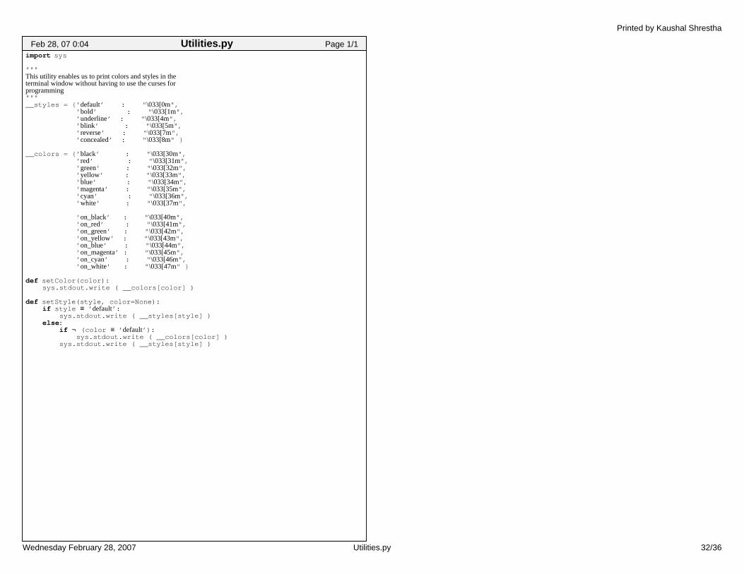
import sys
"""This utility enables us to print colors and styles in theterminal window without having to use the curses forprogramming"""__styles = ’ default’ : " \033[0m", ’ bold’ : " \033[1m", ’ underline’ : " \033[4m", ’ blink’ : " \033[5m", ’ reverse’ : " \033[7m", ’ concealed’ : " \033[8m"
__colors = ’ black’ : " \033[30m", ’ red’ : " \033[31m", ’ green’ : " \033[32m", ’ yellow’ : " \033[33m", ’ blue’ : " \033[34m", ’ magenta’ : " \033[35m", ’ cyan’ : " \033[36m", ’ white’ : " \033[37m",
’ on_black’ : " \033[40m", ’ on_red’ : " \033[41m", ’ on_green’ : " \033[42m", ’ on_yellow’ : " \033[43m", ’ on_blue’ : " \033[44m", ’ on_magenta’ : " \033[45m", ’ on_cyan’ : " \033[46m", ’ on_white’ : " \033[47m"
def setColor(color): sys.stdout.write ( __colors[color] )
def setStyle(style, color=None): if style ≡ ’ default’: sys.stdout.write ( __styles[style] ) else: if ¬ (color ≡ ’ default’): sys.stdout.write ( __colors[color] ) sys.stdout.write ( __styles[style] )
Feb 28, 07 0:04 Page 1/1Utilities.py
Printed by Kaushal Shrestha
Wednesday February 28, 2007 32/36Utilities.py

#include <stdlib.h>#include <stdio.h>#include <NIDAQmx.h>#include <math.h>#include <string.h>
#define DAQmxErrChk(functionCall) if( DAQmxFailed(error=(functionCall)) ) \ goto Error; else
float 64 * acquireData( int samples_per_channel, float pulse_width, int *length);int writetofile( float 64 *data, int size);int loadCounter( int start, int rf, double ipp, double pw);uInt8 * readDigital(uInt8 *data);int writeDigital( int port, char lines[], char values[]);
/* Python Wrapper *//* Written by Kaushal Shrestha *//* January 31, 2007 */// ==================================================================
#include " Python.h"
PyObject *Convert_Big_Array(PyObject *pylist, double array[], int start, int end) int i = 0, j; int length = end − start; pylist = PyList_New( length );
for (i=0, j=start; i < length;j++, i++) PyList_SetItem(pylist, i, PyFloat_FromDouble(array[j])); //printf("%f \n",array[i]); return pylist;
PyObject *py_acquireData(PyObject *self, PyObject *args)
int samples_per_channel = 1000; float pulsewidth = 0.02*3; float 64 *data; int length; PyObject *pylist1, *pylist2, *pylist3;
if ( ¬PyArg_ParseTuple(args," if ", &samples_per_channel, &pulsewidth )) printf(" Restoring to default"); if ( ¬PyArg_ParseTuple(args,"" )) return Py_BuildValue(" d",−1);
//printf("%d %f",samples_per_channel,pulsewidth); data = acquireData(samples_per_channel, pulsewidth, &length); pylist1 = Convert_Big_Array( pylist1, data, 0, length/3 ); pylist2 = Convert_Big_Array( pylist2, data, length / 3, length * 2/3 ); pylist3 = Convert_Big_Array( pylist3, data, length*2/3, length ); return Py_BuildValue( " [OOO]", pylist1, pylist2, pylist3 );
PyObject *py_loadTimers (PyObject *self, PyObject *args) int trrf = 0; // 0 is only TR 1 is both TR and RF float period = 0; float pw = 0; // Duty cycle in percentage if ( ¬PyArg_ParseTuple(args," iff ", &trrf, &period, &pw)) return Py_BuildValue(" i",−1);
Feb 28, 07 0:21 Page 1/7DAQ.c loadCounter(1, trrf, period, pw); return Py_BuildValue(" i",1);
PyObject *py_stopTimers (PyObject *self, PyObject *args) if ( ¬PyArg_ParseTuple(args,"")) return Py_BuildValue(" i",−1); loadCounter(0,0,0,0); return Py_BuildValue(" d",1);
PyObject *py_readDigital (PyObject *self, PyObject *args) uInt8 *value; if ( ¬PyArg_ParseTuple(args,"")) return Py_BuildValue(" i",−1); value = readDigital(value); return Py_BuildValue(" ii ", value[0], value[1]);
PyObject *py_writeDigital (PyObject *self, PyObject *args) int port; char *lines; char *values; if ( ¬PyArg_ParseTuple( args, " iss", /* int, string, string */ &port, &lines, &values)) return Py_BuildValue(" i",−1); return Py_BuildValue( " i", /* return an int */ writeDigital(port, lines, values));
static PyMethodDef DAQ_methods[] = " acquireData", py_acquireData, METH_VARARGS, " loadTimers", py_loadTimers, METH_VARARGS, " stopTimers", py_stopTimers, METH_VARARGS, " readDigital", py_readDigital, METH_VARARGS, " writeDigital", py_writeDigital, METH_VARARGS, NULL, NULL // Sentinel;
void initDAQ() PyObject *m = Py_InitModule(" DAQ",DAQ_methods);
// ==================================================================
float 64 *acquireData( int samples_per_channel, float pulse_width, int *length ) int No_of_Channels = 3; int Post_Trigger_Samples_Per_Channel = 20; /* min is 2 */ int samples = No_of_Channels * samples_per_channel; //total number of samples including int BuffSize=samples + No_of_Channels * Post_Trigger_Samples_Per_Channel; float samplingrate = BuffSize / pulse_width; // Check if the samplingrate exceed 250KSamples/sec, the limit of the DAQ if (samplingrate * No_of_Channels > 250000) samplingrate = 250000 / No_of_Channels; BuffSize = ceil(samplingrate * pulse_width);
Feb 28, 07 0:21 Page 2/7DAQ.c
Printed by Kaushal Shrestha
Wednesday February 28, 2007 33/36ansi_c/DAQ.c
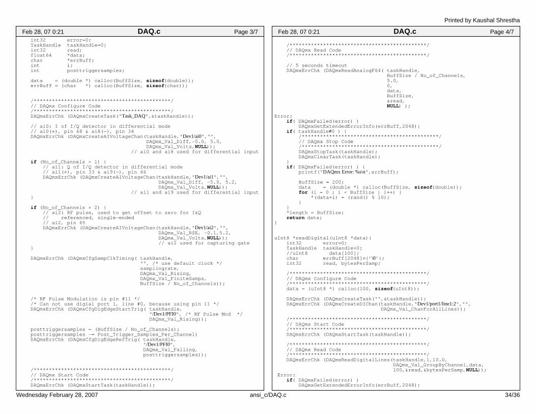
int 32 error=0; TaskHandle taskHandle=0; int 32 read; float 64 *data; char *errBuff; int i; int posttriggersamples;
data = ( double *) calloc(BuffSize, sizeof( double )); errBuff = ( char *) calloc(BuffSize, sizeof( char ));
/*********************************************/ // DAQmx Configure Code /*********************************************/ DAQmxErrChk (DAQmxCreateTask(" Task_DAQ",&taskHandle));
// ai0: I of I/Q detector in differential mode // ai0(+), pin 68 & ai8(−), pin 34 DAQmxErrChk (DAQmxCreateAIVoltageChan(taskHandle," Dev1/ai0","",
DAQmx_Val_Diff,−5.0, 5.0, DAQmx_Val_Volts, NULL));
// ai0 and ai8 used for differential input
if (No_of_Channels > 1) // ai1: Q of I/Q detector in differential mode // ai1(+), pin 33 & ai9(−), pin 66 DAQmxErrChk (DAQmxCreateAIVoltageChan(taskHandle," Dev1/ai1","",
DAQmx_Val_Diff, −5.0, 5.2, DAQmx_Val_Volts, NULL));
// ai1 and ai9 used for differential input
if (No_of_Channels > 2) // ai2: RF pulse, used to get offset to zero for I&Q // referenced, single−ended // ai2, pin 65 DAQmxErrChk (DAQmxCreateAIVoltageChan(taskHandle," Dev1/ai2","",
DAQmx_Val_RSE, −0.1,5.2, DAQmx_Val_Volts, NULL));
// ai2 used for capturing gate
DAQmxErrChk (DAQmxCfgSampClkTiming( taskHandle, "", /* use default clock */ samplingrate, DAQmx_Val_Rising, DAQmx_Val_FiniteSamps, BuffSize / No_of_Channels));
/* RF Pulse Modulation is pin #11 */ /* Can not use digial port 1, line #0, because using pin 11 */ DAQmxErrChk (DAQmxCfgDigEdgeStartTrig( taskHandle, " /Dev1/PFI0", /* RF Pulse Mod */ DAQmx_Val_Rising));
posttriggersamples = (BuffSize / No_of_Channels); posttriggersamples −= Post_Trigger_Samples_Per_Channel) DAQmxErrChk (DAQmxCfgDigEdgeRefTrig( taskHandle, " /Dev1/PFI0", DAQmx_Val_Falling, posttriggersamples));
/*********************************************/ // DAQmx Start Code /*********************************************/ DAQmxErrChk (DAQmxStartTask(taskHandle));
Feb 28, 07 0:21 Page 3/7DAQ.c
/*********************************************/ // DAQmx Read Code /*********************************************/
// 5 seconds timeout DAQmxErrChk (DAQmxReadAnalogF64( taskHandle, BuffSize / No_of_Channels, 5.0, 0, data, BuffSize, &read, NULL) ); Error: if( DAQmxFailed(error) ) DAQmxGetExtendedErrorInfo(errBuff,2048); if( taskHandle ≠0 ) /*********************************************/ // DAQmx Stop Code /*********************************************/ DAQmxStopTask(taskHandle); DAQmxClearTask(taskHandle); if( DAQmxFailed(error) ) printf(" DAQmx Error: %s\n",errBuff);
BuffSize = 200; data = ( double *) calloc(BuffSize, sizeof( double )); for (i = 0 ; i < BuffSize ; i++) *(data+i) = (rand() % 10); *length = BuffSize; return data;
uInt8 *readDigital(uInt8 *data) int 32 error=0; TaskHandle taskHandle=0; //uInt8 data[100]; char errBuff[2048]=’ \0’; int 32 read, bytesPerSamp; /*********************************************/ // DAQmx Configure Code /*********************************************/ data = (uInt8 *) calloc(100, sizeof(uInt8));
DAQmxErrChk (DAQmxCreateTask("",&taskHandle)); DAQmxErrChk (DAQmxCreateDIChan(taskHandle," Dev1/port1/line1:2","",
DAQmx_Val_ChanForAllLines));
/*********************************************/ // DAQmx Start Code /*********************************************/ DAQmxErrChk (DAQmxStartTask(taskHandle)); /*********************************************/ // DAQmx Read Code /*********************************************/ DAQmxErrChk (DAQmxReadDigitalLines(taskHandle,1,10.0,
DAQmx_Val_GroupByChannel,data, 100,&read,&bytesPerSamp, NULL));
Error: if( DAQmxFailed(error) ) DAQmxGetExtendedErrorInfo(errBuff,2048);
Feb 28, 07 0:21 Page 4/7DAQ.c
Printed by Kaushal Shrestha
Wednesday February 28, 2007 34/36ansi_c/DAQ.c

if( taskHandle ≠0 ) /*********************************************/ // DAQmx Stop Code /*********************************************/ DAQmxStopTask(taskHandle); DAQmxClearTask(taskHandle); if( DAQmxFailed(error) ) printf(" DAQmx Error: %s\n",errBuff);
return data;
int writeDigital( int port, char lines[], char values[]) int error=0;
/* See the note below about keeping the port in force when a task handle is cleared. */ TaskHandle taskHandle = 0; char errBuff[2048]=’ \0’; uInt8 *data; int i;
// 012345678901234567 char line[] = " Dev1/portN/line0:7";
line[9] = port + 48; /* convert int to ascii */ line[15]= lines[0]; line[17]= lines[strlen(lines)−1]; data = (uInt8 *) calloc (strlen(values), sizeof(uInt8));
for (i = 0 ; i < strlen(values) ; i++) data[i] = values[i] − 48; /* convert from ascii to int */
/*********************************************/ // DAQmx Configure Code /*********************************************/ DAQmxErrChk (DAQmxCreateTask("",&taskHandle)); DAQmxErrChk (DAQmxCreateDOChan( taskHandle, line, "", /* default clock */ DAQmx_Val_ChanForAllLines ));
/*********************************************/ // DAQmx Start Code /*********************************************/ DAQmxErrChk (DAQmxStartTask(taskHandle)); /*********************************************/ // DAQmx Write Code /*********************************************/ DAQmxErrChk (DAQmxWriteDigitalLines( taskHandle, 1, 1, 10.0, DAQmx_Val_GroupByChannel, data, NULL, NULL)); Error: if( DAQmxFailed(error) ) DAQmxGetExtendedErrorInfo(errBuff,2048); if( taskHandle ≠0 ) /*********************************************/ // DAQmx Stop CodeDAQmxErrChk ( /*********************************************/ /* Digital functions remain in force even when the task is cleared. This is not so for timer tasks. See also loadCounter. */ DAQmxStopTask(taskHandle);
Feb 28, 07 0:21 Page 5/7DAQ.c DAQmxClearTask(taskHandle);
if( DAQmxFailed(error) ) printf(" DAQmx Error: %s\n",errBuff); return 1;
int loadCounter( int start, int rf, double ipp, double pw) double delay = 1.0 / 1000000; // 1us delay double dutycycle1 = pw / ipp; double dutycycle2 = (pw + 2 * delay) / ipp; // duty cycle for TR double freq = 1.0 / ipp; int error=0;
/* Most of the routines use local’s for TaskHandle, but the timers * require static handles that are not destroyed upon function returns */ static TaskHandle taskHandle1=0, taskHandle2 = 0;
char errBuff[2048]=’ \0’; /*********************************************/ // DAQmx Configure Code /*********************************************/ if( taskHandle1 ≠0 ) /*********************************************/ // DAQmx Stop Code /*********************************************/ DAQmxStopTask(taskHandle1); DAQmxClearTask(taskHandle1); taskHandle1 = 0;
if( taskHandle2 ≠0 ) /*********************************************/ // DAQmx Stop Code /*********************************************/ DAQmxStopTask(taskHandle2); DAQmxClearTask(taskHandle2); taskHandle2 = 0;
if ( start ≡ 0 ) return 0;
if (rf ≡ 1) DAQmxErrChk (DAQmxCreateTask(" Counter_1",&taskHandle1));
DAQmxErrChk (DAQmxCreateTask(" Counter_2",&taskHandle2));
// Counter 0 is RF // Counter 1 is TR if (rf ≡ 1) DAQmxErrChk (DAQmxCreateCOPulseChanFreq(taskHandle1," Dev1/ctr0","",
DAQmx_Val_Hz,DAQmx_Val_Low, delay, freq, dutycycle1));
DAQmxErrChk (DAQmxCreateCOPulseChanFreq(taskHandle2," Dev1/ctr1","",
DAQmx_Val_Hz,DAQmx_Val_Low, 0.00, freq, dutycycle2));
// Trigger Counter 0 on rising edge of 1
Feb 28, 07 0:21 Page 6/7DAQ.c
Printed by Kaushal Shrestha
Wednesday February 28, 2007 35/36ansi_c/DAQ.c
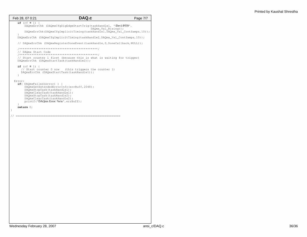
if (rf ≡ 1) DAQmxErrChk (DAQmxCfgDigEdgeStartTrig(taskHandle1, " /Dev1/PFI9",
DAQmx_Val_Rising)); DAQmxErrChk(DAQmxCfgImplicitTiming(taskHandle1,DAQmx_Val_ContSamps,10)); DAQmxErrChk (DAQmxCfgImplicitTiming(taskHandle2,DAQmx_Val_ContSamps,10));
// DAQmxErrChk (DAQmxRegisterDoneEvent(taskHandle,0,DoneCallback,NULL)); /*********************************************/ // DAQmx Start Code /*********************************************/ // Start counter 1 first (because this is what is waiting for trigger) DAQmxErrChk (DAQmxStartTask(taskHandle2));
if (rf ≡ 1) // Start counter 0 now (this triggers the counter 1) DAQmxErrChk (DAQmxStartTask(taskHandle1));
Error: if( DAQmxFailed(error) ) DAQmxGetExtendedErrorInfo(errBuff,2048); DAQmxStopTask(taskHandle1); DAQmxClearTask(taskHandle1); DAQmxStopTask(taskHandle2); DAQmxClearTask(taskHandle2); printf(" DAQmx Error: %s\n",errBuff); return 0;
// ============================================================
Feb 28, 07 0:21 Page 7/7DAQ.c
Printed by Kaushal Shrestha
Wednesday February 28, 2007 36/36ansi_c/DAQ.c

Appendix E
Distribution Board Component Data Sheets
F -1
Table of Contents 1. 2N7002: N-Channel Enhancement Mode Field Effect Transistor.............................F-3 2. 74AC74: Dual D-Type Positive Edge Triggered Flip-Flop.....................................F-11 3. SN74AHCT14: Hex Schmitt-Trigger Inverter ........................................................F-22 4. SN74ALS08: Quadruple 2-Input Positive-AND Gates ...........................................F-38 5. SN74HCT74: Dual D-Type Positive-Edge-Triggered Flip Flops ...........................F-53 6. SN74AHCT541: Octal Buffers/Drivers with 3-State Outputs.................................F-67 7. SN74HC21: Dual 4-Input Positive-AND Gates ......................................................F-82 8. 564-0700-111F: 3mm LED CBI Tri-Level Circuit Board Indicator .......................F-95 9. HEF4521B: 24-Stage Frequency Divider and Oscillator ........................................F-97 10. 179-009-513R571: Center Dual Port D-SUB Female/Female ..............................F-109 11. LTC1441/SO: Ultra Low Power Dual Comparator with Reference......................F-111 12. 5227161-2: BNC Jack, Right Angle ......................................................................F-128 13. PJ-102BH: DC Power Jack....................................................................................F-130
F -2
1. 2N7002: N-Channel Enhancement Mode Field Effect Transistor
Fairchild Semiconductor N-Channel Enhancement Mode
Field Effect Transistor 2N7002
F -3

Electrical Characteristics TA = 25°C unless otherwise noted
Symbol Parameter Conditions Type Min Typ Max Units
OFF CHARACTERISTICS
BVDSS Drain-Source Breakdown Voltage VGS = 0 V, ID = 10 µA All 60 V
IDSS Zero Gate Voltage Drain Current VDS = 48 V, VGS = 0 V 2N7000 1 µA
TJ=125°C 1 mAVDS = 60 V, VGS = 0 V 2N7002
NDS7002A1 µA
TJ=125°C 0.5 mAIGSSF Gate - Body Leakage, Forward VGS = 15 V, VDS = 0 V 2N7000 10 nA
VGS = 20 V, VDS = 0 V 2N7002NDS7002A
100 nA
IGSSR Gate - Body Leakage, Reverse VGS = -15 V, VDS = 0 V 2N7000 -10 nAVGS = -20 V, VDS = 0 V 2N7002
NDS7002A-100 nA
ON CHARACTERISTICS (Note 1)
VGS(th) Gate Threshold Voltage VDS = VGS, ID = 1 mA 2N7000 0.8 2.1 3 V
VDS = VGS, ID = 250 µA 2N7002NDS7002A
1 2.1 2.5
RDS(ON) Static Drain-Source On-Resistance VGS = 10 V, ID = 500 mA 2N7000 1.2 5 ΩTJ =125°C 1.9 9
VGS = 4.5 V, ID = 75 mA 1.8 5.3VGS = 10 V, ID = 500 mA 2N7002 1.2 7.5
TJ =100°C 1.7 13.5VGS = 5.0 V, ID = 50 mA 1.7 7.5
TJ =100C 2.4 13.5VGS = 10 V, ID = 500 mA NDS7002A 1.2 2
TJ =125°C 2 3.5VGS = 5.0 V, ID = 50 mA 1.7 3
TJ =125°C 2.8 5VDS(ON) Drain-Source On-Voltage VGS = 10 V, ID = 500 mA 2N7000 0.6 2.5 V
VGS = 4.5 V, ID = 75 mA 0.14 0.4VGS = 10 V, ID = 500mA 2N7002 0.6 3.75VGS = 5.0 V, ID = 50 mA 0.09 1.5VGS = 10 V, ID = 500mA NDS7002A 0.6 1VGS = 5.0 V, ID = 50 mA 0.09 0.15
2N7000.SAM Rev. A1

Electrical Characteristics TA = 25oC unless otherwise noted
Symbol Parameter Conditions Type Min Typ Max UnitsON CHARACTERISTICS Continued (Note 1)
ID(ON) On-State Drain Current VGS = 4.5 V, VDS = 10 V 2N7000 75 600 mAVGS = 10 V, VDS > 2 VDS(on) 2N7002 500 2700VGS = 10 V, VDS > 2 VDS(on) NDS7002A 500 2700
gFS Forward Transconductance VDS = 10 V, ID = 200 mA 2N7000 100 320 mSVDS > 2 VDS(on), ID = 200 mA 2N7002 80 320VDS > 2 VDS(on), ID = 200 mA NDS7002A 80 320
DYNAMIC CHARACTERISTICSCiss Input Capacitance VDS = 25 V, VGS = 0 V,
f = 1.0 MHzAll 20 50 pF
Coss Output Capacitance All 11 25 pFCrss Reverse Transfer Capacitance All 4 5 pFton Turn-On Time VDD = 15 V, RL = 25 Ω,
ID = 500 mA, VGS = 10 V, RGEN = 25
2N7000 10 ns
VDD = 30 V, RL = 150 Ω,ID = 200 mA, VGS = 10 V,RGEN = 25 Ω
2N700NDS7002A
20
toff Turn-Off Time VDD = 15 V, RL = 25 Ω, ID = 500 mA, VGS = 10 V, RGEN = 25
2N7000 10 ns
VDD = 30 V, RL = 150 Ω,ID = 200 mA, VGS = 10 V,RGEN = 25 Ω
2N700NDS7002A
20
DRAIN-SOURCE DIODE CHARACTERISTICS AND MAXIMUM RATINGSIS Maximum Continuous Drain-Source Diode Forward Current 2N7002 115 mA
NDS7002A 280ISM Maximum Pulsed Drain-Source Diode Forward Current 2N7002 0.8 A
NDS7002A 1.5VSD Drain-Source Diode Forward
VoltageVGS = 0 V, IS = 115 mA (Note 1) 2N7002 0.88 1.5 VVGS = 0 V, IS = 400 mA (Note 1) NDS7002A 0.88 1.2
Note:1. Pulse Test: Pulse Width < 300µs, Duty Cycle < 2.0%.
2N7000.SAM Rev. A1

2N7000.SAM Rev. A1
0 1 2 3 4 50
0.5
1
1.5
2
V , DRAIN-SOURCE VOLTAGE (V)
I ,
DR
AIN
-SO
UR
CE
CU
RR
ENT
(A)
9.0
4.0
8.0
3.0
7.0
V = 10VGS
DS
D
5.0
6.0
-50 -25 0 25 50 75 100 125 1500.5
0.75
1
1.25
1.5
1.75
2
T , JUNCTION TEMPERATURE (°C)
DR
AIN
-SO
UR
CE
ON
-RES
ISTA
NC
E
J
R
, N
OR
MAL
IZED
DS(
ON
)
V = 10VGSI = 500m AD
-50 -25 0 25 50 75 100 125 1500.8
0.85
0.9
0.95
1
1.05
1.1
T , JUNCTION TEM PERATURE (°C)
GAT
E-SO
UR
CE
THR
ESH
OLD
VO
LTAG
E
J
I = 1 m AD
V = VDS GS
V ,
NO
RM
ALIZ
EDth
0 0.4 0.8 1.2 1.6 20.5
1
1.5
2
2.5
3
I , DRA IN CURRENT (A)
DR
AIN
-SO
UR
CE
ON
-RES
ISTA
NC
E
V =4.0V GS
D
R
, N
OR
MAL
IZED
DS(
on)
7.0
4.5
10
5.0
6.0
9.08.0
0 0.4 0.8 1.2 1.6 20
0.5
1
1.5
2
2.5
3
I , DRAIN CURRENT (A)
DR
AIN
-SO
UR
CE
ON
-RES
ISTA
NC
E
T = 125°CJ
25°C
-55°C
D
V = 10V GS
R
, N
OR
MAL
IZED
DS(
on)
Typical Electrical Characteristics
Figure 1. On-Region Characteristics Figure 2. On-Resistance Variation with GateVoltage and Drain Current
Figure 3. On-Resistance Variationwith Temperature
Figure 4. On-Resistance Variation with DrainCurrent and Temperature
Figure 5. Transfer Characteristics Figure 6. Gate Threshold Variation withTemperature
0 2 4 6 8 100
0.4
0.8
1.2
1.6
2
V , GATE TO SOURCE VOLTAGE (V)
I ,
DR
AIN
CU
RR
ENT
(A)
V = 10VDS
GS
D
T = -55°CJ 25°C125°C
2N7000 / 2N7002 / NDS7002A

2N7000.SAM Rev. A1
-50 -25 0 25 50 75 100 125 1500.925
0.95
0.975
1
1.025
1.05
1.075
1.1
T , JUNCTION TEM PERATURE (°C)
DR
AIN
-SO
UR
CE
BREA
KDO
WN
VO
LTAG
E
J
BV
,
NO
RM
ALIZ
EDD
SS
I = 250µAD
0.2 0.4 0.6 0.8 1 1.2 1.40.001
0.005
0.01
0.05
0.1
0.5
1
2
V , BODY DIODE FORWARD VOLTAGE (V)
I ,
REV
ERSE
DR
AIN
CU
RR
ENT
(A)
V = 0VGS
T = 125°CJ
SD
S
25°C
-55°C
0 0.4 0.8 1.2 1.6 20
2
4
6
8
10
Q , GATE CHARGE (nC)
V
, G
ATE-
SOU
RC
E VO
LTAG
E (V
)
g
GS
I =500m AD
V = 25VDS
115m A
280m A
1 2 3 5 10 20 30 501
2
5
10
20
40
60
V , DRAIN TO SOURCE VOLTAGE (V)
CAP
ACIT
ANC
E (p
F)
DS
C iss
f = 1 MHzV = 0VGS
C oss
C rss
G
D
S
VDD
R LV
V
IN
OUT
VGSDUTRGEN
10%
50%
90%
10%
90%
90%
50%Input, Vin
Output, Vout
t on toff
td(off) t ftrt d(on)
Inverted10%
Pulse Width
Figure 7. Breakdown Voltage Variationwith Temperature
Figure 8. Body Diode Forward Voltage Variation with
Figure 9. Capacitance Characteristics Figure 10. Gate Charge Characteristics
Figure 11. Figure 12. Switching Waveforms
Typical Electrical Characteristics (continued)2N7000 / 2N7002 /NDS7002A
2N7000.SAM Rev. A1
0.0001 0.001 0.01 0.1 1 10 100 3000.001
0.002
0.01
0.05
0.1
0.2
0.5
1
t , TIME (sec)
TR
AN
SIE
NT
TH
ER
MA
L R
ES
ISTA
NC
Er(
t), N
OR
MA
LIZE
D E
FFE
CTI
VE
1
Single Pulse
D = 0.5
0.1
0 .05
0 .02
0 .01
0 .2
Duty Cycle, D = t /t1 2
R (t) = r(t) * R R = (See Datasheet)
θJAθJAθJA
T - T = P * R (t)θJAAJ
P(pk)
t 1 t 2
0.0001 0.001 0.01 0.1 1 10 100 3000.01
0.02
0.05
0.1
0.2
0.5
1
t , TIME (sec)
TR
AN
SIE
NT
TH
ER
MA
L R
ES
ISTA
NC
Er(
t), N
OR
MA
LIZE
D E
FFE
CTI
VE
1
Single Pulse
D = 0.5
0.1
0.05
0 .02
0.01
0 .2
Duty Cycle, D = t /t1 2
R (t) = r(t) * R R = (See Datasheet)
θJAθJAθJA
T - T = P * R (t)θJAAJ
P(pk)
t 1 t 2
1 2 5 10 20 30 60 800.005
0.01
0.05
0.1
0.5
1
23
V , DRAIN-SOURCE VOLTAGE (V)
I ,
DR
AIN
CU
RR
ENT
(A)
DS
D
V = 10VSINGLE PULSE
T = 25°C
GS
A
RDS(ON) Lim it
100m s
1ms10m s
DC
1s
100us
10s
Figure 16. TO-92, 2N7000 Transient Thermal Response Curve
Figure 17. SOT-23, 2N7002 / NDS7002A Transient Thermal Response Curve
1 2 5 10 20 30 60 800.005
0.01
0.05
0.1
0.5
1
23
V , DRAIN-SOURCE VOLTAGE (V)
I ,
DR
AIN
CU
RR
ENT
(A)
DS
D
V = 10VSINGLE PULSE
T = 25°C
GS
A
RDS(ON) Lim it
100m s
1ms
10m s
DC
1s10s
100us
1 2 5 10 20 30 60 800.005
0.01
0.05
0.1
0.5
1
23
V , DRAIN-SOURCE VOLTAGE (V)
I ,
DR
AIN
CU
RR
ENT
(A)
DS
D V = 10VSINGLE PULSE
T = 25°C
GS
A
RDS(ON) Lim it
100m s
1ms
10m s
DC
1s10s
100us
Figure 13. 2N7000 MaximumSafe Operating Area
Figure 14. 2N7002 MaximumSafe Operating Area
Figure 15. NDS7000A MaximumSafe Operating Area
Typical Electrical Characteristics (continued)

TRADEMARKSThe following are registered and unregistered trademarks Fairchild Semiconductor owns or is authorized to use and isnot intended to be an exhaustive list of all such trademarks.
LIFE SUPPORT POLICY
FAIRCHILD’S PRODUCTS ARE NOT AUTHORIZED FOR USE AS CRITICAL COMPONENTS IN LIFE SUPPORTDEVICES OR SYSTEMS WITHOUT THE EXPRESS WRITTEN APPROVAL OF FAIRCHILD SEMICONDUCTOR CORPORATION.As used herein:1. Life support devices or systems are devices orsystems which, (a) are intended for surgical implant intothe body, or (b) support or sustain life, or (c) whosefailure to perform when properly used in accordancewith instructions for use provided in the labeling, can bereasonably expected to result in significant injury to theuser.
2. A critical component is any component of a lifesupport device or system whose failure to perform canbe reasonably expected to cause the failure of the lifesupport device or system, or to affect its safety oreffectiveness.
PRODUCT STATUS DEFINITIONS
Definition of Terms
Datasheet Identification Product Status Definition
Advance Information
Preliminary
No Identification Needed
Obsolete
This datasheet contains the design specifications forproduct development. Specifications may change inany manner without notice.
This datasheet contains preliminary data, andsupplementary data will be published at a later date.Fairchild Semiconductor reserves the right to makechanges at any time without notice in order to improvedesign.
This datasheet contains final specifications. FairchildSemiconductor reserves the right to make changes atany time without notice in order to improve design.
This datasheet contains specifications on a productthat has been discontinued by Fairchild semiconductor.The datasheet is printed for reference information only.
Formative orIn Design
First Production
Full Production
Not In Production
DISCLAIMER
FAIRCHILD SEMICONDUCTOR RESERVES THE RIGHT TO MAKE CHANGES WITHOUT FURTHERNOTICE TO ANY PRODUCTS HEREIN TO IMPROVE RELIABILITY, FUNCTION OR DESIGN. FAIRCHILDDOES NOT ASSUME ANY LIABILITY ARISING OUT OF THE APPLICATION OR USE OF ANY PRODUCTOR CIRCUIT DESCRIBED HEREIN; NEITHER DOES IT CONVEY ANY LICENSE UNDER ITS PATENTRIGHTS, NOR THE RIGHTS OF OTHERS.
PowerTrenchQFET™QS™QT Optoelectronics™Quiet Series™SILENT SWITCHERSMART START™SuperSOT™-3SuperSOT™-6SuperSOT™-8
FASTr™GlobalOptoisolator™GTO™HiSeC™ISOPLANAR™MICROWIRE™OPTOLOGIC™OPTOPLANAR™PACMAN™POP™
Rev. G
ACEx™Bottomless™CoolFET™CROSSVOLT™DOME™E2CMOSTM
EnSignaTM
FACT™FACT Quiet Series™FAST
SyncFET™TinyLogic™UHC™VCX™

November 1995
2N7000 / 2N7002 / NDS7002A N-Channel Enhancement Mode Field Effect Transistor
General Description Features
___________________________________________________________________________________________
Absolute Maximum Ratings TA = 25°C unless otherwise notedSymbol Parameter 2N7000 2N7002 NDS7002A Units
VDSS Drain-Source Voltage 60 V
VDGR Drain-Gate Voltage (RGS < 1 MΩ) 60 V
VGSS Gate-Source Voltage - Continuous ±20 V
- Non Repetitive (tp < 50µs) ±40
ID Maximum Drain Current - Continuous 200 115 280 mA - Pulsed 500 800 1500
PD Maximum Power Dissipation 400 200 300 mW
Derated above 25oC 3.2 1.6 2.4 mW/°CTJ,TSTG Operating and Storage Temperature Range -55 to 150 -65 to 150 °C
TL Maximum Lead Temperature for SolderingPurposes, 1/16" from Case for 10 Seconds
300 °C
THERMAL CHARACTERISTICS
RθJAThermal Resistance, Junction-to-Ambient 312.5 625 417 °C/W
2N7000.SAM Rev. A1
These N-Channel enhancement mode field effect transistorsare produced using Fairchild's proprietary, high cell density,DMOS technology. These products have been designed tominimize on-state resistance while provide rugged, reliable,and fast switching performance. They can be used in mostapplications requiring up to 400mA DC and can deliverpulsed currents up to 2A. These products are particularlysuited for low voltage, low current applications such as smallservo motor control, power MOSFET gate drivers, and otherswitching applications.
High density cell design for low RDS(ON).
Voltage controlled small signal switch.
Rugged and reliable.
High saturation current capability.
S
D
G
SG
D
TO-92
© 1997 Fairchild Semiconductor Corporation
2N7000 (TO-236AB)
2N7002/NDS7002A

2. 74AC74: Dual D-Type Positive Edge Triggered Flip-Flop
Fairchild Semiconductor Dual D-Type Positive Edge
Triggered Flip-Flop 74AC74
F -11
© 2005 Fairchild Semiconductor Corporation DS009920 www.fairchildsemi.com
November 1988
Revised February 2005
74AC
74 • 74AC
T74 D
ual D
-Type P
ositive E
dg
e-Trigg
ered F
lip-F
lop
74AC74 • 74ACT74Dual D-Type Positive Edge-Triggered Flip-Flop
General DescriptionThe AC/ACT74 is a dual D-type flip-flop with AsynchronousClear and Set inputs and complementary (Q, Q) outputs.Information at the input is transferred to the outputs on thepositive edge of the clock pulse. Clock triggering occurs ata voltage level of the clock pulse and is not directly relatedto the transition time of the positive-going pulse. After theClock Pulse input threshold voltage has been passed, theData input is locked out and information present will not betransferred to the outputs until the next rising edge of theClock Pulse input.
Asynchronous Inputs:
LOW input to SD (Set) sets Q to HIGH level
LOW input to CD (Clear) sets Q to LOW level
Clear and Set are independent of clock
Simultaneous LOW on CD and SD makes both Q and Q
HIGH
Features ICC reduced by 50%
Output source/sink 24 mA
ACT74 has TTL-compatible inputs
Ordering Code:
Device also available in Tape and Reel. Specify by appending suffix letter “X” to the ordering code.Pb-Free package per JECED J-STD-020B.
Note 1: “_NL” indicates lead-free product (per JEDEC J-STD-020B).
Note 2: “_NL” indicates lead-free product (per JEDEC J-STD-020B). Device is available in Tape and Reel only.
FACT¥ is a trademark of Fairchild Semiconductor Corporation.
Order Number Package Number Package Description
74AC74SC M14A 14-Lead Small Outline Integrated Circuit (SOIC), JEDEC MS-012, 0.150" Narrow
74AC74SC_NL(Note 1)
M14A Pb-Free 14-Lead Small Outline Integrated Circuit (SOIC), JEDEC MS-012, 0.150" Narrow
74AC74SJ M14D Pb-Free 14-Lead Small Outline Package (SOP), EIAJ TYPE II, 5.3mm Wide
74AC74MTC MTC14 14-Lead Thin Shrink Small Outline Package (TSSOP), JEDEC MO-153, 4.4mm Wide
74AC74MTCX_NL(Note 2)
MTC14 Pb-Free 14-Lead Thin Shrink Small Outline Package (TSSOP), JEDEC MO-153, 4.4mm Wide
74AC74PC N14A 14-Lead Plastic Dual-In-Line Package (PDIP), JEDEC MS-001, 0.300” Wide
74ACT74SC M14A 14-Lead Small Outline Integrated Circuit (SOIC), JEDEC MS-012, 0.150" Narrow
74ACT74SC_NL(Note 1)
M14A Pb-Free 14-Lead Small Outline Integrated Circuit (SOIC), JEDEC MS-012, 0.150" Narrow
74ACT74SJ M14D Pb-Free 14-Lead Small Outline Package (SOP), EIAJ TYPE II, 5.3mm Wide
74ACT74SJX_NL(Note 2)
M14D Pb-Free 14-Lead Small Outline Package (SOP), EIAJ TYPE II, 5.3mm Wide
74ACT74MTC MTC14 14-Lead Thin Shrink Small Outline Package (TSSOP), JEDEC MO-153, 4.4mm Wide
74ACT74PC N14A 14-Lead Plastic Dual-In-Line Package (PDIP), JEDEC MS-001, 0.300” Wide
www.fairchildsemi.com 2
74A
C74
• 7
4AC
T74 Connection Diagram Pin Descriptions
Logic SymbolsIEEE/IEC
Truth Table(Each Half)
H HIGH Voltage LevelL LOW Voltage Level
X Immaterial LOW-to-HIGH Clock Transition
Q0 (Q0) Previous Q (Q) before LOW-to-HIGH Transition of Clock
Pin Names Description
D1, D2 Data Inputs
CP1, CP2 Clock Pulse Inputs
CD1, CD2 Direct Clear Inputs
SD1, SD2 Direct Set Inputs
Q1, Q1, Q2, Q2 Outputs
Inputs Outputs
SD CD CP D Q Q
L H X X H L
H L X X L H
L L X X H H
H H H H L
H H L L H
H H L X Q0 Q0

3 www.fairchildsemi.com
74AC
74 • 74AC
T74
Logic Diagram
Please note that this diagram is provided only for the understanding of logic operations and should not be used to estimate propagation delays.
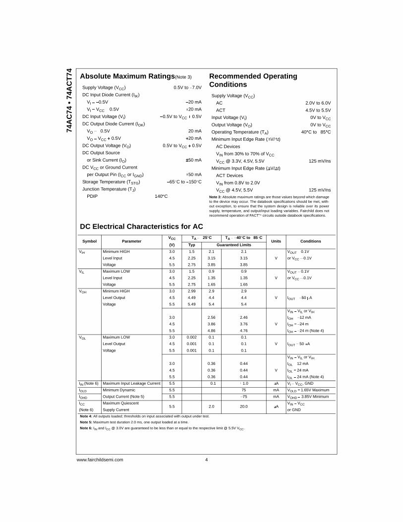
www.fairchildsemi.com 4
74A
C74
• 7
4AC
T74 Absolute Maximum Ratings(Note 3) Recommended Operating
Conditions
Note 3: Absolute maximum ratings are those values beyond which damageto the device may occur. The databook specifications should be met, with-out exception, to ensure that the system design is reliable over its powersupply, temperature, and output/input loading variables. Fairchild does notrecommend operation of FACT¥ circuits outside databook specifications.
DC Electrical Characteristics for AC
Note 4: All outputs loaded; thresholds on input associated with output under test.
Note 5: Maximum test duration 2.0 ms, one output loaded at a time.
Note 6: IIN and ICC @ 3.0V are guaranteed to be less than or equal to the respective limit @ 5.5V VCC.
Supply Voltage (VCC) 0.5V to 7.0V
DC Input Diode Current (IIK)
VI 0.5V 20 mA
VI VCC 0.5V 20 mA
DC Input Voltage (VI) 0.5V to VCC 0.5V
DC Output Diode Current (IOK)
VO 0.5V 20 mA
VO VCC 0.5V 20 mA
DC Output Voltage (VO) 0.5V to VCC 0.5V
DC Output Source
or Sink Current (IO) r50 mA
DC VCC or Ground Current
per Output Pin (ICC or IGND) r50 mA
Storage Temperature (TSTG) 65qC to 150qC
Junction Temperature (TJ)
PDIP 140qC
Supply Voltage (VCC)
AC 2.0V to 6.0V
ACT 4.5V to 5.5V
Input Voltage (VI) 0V to VCC
Output Voltage (VO) 0V to VCC
Operating Temperature (TA) 40qC to 85qC
Minimum Input Edge Rate ('V/'t)
AC Devices
VIN from 30% to 70% of VCC
VCC @ 3.3V, 4.5V, 5.5V 125 mV/ns
Minimum Input Edge Rate ('V/'t)
ACT Devices
VIN from 0.8V to 2.0V
VCC @ 4.5V, 5.5V 125 mV/ns
Symbol ParameterVCC TA 25qC TA 40qC to 85qC
Units Conditions(V) Typ Guaranteed Limits
VIH Minimum HIGH 3.0 1.5 2.1 2.1 VOUT 0.1V
Level Input 4.5 2.25 3.15 3.15 V or VCC 0.1V
Voltage 5.5 2.75 3.85 3.85
VIL Maximum LOW 3.0 1.5 0.9 0.9 VOUT 0.1V
Level Input 4.5 2.25 1.35 1.35 V or VCC 0.1V
Voltage 5.5 2.75 1.65 1.65
VOH Minimum HIGH 3.0 2.99 2.9 2.9
Level Output 4.5 4.49 4.4 4.4 V IOUT 50 PA
Voltage 5.5 5.49 5.4 5.4
VIN VIL or VIH
3.0 2.56 2.46 IOH 12 mA
4.5 3.86 3.76 V IOH 24 m
5.5 4.86 4.76 IOH 24 m (Note 4)
VOL Maximum LOW 3.0 0.002 0.1 0.1
Level Output 4.5 0.001 0.1 0.1 V IOUT 50 PA
Voltage 5.5 0.001 0.1 0.1
VIN VIL or VIH
3.0 0.36 0.44 IOL 12 mA
4.5 0.36 0.44 V IOL 24 mA
5.5 0.36 0.44 IOL 24 mA (Note 4)
IIN (Note 6) Maximum Input Leakage Current 5.5 r 0.1 r 1.0 PA VI VCC, GND
IOLD Minimum Dynamic 5.5 75 mA VOLD 1.65V Maximum
IOHD Output Current (Note 5) 5.5 75 mA VOHD 3.85V Minimum
ICC Maximum Quiescent5.5 2.0 20.0 PA
VIN VCC
(Note 6) Supply Current or GND
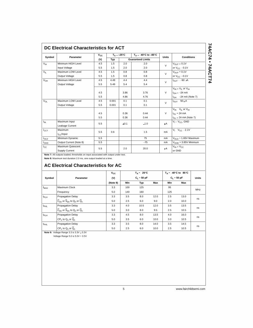
5 www.fairchildsemi.com
74AC
74 • 74AC
T74
DC Electrical Characteristics for ACT
Note 7: All outputs loaded; thresholds on input associated with output under test.
Note 8: Maximum test duration 2.0 ms, one output loaded at a time.
AC Electrical Characteristics for AC
Note 9: Voltage Range 3.3 is 3.3V r 0.3V
Voltage Range 5.0 is 5.0V r 0.5V
Symbol ParameterVCC TA 25qC TA 40qC to 85qC
Units Conditions(V) Typ Guaranteed Limits
VIH Minimum HIGH Level 4.5 1.5 2.0 2.0V
VOUT 0.1V
Input Voltage 5.5 1.5 2.0 2.0 or VCC 0.1V
VIL Maximum LOW Level 4.5 1.5 0.8 0.8V
VOUT 0.1V
Output Voltage 5.5 1.5 0.8 0.8 or VCC 0.1V
VOH Minimum HIGH Level 4.5 4.49 4.4 4.4V
IOUT 50 PA
Output Voltage 5.5 5.49 5.4 5.4
VIN VIL or VIH
4.5 3.86 3.76 V IOH 24 mA
5.5 4.86 4.76 IOH 24 mA (Note 7)
VOL Maximum LOW Level 4.5 0.001 0.1 0.1V
IOUT 50 PA
Output Voltage 5.5 0.001 0.1 0.1
VIN VIL or VIH
4.5 0.36 0.44 V IOL 24 mA
5.5 0.36 0.44 IOL 24 mA (Note 7)
IIN Maximum Input5.5 r0.1 r1.0 PA
VI VCC, GND
Leakage Current
ICCT Maximum5.5 0.6 1.5 mA
VI VCC 2.1V
ICC/Input
IOLD Minimum Dynamic 5.5 75 mA VOLD 1.65V Maximum
IOHD Output Current (Note 8) 5.5 75 mA VOHD 3.85V Minimum
ICC Maximum Quiescent5.5 2.0 20.0 PA
VIN VCC
Supply Current or GND
VCC TA 25qC TA 40qC to 85qC
Symbol Parameter (V) CL 50 pF CL 50 pF Units
(Note 9) Min Typ Max Min Max
fMAX Maximum Clock 3.3 100 125 95MHz
Frequency 5.0 140 160 125
tPLH Propagation Delay 3.3 3.5 8.0 12.0 2.5 13.0ns
CDn or SDn to Qn or Qn 5.0 2.5 6.0 9.0 2.0 10.0
tPHL Propagation Delay 3.3 4.0 10.5 12.0 3.5 13.5ns
CDn or SDn to Qn or Qn 5.0 3.0 8.0 9.5 2.5 10.5
tPLH Propagation Delay 3.3 4.5 8.0 13.5 4.0 16.0ns
CPn to Qn or Qn 5.0 3.5 6.0 10.0 3.0 10.5
tPHL Propagation Delay 3.3 3.5 8.0 14.0 3.5 14.5ns
CPn to Qn or Qn 5.0 2.5 6.0 10.0 2.5 10.5

www.fairchildsemi.com 6
74A
C74
• 7
4AC
T74 AC Operating Requirements for AC
Note 10: Voltage Range 3.3 is 3.3V r 0.3V
Voltage Range 5.0 is 5.0V r 0.5V
AC Electrical Characteristics for ACT
Note 11: Voltage Range 5.0 is 5.0V r 0.5V
AC Operating Requirements for ACT
Note 12: Voltage Range 5.0 is 5.0V r 0.5V
Capacitance
VCC TA 25qC TA 40qC to 85qC
Symbol Parameter (V) CL 50 pF CL 50 pF Units
(Note 10) Typ Guaranteed Minimum
tS Set-up Time, HIGH or LOW 3.3 1.5 4.0 4.5ns
Dn to CPn 5.0 1.0 3.0 3.0
tH Hold Time, HIGH or LOW 3.3 2.0 0.5 0.5ns
Dn to CPn 5.0 1.5 0.5 0.5
tW CPn or CDn or SDn 3.3 3.0 5.5 7.0ns
Pulse Width 5.0 2.5 4.5 5.0
trec Recovery Time 3.3 2.5 0 0ns
CDn or SDn to CP 5.0 2.0 0 0
VCC TA 25qC TA 40qC to 85qC
Symbol Parameter (V) CL 50 pF CL 50 pF Units
(Note 11) Min Typ Max Min Max
fMAX Maximum Clock5.0 145 210 125 MHz
Frequency
tPLH Propagation Delay 5.0 3.0 5.5 9.5 2.5 10.5 ns
CDn or SDn to Qn or Qn
tPHL Propagation Delay 5.0 3.0 6.0 10.0 3.0 11.5 ns
CDn or SDn to Qn or Qn
tPLH Propagation Delay 5.0 4.0 7.5 11.0 4.0 13.0. ns
CPn to Qn or Qn
tPHL Propagation Delay 5.0 3.5 6.0 10.0 3.0 11.5 ns
CPn to Qn or Qn
VCC TA 25qC TA 40qC to 85qC
Symbol Parameter (V) CL 50 pF CL 50 pF Units
(Note 12) Typ Guaranteed Minimum
tS Set-up Time, HIGH or LOW5.0 1.0 3.0 3.5 ns
Dn to CPn
tH Hold Time, HIGH or LOW5.0 0.5 1.0 1.0 ns
Dn to CPn
tW CPn or CDn or SDn5.0 3.0 5.0 6.0 ns
Pulse Width
trec Recovery Time 5.0 2.5 0 0 ns
CDn or SDn to CP
Symbol Parameter Typ Units Conditions
CIN Input Capacitance 4.5 pF VCC OPEN
CPD Power Dissipation Capacitance 35.0 pF VCC 5.0V

7 www.fairchildsemi.com
74AC
74 • 74AC
T74
Physical Dimensions inches (millimeters) unless otherwise noted
14-Lead Small Outline Integrated Circuit (SOIC), JEDEC MS-012, 0.150" NarrowPackage Number M14A

www.fairchildsemi.com 8
74A
C74
• 7
4AC
T74 Physical Dimensions inches (millimeters) unless otherwise noted (Continued)
Pb-Free 14-Lead Small Outline Package (SOP), EIAJ TYPE II, 5.3mm WidePackage Number M14D

9 www.fairchildsemi.com
74AC
74 • 74AC
T74
Physical Dimensions inches (millimeters) unless otherwise noted (Continued)
14-Lead Thin Shrink Small Outline Package (TSSOP), JEDEC MO-153, 4.4mm WidePackage Number MTC14

www.fairchildsemi.com 10
74A
C74
• 7
4AC
T74
Du
al D
-Typ
e P
osi
tive
Ed
ge-
Trig
ger
ed F
lip-F
lop
Physical Dimensions inches (millimeters) unless otherwise noted (Continued)
14-Lead Plastic Dual-In-Line Package (PDIP), JEDEC MS-001, 0.300" WidePackage Number N14A
Fairchild does not assume any responsibility for use of any circuitry described, no circuit patent licenses are implied andFairchild reserves the right at any time without notice to change said circuitry and specifications.
LIFE SUPPORT POLICY
FAIRCHILD’S PRODUCTS ARE NOT AUTHORIZED FOR USE AS CRITICAL COMPONENTS IN LIFE SUPPORTDEVICES OR SYSTEMS WITHOUT THE EXPRESS WRITTEN APPROVAL OF THE PRESIDENT OF FAIRCHILDSEMICONDUCTOR CORPORATION. As used herein:
1. Life support devices or systems are devices or systemswhich, (a) are intended for surgical implant into thebody, or (b) support or sustain life, and (c) whose failureto perform when properly used in accordance withinstructions for use provided in the labeling, can be rea-sonably expected to result in a significant injury to theuser.
2. A critical component in any component of a life supportdevice or system whose failure to perform can be rea-sonably expected to cause the failure of the life supportdevice or system, or to affect its safety or effectiveness.
www.fairchildsemi.com

3. SN74AHCT14: Hex Schmitt-Trigger Inverter
Texas Instruments Hex Schmitt-Trigger Inverter
SN74AHCT14
F -22
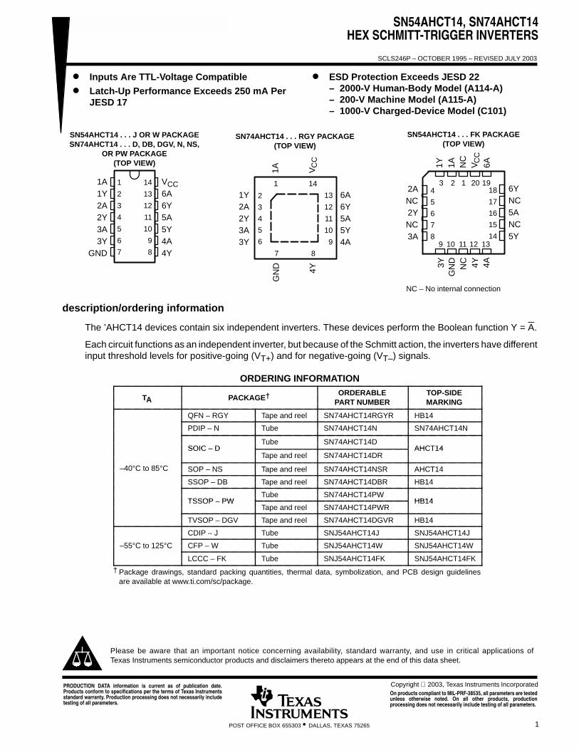
SN54AHCT14, SN74AHCT14HEX SCHMITT-TRIGGER INVERTERS
SCLS246P – OCTOBER 1995 – REVISED JULY 2003
1POST OFFICE BOX 655303 • DALLAS, TEXAS 75265
Inputs Are TTL-Voltage Compatible
Latch-Up Performance Exceeds 250 mA PerJESD 17
ESD Protection Exceeds JESD 22– 2000-V Human-Body Model (A114-A)– 200-V Machine Model (A115-A)– 1000-V Charged-Device Model (C101)
1
2
3
4
5
6
7
14
13
12
11
10
9
8
1A1Y2A2Y3A3Y
GND
VCC6A6Y5A5Y4A4Y
SN54AHCT14 . . . J OR W PACKAGESN74AHCT14 . . . D, DB, DGV, N, NS,
OR PW PACKAGE(TOP VIEW)
3 2 1 20 19
9 10 11 12 13
4
5
6
7
8
18
17
16
15
14
6YNC5ANC5Y
2ANC2YNC3A
1Y 1A NC
4Y 4AV 6A
3YG
ND
NC
SN54AHCT14 . . . FK PACKAGE(TOP VIEW)
CC
NC – No internal connection
SN74AHCT14 . . . RGY PACKAGE(TOP VIEW)
1 14
7 8
2
3
4
5
6
13
12
11
10
9
6A6Y5A5Y4A
1Y2A2Y3A3Y
1A
4YV
GN
D
CC
description/ordering information
The ’AHCT14 devices contain six independent inverters. These devices perform the Boolean function Y = A.
Each circuit functions as an independent inverter, but because of the Schmitt action, the inverters have differentinput threshold levels for positive-going (VT+) and for negative-going (VT–) signals.
ORDERING INFORMATION
TA PACKAGE† ORDERABLEPART NUMBER
TOP-SIDEMARKING
QFN – RGY Tape and reel SN74AHCT14RGYR HB14
PDIP – N Tube SN74AHCT14N SN74AHCT14N
SOIC – DTube SN74AHCT14D
AHCT14SOIC – DTape and reel SN74AHCT14DR
AHCT14
–40°C to 85°C SOP – NS Tape and reel SN74AHCT14NSR AHCT14
SSOP – DB Tape and reel SN74AHCT14DBR HB14
TSSOP PWTube SN74AHCT14PW
HB14TSSOP – PWTape and reel SN74AHCT14PWR
HB14
TVSOP – DGV Tape and reel SN74AHCT14DGVR HB14
CDIP – J Tube SNJ54AHCT14J SNJ54AHCT14J
–55°C to 125°C CFP – W Tube SNJ54AHCT14W SNJ54AHCT14W
LCCC – FK Tube SNJ54AHCT14FK SNJ54AHCT14FK
† Package drawings, standard packing quantities, thermal data, symbolization, and PCB design guidelinesare available at www.ti.com/sc/package.
PRODUCTION DATA information is current as of publication date.Products conform to specifications per the terms of Texas Instrumentsstandard warranty. Production processing does not necessarily includetesting of all parameters.
Copyright 2003, Texas Instruments Incorporated
Please be aware that an important notice concerning availability, standard warranty, and use in critical applications ofTexas Instruments semiconductor products and disclaimers thereto appears at the end of this data sheet.
On products compliant to MIL-PRF-38535, all parameters are testedunless otherwise noted. On all other products, productionprocessing does not necessarily include testing of all parameters.

SN54AHCT14, SN74AHCT14HEX SCHMITT-TRIGGER INVERTERS
SCLS246P – OCTOBER 1995 – REVISED JULY 2003
2 POST OFFICE BOX 655303 • DALLAS, TEXAS 75265
FUNCTION TABLE(each inverter)
INPUTA
OUTPUTY
H L
L H
logic diagram, each inverter (positive logic)
YA
absolute maximum ratings over operating free-air temperature range (unless otherwise noted)†
Supply voltage range, VCC –0.5 V to 7 V. . . . . . . . . . . . . . . . . . . . . . . . . . . . . . . . . . . . . . . . . . . . . . . . . . . . . . . . . . Input voltage range, VI (see Note 1) –0.5 V to 7 V. . . . . . . . . . . . . . . . . . . . . . . . . . . . . . . . . . . . . . . . . . . . . . . . . . Output voltage range, VO (see Note 1) –0.5 V to VCC + 0.5 V. . . . . . . . . . . . . . . . . . . . . . . . . . . . . . . . . . . . . . . . Input clamp current, IIK (VI < 0) –20 mA. . . . . . . . . . . . . . . . . . . . . . . . . . . . . . . . . . . . . . . . . . . . . . . . . . . . . . . . . . . Output clamp current, IOK (VO < 0 or VO > VCC) ±20 mA. . . . . . . . . . . . . . . . . . . . . . . . . . . . . . . . . . . . . . . . . . . . Continuous output current, IO (VO = 0 to VCC) ±25 mA. . . . . . . . . . . . . . . . . . . . . . . . . . . . . . . . . . . . . . . . . . . . . . Continuous current through VCC or GND ±50 mA. . . . . . . . . . . . . . . . . . . . . . . . . . . . . . . . . . . . . . . . . . . . . . . . . . . Package thermal impedance, θJA (see Note 2): D package 86°C/W. . . . . . . . . . . . . . . . . . . . . . . . . . . . . . . . . . .
(see Note 2): DB package 96°C/W. . . . . . . . . . . . . . . . . . . . . . . . . . . . . . . . . (see Note 2): DGV package 127°C/W. . . . . . . . . . . . . . . . . . . . . . . . . . . . . . . (see Note 2): N package 80°C/W. . . . . . . . . . . . . . . . . . . . . . . . . . . . . . . . . . . (see Note 2): NS package 76°C/W. . . . . . . . . . . . . . . . . . . . . . . . . . . . . . . . . (see Note 2): PW package 113°C/W. . . . . . . . . . . . . . . . . . . . . . . . . . . . . . . . (see Note 3): RGY package 47°C/W. . . . . . . . . . . . . . . . . . . . . . . . . . . . . . . .
Storage temperature range, Tstg –65°C to 150°C. . . . . . . . . . . . . . . . . . . . . . . . . . . . . . . . . . . . . . . . . . . . . . . . . . .
† Stresses beyond those listed under “absolute maximum ratings” may cause permanent damage to the device. These are stress ratings only, andfunctional operation of the device at these or any other conditions beyond those indicated under “recommended operating conditions” is notimplied. Exposure to absolute-maximum-rated conditions for extended periods may affect device reliability.
NOTES: 1. The input and output voltage ratings may be exceeded if the input and output current ratings are observed.2. The package thermal impedance is calculated in accordance with JESD 51-7.3. The package thermal impedance is calculated in accordance with JESD 51-5.
recommended operating conditions (see Note 4)
SN54AHCT14 SN74AHCT14UNIT
MIN MAX MIN MAXUNIT
VCC Supply voltage 4.5 5.5 4.5 5.5 V
VI Input voltage 0 5.5 0 5.5 V
VO Output voltage 0 VCC 0 VCC V
IOH High-level output current –8 –8 mA
IOL Low-level output current 8 8 mA
TA Operating free-air temperature –55 125 –40 85 °C
NOTE 4: All unused inputs of the device must be held at VCC or GND to ensure proper device operation. Refer to the TI application report,Implications of Slow or Floating CMOS Inputs, literature number SCBA004.

SN54AHCT14, SN74AHCT14HEX SCHMITT-TRIGGER INVERTERS
SCLS246P – OCTOBER 1995 – REVISED JULY 2003
3POST OFFICE BOX 655303 • DALLAS, TEXAS 75265
electrical characteristics over recommended operating free-air temperature range (unlessotherwise noted)
PARAMETER TEST CONDITIONS VCCTA = 25°C SN54AHCT14 SN74AHCT14
UNITPARAMETER TEST CONDITIONS VCCMIN TYP MAX MIN MAX MIN MAX
UNIT
VT+Positive going input
4.5 V 0.9 1.9 0.9 1.9 0.9 1.9VPositive-going input
threshold voltage 5.5 V 1 2.1 1 2.1 1 2.1V
VT–Negative going input
4.5 V 0.5 1.5 0.5 1.5 0.5 1.5VNegative-going input
threshold voltage 5.5 V 0.6 1.7 0.6 1.7 0.6 1.7V
∆VTHysteresis
4.5 V 0.4 1.4 0.4 1.4 0.4 1.4VHysteresis
(VT+ – VT–) 5.5 V 0.4 1.5 0.4 1.5 0.4 1.5V
VOHIOH = –50 A 4.5 V 4.4 4.5 4.4 4.4
VVOHIOH = –8 mA 4.5 V 3.94 3.8 3.8
V
VOLIOL = 50 A 4.5 V 0.1 0.1 0.1
VVOLIOL = 8 mA 4.5 V 0.36 0.44 0.44
V
II VI = 5.5 V or GND 0 V to 5.5 V ±0.1 ±1* ±1 A
ICC VI = VCC or GND, IO = 0 5.5 V 2 20 20 A
∆ICC† One input at 3.4 V,Other inputs at VCC or GND
5.5 V 1.35 1.5 1.5 mA
Ci VI = VCC or GND 5 V 2 10 10 pF
* On products compliant to MIL-PRF-38535, this parameter is not production tested at VCC = 0 V.† This is the increase in supply current for each input at one of the specified TTL voltage levels, rather than 0 V or VCC.
switching characteristics over recommended operating free-air temperature range VCC = 5 V ± 0.5 V (unless otherwise noted) (see Figure 1)
PARAMETERFROM TO LOAD TA = 25°C SN54AHCT14 SN74AHCT14
UNITPARAMETER(INPUT) (OUTPUT) CAPACITANCE MIN TYP MAX MIN MAX MIN MAX
UNIT
tPLHA Y CL = 15 pF
4** 7** 1** 8** 1 8ns
tPHLA Y CL = 15 pF
4** 7** 1** 8** 1 8ns
tPLHA Y CL = 50 pF
5.5 8 1 9 1 9ns
tPHLA Y CL = 50 pF
5.5 8 1 9 1 9ns
** On products compliant to MIL-PRF-38535, this parameter is not production tested.
noise characteristics, VCC = 5 V, CL = 50 pF, TA = 25°C (see Note 5)
PARAMETERSN74AHCT14
UNITPARAMETERMIN TYP MAX
UNIT
VOL(P) Quiet output, maximum dynamic VOL 0.9 V
VOL(V) Quiet output, minimum dynamic VOL –0.7 V
VOH(V) Quiet output, minimum dynamic VOH 4.3 V
VIH(D) High-level dynamic input voltage 2.1 V
VIL(D) Low-level dynamic input voltage 0.5 V
NOTE 5: Characteristics are for surface-mount packages only.
operating characteristics, VCC = 5 V, TA = 25°CPARAMETER TEST CONDITIONS TYP UNIT
Cpd Power dissipation capacitance No load, f = 1 MHz 12 pF
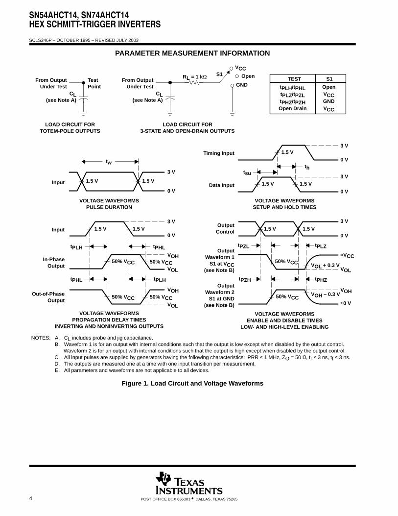
SN54AHCT14, SN74AHCT14HEX SCHMITT-TRIGGER INVERTERS
SCLS246P – OCTOBER 1995 – REVISED JULY 2003
4 POST OFFICE BOX 655303 • DALLAS, TEXAS 75265
PARAMETER MEASUREMENT INFORMATION
50% VCC
3 V
3 V
0 V
0 V
thtsu
VOLTAGE WAVEFORMSSETUP AND HOLD TIMES
Data Input
tPLH
tPHL
tPHL
tPLH
VOH
VOH
VOL
VOL
3 V
0 V
50% VCC50% VCC
Input
Out-of-PhaseOutput
In-PhaseOutput
Timing Input
50% VCC
VOLTAGE WAVEFORMSPROPAGATION DELAY TIMES
INVERTING AND NONINVERTING OUTPUTS
OutputControl
OutputWaveform 1
S1 at VCC(see Note B)
OutputWaveform 2
S1 at GND(see Note B)
VOL
VOH
tPZL
tPZH
tPLZ
tPHZ
≈VCC
0 V
50% VCC VOL + 0.3 V
50% VCC≈0 V
3 V
VOLTAGE WAVEFORMSENABLE AND DISABLE TIMES
LOW- AND HIGH-LEVEL ENABLING
tPLH/tPHLtPLZ/tPZLtPHZ/tPZHOpen Drain
OpenVCCGNDVCC
TEST S1
3 V
0 V
tw
VOLTAGE WAVEFORMSPULSE DURATION
Input
NOTES: A. CL includes probe and jig capacitance.B. Waveform 1 is for an output with internal conditions such that the output is low except when disabled by the output control.
Waveform 2 is for an output with internal conditions such that the output is high except when disabled by the output control.C. All input pulses are supplied by generators having the following characteristics: PRR ≤ 1 MHz, ZO = 50 Ω, tr ≤ 3 ns, tf ≤ 3 ns.D. The outputs are measured one at a time with one input transition per measurement.E. All parameters and waveforms are not applicable to all devices.
From OutputUnder Test
CL(see Note A)
LOAD CIRCUIT FOR3-STATE AND OPEN-DRAIN OUTPUTS
S1VCC
RL = 1 kΩGND
From OutputUnder Test
CL(see Note A)
TestPoint
LOAD CIRCUIT FORTOTEM-POLE OUTPUTS
Open
VOH – 0.3 V
1.5 V 1.5 V
1.5 V
1.5 V 1.5 V
1.5 V 1.5 V1.5 V 1.5 V
Figure 1. Load Circuit and Voltage Waveforms


MECHANICAL DATA
MCFP002A – JANUARY 1995 – REVISED FEBRUARY 2002
1POST OFFICE BOX 655303 • DALLAS, TEXAS 75265
W (R-GDFP-F14) CERAMIC DUAL FLATPACK
0.360 (9,14)0.250 (6,35)
87
141
0.235 (5,97)
0.004 (0,10)
0.026 (0,66)
4 Places
0.015 (0,38)
0.045 (1,14)
0.335 (8,51)
0.008 (0,20)
0.045 (1,14)
Base and Seating Plane
0.005 (0,13) MIN
0.019 (0,48)
0.390 (9,91)
0.260 (6,60)
0.080 (2,03)
4040180-2/C 02/02
0.360 (9,14)0.250 (6,35)
0.280 (7,11) MAX
0.050 (1,27)
NOTES: A. All linear dimensions are in inches (millimeters).B. This drawing is subject to change without notice.C. This package can be hermetically sealed with a ceramic lid using glass frit.D. Index point is provided on cap for terminal identification only.E. Falls within MIL STD 1835 GDFP1-F14 and JEDEC MO-092AB

MECHANICAL DATA
MLCC006B – OCTOBER 1996
1POST OFFICE BOX 655303 • DALLAS, TEXAS 75265
FK (S-CQCC-N**) LEADLESS CERAMIC CHIP CARRIER
4040140/D 10/96
28 TERMINAL SHOWN
B
0.358(9,09)
MAX
(11,63)
0.560(14,22)
0.560
0.458
0.858(21,8)
1.063(27,0)
(14,22)
ANO. OF
MINMAX
0.358
0.660
0.761
0.458
0.342(8,69)
MIN
(11,23)
(16,26)0.640
0.739
0.442
(9,09)
(11,63)
(16,76)
0.962
1.165
(23,83)0.938
(28,99)1.141
(24,43)
(29,59)
(19,32)(18,78)
**
20
28
52
44
68
84
0.020 (0,51)
TERMINALS
0.080 (2,03)0.064 (1,63)
(7,80)0.307
(10,31)0.406
(12,58)0.495
(12,58)0.495
(21,6)0.850
(26,6)1.047
0.045 (1,14)
0.045 (1,14)0.035 (0,89)
0.035 (0,89)
0.010 (0,25)
121314151618 17
11
10
8
9
7
5
432
0.020 (0,51)0.010 (0,25)
6
12826 27
19
21B SQ
A SQ22
23
24
25
20
0.055 (1,40)0.045 (1,14)
0.028 (0,71)0.022 (0,54)
0.050 (1,27)
NOTES: A. All linear dimensions are in inches (millimeters).B. This drawing is subject to change without notice.C. This package can be hermetically sealed with a metal lid.D. The terminals are gold plated.E. Falls within JEDEC MS-004
MPDI002C – JANUARY 1995 – REVISED DECEMBER 20002
1POST OFFICE BOX 655303 • DALLAS, TEXAS 75265
N (R-PDIP-T**) PLASTIC DUAL-IN-LINE PACKAGE
BB AC AD
0.325 (8,26)0.300 (7,62)
0.010 (0,25) NOM
Gauge Plane
0.015 (0,38)
0.430 (10,92) MAX
20
1.060(26,92)
0.940(23,88)
18
0.920
0.850
14
0.775
0.745
(19,69)
(18,92)
16
0.775(19,69)
(18,92)0.745
A MIN
DIM
A MAX
PINS **
(23,37)
(21,59)
Seating Plane
14/18 PIN ONLY20 pin vendor option
4040049/E 12/2002
9
80.070 (1,78)
A
0.045 (1,14)0.020 (0,51) MIN
16
1
0.015 (0,38)0.021 (0,53)
0.200 (5,08) MAX
0.125 (3,18) MIN
0.240 (6,10)0.260 (6,60)
M0.010 (0,25)
0.100 (2,54)
16 PINS SHOWN
MS-100VARIATION
AAC
D
D
D0.030 (0,76)
0.045 (1,14)
NOTES: A. All linear dimensions are in inches (millimeters).B. This drawing is subject to change without notice.
C. Falls within JEDEC MS-001, except 18 and 20 pin minimum body lrngth (Dim A).
D. The 20 pin end lead shoulder width is a vendor option, either half or full width.
MECHANICAL DATA
MPDS006C – FEBRUARY 1996 – REVISED AUGUST 2000
1POST OFFICE BOX 655303 • DALLAS, TEXAS 75265
DGV (R-PDSO-G**) PLASTIC SMALL-OUTLINE 24 PINS SHOWN
14
3,70
3,50 4,90
5,10
20DIM
PINS **
4073251/E 08/00
1,20 MAX
Seating Plane
0,050,15
0,25
0,500,75
0,230,13
1 12
24 13
4,304,50
0,16 NOM
Gage Plane
A
7,90
7,70
382416
4,90
5,103,70
3,50
A MAX
A MIN
6,606,20
11,20
11,40
56
9,60
9,80
48
0,08
M0,070,40
0°–8°
NOTES: A. All linear dimensions are in millimeters.B. This drawing is subject to change without notice.C. Body dimensions do not include mold flash or protrusion, not to exceed 0,15 per side.D. Falls within JEDEC: 24/48 Pins – MO-153
14/16/20/56 Pins – MO-194

MECHANICAL DATA
MSOI002B – JANUARY 1995 – REVISED SEPTEMBER 2001
1POST OFFICE BOX 655303 • DALLAS, TEXAS 75265
D (R-PDSO-G**) PLASTIC SMALL-OUTLINE PACKAGE8 PINS SHOWN
8
0.197(5,00)
A MAX
A MIN(4,80)0.189 0.337
(8,55)
(8,75)0.344
14
0.386(9,80)
(10,00)0.394
16DIM
PINS **
4040047/E 09/01
0.069 (1,75) MAX
Seating Plane
0.004 (0,10)0.010 (0,25)
0.010 (0,25)
0.016 (0,40)0.044 (1,12)
0.244 (6,20)0.228 (5,80)
0.020 (0,51)0.014 (0,35)
1 4
8 5
0.150 (3,81)0.157 (4,00)
0.008 (0,20) NOM
0°– 8°
Gage Plane
A
0.004 (0,10)
0.010 (0,25)0.050 (1,27)
NOTES: A. All linear dimensions are in inches (millimeters).B. This drawing is subject to change without notice.C. Body dimensions do not include mold flash or protrusion, not to exceed 0.006 (0,15).D. Falls within JEDEC MS-012


MECHANICAL DATA
MSSO002E – JANUARY 1995 – REVISED DECEMBER 2001
1POST OFFICE BOX 655303 • DALLAS, TEXAS 75265
DB (R-PDSO-G**) PLASTIC SMALL-OUTLINE
4040065 /E 12/01
28 PINS SHOWN
Gage Plane
8,207,40
0,550,95
0,25
38
12,90
12,30
28
10,50
24
8,50
Seating Plane
9,907,90
30
10,50
9,90
0,38
5,605,00
15
0,22
14
A
28
1
2016
6,506,50
14
0,05 MIN
5,905,90
DIM
A MAX
A MIN
PINS **
2,00 MAX
6,90
7,50
0,65 M0,15
0°–8°
0,10
0,090,25
NOTES: A. All linear dimensions are in millimeters.B. This drawing is subject to change without notice.C. Body dimensions do not include mold flash or protrusion not to exceed 0,15.D. Falls within JEDEC MO-150

MECHANICAL DATA
MTSS001C – JANUARY 1995 – REVISED FEBRUARY 1999
1POST OFFICE BOX 655303 • DALLAS, TEXAS 75265
PW (R-PDSO-G**) PLASTIC SMALL-OUTLINE PACKAGE14 PINS SHOWN
0,65 M0,10
0,10
0,25
0,500,75
0,15 NOM
Gage Plane
28
9,80
9,60
24
7,90
7,70
2016
6,60
6,40
4040064/F 01/97
0,30
6,606,20
8
0,19
4,304,50
7
0,15
14
A
1
1,20 MAX
14
5,10
4,90
8
3,10
2,90
A MAX
A MIN
DIMPINS **
0,05
4,90
5,10
Seating Plane
0°–8°
NOTES: A. All linear dimensions are in millimeters.B. This drawing is subject to change without notice.C. Body dimensions do not include mold flash or protrusion not to exceed 0,15.D. Falls within JEDEC MO-153

IMPORTANT NOTICE
Texas Instruments Incorporated and its subsidiaries (TI) reserve the right to make corrections, modifications,enhancements, improvements, and other changes to its products and services at any time and to discontinueany product or service without notice. Customers should obtain the latest relevant information before placingorders and should verify that such information is current and complete. All products are sold subject to TI’s termsand conditions of sale supplied at the time of order acknowledgment.
TI warrants performance of its hardware products to the specifications applicable at the time of sale inaccordance with TI’s standard warranty. Testing and other quality control techniques are used to the extent TIdeems necessary to support this warranty. Except where mandated by government requirements, testing of allparameters of each product is not necessarily performed.
TI assumes no liability for applications assistance or customer product design. Customers are responsible fortheir products and applications using TI components. To minimize the risks associated with customer productsand applications, customers should provide adequate design and operating safeguards.
TI does not warrant or represent that any license, either express or implied, is granted under any TI patent right,copyright, mask work right, or other TI intellectual property right relating to any combination, machine, or processin which TI products or services are used. Information published by TI regarding third-party products or servicesdoes not constitute a license from TI to use such products or services or a warranty or endorsement thereof.Use of such information may require a license from a third party under the patents or other intellectual propertyof the third party, or a license from TI under the patents or other intellectual property of TI.
Reproduction of information in TI data books or data sheets is permissible only if reproduction is withoutalteration and is accompanied by all associated warranties, conditions, limitations, and notices. Reproductionof this information with alteration is an unfair and deceptive business practice. TI is not responsible or liable forsuch altered documentation.
Resale of TI products or services with statements different from or beyond the parameters stated by TI for thatproduct or service voids all express and any implied warranties for the associated TI product or service andis an unfair and deceptive business practice. TI is not responsible or liable for any such statements.
Following are URLs where you can obtain information on other Texas Instruments products and applicationsolutions:
Products Applications
Amplifiers amplifier.ti.com Audio www.ti.com/audio
Data Converters dataconverter.ti.com Automotive www.ti.com/automotive
DSP dsp.ti.com Broadband www.ti.com/broadband
Interface interface.ti.com Digital Control www.ti.com/digitalcontrol
Logic logic.ti.com Military www.ti.com/military
Power Mgmt power.ti.com Optical Networking www.ti.com/opticalnetwork
Microcontrollers microcontroller.ti.com Security www.ti.com/security
Telephony www.ti.com/telephony
Video & Imaging www.ti.com/video
Wireless www.ti.com/wireless
Mailing Address: Texas Instruments
Post Office Box 655303 Dallas, Texas 75265
Copyright 2003, Texas Instruments Incorporated

4. SN74ALS08: Quadruple 2-Input Positive-AND Gates
Texas Instruments Quadruple 2-Input Positive-AND Gates
SN74ALS08
F -38

SN54ALS08, SN54AS08, SN74ALS08, SN74AS08 QUADRUPLE 2-INPUT POSITIVE-AND GATES
SDAS191A – APRIL 1982 – REVISED DECEMBER 1994
Copyright 1994, Texas Instruments Incorporated
1POST OFFICE BOX 655303 • DALLAS, TEXAS 75265
• Package Options Include PlasticSmall-Outline (D) Packages, Ceramic ChipCarriers (FK), and Standard Plastic (N) andCeramic (J) 300-mil DIPs
description
These devices contain four independent 2-inputpositive-AND gates. They perform the Booleanfunctions Y = A • B or Y = A + B in positive logic.
The SN54ALS08 and SN54AS08 arecharacterized for operation over the full militarytemperature range of –55°C to 125°C. TheSN74ALS08 and SN74AS08 are characterized foroperation from 0°C to 70°C.
FUNCTION TABLE (each gate)
INPUTS OUTPUTA B Y
H H H
L X L
X L L
logic symbol † logic diagram (positive logic)
11A
21B
42A
52B
93A
103B
124A
134B
&1Y
3
2Y6
3Y8
4Y11
11A
21B
1Y3
42A
52B
2Y6
93A
103B
3Y8
124A
134B
4Y11
† This symbol is in accordance with ANSI/IEEE Std 91-1984 andIEC Publication 617-12.
Pin numbers shown are for the D, J, and N packages.
SN54ALS08, SN54AS08 . . . J PACKAGESN74ALS08, SN74AS08 . . . D OR N PACKAGE
(TOP VIEW)
1
2
3
4
5
6
7
14
13
12
11
10
9
8
1A1B1Y2A2B2Y
GND
VCC4B4A4Y3B3A3Y
SN54ALS08, SN54AS08 . . . FK PACKAGE(TOP VIEW)
3 2 1 20 19
9 10 11 12 13
4
5
6
7
8
18
17
16
15
14
4ANC4YNC3B
1YNC2ANC2B
1B 1A NC
3Y 3A
V 4B
2Y NC
CC
NC – No internal connection
GN
D
PRODUCTION DATA information is current as of publication date.Products conform to specifications per the terms of Texas Instrumentsstandard warranty. Production processing does not necessarily includetesting of all parameters.
SN54ALS08, SN54AS08, SN74ALS08, SN74AS08QUADRUPLE 2-INPUT POSITIVE-AND GATES SDAS191A – APRIL 1982 – REVISED DECEMBER 1994
2 POST OFFICE BOX 655303 • DALLAS, TEXAS 75265
absolute maximum ratings over operating free-air temperature range (unless otherwise noted) †
Supply voltage, VCC 7 V. . . . . . . . . . . . . . . . . . . . . . . . . . . . . . . . . . . . . . . . . . . . . . . . . . . . . . . . . . . . . . . . . . . . . . . . Input voltage, VI 7 V. . . . . . . . . . . . . . . . . . . . . . . . . . . . . . . . . . . . . . . . . . . . . . . . . . . . . . . . . . . . . . . . . . . . . . . . . . . . Operating free-air temperature range, TA: SN54ALS08 –55°C to 125°C. . . . . . . . . . . . . . . . . . . . . . . . . . . . . .
SN74ALS08 0°C to 70°C. . . . . . . . . . . . . . . . . . . . . . . . . . . . . . . . . . Storage temperature range –65°C to 150°C. . . . . . . . . . . . . . . . . . . . . . . . . . . . . . . . . . . . . . . . . . . . . . . . . . . . . . .
† Stresses beyond those listed under “absolute maximum ratings” may cause permanent damage to the device. These are stress ratings only, andfunctional operation of the device at these or any other conditions beyond those indicated under “recommended operating conditions” is notimplied. Exposure to absolute-maximum-rated conditions for extended periods may affect device reliability.
recommended operating conditions
SN54ALS08 SN74ALS08UNIT
MIN NOM MAX MIN NOM MAXUNIT
VCC Supply voltage 4.5 5 5.5 4.5 5 5.5 V
VIH High-level input voltage 2 2 V
VIL Low level input voltage0.8‡ 0.8
VVIL Low-level input voltage0.7§
V
IOH High-level output current –0.4 –0.4 mA
IOL Low-level output current 4 8 mA
TA Operating free-air temperature –55 125 0 70 °C‡ Applies over temperature range –55°C to 70°C§ Applies over temperature range 70°C to 125°C
electrical characteristics over recommended operating free-air temperature range (unlessotherwise noted)
PARAMETER TEST CONDITIONSSN54ALS08 SN74ALS08
UNITPARAMETER TEST CONDITIONSMIN TYP¶ MAX MIN TYP¶ MAX
UNIT
VIK VCC = 4.5 V, II = –18 mA –1.5 –1.5 V
VOH VCC = 4.5 V to 5.5 V, IOH = –0.4 mA VCC –2 VCC –2 V
VOL VCC = 4 5 VIOL = 4 mA 0.25 0.4 0.25 0.4
VVOL VCC = 4.5 VIOL = 8 mA 0.35 0.5
V
II VCC = 5.5 V, VI = 7 V 0.1 0.1 mA
IIH VCC = 5.5 V, VI = 2.7 V 20 20 µA
IIL VCC = 5.5 V, VI = 0.4 V –0.1 –0.1 mA
IO# VCC = 5.5 V, VO = 2.25 V –20 –112 –30 –112 mA
ICCH VCC = 5.5 V, VI = 4.5 V 1.3 2.4 1.3 2.4 mA
ICCL VCC = 5.5 V, VI = 0 2.2 4 2.2 4 mA
¶ All typical values are at VCC = 5 V, TA = 25°C.# The output conditions have been chosen to produce a current that closely approximates one half of the true short-circuit output current, IOS.
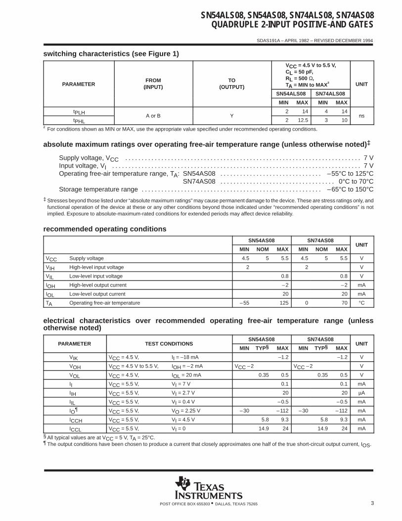
SN54ALS08, SN54AS08, SN74ALS08, SN74AS08 QUADRUPLE 2-INPUT POSITIVE-AND GATES
SDAS191A – APRIL 1982 – REVISED DECEMBER 1994
3POST OFFICE BOX 655303 • DALLAS, TEXAS 75265
switching characteristics (see Figure 1)
PARAMETERFROM
(INPUT)TO
(OUTPUT)
VCC = 4.5 V to 5.5 V,CL = 50 pF,RL = 500 Ω,TA = MIN to MAX † UNIT(INPUT) (OUTPUT)
SN54ALS08 SN74ALS08
MIN MAX MIN MAX
tPLHA or B Y
2 14 4 14ns
tPHLA or B Y
2 12.5 3 10ns
† For conditions shown as MIN or MAX, use the appropriate value specified under recommended operating conditions.
absolute maximum ratings over operating free-air temperature range (unless otherwise noted) ‡
Supply voltage, VCC 7 V. . . . . . . . . . . . . . . . . . . . . . . . . . . . . . . . . . . . . . . . . . . . . . . . . . . . . . . . . . . . . . . . . . . . . . . . Input voltage, VI 7 V. . . . . . . . . . . . . . . . . . . . . . . . . . . . . . . . . . . . . . . . . . . . . . . . . . . . . . . . . . . . . . . . . . . . . . . . . . . . Operating free-air temperature range, TA: SN54AS08 –55°C to 125°C. . . . . . . . . . . . . . . . . . . . . . . . . . . . . . .
SN74AS08 0°C to 70°C. . . . . . . . . . . . . . . . . . . . . . . . . . . . . . . . . . . Storage temperature range –65°C to 150°C. . . . . . . . . . . . . . . . . . . . . . . . . . . . . . . . . . . . . . . . . . . . . . . . . . . . . . .
‡ Stresses beyond those listed under “absolute maximum ratings” may cause permanent damage to the device. These are stress ratings only, andfunctional operation of the device at these or any other conditions beyond those indicated under “recommended operating conditions” is notimplied. Exposure to absolute-maximum-rated conditions for extended periods may affect device reliability.
recommended operating conditions
SN54AS08 SN74AS08UNIT
MIN NOM MAX MIN NOM MAXUNIT
VCC Supply voltage 4.5 5 5.5 4.5 5 5.5 V
VIH High-level input voltage 2 2 V
VIL Low-level input voltage 0.8 0.8 V
IOH High-level output current –2 –2 mA
IOL Low-level output current 20 20 mA
TA Operating free-air temperature –55 125 0 70 °C
electrical characteristics over recommended operating free-air temperature range (unlessotherwise noted)
PARAMETER TEST CONDITIONSSN54AS08 SN74AS08
UNITPARAMETER TEST CONDITIONSMIN TYP§ MAX MIN TYP§ MAX
UNIT
VIK VCC = 4.5 V, II = –18 mA –1.2 –1.2 V
VOH VCC = 4.5 V to 5.5 V, IOH = –2 mA VCC –2 VCC –2 V
VOL VCC = 4.5 V, IOL = 20 mA 0.35 0.5 0.35 0.5 V
II VCC = 5.5 V, VI = 7 V 0.1 0.1 mA
IIH VCC = 5.5 V, VI = 2.7 V 20 20 µA
IIL VCC = 5.5 V, VI = 0.4 V –0.5 –0.5 mA
IO¶ VCC = 5.5 V, VO = 2.25 V –30 –112 –30 –112 mA
ICCH VCC = 5.5 V, VI = 4.5 V 5.8 9.3 5.8 9.3 mA
ICCL VCC = 5.5 V, VI = 0 14.9 24 14.9 24 mA
§ All typical values are at VCC = 5 V, TA = 25°C.¶ The output conditions have been chosen to produce a current that closely approximates one half of the true short-circuit output current, IOS.

SN54ALS08, SN54AS08, SN74ALS08, SN74AS08QUADRUPLE 2-INPUT POSITIVE-AND GATES SDAS191A – APRIL 1982 – REVISED DECEMBER 1994
4 POST OFFICE BOX 655303 • DALLAS, TEXAS 75265
switching characteristics (see Figure 1)
PARAMETERFROM
(INPUT)TO
(OUTPUT)
VCC = 4.5 V to 5.5 V,CL = 50 pF,RL = 500 Ω,TA = MIN to MAX † UNIT(INPUT) (OUTPUT)
SN54AS08 SN74AS08
MIN MAX MIN MAX
tPLHA or B Y
1 6.5 1 5.5ns
tPHLA or B Y
1 6.5 1 5.5ns
† For conditions shown as MIN or MAX, use the appropriate value specified under recommended operating conditions.
SN54ALS08, SN54AS08, SN74ALS08, SN74AS08 QUADRUPLE 2-INPUT POSITIVE-AND GATES
SDAS191A – APRIL 1982 – REVISED DECEMBER 1994
5POST OFFICE BOX 655303 • DALLAS, TEXAS 75265
PARAMETER MEASUREMENT INFORMATIONSERIES 54ALS/74ALS AND 54AS/74AS DEVICES
tPHZ
tPLZ
tPHLtPLH
0.3 V
tPZL
tPZH
tPLHtPHL
LOAD CIRCUITFOR 3-STATE OUTPUTS
From OutputUnder Test
Test Point
R1
S1
CL(see Note A)
7 V
1.3 V
1.3 V1.3 V
3.5 V
3.5 V
0.3 V
0.3 V
thtsu
VOLTAGE WAVEFORMSSETUP AND HOLD TIMES
TimingInput
DataInput
1.3 V 1.3 V3.5 V
3.5 V
0.3 V
0.3 V
High-LevelPulse
Low-LevelPulse
tw
VOLTAGE WAVEFORMSPULSE DURATIONS
Input
Out-of-PhaseOutput
(see Note C)
1.3 V 1.3 V
1.3 V1.3 V
1.3 V 1.3 V
1.3 V1.3 V
1.3 V
1.3 V
3.5 V
3.5 V
0.3 V
0.3 V
VOL
VOH
VOH
VOL
OutputControl
(low-levelenabling)
Waveform 1S1 Closed
(see Note B)
Waveform 2S1 Open
(see Note B)0 V
VOH
VOL
3.5 V
In-PhaseOutput
0.3 V
1.3 V 1.3 V
VOLTAGE WAVEFORMSPROPAGATION DELAY TIMES
VOLTAGE WAVEFORMSENABLE AND DISABLE TIMES, 3-STATE OUTPUTS
R2
VCC
RL
Test Point
From OutputUnder Test
CL(see Note A)
LOAD CIRCUITFOR OPEN-COLLECTOR OUTPUTS
LOAD CIRCUIT FOR BI-STATE
TOTEM-POLE OUTPUTS
From OutputUnder Test
Test Point
CL(see Note A)
RL
RL = R1 = R2
NOTES: A. CL includes probe and jig capacitance.B. Waveform 1 is for an output with internal conditions such that the output is low except when disabled by the output control.
Waveform 2 is for an output with internal conditions such that the output is high except when disabled by the output control.C. When measuring propagation delay items of 3-state outputs, switch S1 is open.D. All input pulses have the following characteristics: PRR ≤ 1 MHz, tr = tf = 2 ns, duty cycle = 50%.E. The outputs are measured one at a time with one transition per measurement.
Figure 1. Load Circuits and Voltage Waveforms
PACKAGING INFORMATION
Orderable Device Status (1) PackageType
PackageDrawing
Pins PackageQty
Eco Plan (2) Lead/Ball Finish MSL Peak Temp (3)
5962-86842012A ACTIVE LCCC FK 20 1 TBD POST-PLATE N / A for Pkg Type
5962-8684201CA ACTIVE CDIP J 14 1 TBD A42 SNPB N / A for Pkg Type
5962-8684201DA ACTIVE CFP W 14 1 TBD A42 N / A for Pkg Type
JM38510/37401B2A ACTIVE LCCC FK 20 1 TBD POST-PLATE N / A for Pkg Type
JM38510/37401BCA ACTIVE CDIP J 14 1 TBD A42 SNPB N / A for Pkg Type
SN54ALS08J ACTIVE CDIP J 14 1 TBD A42 SNPB N / A for Pkg Type
SN54AS08J ACTIVE CDIP J 14 1 TBD A42 SNPB N / A for Pkg Type
SN74ALS08D ACTIVE SOIC D 14 50 Green (RoHS &no Sb/Br)
CU NIPDAU Level-1-260C-UNLIM
SN74ALS08DE4 ACTIVE SOIC D 14 50 Green (RoHS &no Sb/Br)
CU NIPDAU Level-1-260C-UNLIM
SN74ALS08DG4 ACTIVE SOIC D 14 50 Green (RoHS &no Sb/Br)
CU NIPDAU Level-1-260C-UNLIM
SN74ALS08DR ACTIVE SOIC D 14 2500 Green (RoHS &no Sb/Br)
CU NIPDAU Level-1-260C-UNLIM
SN74ALS08DRE4 ACTIVE SOIC D 14 2500 Green (RoHS &no Sb/Br)
CU NIPDAU Level-1-260C-UNLIM
SN74ALS08DRG4 ACTIVE SOIC D 14 2500 Green (RoHS &no Sb/Br)
CU NIPDAU Level-1-260C-UNLIM
SN74ALS08N ACTIVE PDIP N 14 25 Pb-Free(RoHS)
CU NIPDAU N / A for Pkg Type
SN74ALS08N3 OBSOLETE PDIP N 14 TBD Call TI Call TI
SN74ALS08NE4 ACTIVE PDIP N 14 25 Pb-Free(RoHS)
CU NIPDAU N / A for Pkg Type
SN74ALS08NSR ACTIVE SO NS 14 2000 Green (RoHS &no Sb/Br)
CU NIPDAU Level-1-260C-UNLIM
SN74ALS08NSRE4 ACTIVE SO NS 14 2000 Green (RoHS &no Sb/Br)
CU NIPDAU Level-1-260C-UNLIM
SN74AS08D ACTIVE SOIC D 14 50 Green (RoHS &no Sb/Br)
CU NIPDAU Level-1-260C-UNLIM
SN74AS08DE4 ACTIVE SOIC D 14 50 Green (RoHS &no Sb/Br)
CU NIPDAU Level-1-260C-UNLIM
SN74AS08DR ACTIVE SOIC D 14 2500 Green (RoHS &no Sb/Br)
CU NIPDAU Level-1-260C-UNLIM
SN74AS08DRE4 ACTIVE SOIC D 14 2500 Green (RoHS &no Sb/Br)
CU NIPDAU Level-1-260C-UNLIM
SN74AS08N ACTIVE PDIP N 14 25 Pb-Free(RoHS)
CU NIPDAU N / A for Pkg Type
SN74AS08N3 OBSOLETE PDIP N 14 TBD Call TI Call TI
SN74AS08NE4 ACTIVE PDIP N 14 25 Pb-Free(RoHS)
CU NIPDAU N / A for Pkg Type
SN74AS08NSR ACTIVE SO NS 14 2000 Green (RoHS &no Sb/Br)
CU NIPDAU Level-1-260C-UNLIM
SN74AS08NSRE4 ACTIVE SO NS 14 2000 Green (RoHS &no Sb/Br)
CU NIPDAU Level-1-260C-UNLIM
SNJ54ALS08FK ACTIVE LCCC FK 20 1 TBD POST-PLATE N / A for Pkg Type
SNJ54ALS08J ACTIVE CDIP J 14 1 TBD A42 SNPB N / A for Pkg Type
PACKAGE OPTION ADDENDUM
www.ti.com 6-Dec-2006
Addendum-Page 1

Orderable Device Status (1) PackageType
PackageDrawing
Pins PackageQty
Eco Plan (2) Lead/Ball Finish MSL Peak Temp (3)
SNJ54ALS08W ACTIVE CFP W 14 1 TBD A42 N / A for Pkg Type
SNJ54AS08FK ACTIVE LCCC FK 20 1 TBD POST-PLATE N / A for Pkg Type
SNJ54AS08J ACTIVE CDIP J 14 1 TBD A42 SNPB N / A for Pkg Type
SNJ54AS08W ACTIVE CFP W 14 1 TBD A42 N / A for Pkg Type
(1) The marketing status values are defined as follows:ACTIVE: Product device recommended for new designs.LIFEBUY: TI has announced that the device will be discontinued, and a lifetime-buy period is in effect.NRND: Not recommended for new designs. Device is in production to support existing customers, but TI does not recommend using this part ina new design.PREVIEW: Device has been announced but is not in production. Samples may or may not be available.OBSOLETE: TI has discontinued the production of the device.
(2) Eco Plan - The planned eco-friendly classification: Pb-Free (RoHS), Pb-Free (RoHS Exempt), or Green (RoHS & no Sb/Br) - please checkhttp://www.ti.com/productcontent for the latest availability information and additional product content details.TBD: The Pb-Free/Green conversion plan has not been defined.Pb-Free (RoHS): TI's terms "Lead-Free" or "Pb-Free" mean semiconductor products that are compatible with the current RoHS requirementsfor all 6 substances, including the requirement that lead not exceed 0.1% by weight in homogeneous materials. Where designed to be solderedat high temperatures, TI Pb-Free products are suitable for use in specified lead-free processes.Pb-Free (RoHS Exempt): This component has a RoHS exemption for either 1) lead-based flip-chip solder bumps used between the die andpackage, or 2) lead-based die adhesive used between the die and leadframe. The component is otherwise considered Pb-Free (RoHScompatible) as defined above.Green (RoHS & no Sb/Br): TI defines "Green" to mean Pb-Free (RoHS compatible), and free of Bromine (Br) and Antimony (Sb) based flameretardants (Br or Sb do not exceed 0.1% by weight in homogeneous material)
(3) MSL, Peak Temp. -- The Moisture Sensitivity Level rating according to the JEDEC industry standard classifications, and peak soldertemperature.
Important Information and Disclaimer:The information provided on this page represents TI's knowledge and belief as of the date that it isprovided. TI bases its knowledge and belief on information provided by third parties, and makes no representation or warranty as to theaccuracy of such information. Efforts are underway to better integrate information from third parties. TI has taken and continues to takereasonable steps to provide representative and accurate information but may not have conducted destructive testing or chemical analysis onincoming materials and chemicals. TI and TI suppliers consider certain information to be proprietary, and thus CAS numbers and other limitedinformation may not be available for release.
In no event shall TI's liability arising out of such information exceed the total purchase price of the TI part(s) at issue in this document sold by TIto Customer on an annual basis.
PACKAGE OPTION ADDENDUM
www.ti.com 6-Dec-2006
Addendum-Page 2


MECHANICAL DATA
MLCC006B – OCTOBER 1996
POST OFFICE BOX 655303 • DALLAS, TEXAS 75265
FK (S-CQCC-N**) LEADLESS CERAMIC CHIP CARRIER
4040140/D 10/96
28 TERMINAL SHOWN
B
0.358(9,09)
MAX
(11,63)
0.560(14,22)
0.560
0.458
0.858(21,8)
1.063(27,0)
(14,22)
ANO. OF
MINMAX
0.358
0.660
0.761
0.458
0.342(8,69)
MIN
(11,23)
(16,26)0.640
0.739
0.442
(9,09)
(11,63)
(16,76)
0.962
1.165
(23,83)0.938
(28,99)1.141
(24,43)
(29,59)
(19,32)(18,78)
**
20
28
52
44
68
84
0.020 (0,51)
TERMINALS
0.080 (2,03)0.064 (1,63)
(7,80)0.307
(10,31)0.406
(12,58)0.495
(12,58)0.495
(21,6)0.850
(26,6)1.047
0.045 (1,14)
0.045 (1,14)0.035 (0,89)
0.035 (0,89)
0.010 (0,25)
121314151618 17
11
10
8
9
7
5
432
0.020 (0,51)0.010 (0,25)
6
12826 27
19
21B SQ
A SQ22
23
24
25
20
0.055 (1,40)0.045 (1,14)
0.028 (0,71)0.022 (0,54)
0.050 (1,27)
NOTES: A. All linear dimensions are in inches (millimeters).B. This drawing is subject to change without notice.C. This package can be hermetically sealed with a metal lid.D. The terminals are gold plated.E. Falls within JEDEC MS-004

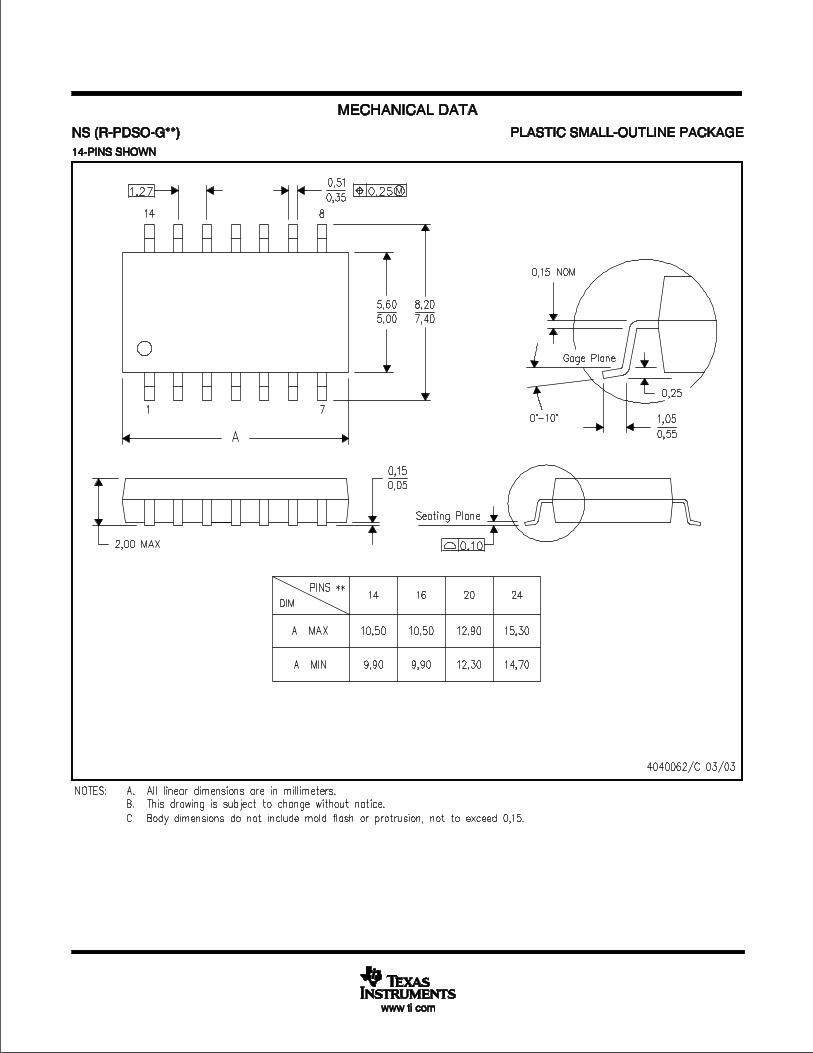

IMPORTANT NOTICE
Texas Instruments Incorporated and its subsidiaries (TI) reserve the right to make corrections, modifications,enhancements, improvements, and other changes to its products and services at any time and to discontinueany product or service without notice. Customers should obtain the latest relevant information before placingorders and should verify that such information is current and complete. All products are sold subject to TI’s termsand conditions of sale supplied at the time of order acknowledgment.
TI warrants performance of its hardware products to the specifications applicable at the time of sale inaccordance with TI’s standard warranty. Testing and other quality control techniques are used to the extent TIdeems necessary to support this warranty. Except where mandated by government requirements, testing of allparameters of each product is not necessarily performed.
TI assumes no liability for applications assistance or customer product design. Customers are responsible fortheir products and applications using TI components. To minimize the risks associated with customer productsand applications, customers should provide adequate design and operating safeguards.
TI does not warrant or represent that any license, either express or implied, is granted under any TI patent right,copyright, mask work right, or other TI intellectual property right relating to any combination, machine, or processin which TI products or services are used. Information published by TI regarding third-party products or servicesdoes not constitute a license from TI to use such products or services or a warranty or endorsement thereof.Use of such information may require a license from a third party under the patents or other intellectual propertyof the third party, or a license from TI under the patents or other intellectual property of TI.
Reproduction of information in TI data books or data sheets is permissible only if reproduction is withoutalteration and is accompanied by all associated warranties, conditions, limitations, and notices. Reproductionof this information with alteration is an unfair and deceptive business practice. TI is not responsible or liable forsuch altered documentation.
Resale of TI products or services with statements different from or beyond the parameters stated by TI for thatproduct or service voids all express and any implied warranties for the associated TI product or service andis an unfair and deceptive business practice. TI is not responsible or liable for any such statements.
Following are URLs where you can obtain information on other Texas Instruments products and applicationsolutions:
Products Applications
Amplifiers amplifier.ti.com Audio www.ti.com/audio
Data Converters dataconverter.ti.com Automotive www.ti.com/automotive
DSP dsp.ti.com Broadband www.ti.com/broadband
Interface interface.ti.com Digital Control www.ti.com/digitalcontrol
Logic logic.ti.com Military www.ti.com/military
Power Mgmt power.ti.com Optical Networking www.ti.com/opticalnetwork
Microcontrollers microcontroller.ti.com Security www.ti.com/security
Low Power Wireless www.ti.com/lpw Telephony www.ti.com/telephony
Video & Imaging www.ti.com/video
Wireless www.ti.com/wireless
Mailing Address: Texas Instruments
Post Office Box 655303 Dallas, Texas 75265
Copyright 2006, Texas Instruments Incorporated
5. SN74HCT74: Dual D-Type Positive-Edge-Triggered Flip Flops
Texas Instruments Dual D-Type Positive-Edge-Triggered
Flip Flops with Clear and Preset SN74HCT74
F -53

SN54HCT74, SN74HCT74DUAL D-TYPE POSITIVE-EDGE-TRIGGERED FLIP-FLOPS
WITH CLEAR AND PRESETSCLS169D – DECEMBER 1982 – REVISED AUGUST 2003
1POST OFFICE BOX 655303 • DALLAS, TEXAS 75265
Operating Voltage Range of 4.5 V to 5.5 V
Outputs Can Drive Up To 10 LSTTL Loads
Low Power Consumption, 40-µA Max ICC Typical tpd = 17 ns
±4-mA Output Drive at 5 V
Low Input Current of 1 µA Max
Inputs Are TTL-Voltage Compatible
description/ordering information
The ’HCT74 devices contain two independentD-type positive-edge-triggered flip-flops. A lowlevel at the preset (PRE) or clear (CLR) inputs setsor resets the outputs, regardless of the levels ofthe other inputs. When PRE and CLR are inactive(high), data at the data (D) input meeting the setuptime requirements are transferred to the outputson the positive-going edge of the clock (CLK)pulse. Clock triggering occurs at a voltage leveland is not directly related to the rise time of CLK.Following the hold-time interval, data at theD input may be changed without affecting thelevels at the outputs.
ORDERING INFORMATION
TA PACKAGE† ORDERABLEPART NUMBER
TOP-SIDEMARKING
–40 C to 85 C
PDIP – N Tube of 25 SN74HCT74N SN74HCT74N
–40 C to 85 C
SOIC – D
Tube of 50 SN74HCT74D
HCT74
–40 C to 85 C
SOIC – D Reel of 2500 SN74HCT74DR HCT74
–40 C to 85 C
Reel of 250 SN74HCT74DT
–40°C to 85°C SOP – NS Reel of 2000 SN74HCT74NSR HCT74
SSOP – DB Reel of 2000 SN74HCT74DBR HT74
TSSOP – PW
Tube of 90 SN74HCT74PW
HT74TSSOP – PW Reel of 2000 SN74HCT74PWR HT74
Reel of 250 SN74HCT74PWT
–55 C to 125 C
CDIP – J Tube of 25 SNJ54HCT74J SNJ54HCT74J
–55°C to 125°C CFP – W Tube of 150 SNJ54HCT74W SNJ54HCT74W
LCCC – FK Tube of 55 SNJ54HCT74FK SNJ54HCT74FK† Package drawings, standard packing quantities, thermal data, symbolization, and PCB design guidelines are
available at www.ti.com/sc/package.
Please be aware that an important notice concerning availability, standard warranty, and use in critical applications ofTexas Instruments semiconductor products and disclaimers thereto appears at the end of this data sheet.
1
2
3
4
5
6
7
14
13
12
11
10
9
8
1CLR1D
1CLK1PRE
1Q1Q
GND
VCC2CLR2D2CLK2PRE2Q2Q
SN54HCT74 . . . J OR W PACKAGESN74HCT74 . . . D, DB, N, NS, OR PW PACKAGE
(TOP VIEW)
3 2 1 20 19
9 10 11 12 13
4
5
6
7
8
18
17
16
15
14
2DNC2CLKNC2PRE
1CLKNC
1PRENC1Q
1D 1CLR
NC
2Q 2QV 2C
LR
1QG
ND
NC
SN54HCT74 . . . FK PACKAGE(TOP VIEW)
CC
NC – No internal connection
Copyright 2003, Texas Instruments IncorporatedUNLESS OTHERWISE NOTED this document contains PRODUCTIONDATA information current as of publication date. Products conform tospecifications per the terms of Texas Instruments standard warranty.Production processing does not necessarily include testing of allparameters.
SN54HCT74, SN74HCT74DUAL D-TYPE POSITIVE-EDGE-TRIGGERED FLIP-FLOPSWITH CLEAR AND PRESET
SCLS169D – DECEMBER 1982 – REVISED AUGUST 2003
2 POST OFFICE BOX 655303 • DALLAS, TEXAS 75265
FUNCTION TABLE
INPUTS OUTPUT
PRE CLR CLK D Q Q
L H X X H L
H L X X L H
L L X X H† H†
H H H H L
H H L L H
H H L X Q0 Q0† This configuration is nonstable; that is, it does not
persist when PRE or CLR returns to its inactive(high) level.
logic diagram (positive logic)
PRE
CLK
D
CLR
Q
Q
C
C
C
C
C
C
C
C
C
C
TG
TG TG TG
absolute maximum ratings over operating free-air temperature range (unless otherwise noted)‡
Supply voltage range, VCC –0.5 V to 7 V. . . . . . . . . . . . . . . . . . . . . . . . . . . . . . . . . . . . . . . . . . . . . . . . . . . . . . . . . . Input clamp current, IIK (VI < 0 or VI > VCC) (see Note 1) ±20 mA. . . . . . . . . . . . . . . . . . . . . . . . . . . . . . . . . . . . Output clamp current, IOK (VO < 0 or VO > VCC) (see Note 1) ±20 mA. . . . . . . . . . . . . . . . . . . . . . . . . . . . . . . . Continuous output current, IO (VO = 0 to VCC) ±25 mA. . . . . . . . . . . . . . . . . . . . . . . . . . . . . . . . . . . . . . . . . . . . . . Continuous current through VCC or GND ±50 mA. . . . . . . . . . . . . . . . . . . . . . . . . . . . . . . . . . . . . . . . . . . . . . . . . . . Package thermal impedance, θJA (see Note 2): D package 86°C/W. . . . . . . . . . . . . . . . . . . . . . . . . . . . . . . . . . .
DB package 96°C/W. . . . . . . . . . . . . . . . . . . . . . . . . . . . . . . . . N package 80°C/W. . . . . . . . . . . . . . . . . . . . . . . . . . . . . . . . . . . NS package 76°C/W. . . . . . . . . . . . . . . . . . . . . . . . . . . . . . . . . PW package 113°C/W. . . . . . . . . . . . . . . . . . . . . . . . . . . . . . . .
Storage temperature range, Tstg –65°C to 150°C. . . . . . . . . . . . . . . . . . . . . . . . . . . . . . . . . . . . . . . . . . . . . . . . . . .
‡ Stresses beyond those listed under “absolute maximum ratings” may cause permanent damage to the device. These are stress ratings only, andfunctional operation of the device at these or any other conditions beyond those indicated under “recommended operating conditions” is notimplied. Exposure to absolute-maximum-rated conditions for extended periods may affect device reliability.
NOTES: 1. The input and output voltage ratings may be exceeded if the input and output current ratings are observed.2. The package thermal impedance is calculated in accordance with JESD 51-7.
SN54HCT74, SN74HCT74DUAL D-TYPE POSITIVE-EDGE-TRIGGERED FLIP-FLOPS
WITH CLEAR AND PRESETSCLS169D – DECEMBER 1982 – REVISED AUGUST 2003
3POST OFFICE BOX 655303 • DALLAS, TEXAS 75265
recommended operating conditions (see Note 3)
SN54HCT74 SN74HCT74UNIT
MIN NOM MAX MIN NOM MAXUNIT
VCC Supply voltage 4.5 5 5.5 4.5 5 5.5 V
VIH High-level input voltage VCC = 4.5 V to 5.5 V 2 2 V
VIL Low-level input voltage VCC = 4.5 V to 5.5 V 0.8 0.8 V
VI Input voltage 0 VCC 0 VCC V
VO Output voltage 0 VCC 0 VCC V
∆t/∆v Input transition rise/fall time 500 500 ns
TA Operating free-air temperature –55 125 –40 85 °C
NOTE 3: All unused inputs of the device must be held at VCC or GND to ensure proper device operation. Refer to the TI application report,Implications of Slow or Floating CMOS Inputs, literature number SCBA004.
electrical characteristics over recommended operating free-air temperature range (unlessotherwise noted)
PARAMETER TEST CONDITIONS VCCTA = 25°C SN54HCT74 SN74HCT74
UNITPARAMETER TEST CONDITIONS VCCMIN TYP MAX MIN MAX MIN MAX
UNIT
VOH VI = VIH or VILIOH = –20 µA
4.5 V4.4 4.499 4.4 4.4
VVOH VI = VIH or VILIOH = –4 mA
4.5 V3.98 4.3 3.7 3.84
V
VOL VI = VIH or VILIOL = 20 µA
4.5 V0.001 0.1 0.1 0.1
VVOL VI = VIH or VILIOL = 4 mA
4.5 V0.17 0.26 0.4 0.33
V
II VI = VCC or 0 5.5 V ±0.1 ±100 ±1000 ±1000 nA
ICC VI = VCC or 0, IO = 0 5.5 V 4 80 40 µA
∆ICC† One input at 0.5 V or 2.4 V,Other inputs at 0 or VCC
5.5 V 1.4 2.4 3 2.9 mA
Ci4.5 V
to 5.5 V3 10 10 10 pF
† This is the increase in supply current for each input that is at one of the specified TTL voltage levels, rather than 0 V or VCC.
timing requirements over recommended operating free-air temperature range (unless otherwisenoted)
VCCTA = 25°C SN54HCT74 SN74HCT74
UNITVCCMIN MAX MIN MAX MIN MAX
UNIT
fclock Clock frequency4.5 V 27 18 22
MHzfclock Clock frequency5.5 V 30 20 24
MHz
t Pulse duration
PRE or CLR low4.5 V 16 24 20
nstw Pulse duration
PRE or CLR low5.5 V 14 21 18
nstw Pulse duration
CLK high or low4.5 V 18 27 23
ns
CLK high or low5.5 V 16 24 21
t Setup time before CLK↑
Data4.5 V 12 18 15
nstsu Setup time before CLK↑
Data5.5 V 11 16 14
nstsu Setup time before CLK↑
PRE or CLR inactive4.5 V 0 0 0
ns
PRE or CLR inactive5.5 V 0 0 0
th Hold time, data after CLK↑4.5 V 0 0 0
nsth Hold time, data after CLK↑5.5 V 0 0 0
ns
PRODUCT PREVIEW information concerns products in the formative ordesign phase of development. Characteristic data and otherspecifications are design goals. Texas Instruments reserves the right tochange or discontinue these products without notice.

SN54HCT74, SN74HCT74DUAL D-TYPE POSITIVE-EDGE-TRIGGERED FLIP-FLOPSWITH CLEAR AND PRESET
SCLS169D – DECEMBER 1982 – REVISED AUGUST 2003
4 POST OFFICE BOX 655303 • DALLAS, TEXAS 75265
switching characteristics over recommended operating free-air temperature range, CL = 50 pF(unless otherwise noted) (see Figure 1)
PARAMETERFROM TO
VCCTA = 25°C SN54HCT74 SN74HCT74
UNITPARAMETERFROM
(INPUT)TO
(OUTPUT)VCC
MIN TYP MAX MIN MAX MIN MAXUNIT
fmax4.5 V 27 40 18 22
MHzfmax5.5 V 30 46 20 24
MHz
t
PRE or CLR Q or Q4.5 V 21 35 53 44
nstpd
PRE or CLR Q or Q5.5 V 17 31 48 40
nstpdCLK Q or Q
4.5 V 20 28 42 35ns
CLK Q or Q5.5 V 18 25 38 31
tt Q or Q4.5 V 8 15 22 19
nstt Q or Q5.5 V 7 14 20 17
ns
operating characteristics, TA = 25°CPARAMETER TEST CONDITIONS TYP UNIT
Cpd Power dissipation capacitance per flip-flop No load 35 pF
PARAMETER MEASUREMENT INFORMATION
VOLTAGE WAVEFORMSSETUP AND HOLD AND INPUT RISE AND FALL TIMES
VOLTAGE WAVEFORMSPULSE DURATIONS
thtsu
1.3 V
1.3 V1.3 V0.3 V0.3 V
2.7 V 2.7 V
3 V
3 V
0 V
0 V
tr tf
ReferenceInput
DataInput
1.3 VHigh-Level
Pulse 1.3 V3 V
0 V
1.3 V 1.3 V
3 V
0 V
tw
Low-LevelPulse
VOLTAGE WAVEFORMSPROPAGATION DELAY AND OUTPUT RISE AND FALL TIMES
1.3 V
1.3 V1.3 V10%10%
90% 90%
3 V
VOH
VOL
0 V
tr tf
Input
In-PhaseOutput
1.3 V
tPLH tPHL
1.3 V 1.3 V10% 10%
90%90%VOH
VOLtrtf
tPHL tPLHOut-of-Phase
Output
TestPoint
From OutputUnder Test
CL = 50 pF(see Note A)
LOAD CIRCUIT
NOTES: A. CL includes probe and test-fixture capacitance.B. Phase relationships between waveforms were chosen arbitrarily. All input pulses are supplied by generators having the following
characteristics: PRR ≤ 1 MHz, ZO = 50 Ω, tr = 6 ns, tf = 6 ns.C. For clock inputs, fmax is measured when the input duty cycle is 50%.D. The outputs are measured one at a time with one input transition per measurement.E. tPLH and tPHL are the same as tpd.
Figure 1. Load Circuit and Voltage Waveforms
PRODUCT PREVIEW information concerns products in the formative ordesign phase of development. Characteristic data and otherspecifications are design goals. Texas Instruments reserves the right tochange or discontinue these products without notice.

MECHANICAL DATA
MCFP002A – JANUARY 1995 – REVISED FEBRUARY 2002
1POST OFFICE BOX 655303 • DALLAS, TEXAS 75265
W (R-GDFP-F14) CERAMIC DUAL FLATPACK
0.360 (9,14)0.250 (6,35)
87
141
0.235 (5,97)
0.004 (0,10)
0.026 (0,66)
4 Places
0.015 (0,38)
0.045 (1,14)
0.335 (8,51)
0.008 (0,20)
0.045 (1,14)
Base and Seating Plane
0.005 (0,13) MIN
0.019 (0,48)
0.390 (9,91)
0.260 (6,60)
0.080 (2,03)
4040180-2/C 02/02
0.360 (9,14)0.250 (6,35)
0.280 (7,11) MAX
0.050 (1,27)
NOTES: A. All linear dimensions are in inches (millimeters).B. This drawing is subject to change without notice.C. This package can be hermetically sealed with a ceramic lid using glass frit.D. Index point is provided on cap for terminal identification only.E. Falls within MIL STD 1835 GDFP1-F14 and JEDEC MO-092AB

MECHANICAL DATA
MLCC006B – OCTOBER 1996
1POST OFFICE BOX 655303 • DALLAS, TEXAS 75265
FK (S-CQCC-N**) LEADLESS CERAMIC CHIP CARRIER
4040140/D 10/96
28 TERMINAL SHOWN
B
0.358(9,09)
MAX
(11,63)
0.560(14,22)
0.560
0.458
0.858(21,8)
1.063(27,0)
(14,22)
ANO. OF
MINMAX
0.358
0.660
0.761
0.458
0.342(8,69)
MIN
(11,23)
(16,26)0.640
0.739
0.442
(9,09)
(11,63)
(16,76)
0.962
1.165
(23,83)0.938
(28,99)1.141
(24,43)
(29,59)
(19,32)(18,78)
**
20
28
52
44
68
84
0.020 (0,51)
TERMINALS
0.080 (2,03)0.064 (1,63)
(7,80)0.307
(10,31)0.406
(12,58)0.495
(12,58)0.495
(21,6)0.850
(26,6)1.047
0.045 (1,14)
0.045 (1,14)0.035 (0,89)
0.035 (0,89)
0.010 (0,25)
121314151618 17
11
10
8
9
7
5
432
0.020 (0,51)0.010 (0,25)
6
12826 27
19
21B SQ
A SQ22
23
24
25
20
0.055 (1,40)0.045 (1,14)
0.028 (0,71)0.022 (0,54)
0.050 (1,27)
NOTES: A. All linear dimensions are in inches (millimeters).B. This drawing is subject to change without notice.C. This package can be hermetically sealed with a metal lid.D. The terminals are gold plated.E. Falls within JEDEC MS-004

MPDI002C – JANUARY 1995 – REVISED DECEMBER 20002
1POST OFFICE BOX 655303 • DALLAS, TEXAS 75265
N (R-PDIP-T**) PLASTIC DUAL-IN-LINE PACKAGE
BB AC AD
0.325 (8,26)0.300 (7,62)
0.010 (0,25) NOM
Gauge Plane
0.015 (0,38)
0.430 (10,92) MAX
20
1.060(26,92)
0.940(23,88)
18
0.920
0.850
14
0.775
0.745
(19,69)
(18,92)
16
0.775(19,69)
(18,92)0.745
A MIN
DIM
A MAX
PINS **
(23,37)
(21,59)
Seating Plane
14/18 PIN ONLY20 pin vendor option
4040049/E 12/2002
9
80.070 (1,78)
A
0.045 (1,14)0.020 (0,51) MIN
16
1
0.015 (0,38)0.021 (0,53)
0.200 (5,08) MAX
0.125 (3,18) MIN
0.240 (6,10)0.260 (6,60)
M0.010 (0,25)
0.100 (2,54)
16 PINS SHOWN
MS-100VARIATION
AAC
D
D
D0.030 (0,76)
0.045 (1,14)
NOTES: A. All linear dimensions are in inches (millimeters).B. This drawing is subject to change without notice.
C. Falls within JEDEC MS-001, except 18 and 20 pin minimum body lrngth (Dim A).
D. The 20 pin end lead shoulder width is a vendor option, either half or full width.

MECHANICAL DATA
MSOI002B – JANUARY 1995 – REVISED SEPTEMBER 2001
1POST OFFICE BOX 655303 • DALLAS, TEXAS 75265
D (R-PDSO-G**) PLASTIC SMALL-OUTLINE PACKAGE8 PINS SHOWN
8
0.197(5,00)
A MAX
A MIN(4,80)0.189 0.337
(8,55)
(8,75)0.344
14
0.386(9,80)
(10,00)0.394
16DIM
PINS **
4040047/E 09/01
0.069 (1,75) MAX
Seating Plane
0.004 (0,10)0.010 (0,25)
0.010 (0,25)
0.016 (0,40)0.044 (1,12)
0.244 (6,20)0.228 (5,80)
0.020 (0,51)0.014 (0,35)
1 4
8 5
0.150 (3,81)0.157 (4,00)
0.008 (0,20) NOM
0°– 8°
Gage Plane
A
0.004 (0,10)
0.010 (0,25)0.050 (1,27)
NOTES: A. All linear dimensions are in inches (millimeters).B. This drawing is subject to change without notice.C. Body dimensions do not include mold flash or protrusion, not to exceed 0.006 (0,15).D. Falls within JEDEC MS-012


MECHANICAL DATA
MSSO002E – JANUARY 1995 – REVISED DECEMBER 2001
1POST OFFICE BOX 655303 • DALLAS, TEXAS 75265
DB (R-PDSO-G**) PLASTIC SMALL-OUTLINE
4040065 /E 12/01
28 PINS SHOWN
Gage Plane
8,207,40
0,550,95
0,25
38
12,90
12,30
28
10,50
24
8,50
Seating Plane
9,907,90
30
10,50
9,90
0,38
5,605,00
15
0,22
14
A
28
1
2016
6,506,50
14
0,05 MIN
5,905,90
DIM
A MAX
A MIN
PINS **
2,00 MAX
6,90
7,50
0,65 M0,15
0°–8°
0,10
0,090,25
NOTES: A. All linear dimensions are in millimeters.B. This drawing is subject to change without notice.C. Body dimensions do not include mold flash or protrusion not to exceed 0,15.D. Falls within JEDEC MO-150

MECHANICAL DATA
MTSS001C – JANUARY 1995 – REVISED FEBRUARY 1999
1POST OFFICE BOX 655303 • DALLAS, TEXAS 75265
PW (R-PDSO-G**) PLASTIC SMALL-OUTLINE PACKAGE14 PINS SHOWN
0,65 M0,10
0,10
0,25
0,500,75
0,15 NOM
Gage Plane
28
9,80
9,60
24
7,90
7,70
2016
6,60
6,40
4040064/F 01/97
0,30
6,606,20
8
0,19
4,304,50
7
0,15
14
A
1
1,20 MAX
14
5,10
4,90
8
3,10
2,90
A MAX
A MIN
DIMPINS **
0,05
4,90
5,10
Seating Plane
0°–8°
NOTES: A. All linear dimensions are in millimeters.B. This drawing is subject to change without notice.C. Body dimensions do not include mold flash or protrusion not to exceed 0,15.D. Falls within JEDEC MO-153

IMPORTANT NOTICE
Texas Instruments Incorporated and its subsidiaries (TI) reserve the right to make corrections, modifications,enhancements, improvements, and other changes to its products and services at any time and to discontinueany product or service without notice. Customers should obtain the latest relevant information before placingorders and should verify that such information is current and complete. All products are sold subject to TI’s termsand conditions of sale supplied at the time of order acknowledgment.
TI warrants performance of its hardware products to the specifications applicable at the time of sale inaccordance with TI’s standard warranty. Testing and other quality control techniques are used to the extent TIdeems necessary to support this warranty. Except where mandated by government requirements, testing of allparameters of each product is not necessarily performed.
TI assumes no liability for applications assistance or customer product design. Customers are responsible fortheir products and applications using TI components. To minimize the risks associated with customer productsand applications, customers should provide adequate design and operating safeguards.
TI does not warrant or represent that any license, either express or implied, is granted under any TI patent right,copyright, mask work right, or other TI intellectual property right relating to any combination, machine, or processin which TI products or services are used. Information published by TI regarding third-party products or servicesdoes not constitute a license from TI to use such products or services or a warranty or endorsement thereof.Use of such information may require a license from a third party under the patents or other intellectual propertyof the third party, or a license from TI under the patents or other intellectual property of TI.
Reproduction of information in TI data books or data sheets is permissible only if reproduction is withoutalteration and is accompanied by all associated warranties, conditions, limitations, and notices. Reproductionof this information with alteration is an unfair and deceptive business practice. TI is not responsible or liable forsuch altered documentation.
Resale of TI products or services with statements different from or beyond the parameters stated by TI for thatproduct or service voids all express and any implied warranties for the associated TI product or service andis an unfair and deceptive business practice. TI is not responsible or liable for any such statements.
Following are URLs where you can obtain information on other Texas Instruments products and applicationsolutions:
Products Applications
Amplifiers amplifier.ti.com Audio www.ti.com/audio
Data Converters dataconverter.ti.com Automotive www.ti.com/automotive
DSP dsp.ti.com Broadband www.ti.com/broadband
Interface interface.ti.com Digital Control www.ti.com/digitalcontrol
Logic logic.ti.com Military www.ti.com/military
Power Mgmt power.ti.com Optical Networking www.ti.com/opticalnetwork
Microcontrollers microcontroller.ti.com Security www.ti.com/security
Telephony www.ti.com/telephony
Video & Imaging www.ti.com/video
Wireless www.ti.com/wireless
Mailing Address: Texas Instruments
Post Office Box 655303 Dallas, Texas 75265
Copyright 2003, Texas Instruments Incorporated

6. SN74AHCT541: Octal Buffers/Drivers with 3-State Outputs
Texas Instruments Octal Buffers/Drivers with 3-State Outputs
SN74AHCT541
F -67

SN54AHCT541, SN74AHCT541OCTAL BUFFERS/DRIVERS
WITH 3-STATE OUTPUTS
SCLS269O – DECEMBER 1995 – REVISED JULY 2003
1POST OFFICE BOX 655303 • DALLAS, TEXAS 75265
Inputs Are TTL-Voltage Compatible
Latch-Up Performance Exceeds 250 mA PerJESD 17
ESD Protection Exceeds JESD 22– 2000-V Human-Body Model (A114-A)– 200-V Machine Model (A115-A)– 1000-V Charged-Device Model (C101)
description/ordering information
The ’AHCT541 octal buffers/drivers are ideal fordriving bus lines or buffer memory addressregisters. These devices feature inputs andoutputs on opposite sides of the package tofacilitate printed circuit board layout.
The 3-state control gate is a 2-input AND gate withactive-low inputs so that if either output-enable(OE1 or OE2) input is high, all correspondingoutputs are in the high-impedance state. Theoutputs provide noninverted data when they arenot in the high-impedance state.
To ensure the high-impedance state during powerup or power down, OE should be tied to VCCthrough a pullup resistor; the minimum value ofthe resistor is determined by the current-sinkingcapability of the driver.
ORDERING INFORMATION
TA PACKAGE† ORDERABLEPART NUMBER
TOP-SIDEMARKING
PDIP – N Tube SN74AHCT541N SN74AHCT541N
SOIC DWTube SN74AHCT541DW
AHCT541SOIC – DWTape and reel SN74AHCT541DWR
AHCT541
40°C to 85°CSOP – NS Tape and reel SN74AHCT541NSR AHCT541
–40°C to 85°CSSOP – DB Tape and reel SN74AHCT541DBR HB541
TSSOP PWTube SN74AHCT541PW
HB541TSSOP – PWTape and reel SN74AHCT541PWR
HB541
TVSOP – DGV Tape and reel SN74AHCT541DGVR HB541
CDIP – J Tube SNJ54AHCT541J SNJ54AHCT541J
–55°C to 125°C CFP – W Tube SNJ54AHCT541W SNJ54AHCT541W
LCCC – FK Tube SNJ54AHCT541FK SNJ54AHCT541FK
† Package drawings, standard packing quantities, thermal data, symbolization, and PCB design guidelinesare available at www.ti.com/sc/package.
Copyright 2003, Texas Instruments IncorporatedPRODUCTION DATA information is current as of publication date.Products conform to specifications per the terms of Texas Instrumentsstandard warranty. Production processing does not necessarily includetesting of all parameters.
Please be aware that an important notice concerning availability, standard warranty, and use in critical applications ofTexas Instruments semiconductor products and disclaimers thereto appears at the end of this data sheet.
1
2
3
4
5
6
7
8
9
10
20
19
18
17
16
15
14
13
12
11
OE1A1A2A3A4A5A6A7A8
GND
VCCOE2Y1Y2Y3Y4Y5Y6Y7Y8
SN54AHCT541 . . . J OR W PACKAGESN74AHCT541 . . . DB, DGV, DW, N, NS, OR PW PACKAGE
(TOP VIEW)
3 2 1 20 19
9 10 11 12 13
4
5
6
7
8
18
17
16
15
14
Y1Y2Y3Y4Y5
A3A4A5A6A7
SN54AHCT541 . . . FK PACKAGE(TOP VIEW)
A2
A1
OE
1Y
7Y
6O
E2
A8
GN
D Y8
VC
C
On products compliant to MIL-PRF-38535, all parameters are testedunless otherwise noted. On all other products, productionprocessing does not necessarily include testing of all parameters.
SN54AHCT541, SN74AHCT541OCTAL BUFFERS/DRIVERSWITH 3-STATE OUTPUTS
SCLS269O – DECEMBER 1995 – REVISED JULY 2003
2 POST OFFICE BOX 655303 • DALLAS, TEXAS 75265
FUNCTION TABLE(each buffer/driver)
INPUTS OUTPUTOE1 OE2 A Y
L L L L
L L H H
H X X Z
X H X Z
logic diagram (positive logic)
OE1
OE2
To Seven Other Channels
A1 Y1
1
19
2 18
absolute maximum ratings over operating free-air temperature range (unless otherwise noted)†
Supply voltage range, VCC –0.5 V to 7 V. . . . . . . . . . . . . . . . . . . . . . . . . . . . . . . . . . . . . . . . . . . . . . . . . . . . . . . . . . Input voltage range, VI (see Note 1) –0.5 V to 7 V. . . . . . . . . . . . . . . . . . . . . . . . . . . . . . . . . . . . . . . . . . . . . . . . . . Output voltage range, VO (see Note 1) –0.5 V to VCC + 0.5 V. . . . . . . . . . . . . . . . . . . . . . . . . . . . . . . . . . . . . . . . Input clamp current, IIK (VI < 0) –20 mA. . . . . . . . . . . . . . . . . . . . . . . . . . . . . . . . . . . . . . . . . . . . . . . . . . . . . . . . . . . Output clamp current, IOK (VO < 0 or VO > VCC) ±20 mA. . . . . . . . . . . . . . . . . . . . . . . . . . . . . . . . . . . . . . . . . . . . Continuous output current, IO (VO = 0 to VCC) ±25 mA. . . . . . . . . . . . . . . . . . . . . . . . . . . . . . . . . . . . . . . . . . . . . . Continuous current through VCC or GND ±75 mA. . . . . . . . . . . . . . . . . . . . . . . . . . . . . . . . . . . . . . . . . . . . . . . . . . . Package thermal impedance, θJA (see Note 2): DB package 70°C/W. . . . . . . . . . . . . . . . . . . . . . . . . . . . . . . . .
DGV package 92°C/W. . . . . . . . . . . . . . . . . . . . . . . . . . . . . . . . DW package 58°C/W. . . . . . . . . . . . . . . . . . . . . . . . . . . . . . . . . N package 69°C/W. . . . . . . . . . . . . . . . . . . . . . . . . . . . . . . . . . . NS package 60°C/W. . . . . . . . . . . . . . . . . . . . . . . . . . . . . . . . . PW package 83°C/W. . . . . . . . . . . . . . . . . . . . . . . . . . . . . . . . .
Storage temperature range, Tstg –65°C to 150°C. . . . . . . . . . . . . . . . . . . . . . . . . . . . . . . . . . . . . . . . . . . . . . . . . . .
† Stresses beyond those listed under “absolute maximum ratings” may cause permanent damage to the device. These are stress ratings only, andfunctional operation of the device at these or any other conditions beyond those indicated under “recommended operating conditions” is notimplied. Exposure to absolute-maximum-rated conditions for extended periods may affect device reliability.
NOTES: 1. The input and output voltage ratings may be exceeded if the input and output current ratings are observed.2. The package thermal impedance is calculated in accordance with JESD 51-7.
SN54AHCT541, SN74AHCT541OCTAL BUFFERS/DRIVERS
WITH 3-STATE OUTPUTS
SCLS269O – DECEMBER 1995 – REVISED JULY 2003
3POST OFFICE BOX 655303 • DALLAS, TEXAS 75265
recommended operating conditions (see Note 3)
SN54AHCT541 SN74AHCT541UNIT
MIN MAX MIN MAXUNIT
VCC Supply voltage 4.5 5.5 4.5 5.5 V
VIH High-level input voltage 2 2 V
VIL Low-level input voltage 0.8 0.8 V
VI Input voltage 0 5.5 0 5.5 V
VO Output voltage 0 VCC 0 VCC V
IOH High-level output current –8 –8 mA
IOL Low-level output current 8 8 mA
∆t/∆v Input transition rise or fall rate 20 20 ns/V
TA Operating free-air temperature –55 125 –40 85 °C
NOTE 3: All unused inputs of the device must be held at VCC or GND to ensure proper device operation. Refer to the TI application report,Implications of Slow or Floating CMOS Inputs, literature number SCBA004.
electrical characteristics over recommended operating free-air temperature range (unlessotherwise noted)
PARAMETER TEST CONDITIONS VCCTA = 25°C SN54AHCT541 SN74AHCT541
UNITPARAMETER TEST CONDITIONS VCCMIN TYP MAX MIN MAX MIN MAX
UNIT
VOHIOH = –50 A
4 5 V4.4 4.5 4.4 4.4
VVOHIOH = –8 mA
4.5 V3.94 3.8 3.8
V
VOLIOL = 50 A
4 5 V0.1 0.1 0.1
VVOLIOL = 8 mA
4.5 V0.36 0.44 0.44
V
II VI = 5.5 V or GND 0 V to 5.5 V ±0.1 ±1* ±1 A
IOZ VO = VCC or GND 5.5 V ±0.25 ±2.5 ±2.5 A
ICC VI = VCC or GND, IO = 0 5.5 V 4 40 40 A
∆ICC† One input at 3.4 V,Other inputs at VCC or GND
5.5 V 1.35 1.5 1.5 mA
Ci VI = VCC or GND 5 V 2 10 10 pF
Co VO = VCC or GND 5 V 4 pF
* On products compliant to MIL-PRF-38535, this parameter is not production tested at VCC = 0 V.† This is the increase in supply current for each input at one of the specified TTL voltage levels, rather than 0 V or VCC.
SN54AHCT541, SN74AHCT541OCTAL BUFFERS/DRIVERSWITH 3-STATE OUTPUTS
SCLS269O – DECEMBER 1995 – REVISED JULY 2003
4 POST OFFICE BOX 655303 • DALLAS, TEXAS 75265
switching characteristics over recommended operating free-air temperature range,VCC = 5 V ± 0.5 V (unless otherwise noted) (see Figure 1)
PARAMETERFROM TO LOAD TA = 25°C SN54AHCT541 SN74AHCT541
UNITPARAMETER(INPUT) (OUTPUT) CAPACITANCE MIN TYP MAX MIN MAX MIN MAX
UNIT
tPLHA Y CL = 15 pF
4.1* 6* 1* 6.5* 1 6.5ns
tPHLA Y CL = 15 pF
3.7* 5.5* 1* 6.5* 1 6.5ns
tPZHOE Y CL = 15 pF
5* 7* 1* 8* 1 8ns
tPZLOE Y CL = 15 pF
5* 7* 1* 8* 1 8ns
tPHZOE Y CL = 15 pF
4.5* 7* 1* 8* 1 8ns
tPLZOE Y CL = 15 pF
4.5* 7* 1* 8* 1 8ns
tPLHA Y CL = 50 pF
6.2 8.5 1 9.5 1 9.5ns
tPHLA Y CL = 50 pF
6 8.5 1 9.5 1 9.5ns
tPZHOE Y CL = 50 pF
7.5 10 1 12 1 12ns
tPZLOE Y CL = 50 pF
7.5 10 1 12 1 12ns
tPHZOE Y CL = 50 pF
7 10 1 12 1 12ns
tPLZOE Y CL = 50 pF
7 10 1 12 1 12ns
tsk(o) CL = 50 pF 1** 1 ns
* On products compliant to MIL-PRF-38535, this parameter is not production tested.** On products compliant to MIL-PRF-38535, this parameter does not apply.
operating characteristics, VCC = 5 V, TA = 25°CPARAMETER TEST CONDITIONS TYP UNIT
Cpd Power dissipation capacitance No load, f = 1 MHz 12 pF
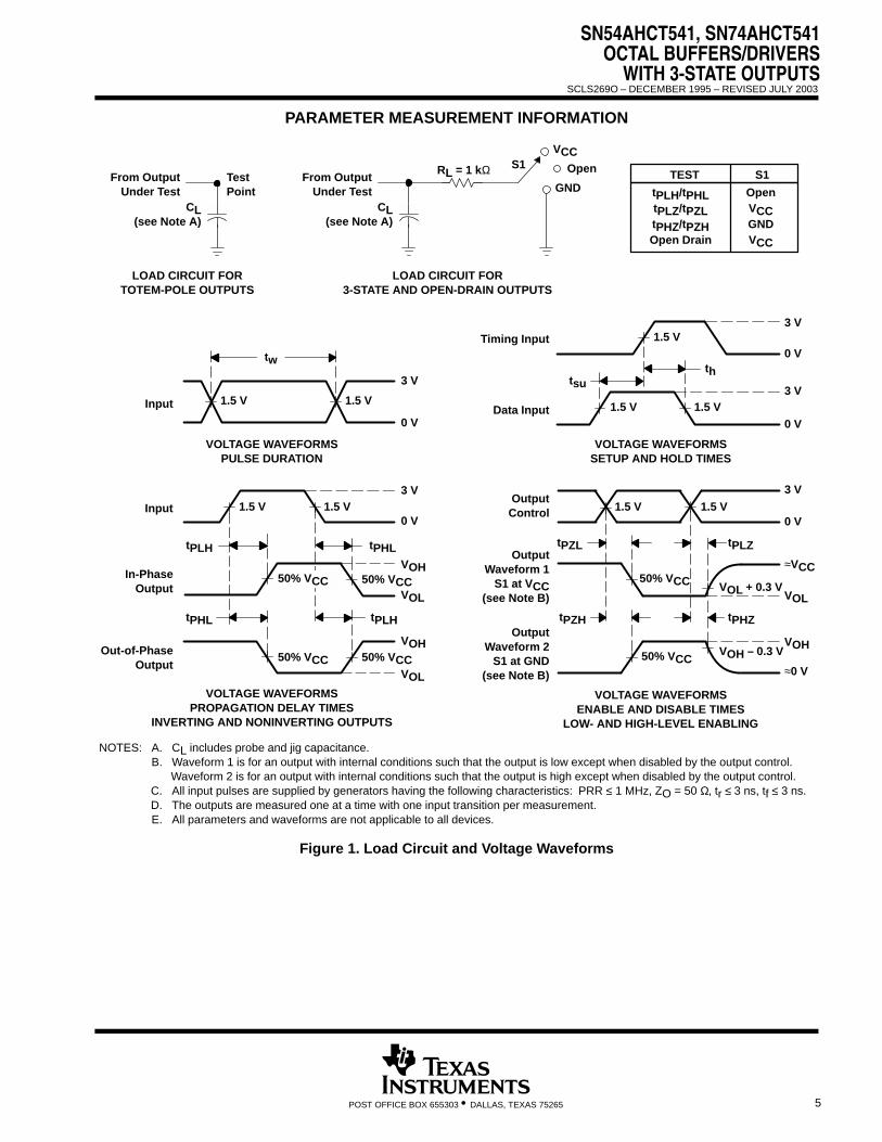
SN54AHCT541, SN74AHCT541OCTAL BUFFERS/DRIVERS
WITH 3-STATE OUTPUTS
SCLS269O – DECEMBER 1995 – REVISED JULY 2003
5POST OFFICE BOX 655303 • DALLAS, TEXAS 75265
PARAMETER MEASUREMENT INFORMATION
50% VCC
3 V
3 V
0 V
0 V
thtsu
VOLTAGE WAVEFORMSSETUP AND HOLD TIMES
Data Input
tPLH
tPHL
tPHL
tPLH
VOH
VOH
VOL
VOL
3 V
0 V
50% VCC50% VCC
Input
Out-of-PhaseOutput
In-PhaseOutput
Timing Input
50% VCC
VOLTAGE WAVEFORMSPROPAGATION DELAY TIMES
INVERTING AND NONINVERTING OUTPUTS
OutputControl
OutputWaveform 1
S1 at VCC(see Note B)
OutputWaveform 2
S1 at GND(see Note B)
VOL
VOH
tPZL
tPZH
tPLZ
tPHZ
≈VCC
0 V
50% VCC VOL + 0.3 V
50% VCC≈0 V
3 V
VOLTAGE WAVEFORMSENABLE AND DISABLE TIMES
LOW- AND HIGH-LEVEL ENABLING
tPLH/tPHLtPLZ/tPZLtPHZ/tPZHOpen Drain
OpenVCCGNDVCC
TEST S1
3 V
0 V
tw
VOLTAGE WAVEFORMSPULSE DURATION
Input
NOTES: A. CL includes probe and jig capacitance.B. Waveform 1 is for an output with internal conditions such that the output is low except when disabled by the output control.
Waveform 2 is for an output with internal conditions such that the output is high except when disabled by the output control.C. All input pulses are supplied by generators having the following characteristics: PRR ≤ 1 MHz, ZO = 50 Ω, tr ≤ 3 ns, tf ≤ 3 ns.D. The outputs are measured one at a time with one input transition per measurement.E. All parameters and waveforms are not applicable to all devices.
From OutputUnder Test
CL(see Note A)
LOAD CIRCUIT FOR3-STATE AND OPEN-DRAIN OUTPUTS
S1VCC
RL = 1 kΩGND
From OutputUnder Test
CL(see Note A)
TestPoint
LOAD CIRCUIT FORTOTEM-POLE OUTPUTS
Open
VOH – 0.3 V
1.5 V 1.5 V
1.5 V
1.5 V 1.5 V
1.5 V 1.5 V1.5 V 1.5 V
Figure 1. Load Circuit and Voltage Waveforms

MCFP006B − JANUARY 1995 − REVISED JULY 2003
1POST OFFICE BOX 655303 • DALLAS, TEXAS 75265
W (R-GDFP-F20) CERAMIC DUAL FLATPACK
10 11
0.250 (6,35)0.370 (9,40)
201
0.245 (6,22)
0.004 (0,10)
0.026 (0,66)
4 Places
0.015 (0,38)
0.045 (1,14)
0.009 (0,23)
0.045 (1,14)
Base and Seating Plane
0.005 (0,13) MIN
0.022 (0,56)
0.300 (7,62)
0.100 (2,54)
4040180-4/D 07/03
0.320 (8,13) MAX
0.250 (6,35)0.370 (9,40)
0.540 (13,72)MAX
0.050 (1,27)
NOTES: A. All linear dimensions are in inches (millimeters).B. This drawing is subject to change without notice.C. This package can be hermetically sealed with a ceramic lid using glass frit.D. Index point is provided on cap for terminal identification only.E. Falls within Mil-Std 1835 GDFP2-F20

MECHANICAL DATA
MLCC006B – OCTOBER 1996
1POST OFFICE BOX 655303 • DALLAS, TEXAS 75265
FK (S-CQCC-N**) LEADLESS CERAMIC CHIP CARRIER
4040140/D 10/96
28 TERMINAL SHOWN
B
0.358(9,09)
MAX
(11,63)
0.560(14,22)
0.560
0.458
0.858(21,8)
1.063(27,0)
(14,22)
ANO. OF
MINMAX
0.358
0.660
0.761
0.458
0.342(8,69)
MIN
(11,23)
(16,26)0.640
0.739
0.442
(9,09)
(11,63)
(16,76)
0.962
1.165
(23,83)0.938
(28,99)1.141
(24,43)
(29,59)
(19,32)(18,78)
**
20
28
52
44
68
84
0.020 (0,51)
TERMINALS
0.080 (2,03)0.064 (1,63)
(7,80)0.307
(10,31)0.406
(12,58)0.495
(12,58)0.495
(21,6)0.850
(26,6)1.047
0.045 (1,14)
0.045 (1,14)0.035 (0,89)
0.035 (0,89)
0.010 (0,25)
121314151618 17
11
10
8
9
7
5
432
0.020 (0,51)0.010 (0,25)
6
12826 27
19
21B SQ
A SQ22
23
24
25
20
0.055 (1,40)0.045 (1,14)
0.028 (0,71)0.022 (0,54)
0.050 (1,27)
NOTES: A. All linear dimensions are in inches (millimeters).B. This drawing is subject to change without notice.C. This package can be hermetically sealed with a metal lid.D. The terminals are gold plated.E. Falls within JEDEC MS-004

MPDI002C – JANUARY 1995 – REVISED DECEMBER 20002
1POST OFFICE BOX 655303 • DALLAS, TEXAS 75265
N (R-PDIP-T**) PLASTIC DUAL-IN-LINE PACKAGE
BB AC AD
0.325 (8,26)0.300 (7,62)
0.010 (0,25) NOM
Gauge Plane
0.015 (0,38)
0.430 (10,92) MAX
20
1.060(26,92)
0.940(23,88)
18
0.920
0.850
14
0.775
0.745
(19,69)
(18,92)
16
0.775(19,69)
(18,92)0.745
A MIN
DIM
A MAX
PINS **
(23,37)
(21,59)
Seating Plane
14/18 PIN ONLY20 pin vendor option
4040049/E 12/2002
9
80.070 (1,78)
A
0.045 (1,14)0.020 (0,51) MIN
16
1
0.015 (0,38)0.021 (0,53)
0.200 (5,08) MAX
0.125 (3,18) MIN
0.240 (6,10)0.260 (6,60)
M0.010 (0,25)
0.100 (2,54)
16 PINS SHOWN
MS-100VARIATION
AAC
D
D
D0.030 (0,76)
0.045 (1,14)
NOTES: A. All linear dimensions are in inches (millimeters).B. This drawing is subject to change without notice.
C. Falls within JEDEC MS-001, except 18 and 20 pin minimum body lrngth (Dim A).
D. The 20 pin end lead shoulder width is a vendor option, either half or full width.

MECHANICAL DATA
MSOI003E – JANUARY 1995 – REVISED SEPTEMBER 2001
1POST OFFICE BOX 655303 • DALLAS, TEXAS 75265
DW (R-PDSO-G**) PLASTIC SMALL-OUTLINE PACKAGE16 PINS SHOWN
0.419 (10,65)0.400 (10,15)
0.291 (7,39)0.299 (7,59)
16
0.400(10,16)
A MIN
A MAX(10,41)0.410 0.462
(11,73)
(11,51)0.453
18
0.610(15,49)
(15,24)0.600
24DIM
PINS **
4040000/E 08/01
0.104 (2,65) MAX 0.004 (0,10)0.012 (0,30)
Seating Plane
0°– 8°0.016 (0,40)0.050 (1,27)
16
0.050 (1,27)
1
A
8
90.014 (0,35)0.020 (0,51)
0.010 (0,25) NOM
Gage Plane
0.010 (0,25)
28
0.710(18,03)
0.700(17,78)(12,70)
(12,95)
0.500
20
0.510
0.010 (0,25)
0.004 (0,10)
NOTES: A. All linear dimensions are in inches (millimeters).B. This drawing is subject to change without notice.C. Body dimensions do not include mold flash or protrusion not to exceed 0.006 (0,15).D. Falls within JEDEC MS-013


MECHANICAL DATA
MSSO002E – JANUARY 1995 – REVISED DECEMBER 2001
1POST OFFICE BOX 655303 • DALLAS, TEXAS 75265
DB (R-PDSO-G**) PLASTIC SMALL-OUTLINE
4040065 /E 12/01
28 PINS SHOWN
Gage Plane
8,207,40
0,550,95
0,25
38
12,90
12,30
28
10,50
24
8,50
Seating Plane
9,907,90
30
10,50
9,90
0,38
5,605,00
15
0,22
14
A
28
1
2016
6,506,50
14
0,05 MIN
5,905,90
DIM
A MAX
A MIN
PINS **
2,00 MAX
6,90
7,50
0,65 M0,15
0°–8°
0,10
0,090,25
NOTES: A. All linear dimensions are in millimeters.B. This drawing is subject to change without notice.C. Body dimensions do not include mold flash or protrusion not to exceed 0,15.D. Falls within JEDEC MO-150

MECHANICAL DATA
MTSS001C – JANUARY 1995 – REVISED FEBRUARY 1999
1POST OFFICE BOX 655303 • DALLAS, TEXAS 75265
PW (R-PDSO-G**) PLASTIC SMALL-OUTLINE PACKAGE14 PINS SHOWN
0,65 M0,10
0,10
0,25
0,500,75
0,15 NOM
Gage Plane
28
9,80
9,60
24
7,90
7,70
2016
6,60
6,40
4040064/F 01/97
0,30
6,606,20
8
0,19
4,304,50
7
0,15
14
A
1
1,20 MAX
14
5,10
4,90
8
3,10
2,90
A MAX
A MIN
DIMPINS **
0,05
4,90
5,10
Seating Plane
0°–8°
NOTES: A. All linear dimensions are in millimeters.B. This drawing is subject to change without notice.C. Body dimensions do not include mold flash or protrusion not to exceed 0,15.D. Falls within JEDEC MO-153

IMPORTANT NOTICE
Texas Instruments Incorporated and its subsidiaries (TI) reserve the right to make corrections, modifications,enhancements, improvements, and other changes to its products and services at any time and to discontinueany product or service without notice. Customers should obtain the latest relevant information before placingorders and should verify that such information is current and complete. All products are sold subject to TI’s termsand conditions of sale supplied at the time of order acknowledgment.
TI warrants performance of its hardware products to the specifications applicable at the time of sale inaccordance with TI’s standard warranty. Testing and other quality control techniques are used to the extent TIdeems necessary to support this warranty. Except where mandated by government requirements, testing of allparameters of each product is not necessarily performed.
TI assumes no liability for applications assistance or customer product design. Customers are responsible fortheir products and applications using TI components. To minimize the risks associated with customer productsand applications, customers should provide adequate design and operating safeguards.
TI does not warrant or represent that any license, either express or implied, is granted under any TI patent right,copyright, mask work right, or other TI intellectual property right relating to any combination, machine, or processin which TI products or services are used. Information published by TI regarding third-party products or servicesdoes not constitute a license from TI to use such products or services or a warranty or endorsement thereof.Use of such information may require a license from a third party under the patents or other intellectual propertyof the third party, or a license from TI under the patents or other intellectual property of TI.
Reproduction of information in TI data books or data sheets is permissible only if reproduction is withoutalteration and is accompanied by all associated warranties, conditions, limitations, and notices. Reproductionof this information with alteration is an unfair and deceptive business practice. TI is not responsible or liable forsuch altered documentation.
Resale of TI products or services with statements different from or beyond the parameters stated by TI for thatproduct or service voids all express and any implied warranties for the associated TI product or service andis an unfair and deceptive business practice. TI is not responsible or liable for any such statements.
Following are URLs where you can obtain information on other Texas Instruments products and applicationsolutions:
Products Applications
Amplifiers amplifier.ti.com Audio www.ti.com/audio
Data Converters dataconverter.ti.com Automotive www.ti.com/automotive
DSP dsp.ti.com Broadband www.ti.com/broadband
Interface interface.ti.com Digital Control www.ti.com/digitalcontrol
Logic logic.ti.com Military www.ti.com/military
Power Mgmt power.ti.com Optical Networking www.ti.com/opticalnetwork
Microcontrollers microcontroller.ti.com Security www.ti.com/security
Telephony www.ti.com/telephony
Video & Imaging www.ti.com/video
Wireless www.ti.com/wireless
Mailing Address: Texas Instruments
Post Office Box 655303 Dallas, Texas 75265
Copyright 2003, Texas Instruments Incorporated
7. SN74HC21: Dual 4-Input Positive-AND Gates
Texas Instruments Dual 4-Input Positive-AND Gates
SN74HC21
F -82

SN54HC21, SN74HC21DUAL 4-INPUT POSITIVE-AND GATES
SCLS087E – DECEMBER 1982 – REVISED AUGUST 2003
1POST OFFICE BOX 655303 • DALLAS, TEXAS 75265
Wide Operating Voltage Range of 2 V to 6 V
Outputs Can Drive Up To 10 LSTTL Loads
Low Power Consumption, 20-µA Max ICC
Typical tpd = 11 ns
±4-mA Output Drive at 5 V
Low Input Current of 1 µA Max
1
2
3
4
5
6
7
14
13
12
11
10
9
8
1A1BNC1C1D1Y
GND
VCC2D2CNC2B2A2Y
SN54HC21 . . . J OR W PACKAGESN74HC21 . . . D, N, NS, OR PW PACKAGE
(TOP VIEW)
3 2 1 20 19
9 10 11 12 13
4
5
6
7
8
18
17
16
15
14
2CNCNCNC2B
NCNC1CNC1D
1B 1A NC
2Y 2AV 2D
1YG
ND
NC
SN54HC21 . . . FK PACKAGE(TOP VIEW)
CC
NC – No internal connection
description/ordering information
These devices contain two independent 4-input AND gates. They perform the Boolean function
Y A • B • C • D or Y A B C D in positive logic.
ORDERING INFORMATION
TA PACKAGE† ORDERABLEPART NUMBER
TOP-SIDEMARKING
–40 C to 85 C
PDIP – N Tube of 25 SN74HC21N SN74HC21N
–40 C to 85 C
SOIC – D
Tube of 50 SN74HC21D
HC21
–40 C to 85 C
SOIC – D Reel of 2500 SN74HC21DR HC21
–40°C to 85°CReel of 250 SN74HC21DT
–40°C to 85°CSOP – NS Reel of 2000 SN74HC21NSR HC21
TSSOP – PW
Tube of 90 SN74HC21PW
HC21TSSOP – PW Reel of 2000 SN74HC21PWR HC21
Reel of 250 SN74HC21PWT
–55 C to 125 C
CDIP – J Tube of 25 SNJ54HC21J SNJ54HC21J
–55°C to 125°C CFP – W Tube of 150 SNJ54HC21W SNJ54HC21W
LCCC – FK Tube of 55 SNJ54HC21FK SNJ54HC21FK† Package drawings, standard packing quantities, thermal data, symbolization, and PCB design guidelines are
available at www.ti.com/sc/package.
Please be aware that an important notice concerning availability, standard warranty, and use in critical applications ofTexas Instruments semiconductor products and disclaimers thereto appears at the end of this data sheet.
Copyright 2003, Texas Instruments IncorporatedPRODUCTION DATA information is current as of publication date.Products conform to specifications per the terms of Texas Instrumentsstandard warranty. Production processing does not necessarily includetesting of all parameters.
On products compliant to MIL-PRF-38535, all parameters are testedunless otherwise noted. On all other products, productionprocessing does not necessarily include testing of all parameters.
SN54HC21, SN74HC21DUAL 4-INPUT POSITIVE-AND GATES
SCLS087E – DECEMBER 1982 – REVISED AUGUST 2003
2 POST OFFICE BOX 655303 • DALLAS, TEXAS 75265
FUNCTION TABLE(each gate)
INPUTS OUTPUTA B C D
OUTPUTY
H H H H H
L X X X L
X L X X L
X X L X L
X X X L L
logic diagram (positive logic)
1A1Y1B
1C1D
2A2Y2B
2C2D
1245
9101213
6 8
Pin numbers shown are for the D, J, N, NS, PW, and W packages.
absolute maximum ratings over operating free-air temperature range (unless otherwise noted)†
Supply voltage range, VCC –0.5 V to 7 V. . . . . . . . . . . . . . . . . . . . . . . . . . . . . . . . . . . . . . . . . . . . . . . . . . . . . . . . . . Input clamp current, IIK (VI < 0 or VI > VCC) (see Note 1) ±20 mA. . . . . . . . . . . . . . . . . . . . . . . . . . . . . . . . . . . . Output clamp current, IOK (VO < 0 or VO > VCC) (see Note 1) ±20 mA. . . . . . . . . . . . . . . . . . . . . . . . . . . . . . . . Continuous output current, IO (VO = 0 to VCC) ±25 mA. . . . . . . . . . . . . . . . . . . . . . . . . . . . . . . . . . . . . . . . . . . . . . Continuous current through VCC or GND ±50 mA. . . . . . . . . . . . . . . . . . . . . . . . . . . . . . . . . . . . . . . . . . . . . . . . . . . Package thermal impedance, θJA (see Note 2): D package 86°C/W. . . . . . . . . . . . . . . . . . . . . . . . . . . . . . . . . . .
N package 80°C/W. . . . . . . . . . . . . . . . . . . . . . . . . . . . . . . . . . . NS package 76°C/W. . . . . . . . . . . . . . . . . . . . . . . . . . . . . . . . . PW package 113°C/W. . . . . . . . . . . . . . . . . . . . . . . . . . . . . . . .
Storage temperature range, Tstg –65°C to 150°C. . . . . . . . . . . . . . . . . . . . . . . . . . . . . . . . . . . . . . . . . . . . . . . . . . .
† Stresses beyond those listed under “absolute maximum ratings” may cause permanent damage to the device. These are stress ratings only, andfunctional operation of the device at these or any other conditions beyond those indicated under “recommended operating conditions” is notimplied. Exposure to absolute-maximum-rated conditions for extended periods may affect device reliability.
NOTES: 1. The input and output voltage ratings may be exceeded if the input and output current ratings are observed.2. The package thermal impedance is calculated in accordance with JESD 51-7.
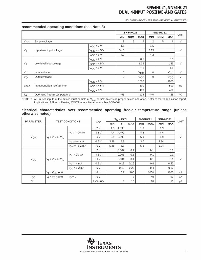
SN54HC21, SN74HC21DUAL 4-INPUT POSITIVE-AND GATES
SCLS087E – DECEMBER 1982 – REVISED AUGUST 2003
3POST OFFICE BOX 655303 • DALLAS, TEXAS 75265
recommended operating conditions (see Note 3)
SN54HC21 SN74HC21UNIT
MIN NOM MAX MIN NOM MAXUNIT
VCC Supply voltage 2 5 6 2 5 6 V
V High-level input voltage
VCC = 2 V 1.5 1.5
VVIH High-level input voltage VCC = 4.5 V 3.15 3.15 VIHVCC = 6 V 4.2 4.2
V Low-level input voltage
VCC = 2 V 0.5 0.5
VVIL Low-level input voltage VCC = 4.5 V 1.35 1.35 VILVCC = 6 V 1.8 1.8
VI Input voltage 0 VCC 0 VCC V
VO Output voltage 0 VCC 0 VCC V
t/ v Input transition rise/fall time
VCC = 2 V 1000 1000
ns∆t/∆v Input transition rise/fall time VCC = 4.5 V 500 500 ns
VCC = 6 V 400 400
TA Operating free-air temperature –55 125 –40 85 °C
NOTE 3: All unused inputs of the device must be held at VCC or GND to ensure proper device operation. Refer to the TI application report,Implications of Slow or Floating CMOS Inputs, literature number SCBA004.
electrical characteristics over recommended operating free-air temperature range (unlessotherwise noted)
PARAMETER TEST CONDITIONS VCCTA = 25°C SN54HC21 SN74HC21
UNITPARAMETER TEST CONDITIONS VCCMIN TYP MAX MIN MAX MIN MAX
UNIT
V V = V or V
I = –20 A
2 V 1.9 1.998 1.9 1.9
VV V = V or V
IOH = –20 µA 4.5 V 4.4 4.499 4.4 4.4
VVOH VI = VIH or VIL
OH6 V 5.9 5.999 5.9 5.9 VOH I IH IL
IOH = –4 mA 4.5 V 3.98 4.3 3.7 3.84
IOH = –5.2 mA 6 V 5.48 5.8 5.2 5.34
V V = V or V
I = 20 A
2 V 0.002 0.1 0.1 0.1
VV V = V or V
IOL = 20 µA 4.5 V 0.001 0.1 0.1 0.1
VVOL VI = VIH or VIL
OL6 V 0.001 0.1 0.1 0.1 VOL I IH IL
IOL = 4 mA 4.5 V 0.17 0.26 0.4 0.33
IOL = 5.2 mA 6 V 0.15 0.26 0.4 0.33
II VI = VCC or 0 6 V ±0.1 ±100 ±1000 ±1000 nA
ICC VI = VCC or 0, IO = 0 6 V 2 40 20 µA
Ci 2 V to 6 V 3 10 10 10 pF

SN54HC21, SN74HC21DUAL 4-INPUT POSITIVE-AND GATES
SCLS087E – DECEMBER 1982 – REVISED AUGUST 2003
4 POST OFFICE BOX 655303 • DALLAS, TEXAS 75265
switching characteristics over recommended operating free-air temperature range, CL = 50 pF(unless otherwise noted) (see Figure 1)
PARAMETERFROM TO
VCCTA = 25°C SN54HC21 SN74HC21
UNITPARAMETERFROM
(INPUT)TO
(OUTPUT)VCC
MIN TYP MAX MIN MAX MIN MAXUNIT
t A, B, C, or D Y
2 V 44 110 165 140
nstpd A, B, C, or D Y 4.5 V 14 22 33 28 nspd6 V 11 19 28 24
t Y
2 V 29 75 110 95
nstt Y 4.5 V 10 15 22 19 nst6 V 8 13 19 16
operating characteristics, TA = 25°CPARAMETER TEST CONDITIONS TYP UNIT
Cpd Power dissipation capacitance per gate No load 25 pF
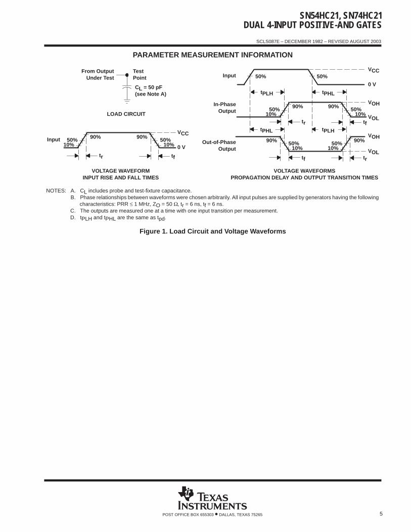
SN54HC21, SN74HC21DUAL 4-INPUT POSITIVE-AND GATES
SCLS087E – DECEMBER 1982 – REVISED AUGUST 2003
5POST OFFICE BOX 655303 • DALLAS, TEXAS 75265
PARAMETER MEASUREMENT INFORMATION
VOLTAGE WAVEFORMINPUT RISE AND FALL TIMES
50%50%10%10%
90% 90%VCC
0 V
tr tf
Input
VOLTAGE WAVEFORMSPROPAGATION DELAY AND OUTPUT TRANSITION TIMES
50%
50%50%10%10%
90% 90%
VCC
VOH
VOL
0 V
tr tf
Input
In-PhaseOutput
50%
tPLH tPHL
50% 50%10% 10%
90%90%VOH
VOLtrtf
tPHL tPLH
Out-of-PhaseOutput
TestPoint
From OutputUnder Test
CL = 50 pF(see Note A)
LOAD CIRCUIT
NOTES: A. CL includes probe and test-fixture capacitance.B. Phase relationships between waveforms were chosen arbitrarily. All input pulses are supplied by generators having the following
characteristics: PRR ≤ 1 MHz, ZO = 50 Ω, tr = 6 ns, tf = 6 ns.C. The outputs are measured one at a time with one input transition per measurement.D. tPLH and tPHL are the same as tpd.
Figure 1. Load Circuit and Voltage Waveforms


MECHANICAL DATA
MLCC006B – OCTOBER 1996
1POST OFFICE BOX 655303 • DALLAS, TEXAS 75265
FK (S-CQCC-N**) LEADLESS CERAMIC CHIP CARRIER
4040140/D 10/96
28 TERMINAL SHOWN
B
0.358(9,09)
MAX
(11,63)
0.560(14,22)
0.560
0.458
0.858(21,8)
1.063(27,0)
(14,22)
ANO. OF
MINMAX
0.358
0.660
0.761
0.458
0.342(8,69)
MIN
(11,23)
(16,26)0.640
0.739
0.442
(9,09)
(11,63)
(16,76)
0.962
1.165
(23,83)0.938
(28,99)1.141
(24,43)
(29,59)
(19,32)(18,78)
**
20
28
52
44
68
84
0.020 (0,51)
TERMINALS
0.080 (2,03)0.064 (1,63)
(7,80)0.307
(10,31)0.406
(12,58)0.495
(12,58)0.495
(21,6)0.850
(26,6)1.047
0.045 (1,14)
0.045 (1,14)0.035 (0,89)
0.035 (0,89)
0.010 (0,25)
121314151618 17
11
10
8
9
7
5
432
0.020 (0,51)0.010 (0,25)
6
12826 27
19
21B SQ
A SQ22
23
24
25
20
0.055 (1,40)0.045 (1,14)
0.028 (0,71)0.022 (0,54)
0.050 (1,27)
NOTES: A. All linear dimensions are in inches (millimeters).B. This drawing is subject to change without notice.C. This package can be hermetically sealed with a metal lid.D. The terminals are gold plated.E. Falls within JEDEC MS-004

MPDI002C – JANUARY 1995 – REVISED DECEMBER 20002
1POST OFFICE BOX 655303 • DALLAS, TEXAS 75265
N (R-PDIP-T**) PLASTIC DUAL-IN-LINE PACKAGE
BB AC AD
0.325 (8,26)0.300 (7,62)
0.010 (0,25) NOM
Gauge Plane
0.015 (0,38)
0.430 (10,92) MAX
20
1.060(26,92)
0.940(23,88)
18
0.920
0.850
14
0.775
0.745
(19,69)
(18,92)
16
0.775(19,69)
(18,92)0.745
A MIN
DIM
A MAX
PINS **
(23,37)
(21,59)
Seating Plane
14/18 PIN ONLY20 pin vendor option
4040049/E 12/2002
9
80.070 (1,78)
A
0.045 (1,14)0.020 (0,51) MIN
16
1
0.015 (0,38)0.021 (0,53)
0.200 (5,08) MAX
0.125 (3,18) MIN
0.240 (6,10)0.260 (6,60)
M0.010 (0,25)
0.100 (2,54)
16 PINS SHOWN
MS-100VARIATION
AAC
D
D
D0.030 (0,76)
0.045 (1,14)
NOTES: A. All linear dimensions are in inches (millimeters).B. This drawing is subject to change without notice.
C. Falls within JEDEC MS-001, except 18 and 20 pin minimum body lrngth (Dim A).
D. The 20 pin end lead shoulder width is a vendor option, either half or full width.
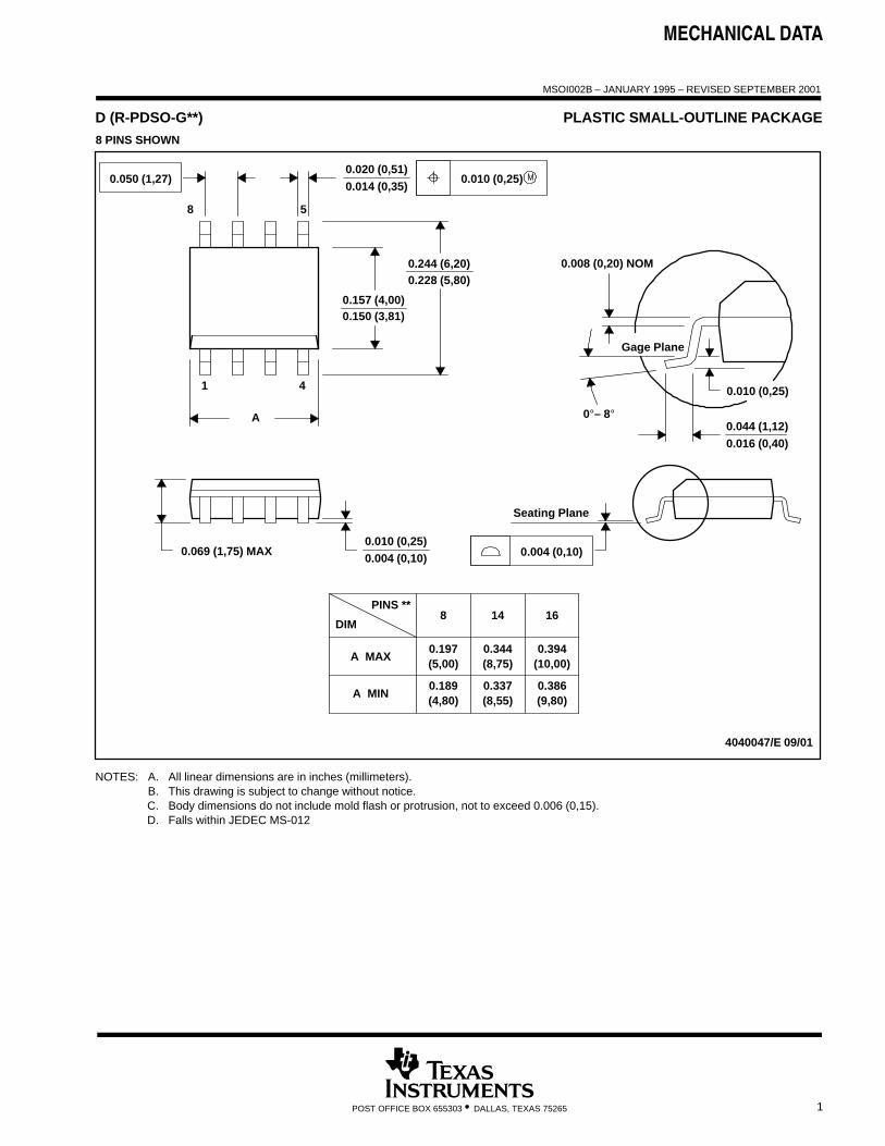
MECHANICAL DATA
MSOI002B – JANUARY 1995 – REVISED SEPTEMBER 2001
1POST OFFICE BOX 655303 • DALLAS, TEXAS 75265
D (R-PDSO-G**) PLASTIC SMALL-OUTLINE PACKAGE8 PINS SHOWN
8
0.197(5,00)
A MAX
A MIN(4,80)0.189 0.337
(8,55)
(8,75)0.344
14
0.386(9,80)
(10,00)0.394
16DIM
PINS **
4040047/E 09/01
0.069 (1,75) MAX
Seating Plane
0.004 (0,10)0.010 (0,25)
0.010 (0,25)
0.016 (0,40)0.044 (1,12)
0.244 (6,20)0.228 (5,80)
0.020 (0,51)0.014 (0,35)
1 4
8 5
0.150 (3,81)0.157 (4,00)
0.008 (0,20) NOM
0°– 8°
Gage Plane
A
0.004 (0,10)
0.010 (0,25)0.050 (1,27)
NOTES: A. All linear dimensions are in inches (millimeters).B. This drawing is subject to change without notice.C. Body dimensions do not include mold flash or protrusion, not to exceed 0.006 (0,15).D. Falls within JEDEC MS-012


MECHANICAL DATA
MTSS001C – JANUARY 1995 – REVISED FEBRUARY 1999
1POST OFFICE BOX 655303 • DALLAS, TEXAS 75265
PW (R-PDSO-G**) PLASTIC SMALL-OUTLINE PACKAGE14 PINS SHOWN
0,65 M0,10
0,10
0,25
0,500,75
0,15 NOM
Gage Plane
28
9,80
9,60
24
7,90
7,70
2016
6,60
6,40
4040064/F 01/97
0,30
6,606,20
8
0,19
4,304,50
7
0,15
14
A
1
1,20 MAX
14
5,10
4,90
8
3,10
2,90
A MAX
A MIN
DIMPINS **
0,05
4,90
5,10
Seating Plane
0°–8°
NOTES: A. All linear dimensions are in millimeters.B. This drawing is subject to change without notice.C. Body dimensions do not include mold flash or protrusion not to exceed 0,15.D. Falls within JEDEC MO-153

IMPORTANT NOTICE
Texas Instruments Incorporated and its subsidiaries (TI) reserve the right to make corrections, modifications,enhancements, improvements, and other changes to its products and services at any time and to discontinueany product or service without notice. Customers should obtain the latest relevant information before placingorders and should verify that such information is current and complete. All products are sold subject to TI’s termsand conditions of sale supplied at the time of order acknowledgment.
TI warrants performance of its hardware products to the specifications applicable at the time of sale inaccordance with TI’s standard warranty. Testing and other quality control techniques are used to the extent TIdeems necessary to support this warranty. Except where mandated by government requirements, testing of allparameters of each product is not necessarily performed.
TI assumes no liability for applications assistance or customer product design. Customers are responsible fortheir products and applications using TI components. To minimize the risks associated with customer productsand applications, customers should provide adequate design and operating safeguards.
TI does not warrant or represent that any license, either express or implied, is granted under any TI patent right,copyright, mask work right, or other TI intellectual property right relating to any combination, machine, or processin which TI products or services are used. Information published by TI regarding third-party products or servicesdoes not constitute a license from TI to use such products or services or a warranty or endorsement thereof.Use of such information may require a license from a third party under the patents or other intellectual propertyof the third party, or a license from TI under the patents or other intellectual property of TI.
Reproduction of information in TI data books or data sheets is permissible only if reproduction is withoutalteration and is accompanied by all associated warranties, conditions, limitations, and notices. Reproductionof this information with alteration is an unfair and deceptive business practice. TI is not responsible or liable forsuch altered documentation.
Resale of TI products or services with statements different from or beyond the parameters stated by TI for thatproduct or service voids all express and any implied warranties for the associated TI product or service andis an unfair and deceptive business practice. TI is not responsible or liable for any such statements.
Following are URLs where you can obtain information on other Texas Instruments products and applicationsolutions:
Products Applications
Amplifiers amplifier.ti.com Audio www.ti.com/audio
Data Converters dataconverter.ti.com Automotive www.ti.com/automotive
DSP dsp.ti.com Broadband www.ti.com/broadband
Interface interface.ti.com Digital Control www.ti.com/digitalcontrol
Logic logic.ti.com Military www.ti.com/military
Power Mgmt power.ti.com Optical Networking www.ti.com/opticalnetwork
Microcontrollers microcontroller.ti.com Security www.ti.com/security
Telephony www.ti.com/telephony
Video & Imaging www.ti.com/video
Wireless www.ti.com/wireless
Mailing Address: Texas Instruments
Post Office Box 655303 Dallas, Texas 75265
Copyright 2003, Texas Instruments Incorporated

8. 564-0700-111F: 3mm LED CBI Tri-Level Circuit Board Indicator
Dialight 3mm LED CBI Tri-Level Circuit Board Indicator
564-0700-111F
F -95
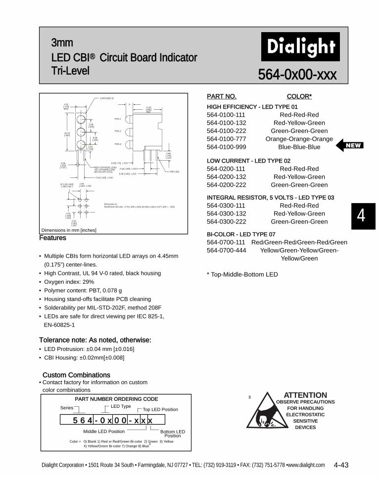
4-43Dialight Corporation • 1501 Route 34 South • Farmingdale, NJ 07727 • TEL: (732) 919-3119 • FAX: (732) 751-5778 •www.dialight.com
4
3mmLED CBI® Circuit Board IndicatorTri-Level 564-0x00-xxx
11.56[.455]REF
A
4.45[.175] ±.010
2.54 [.100] ±.010
2.54 [.100] ±.010
2.54[.100]
5.08[.200]
15.24[.600]
4.32[.170]MAX
3.68[.145]±.010
5.08[.200]
( TYP )
5.08 [.200] ±.010
CATHODE ID
RED CATHODE LEADYEL CATHODE LEAD(BI-COLOR LEDs)
POS.1
POS.2
POS.3
TOP LED
5.08[.200]
2.54[.100]±.002
2.54[.100] ±.002
Ø 1.09 [.043]±.002 ( 6X )
Dimension A:Red/Green Bi-color 2.76 [.109 ±.015] all other colors 2.67 [.103 +- .015]
2.54[.100]±.002
PART NO. COLOR*
HIGH EFFICIENCY - LED TYPE 01564-0100-111 Red-Red-Red564-0100-132 Red-Yellow-Green564-0100-222 Green-Green-Green564-0100-777 Orange-Orange-Orange564-0100-999 Blue-Blue-Blue
LOW CURRENT - LED TYPE 02564-0200-111 Red-Red-Red564-0200-132 Red-Yellow-Green564-0200-222 Green-Green-Green
INTEGRAL RESISTOR, 5 VOLTS - LED TYPE 03564-0300-111 Red-Red-Red564-0300-132 Red-Yellow-Green564-0300-222 Green-Green-Green
BI-COLOR - LED TYPE 07564-0700-111 Red/Green-Red/Green-Red/Green564-0700-444 Yellow/Green-Yellow/Green-
Yellow/Green
* Top-Middle-Bottom LED
Features
• Multiple CBIs form horizontal LED arrays on 4.45mm
(0.175”) center-lines.
• High Contrast, UL 94 V-0 rated, black housing
• Oxygen index: 29%
• Polymer content: PBT, 0.078 g
• Housing stand-offs facilitate PCB cleaning
• Solderability per MIL-STD-202F, method 208F
• LEDs are safe for direct viewing per IEC 825-1,
EN-60825-1
Tolerance note: As noted, otherwise:• LED Protrusion: ±0.04 mm [±0.016]
• CBI Housing: ±0.02mm[±0.008]
Custom Combinations• Contact factory for information on custom
color combinations
Dimensions in mm [inches]
5 6 4 - 0 x 0 0 - x x x
Top LED Position
Bottom LEDPosition
Middle LED Position
LED TypeSeries
PART NUMBER ORDERING CODE
Color = 0) Blank 1) Red or Red/Green Bi-color 2) Green 3) Yellow 4) Yellow/Green Bi-color 7) Orange 8) Blue³
NEW
ATTENTIONOBSERVE PRECAUTIONS
FOR HANDLINGELECTROSTATIC
SENSITIVEDEVICES
³

9. HEF4521B: 24-Stage Frequency Divider and Oscillator
Philips Semiconductor 24-Stage Frequency Divider and Oscillator
HEF4521B
F -97

!
"#$%
&#'()(*+,-'"*+,+,
&#'()(*+,-'.(/"+,+,
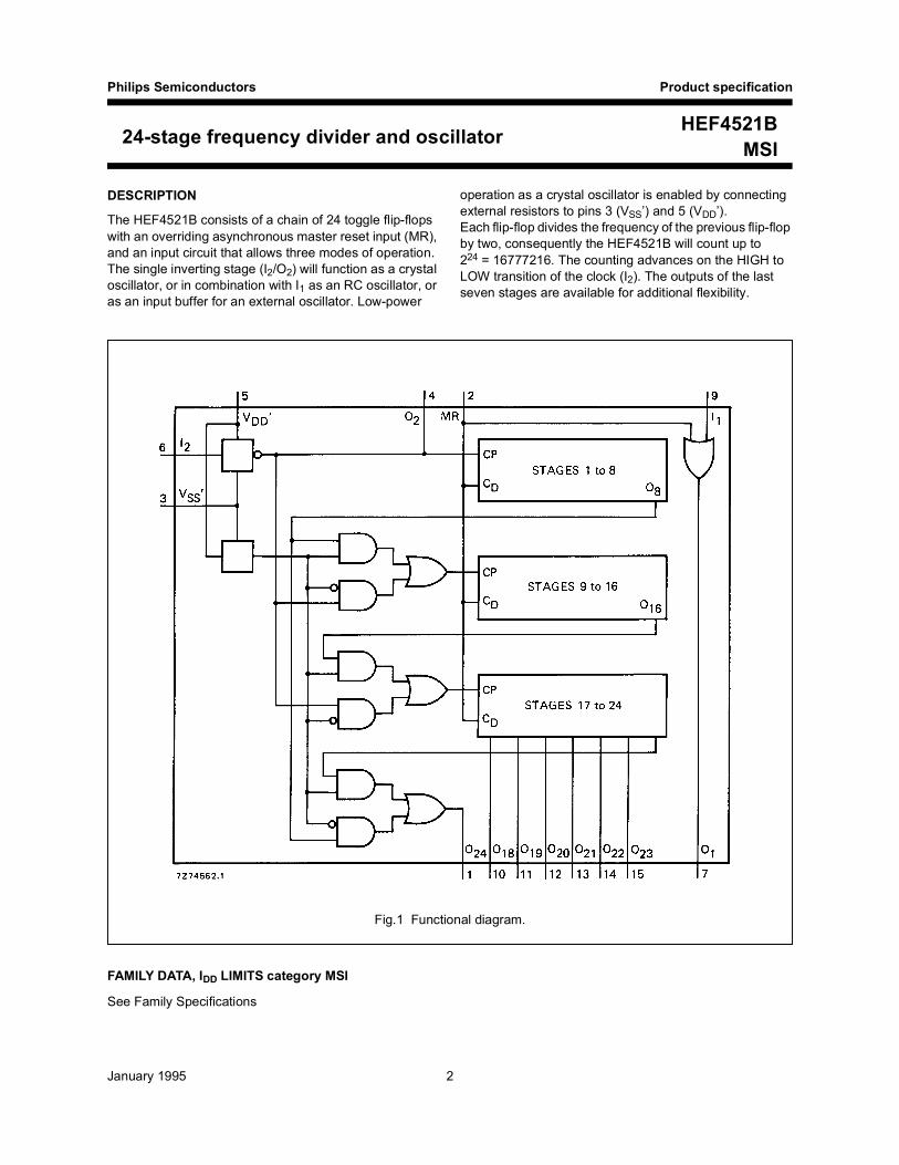
!"#
$%&'()
&#+,- #
$#!#"0)12
#$#"3
&#!0/(2$
"4$# 1
453'$$
44
5607**820799823
,#!# #!
4$ #+,-$
: ;<<<;3&#!#+=+
'(>#.023&##
!!4543
*+,$*'*- $$ +'"
*"*
3"3

6
#*"
!+,-
)*
+,-0?2% ;9'@ 0*(&6A2
+,-902% ;9'@ "02 0*(&<2
+,-&092% ;*(@ 0*(&2
0 2%.9?#B"
3"3
%(.)'%**%',
(.'.' %(.)'%**%',
(A A : ;
( : AA
( : A<;
( : <
( : 6
(6 6 : A6AA;A
( : ;<<<;
.)%'()*+''/.)%
).'%()'&(+
'&)*+(.'.'
&*&0
& ( 12 1$$2 (3 (
+ ' ' 799 7** ' #A
"@ (
0( $2@
4)1
' 799 7** + . (
0#!#'(>
+=+2
' ' ' 7** 7** + 7**8 7**
' + ' 7** 7** + # "+=+
' + ' 7** 799 + 7998 799@ (
$"C4"
@#!$#
"
' 7** 799 '"+=+
'(>
B#4##
" 53&#
!##A
47**8 799 7998 7**3 7
0(2 #
#A3B$
+=+3
&#$#"
47**8 7** 7998
7993 (" $##$
#"+=+
'(>3

#*"
!+,-
)*
#*"
!+,-
)*
*%%*&*%'&'%
7** : 7@&"4 : @ ' :@"
1$$
1 ,(+ )4 ',4 *54
',%*+
5'&*(+*'()
(&.+*
(A 6 0/2'
+=+'(> +' 6 < 66 06/2'
0;/2'
6 0/2'
'(>+=+ '+ 6 < 66 06/2'
0;/2'
( ( A 6 0/2'
+=+'(> +' 6 06/2'
0;/2'
A 6 0/2'
'(>+=+ '+ 6 06/2'
0;/2'
)1 ( 6 0/2'
+=+'(> +' 06/2'
A 6 0;/2'
( A ;6 0/2'
+=+'(> +' 6 < 06/2'
< 0;/2'
; 66 0/2'
'(>+=+ '+ 6 ; 06/2'
0;/2'
3*#"".3

;
#*"
!+,-
)*
*%%*&*%'&'%
7** : 7@&"4 : @ ' :@"
(" ; 0/2'
+=+'(> &+' 6 ; 0/2'
; 0A/2'
; 0/2'
'(>+=+ &'+ 6 ; 0/2'
; 0A/2'
1$$
1,(+ )4 ',4 *54
)"" A
$!"
3
$#@+=+ >+
6
)"")1 < 6
$#@+=+ >)1+
6
1!"
)1 1)1
)5"". ; )+D
"5 )+D
< 6 )+D
1$$
1',%*+(&.+*(& 678
9"$ 0'2 799 $#
0'2 799 : 30)+D2
.02 6 0'2 799 : 30)+D2
' : 02
0'2 : "
799 : !072
1$$
1 ,(+ )4 ',4 *54
',%*+
5'&*(+*'()
(&.+*
<
#*"
!+,-
)*
3>!"#$"""$#)1 !")13

A
#*"
!+,-
)*
*+%*'())(&*'()
2%
99 :;
%&%.'
9 :;
%&%.'.)'
#
.+D
* ?
!@1* ; .
,5/!
1 < < .
& A A
*
3;3
02 ($$3
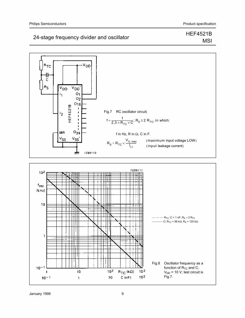
#*"
!+,-
)*
3< 1@
+D1 3
6 1& @ 1* 1& $##%
1* 1&
7' "5
'
"5"" ! '(>
.
3A (
1& @
799 : 7@
3<3
1&@ : @1* 1&
@ 1& : ;.@1* : .
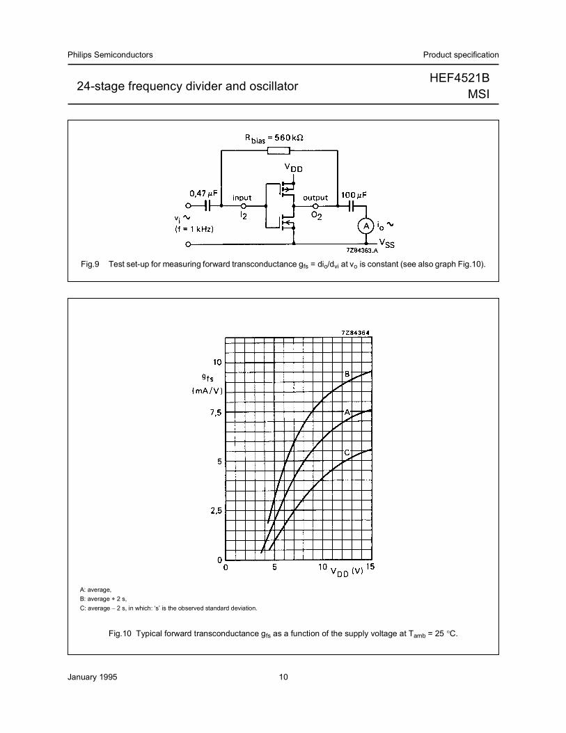
#*"
!+,-
)*
3 &"$ : /! ! 0#323
3&$ #!&"4 : 3
B%!
-%!E
%! $##%F8#4!!3
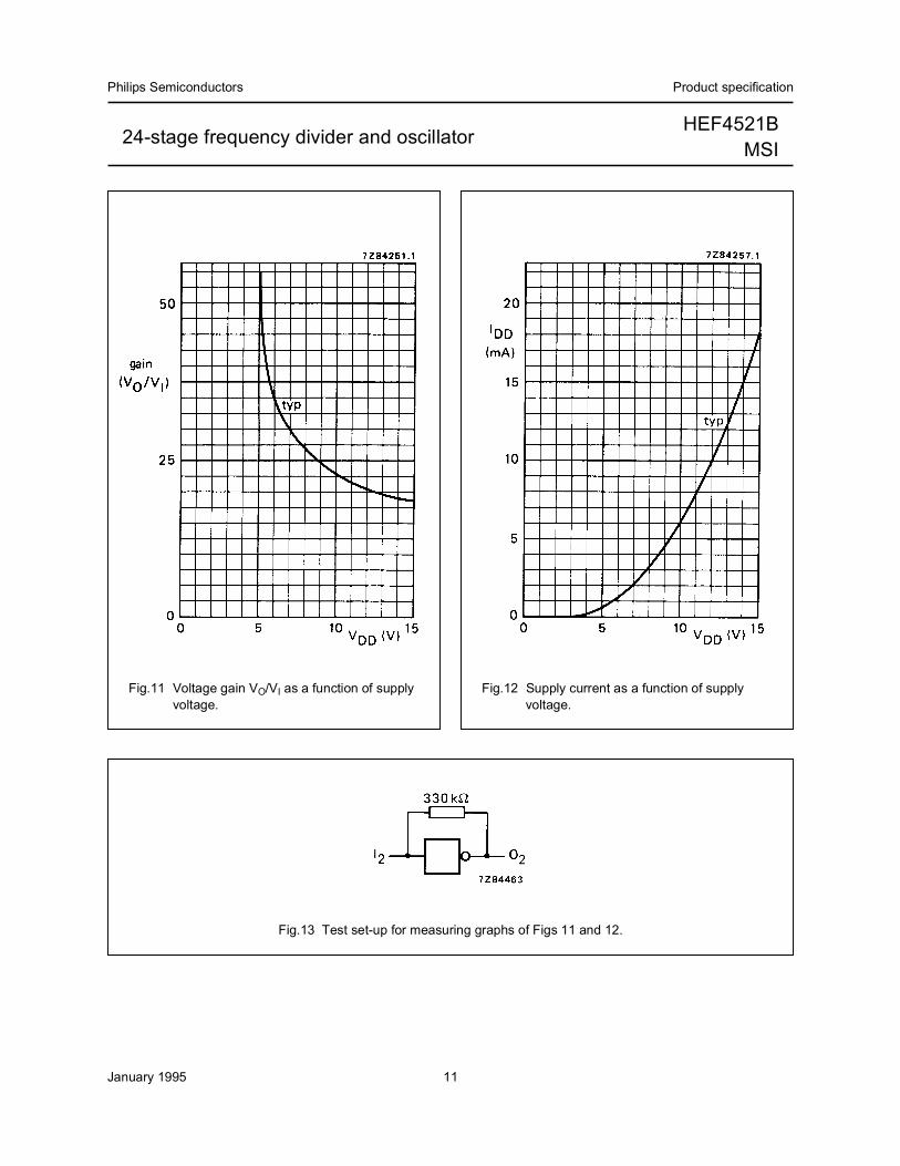
#*"
!+,-
)*
3 77(/7
!3
3 *
!3
36&"#3

10. 179-009-513R571: Center Dual Port D-SUB Female/Female
NorComp Center Dual Port D-SUB
Female/Female 179-009-513R571
F -109


11. LTC1441/SO: Ultra Low Power Dual Comparator with Reference
Linear Technology Ultra Low Power Dual Comparator
with Reference LTC1441/SO
F -111

1
LTC1440/LTC1441/LTC1442
144012fd
APPLICATIO SU
Ultralow Power Single/DualComparator with Reference
V +R11.65M1%
R21.13M1%
3.3V
V –
2 1
7
8
GND
OUT
LTC1440
1440 TA01
IN+
IN–
HYST
REF
3
4
5
6
–
+
TEMPERATURE (°C) –40
5.0
4.5
4.0
3.5
3.0
2.5
2.0
1.520 60
1440/1/2 TA02
–20 0 40 80 100
SUPP
LY C
URRE
NT (µ
A)
V+ = 5VV– = GND = 0V
Micropower 2.9V VCC Threshold DetectorLTC1440 Supply Current vs Temperature
The LTC®1440/LTC1441/LTC1442 are ultralow powersingle and dual comparators with built-in references. Thecomparators feature less than 3.7µA supply current overtemperature (LTC1440), a 1.182V ±1% reference, pro-grammable hysteresis (LTC1440/LTC1442) and TTL/CMOSoutputs that sink and source current. The reference outputcan drive a bypass capacitor of up to 0.01µF withoutoscillation.
The comparators operate from a single 2V to 11V supplyor a dual ±1V to ±5.5V supply (LTC1440). Comparatorhysteresis is easily programmed by using two resistorsand the HYST pin (LTC1440/LTC1442). Each comparator’sinput operates from the negative supply to within 1.3V ofthe positive supply. The comparator output stage cancontinuously source up to 40mA. By eliminating thecross-conducting current that normally happens when thecomparator changes logic states, the power supply glitchesare eliminated.
The LTC1440 is available in 8-pin PDIP, SO, MSOP andDFN packages. The LTC1441/LTC1442 are available in8-pin PDIP and SO packages.
Battery-Powered System Monitoring Threshold Detectors Window Comparators Oscillator Circuits
Ultralow Quiescent Current: 2.1µA Typ (LTC1440) Reference Output Drives 0.01µF Capacitor Adjustable Hysteresis (LTC1440/LTC1442) Wide Supply Range:
Single: 2V to 11VDual: ±1V to ±5.5V
Input Voltage Range Includes the Negative Supply TTL/CMOS Compatible Outputs 12µs Propagation Delay with 10mV Overdrive No Crowbar Current 40mA Continuous Source Current Pin Compatible Upgrades for MAX921/922/923 3mm x 3mm x 0.75mm DFN Package (LTC1440)
FEATURES DESCRIPTIO
U
TYPICAL APPLICATIO
U
, LT, LTC and LTM are registered trademarks of Linear Technology Corporation.All other trademarks are the property of their respective owners.

2
LTC1440/LTC1441/LTC1442
144012fd
S8 PARTMARKING
VoltageV + to V –, V + to GND, GND to V – ...........12V to –0.3VIN +, IN –, HYST ................. (V + + 0.3V) to (V – – 0.3V)REF ................................... (V + + 0.3V) to (V – – 0.3V)OUT (LTC1440) .............. (V + + 0.3V) to (GND – 0.3V)OUT (LTC1441/LTC1442) ... (V + + 0.3V) to (V – – 0.3V)
CurrentIN +, IN –, HYST ................................................. 20mAREF ................................................................... 20mAOUT .................................................................. 50mA
ABSOLUTE MAXIMUM RATINGS
W WW U
OUT Short-Circuit Duration (V + ≤ 5.5V) .......ContinuousPower Dissipation .............................................. 500mWOperating Temperature Range
LTC144XC ............................................... 0°C to 70°CLTC144XI ........................................... –40°C to 85°C
Storage Temperature Range ................. –65°C to 150°CStorage Temperature Range
(DD Package) ................................... –65°C to 125°CJunction Temperature ........................................... 150°CJunction Temperature (DD Package) .................... 125°CLead Temperature (Soldering, 10 sec).................. 300°C
PACKAGE/ORDER INFORMATION
W UU
Consult LTC Marketing for parts specified with wider operating temperature ranges.* The temperature grade is identified by a label on the shipping container.
(Note 1)
TJMAX = 150°C, θJA = 130°C/ W (N8)TJMAX = 150°C, θJA = 175°C/ W (S8)
TJMAX = 150°C, θJA = 250°C/ W
ORDER PARTNUMBER
LTC1440CDDLTC1440IDD
DD8 PARTMARKING*
LBTH
ORDER PARTNUMBER
LTC1440CMS8LTC1440IMS8
MS8 PARTMARKING*
LTBX
ORDER PARTNUMBER
LTC1440CN8LTC1440CS8LTC1440IN8LTC1440IS8
S8 PARTMARKING
144014401440I1440I
TJMAX = 125°C, θJA = 160°C/ W (DD)UNDERSIDE METAL CONNECTED TO V–
(PCB CONNECTION OPTIONAL)
1
2
3
4
8
7
6
5
TOP VIEW
GND
V–
IN+
IN–
OUT
V+
REF
HYST
S8 PACKAGE8-LEAD PLASTIC SO
N8 PACKAGE8-LEAD PDIP
ORDER PARTNUMBER
ORDER PARTNUMBER
S8 PARTMARKING
14411441I
TJMAX = 150°C, θJA = 130°C/ W (N8)TJMAX = 150°C, θJA = 175°C/ W (S8)
TJMAX = 150°C, θJA = 130°C/ W (N8)TJMAX = 150°C, θJA = 175°C/ W (S8)
1
2
3
4
8
7
6
5
TOP VIEW
OUT A
V–
IN A+
IN A–
OUT B
V+
IN B+
IN B–
S8 PACKAGE8-LEAD PLASTIC SO
N8 PACKAGE8-LEAD PDIP
1
2
3
4
8
7
6
5
TOP VIEW
OUT A
V–
IN A+
IN B–
OUT B
V+
REF
HYST
S8 PACKAGE8-LEAD PLASTIC SO
N8 PACKAGE8-LEAD PDIP
LTC1441CN8LTC1441CS8LTC1441IN8LTC1441IS8
LTC1442CN8LTC1442CS8LTC1442IN8LTC1442IS8
14421442I
1234
GNDV–
IN+
IN–
8765
OUTV+
REFHYST
TOP VIEW
MS8 PACKAGE8-LEAD PLASTIC MSOP
TOP VIEW
DD PACKAGE8-LEAD (3mm × 3mm) PLASTIC DFN
5
6
7
8
4
3
2
1GND
V–
IN+
IN–
OUT
V+
REF
HYST
Order Options Tape and Reel: Add #TRLead Free: Add #PBF Lead Free Tape and Reel: Add #TRPBF Lead Free Part Marking: http://www.linear.com/leadfree/
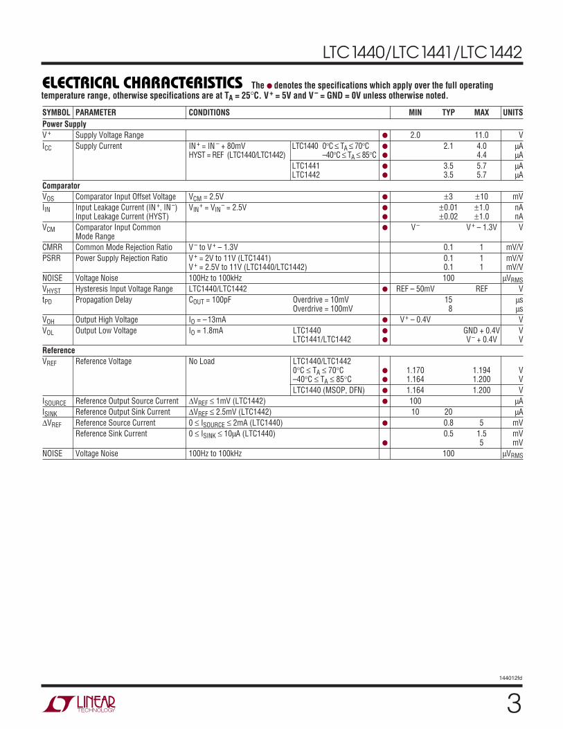
3
LTC1440/LTC1441/LTC1442
144012fd
ELECTRICAL CHARACTERISTICS The denotes the specifications which apply over the full operatingtemperature range, otherwise specifications are at TA = 25°C. V + = 5V and V – = GND = 0V unless otherwise noted.
SYMBOL PARAMETER CONDITIONS MIN TYP MAX UNITSPower SupplyV + Supply Voltage Range 2.0 11.0 VICC Supply Current IN + = IN – + 80mV LTC1440 0°C ≤ TA ≤ 70°C 2.1 4.0 µA
HYST = REF (LTC1440/LTC1442) –40°C ≤ TA ≤ 85°C 4.4 µALTC1441 3.5 5.7 µALTC1442 3.5 5.7 µA
ComparatorVOS Comparator Input Offset Voltage VCM = 2.5V ±3 ±10 mVIIN Input Leakage Current (IN +, IN –) VIN
+ = VIN– = 2.5V ±0.01 ±1.0 nA
Input Leakage Current (HYST) ±0.02 ±1.0 nAVCM Comparator Input Common V – V + – 1.3V V
Mode RangeCMRR Common Mode Rejection Ratio V – to V + – 1.3V 0.1 1 mV/VPSRR Power Supply Rejection Ratio V + = 2V to 11V (LTC1441) 0.1 1 mV/V
V + = 2.5V to 11V (LTC1440/LTC1442) 0.1 1 mV/VNOISE Voltage Noise 100Hz to 100kHz 100 µVRMSVHYST Hysteresis Input Voltage Range LTC1440/LTC1442 REF – 50mV REF VtPD Propagation Delay COUT = 100pF Overdrive = 10mV 15 µs
Overdrive = 100mV 8 µsVOH Output High Voltage IO = –13mA V + – 0.4V VVOL Output Low Voltage IO = 1.8mA LTC1440 GND + 0.4V V
LTC1441/LTC1442 V – + 0.4V VReferenceVREF Reference Voltage No Load LTC1440/LTC1442
0°C ≤ TA ≤ 70°C 1.170 1.194 V–40°C ≤ TA ≤ 85°C 1.164 1.200 VLTC1440 (MSOP, DFN) 1.164 1.200 V
ISOURCE Reference Output Source Current ∆VREF ≤ 1mV (LTC1442) 100 µAISINK Reference Output Sink Current ∆VREF ≤ 2.5mV (LTC1442) 10 20 µA∆VREF Reference Source Current 0 ≤ ISOURCE ≤ 2mA (LTC1440) 0.8 5 mV
Reference Sink Current 0 ≤ ISINK ≤ 10µA (LTC1440) 0.5 1.5 mV 5 mV
NOISE Voltage Noise 100Hz to 100kHz 100 µVRMS

4
LTC1440/LTC1441/LTC1442
144012fd
ELECTRICAL CHARACTERISTICS The denotes the specifications which apply over the full operatingtemperature range, otherwise specifications are at TA = 25°C. V + = 3V and V – = GND = 0V unless otherwise noted.
Note 1: Stresses beyond those listed under Absolute Maximum Ratingsmay cause permanent damage to the device. Exposure to any AbsoluteMaximum Rating condition for extended periods may affect devicereliability and lifetime.
SYMBOL PARAMETER CONDITIONS MIN TYP MAX UNITSPower SupplyV + Supply Voltage Range 2 11 V
ICC Supply Current IN + = IN – + 80mV LTC1440 0°C ≤ TA ≤ 70°C 2 3.9 µAHYST = REF (LTC1440/LTC1442) –40°C ≤ TA ≤ 85°C 4.3 µA
LTC1441 3.5 5.7 µALTC1442 3.5 5.7 µA
ComparatorVOS Comparator Input Offset Voltage VCM = 1.5V ±3 ±10 mVIIN Input Leakage Current (IN +, IN –) VIN
+ = VIN– = 1.5V ±0.01 ±1 nA
Input Leakage Current (HYST) ±0.02 ±1 nAVCM Comparator Input Common V – V + – 1.3V V
Mode RangeCMRR Common Mode Rejection Ratio V – to V + – 1.3V 0.1 1 mV/VPSRR Power Supply Rejection Ratio V + = 2V to 11V (LTC1441) 0.1 1 mV/V
V + = 2.5V to 11V (LTC1440/LTC1442) 0.1 1 mV/VNOISE Voltage Noise 100Hz to 100kHz 100 µVRMSVHYST Hysteresis Input Voltage Range LTC1440/LTC1442 REF – 50mV REF VtPD Propagation Delay COUT = 100pF Overdrive = 10mV 14 µs
Overdrive = 100mV 5 µsVOH Output High Voltage IO = –8mA V + – 0.4V VComparatorVOL Output Low Voltage IO = 0.8mA LTC1440 GND + 0.4V V
LTC1441/LTC1442 V – + 0.4V VReferenceVREF Reference Voltage No Load LTC1440/LTC1442
0°C ≤ TA ≤ 70°C 1.170 1.182 1.194 V–40°C ≤ TA ≤ 85°C 1.164 1.200 VLTC1440 (MSOP, DFN) 1.164 1.200 V
ISOURCE Reference Output Source Current ∆VREF ≤ 1mV (LTC1442) 60 120 µAISINK Reference Output Sink Current ∆VREF ≤ 2.5mV (LTC1442) 10 20 µA∆VREF Reference Source Current 0 ≤ ISOURCE ≤ 1mA (LTC1440) 0.8 5.5 mV
Reference Sink Current 0 ≤ ISINK ≤ 10µA (LTC1440) 0.5 1.5 mV 5 mV
NOISE Voltage Noise 100Hz to 100kHz 100 µVRMS

5
LTC1440/LTC1441/LTC1442
144012fd
RESPONSE TIME (µs)–1
INPU
T VO
LTAG
E (m
V)OU
TPUT
VOL
TAGE
(V)
0
0
1
6 14 18
5
1440/1/2 G02
100
2 104 12 160 8
2
3
4100mV
10mV
50mV20mV
TA = 25°C
RESPONSE TIME (µs)–1
INPU
T VO
LTAG
E (m
V)OU
TPUT
VOL
TAGE
(V)
100
0
1
64
5
1440/1/2 G01
0
20 108
2
3
4 100mV 10mV
50mV 20mV
TA = 25°C
SUPPLY VOLTAGE (V)0
SOUR
CE C
URRE
NT (m
A)
3 5
1440/1/2 G04
1 2 4
160
140
120
100
80
60
40
20
0
OUT CONNECTED TOV– = GND = 0V
TYPICAL PERFOR A CE CHARACTERISTICS
UW
Comparator Response Time vsInput Overdrive
Comparator Short-Circuit SinkCurrent vs Supply Voltage
SUPPLY VOLTAGE (V)0
SINK
CUR
RENT
(mA)
200
180
160
140
120
100
80
60
40
20
08
1440/1/2 G03
21 3 5 7 94 6 10
OUT CONNECTED TO V+
TA = 25°C
Comparator Short-Circuit SourceCurrent vs Supply Voltage
Comparator Response Time vsInput Overdrive

6
LTC1440/LTC1441/LTC1442
144012fd
TYPICAL PERFOR A CE CHARACTERISTICS
UW
Comparator Response Time vsLoad Capacitance with 100mVInput Overdrive
Comparator Response Time atLow Supply Voltage
Comparator Output Voltage Highvs Load Current
LOAD CAPACITANCE (nF)0
RESP
ONSE
TIM
E (µ
s)
12
10
8
6
4
280
1440/1/2 G05
20 40 60 100
tPHL
tPLH
SUPPLY VOLTAGE (V)1.0
RESP
ONSE
TIM
E (µ
s)
10000
1000
100
10
11.2 1.4 1.61.1 1.3 1.5
1440/1/2 G06
20mV OVERDRIVE
100mV OVERDRIVE
LOAD CURRENT (mA)0
1
OUTP
UT V
OLTA
GE H
IGH
(V)
2
3
4
5
10 20 30 40
1440/1/2 G07
50 60
V+ = 5V
V+ = 3V
V+ = 2V
TA = 25°C
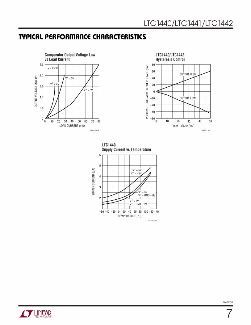
7
LTC1440/LTC1441/LTC1442
144012fd
TYPICAL PERFOR A CE CHARACTERISTICS
UW
Comparator Output Voltage Lowvs Load Current
LTC1440/LTC1442Hysteresis Control
VREF – VHYST (mV)0
POSI
TIVE
-TO-
NEGA
TIVE
INPU
T VO
LTAG
E (m
V)
30 50
1440/1/2 G09
10 20 40
80
60
40
20
0
–20
–40
–60
–80
OUTPUT HIGH
OUTPUT LOW
TEMPERATURE (°C)–60
SUPP
LY C
URRE
NT (µ
A)
6
5
4
3
2
1100
1440/1/2 G10
–20–40 20 40 80 1200 60 140
V+ = 5VV– = –5V
V+ = 5VV– = GND = 0V
V+ = 3VV– = GND = 0V
LTC1440Supply Current vs Temperature
LOAD CURRENT (mA)0
OUTP
UT V
OLTA
GE L
OW (V
)
1.5
2.0
2.5
30 50 80
1440/1/2 G08
1.0
0.5
010 20 40 60 70
V+ = 2V
V+ = 3V
V+ = 5V
TA = 25°C
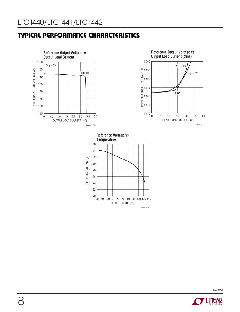
8
LTC1440/LTC1441/LTC1442
144012fd
OUTPUT LOAD CURRENT (mA)0
1.190
1.185
1.180
1.175
1.170
1.165
1.160
1.1551.5 2.5
1440/1/2 G11
0.5 1.0 2.0 3.0 3.5
REFE
RENC
E OU
TPUT
VOL
TAGE
(V)
VCC = 5V
SOURCE
Reference Output Voltage vsOutput Load Current
Reference Voltage vsTemperature
TEMPERATURE (°C)–60
REFE
RENC
E VO
LTAG
E (V
)
1.186
1.184
1.182
1.180
1.178
1.176
1.174
1.172
1.170100
1440/1/2 G13
–20–40 20 40 80 1200 60 140
OUTPUT LOAD CURRENT (µA)0
REFE
RENC
E OU
TPUT
VOL
TAGE
(V)
1.200
1.195
1.190
1.185
1.180
1.175
1.1705 10 15 20
1440/1/2 G12
25 30
VCC = 5V
SINK
VCC = 2V
Reference Output Voltage vsOutput Load Current (Sink)
TYPICAL PERFOR A CE CHARACTERISTICS
UW

9
LTC1440/LTC1441/LTC1442
144012fd
PIN FUNCTIONS
UUU
V – V +
OUT A LTC14411
2
3
4
8
7
6
5
IN A+
IN A–
IN B+
IN B–
OUT B
1440/1/2 PD
–+A
– +B
V –
V –
V +
OUT A LTC14421
2
3
4
8
7
6
5
IN A+
IN B–
REF
HYST
OUT B1
2
3
4
8
7
6
5
IN+
IN–HYST
REF
V+
OUT
–
+
V –
GNDLTC1440
–+ – +
A B
LTC1440GND (Pin 1): Ground. Connect to V – for single supplyoperation.
V – (Pin 2): Negative Supply. Connect to ground for singlesupply operation. Potential should be more negative thanGND.
IN + (Pin 3): Noninverting Comparator Input. Input com-mon mode range from V – to V + –1.3V. Input currenttypically 10pA at 25°C.
IN – (Pin 4): Inverting Comparator Input. Input commonmode range from V – to V + –1.3V. Input current typically10pA at 25°C.
HYST (Pin 5): Hysteresis Input. Connect to REF if notused. Input voltage range is from VREF to VREF – 50mV.
REF (Pin 6): Reference Output. 1.182V with respectto V –. Can source up to 200µA and sink 15µA at 25°C.Drive 0.01µF bypass capacitor without oscillation.
V + (Pin 7): Positive Supply. 2V to 11V.
OUT (Pin 8): Comparator CMOS Output. Swings fromGND to V +. Output can source up to 40mA and sink 5mA.
LTC1441OUT A (Pin 1): Comparator A CMOS Output. Swings fromV – to V +. Output can source up to 40mA and sink 5mA.
V – (Pin 2): Negative Supply.
IN A+ (Pin 3): Noninverting Input of Comparator A. Inputcommon mode range from V – to V + –1.3V. Input currenttypically 10pA at 25°C.
IN A– (Pin 4): Inverting Input of Comparator A. Inputcommon mode range from V – to V + –1.3V. Input currenttypically 10pA at 25°C.
IN B – (Pin 5): Inverting Input of Comparator B. Inputcommon mode range from V – to V + –1.3V. Input currenttypically 10pA at 25°C.
IN B + (Pin 6): Noninverting Input of Comparator B. Inputcommon mode range from V – to V + –1.3V. Input currenttypically 10pA at 25°C.
V + (Pin 7): Positive Supply. 2V to 11V.
OUT B (Pin 8): Comparator B CMOS Output. Swings fromV – to V +. Output can source up to 40mA and sink 5mA.
LTC1442OUT A (Pin 1): Comparator A CMOS Output. Swings fromV – to V +. Output can source up to 40mA and sink 5mA.
V – (Pin 2): Negative Supply.
IN A+ (Pin 3): Noninverting Input of Comparator A. Inputcommon mode range from V – to V + –1.3V. Input currenttypically 10pA at 25°C.
IN B– (Pin 4): Inverting Input of Comparator B. Inputcommon mode range from V – to V + –1.3V. Input currenttypically 10pA at 25°C.
HYST (Pin 5): Hysteresis Input. Connect to REF if notused. Input voltage range is from VREF to VREF – 50mV.
REF (Pin 6): Reference Output. 1.182V with respectto V –. Can source up to 200µA and sink 15µA at 25°C.Drive 0.01µF bypass capacitor without oscillation.
V + (Pin 7): Positive Supply. 2V to 11V.
OUT B (Pin 8): Comparator B CMOS Output. Swings fromV – to V +. Output can source up to 40mA and sink 5mA.

10
LTC1440/LTC1441/LTC1442
144012fd
LTC1440/LTC1441/LTC1442 are a family of micropowercomparators with built-in 1.182V reference. Featuresinclude programmable hysteresis (LTC1440/LTC1442),wide supply voltage range (2V to 11V) and the ability of thereference to drive up to a 0.01µF capacitor without oscil-lation. The comparators’ CMOS outputs can source up to40mA and the supply current glitches, that normally occurwhen switching logic states, have been eliminated.
Power Supplies
The comparator family operates from a single 2V to 11Vsupply. The LTC1440 includes a separate ground for thecomparator output stage, allowing a split supply rangingfrom ±1V to ±5.5V. Connecting V – to GND on the LTC1440will allow single supply operation. If the comparator out-put is required to source more than 1mA, or the supplysource impedance is high, V + should be bypassed with a0.1µF capacitor.
Comparator Inputs
The comparator inputs can swing from the negative sup-ply V – to within 1.3V max of the positive supply V +. Theinputs can be forced 300mV below V – or above V + withoutdamage and the typical input leakage current is only±10pA.
Comparator Outputs
The LTC1440 comparator output swings between GNDand V + to assure TTL compatibility with a split supply. TheLTC1441 and LTC1442 outputs swing between V – and V +.The outputs are capable of sourcing up to 40mA andsinking up to 5mA while still maintaining microamperequiescent currents. The output stage does not generatecrowbar switching currents during transitions which helpsminimize parasitic feedback through the supply pins.
Voltage Reference
The internal bandgap reference has a voltage of 1.182Vreferenced to V –. The reference accuracy is 1.5% from–40°C to 85°C. It can source up to 200µA and sink up to20µA with a 5V supply. The reference can drive a bypass
capacitor of up to 0.01µF without oscillation and byinserting a series resistor, capacitance values up to 100µFcan be used (Figure 1).
Figure 2 shows the resistor value required for differentcapacitor values to achieve critical damping. Bypassingthe reference can help prevent false tripping of the com-parators by preventing glitches on V + or reference loadtransients from disturbing the reference output voltage.
Figure 3 shows the bypassed reference output with asquare wave applied to the V + pin. Resistors R2 and R3 set10mV of hysteresis voltage band while R1 damps thereference response. Note that the comparator outputdoesn’t trip.
APPLICATIONS INFORMATION
WU UU
LTC144X
V –
REFR1
C1
REFERENCEOUTPUT
1440/1/2 F01
Figure 1. Damping the Reference Output
CAPACITOR VALUE (µF)0.001
0.1
RESI
STOR
VAL
UE (k
Ω)
10
1000
0.01 0.1 101
1440/1/2 F02
1
100
Figure 2. Damping Resistance vs Bypass Capacitor Value

11
LTC1440/LTC1441/LTC1442
144012fd
APPLICATIONS INFORMATION
WU UU
V +
R1430Ω
R210k
C11µF
5VTO8V
OUT
V –
2 1
7
8
GND
LTC1440
1440/1/2 F03a
IN+
IN–
HYST
REF
3
4
5
6
R32.4M
–
+
Figure 3a. Reference Transient Response Test Circuit
2ms/DIV 1440/1/2 F03b
8V V +
5V
VREF
OUT
Hysteresis
Hysteresis can be added to the LTC1440 by connecting aresistor (R1) between the REF and HYST pins and asecond resistor (R2) from HYST to V – (Figure 4).
The difference between the upper and lower thresholdvoltages, or hysteresis voltage band (VHB), is equal to twicethe voltage difference between the REF and HYST pins.
When more hysteresis is added, the upper thresholdincreases the same amount as the low threshold de-creases. The maximum voltage allowed between REF andHYST pins is 50mV, producing a maximum hysteresisvoltage band of 100mV. The hysteresis band could vary by
2mV/
DIV
up to 15%. If hysteresis is not wanted, the HYST pinshould be shorted to REF. Acceptable values for IREF rangefrom 0.1µA to 5µA. If 2.4M is chosen for R2, then the valueof R1 is equal to the value of VHB.
Figure 5. Glitch-Free Level Detector with Hysteresis
V +
R5430Ω5%
R315k1%
C11µF
OUT
V –
2 1
7
5VVIN
8
GND
LTC1440
1440/1/2 F05
IN+
IN–
HYST
REF
3
4
5
6
–
+
R23.4M1%
R11.18M1%
R42.4M1%
6
R2
HYSTV–
REF
5R1
1440/1/2 F04
LTC1440
2
IREFR1 =
VHB(2)(IREF)
R2 = IREF
1.182V –( )VHB2
Figure 4. Programmable Hysteresis
Level Detector
The LTC1440 is ideal for use as a micropower leveldetector as shown in Figure 5. R1 and R2 form a voltagedivider from VIN to the noninverting comparator input. R3and R4 set the hysteresis voltage, and R5 and C1 bypassthe reference output. The following design procedure canbe used to select the component values:
1. Choose the VIN voltage trip level, in this example 4.65V.
Figure 3b. Reference and Comparator OutputTransient Response

12
LTC1440/LTC1441/LTC1442
144012fd
APPLICATIONS INFORMATION
WU UU
2. Calculate the required resistive divider ratio.
Ratio = VREF/ VIN
Ratio = 1.182V/4.65V = 0.254
3. Choose the required hysteresis voltage band at theinput VHBIN, in this example 60mV. Calculate the hyster-esis voltage band referred to the comparator input VHB.
VHB = (VHBIN)(Ratio)
VHB = (60mV)(0.254)
VHB = 15.24mV
4. Choose the values for R3 and R4 to set the hysteresis.
R4 = 2.4M
R3(kΩ) = VHB = 15k
5. Choose the values for R1 and R2 to set the trip point.
RVI
VA
M
R RV
V V
REF
BIAS
IN
REFHB
11 182
11 18
2 1
2
1
= = =
=+
−
⎡
⎣
⎢⎢⎢⎢
⎤
⎦
⎥⎥⎥⎥
. .µ
R MV
V mV
R M
2 1 184 65
1 182 152
1
2 3 40
=+
−
⎡
⎣
⎢⎢⎢⎢
⎤
⎦
⎥⎥⎥⎥
=
. .
.
.
Low Voltage Operation
It is important to note that the voltage references internalto the LTC1440 and LTC1442 can exceed the commonmode range of the comparators at low supply voltages.The input common mode range of the LTC1440/LTC1441/LTC1442 comparators is guaranteed to extend up to (V+ -1.3V). Therefore, if one of the comparator inputs is at the1.182V reference voltage, the minimum supply voltage is2.5V for a valid output reading.
The guaranteed minimum operating voltage for theLTC1440/LTC1441/LTC1442 is 2V (or ±1V). However,both the reference and comparator(s) will function with asupply voltage as low as 1.5V, but performance willdegrade as the voltage goes below 2V. The voltage refer-ence temperature coefficient will degrade slightly, and thecomparators will have less output drive with an increase inpropagation delay. At the reduced supply voltages, theinput common mode range of the comparator(s) will stilltypically extend from the negative supply to approximately1.1V below the positive supply.

13
LTC1440/LTC1441/LTC1442
144012fd
10-Bit 30µA A/D Converter
–
+
5V
5V
2N3809
1N914
32.768kHz
VN2222LL
10pF100k
EIN0V TO 3V
365k*
470k
1M
10M150k
0.033µFPOLYSTYRENE
C11/2 LTC1441
LT®10341.2V
Q
D CLK74C74
CONVCOMMAND
DATAOUT
STATUS
1440/1/2 TA03
Q
1.2M
–
+C2
1/2 LTC1441
74C00
74C00 74C0074C00
*TRW-IRC MRT–5/+120ppm/°C
TYPICAL APPLICATIONS
U
32.768kHz “Watch Crystal” Oscillator
+V
32.768kHz
10pF
470k
1M
OUT
1440/1/2 TA05
1.2M
–
+1/2
LTC1441
14
LTC1440/LTC1441/LTC1442
144012fd
3.00 ±0.10(4 SIDES)
NOTE:1. DRAWING TO BE MADE A JEDEC PACKAGE OUTLINE M0-229 VARIATION OF (WEED-1)2. DRAWING NOT TO SCALE3. ALL DIMENSIONS ARE IN MILLIMETERS4. DIMENSIONS OF EXPOSED PAD ON BOTTOM OF PACKAGE DO NOT INCLUDE MOLD FLASH. MOLD FLASH, IF PRESENT, SHALL NOT EXCEED 0.15mm ON ANY SIDE5. EXPOSED PAD SHALL BE SOLDER PLATED6. SHADED AREA IS ONLY A REFERENCE FOR PIN 1 LOCATION
ON TOP AND BOTTOM OF PACKAGE
0.38 ± 0.10
BOTTOM VIEW—EXPOSED PAD
1.65 ± 0.10(2 SIDES)
0.75 ±0.05
R = 0.115TYP
2.38 ±0.10(2 SIDES)
14
85
PIN 1TOP MARK
(NOTE 6)
0.200 REF
0.00 – 0.05
(DD8) DFN 1203
0.25 ± 0.05
2.38 ±0.05(2 SIDES)
RECOMMENDED SOLDER PAD PITCH AND DIMENSIONS
1.65 ±0.05(2 SIDES)2.15 ±0.05
0.50BSC
0.675 ±0.05
3.5 ±0.05
PACKAGEOUTLINE
0.25 ± 0.050.50 BSC
MSOP (MS8) 0204
0.53 ± 0.152(.021 ± .006)
SEATINGPLANE
NOTE:1. DIMENSIONS IN MILLIMETER/(INCH)2. DRAWING NOT TO SCALE3. DIMENSION DOES NOT INCLUDE MOLD FLASH, PROTRUSIONS OR GATE BURRS. MOLD FLASH, PROTRUSIONS OR GATE BURRS SHALL NOT EXCEED 0.152mm (.006") PER SIDE4. DIMENSION DOES NOT INCLUDE INTERLEAD FLASH OR PROTRUSIONS. INTERLEAD FLASH OR PROTRUSIONS SHALL NOT EXCEED 0.152mm (.006") PER SIDE5. LEAD COPLANARITY (BOTTOM OF LEADS AFTER FORMING) SHALL BE 0.102mm (.004") MAX
0.18(.007)
0.254(.010)
1.10(.043)MAX
0.22 – 0.38(.009 – .015)
TYP
0.127 ± 0.076(.005 ± .003)
0.86(.034)REF
0.65(.0256)
BSC
0° – 6° TYP
DETAIL “A”
DETAIL “A”
GAUGE PLANE
1 2 3 4
4.90 ± 0.152(.193 ± .006)
8 7 6 5
3.00 ± 0.102(.118 ± .004)
(NOTE 3)
3.00 ± 0.102(.118 ± .004)
(NOTE 4)
0.52(.0205)
REF
5.23(.206)MIN
3.20 – 3.45(.126 – .136)
0.889 ± 0.127(.035 ± .005)
RECOMMENDED SOLDER PAD LAYOUT
0.42 ± 0.038(.0165 ± .0015)
TYP
0.65(.0256)
BSC
DD Package8-Lead Plastic DFN (3mm × 3mm)
(Reference LTC DWG # 05-08-1698)
MS8 Package8-Lead Plastic MSOP
(Reference LTC DWG # 05-08-1660)
U
PACKAGE DESCRIPTIO

15
LTC1440/LTC1441/LTC1442
144012fd
Information furnished by Linear Technology Corporation is believed to be accurate and reliable.However, no responsibility is assumed for its use. Linear Technology Corporation makes no represen-tation that the interconnection of its circuits as described herein will not infringe on existing patent rights.
PACKAGE DESCRIPTION
U
N8 Package8-Lead PDIP (Narrow 0.300)
(LTC DWG # 05-08-1510)
S8 Package8-Lead Plastic Small Outline (Narrow 0.150)
(LTC DWG # 05-08-1610)
N8 1002
.065(1.651)
TYP
.045 – .065(1.143 – 1.651)
.130 ± .005(3.302 ± 0.127)
.020(0.508)
MIN.018 ± .003(0.457 ± 0.076)
.120(3.048)
MIN
1 2 3 4
8 7 6 5
.255 ± .015*(6.477 ± 0.381)
.400*(10.160)
MAX
.008 – .015(0.203 – 0.381)
.300 – .325(7.620 – 8.255)
.325+.035–.015+0.889–0.3818.255( )
NOTE:1. DIMENSIONS ARE
INCHESMILLIMETERS
*THESE DIMENSIONS DO NOT INCLUDE MOLD FLASH OR PROTRUSIONS. MOLD FLASH OR PROTRUSIONS SHALL NOT EXCEED .010 INCH (0.254mm)
.100(2.54)BSC
.016 – .050(0.406 – 1.270)
.010 – .020(0.254 – 0.508)
× 45°
0°– 8° TYP.008 – .010
(0.203 – 0.254)
SO8 0303
.053 – .069(1.346 – 1.752)
.014 – .019(0.355 – 0.483)
TYP
.004 – .010(0.101 – 0.254)
.050(1.270)
BSC
1 2 3 4
.150 – .157(3.810 – 3.988)
NOTE 3
8 7 6 5
.189 – .197(4.801 – 5.004)
NOTE 3
.228 – .244(5.791 – 6.197)
.245MIN .160 ±.005
RECOMMENDED SOLDER PAD LAYOUT
.045 ±.005 .050 BSC
.030 ±.005 TYP
INCHES(MILLIMETERS)
NOTE:1. DIMENSIONS IN
2. DRAWING NOT TO SCALE3. THESE DIMENSIONS DO NOT INCLUDE MOLD FLASH OR PROTRUSIONS. MOLD FLASH OR PROTRUSIONS SHALL NOT EXCEED .006" (0.15mm)
16
LTC1440/LTC1441/LTC1442
144012fd
Linear Technology Corporation1630 McCarthy Blvd., Milpitas, CA 95035-7417(408) 432-1900 FAX: (408) 434-0507 www.linear.com
LT 0806 REV D • PRINTED IN USA
© LINEAR TECHNOLOGY CORPORATION 1996
10kHz V/F Converter
TYPICAL APPLICATION
U
RELATED PARTSPART NUMBER DESCRIPTION COMMENTS
LTC1443 1.182V Reference with Micropower Quad Comparators 1% Accuracy, 8.5µA Maximum Current, Ref Output Drives 0.01µF
LTC1444/LTC1445 1.2V Reference with Quad Comparator 1% Accuracy, 8.5µA Maximum Current, Ref Output Drives 0.01µFwith Adjustable Hysteresis
LTC1540 1.182V Reference with Nanopower Comparator DFN Package 0.3µA Quiescent Current (Typical), Referencewith Adjustable Hysteresis Drives 0.01µF
LTC1541 1.2V Reference with Micropower Amplifier and Comparator DFN Package 1.25% Accuracy, Rail-to-Rail Out, Low Offset Amplifier
LTC1842/LTC1843 1.82V Reference with Dual Comparators 1% Accuracy, Open-Drain Out, Reference Drives 0.01µFwith Adjustable Hysteresis
LTC1998 1.2 Reference with Comparator with Adjustable Thesholds Li-Ion Low Battery Monitor, SOT23, 1% Accuracy
LT6700-1 0.4 Reference with Low Voltage Dual Comparators SOT23, 1.4V to 18.5V Supply Range, ±2% Over TemperatureLT6700-2/LT6700-3
–
+
100pF**
50pF
2.2µF
1.2M*
10kHz TRIM200k
10M
100k
2k*
LM334
+V6.2V TO 12V
LT1034-1.2
LT1034-1.2
2.7M
C11/2 LTC1441
fOUT0kHz TO 10kHz
74C14
1440/1/2 TA04
0.01µF
0.1µF
INPUT0V TO 5V
Q5
Q6
15k
2M TYP100Hz TRIM
–
+
C21/2 LTC1441
Q1 Q8
Q2
Q3
Q4
0.47µF
Q7
= HP5082-2810
= 1N4148
= 2N2222
= 1% METAL FILM
= POLYSTYRENE*
**
+
+

12. 5227161-2: BNC Jack, Right Angle
Tyco Electronics BNC Jack, Right Angle
5227161-2
F -128

13. PJ-102BH: DC Power Jack
CUI Inc DC Power Jack PJ-102BH
F -130

3.0 0.12
10.7 0.42
0.194.7
3.0 0.12
4.7 0.19
3.0 0.12 3.0 0.12
6.50
9.0
0.26
6.50
11.0
2.50 0.10 0.26
0.430.35
3.5 0.14(TYP)
HOUSINGTERMINAL 3TERMINAL 2TERMINAL 1
X.XXX ±0.05mm
A
MATERIAL
CENTER PIN
TOLERANCE:X.X ±0.2mmX.XX ±0.1mm
PLATING
PJ-102BH
DC POWER JACK
COPYRIGHT 2006 BY CUI INC.
TITLE:
MM [INCHES]SCALE:
PJ-102BHPC FILE NAME: APPROVED BY:DRAWN BY:
UNITS:PART NO.
ZRJ 2:1
REV:
RoHS
Fax: 503-372-1266
9615 SW Allen Blvd., Ste. 103Beaverton, OR 97005Phone: 503-643-4899
800-275-4899
Website: www.cui.com
3
Silver
1
1
3
2
Brass
INSULATION RESISTANCE: 50M OHMS MIN: 100V DCCONTACT RESISTANCE: 50m OHMS MAX
LIFE: 5,000 CYCLESVOLTAGE WITHSTAND: 500V AC R.M.S. FOR 1 MINUTE
(3 PLCS)
TOP VIEW
CENTER PIN DIAMETER 2.5mm Dia.
PBT
Copper AlloyBrass
Copper
SilverSilverNickel
SPECIFICATIONS:RATING: 24V DC @ 5A
1.00X1.60
PCB LAYOUT
2
REV. DESCRIPTION DATEA NEW DRAWING 11/17/2005
PJ-102BH
SCHEMATIC
MODEL NO.
32
1
14.4 0.57
0.143.50
10.7 0.42
1.0 0.04(3 PLCS)