step by step - vysoké učení technické v brně · step by step cadance manual and examples...
TRANSCRIPT

Faculty of Electrical Engineering and Communication Department of Microelectronics
STEP BY STEP
CADANCE MANUAL AND EXAMPLES
Schematic
Ing. Ahmad Khateb, Ph.D.
Faculty of Electrical Engineering and Communication Department of Microelectronics
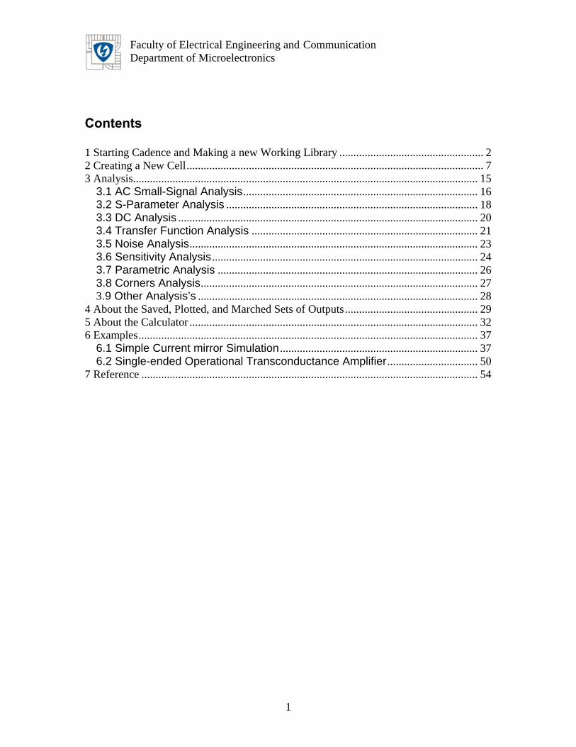
Contents 1 Starting Cadence and Making a new Working Library ................................................... 2 2 Creating a New Cell......................................................................................................... 7 3 Analysis.......................................................................................................................... 15
3.1 AC Small-Signal Analysis................................................................................... 16 3.2 S-Parameter Analysis ......................................................................................... 18 3.3 DC Analysis .......................................................................................................... 20 3.4 Transfer Function Analysis ................................................................................ 21 3.5 Noise Analysis...................................................................................................... 23 3.6 Sensitivity Analysis .............................................................................................. 24 3.7 Parametric Analysis ............................................................................................ 26 3.8 Corners Analysis.................................................................................................. 27 3.9 Other Analysis’s ................................................................................................... 28
4 About the Saved, Plotted, and Marched Sets of Outputs............................................... 29 5 About the Calculator ...................................................................................................... 32 6 Examples........................................................................................................................ 37
6.1 Simple Current mirror Simulation ...................................................................... 37 6.2 Single-ended Operational Transconductance Amplifier................................ 50
7 Reference ....................................................................................................................... 54
1

Faculty of Electrical Engineering and Communication Department of Microelectronics
Virtuoso® schematic composer
The Virtuoso® schematic composer is a design entry tool that supports the work of logic and circuit design engineers. Physical layout designers and printed circuit board designers can use the information as background material to support their work.
1 Starting Cadence and Making a new Working Library In order to organize your new circuits, you need to start the Common Desktop Environment and create a new library using the Cadence library manager to hold your design files. Carry out the following steps: 1. Enter your user name
2. Enter your password
3. Common Desktop Environment will appear
1. Click on the terminal icon 2. Write amiArtist then click Enter 3. Select your project number then click Enter 4. Select the version number then click Enter
2

Faculty of Electrical Engineering and Communication Department of Microelectronics
1- Click on the Terminal icon
2- Write amiArtist
3- Select your project number
4- Select the version number
4. Click Enter then you should get a window (called the Command Information Window - CIW). The CIW is the control window for the Cadence software. The following figure shows the parts of the CIW.
Window title Menu banner
Output area
Input line Mouse bindings line Prompt line
3

Faculty of Electrical Engineering and Communication Department of Microelectronics
• Window title displays the Cadence executable name and the path to the log file that records your current editing session. The log file appears in your home directory.
• Menu banner lets you display command menus to access all the Cadence design framework II tools.
• Output area displays a running history of the commands you execute and their results. For example, it displays a status message when you open a library. The area enlarges when you enlarge the CIW vertically.
• Input line is where you type in Cadence SKILL language expressions or type numeric values for commands instead of clicking on points.
• Mouse bindings line displays the current mouse button settings. These settings change as you move the mouse in and out of windows and start and stop commands.
• Prompt line reminds you of the next step during a command. Recommendation: Keep the Command Information Window - CIW in sight, from the CIW, you can access all Cadence tolls and functionalities
• view prompts, • view error and informational messages, • start specific tools, • run SKILL command
5. Library Manager will automatically be opened. If not, in the CIW, select Tools → Library Manager... You should get the following window, with the following list of libraries.
4
Faculty of Electrical Engineering and Communication Department of Microelectronics
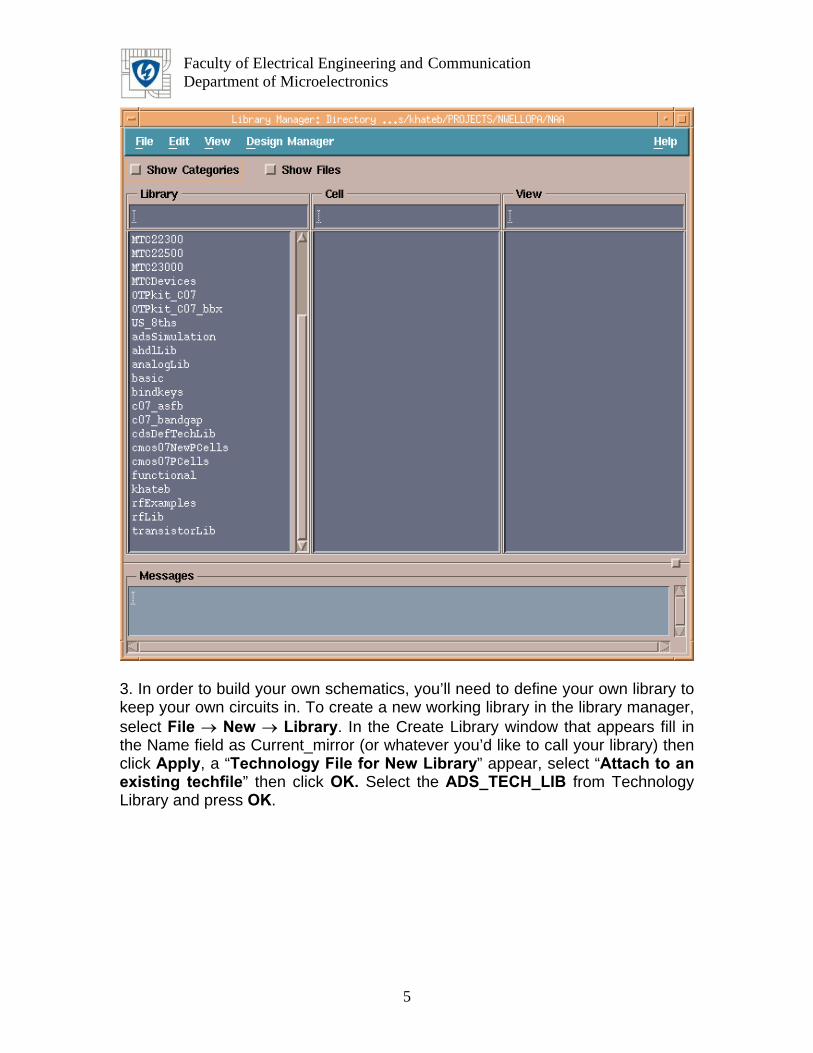
3. In order to build your own schematics, you’ll need to define your own library to keep your own circuits in. To create a new working library in the library manager, select File → New → Library. In the Create Library window that appears fill in the Name field as Current_mirror (or whatever you’d like to call your library) then click Apply, a “Technology File for New Library” appear, select “Attach to an existing techfile” then click OK. Select the ADS_TECH_LIB from Technology Library and press OK.
5

Faculty of Electrical Engineering and Communication Department of Microelectronics
6

Faculty of Electrical Engineering and Communication Department of Microelectronics
Now the working library has been created. All the project cells (components) that you generate should end up in this library. When you start up the Library Manager to begin working on your circuits, make sure you select your own library to work in.
2 Creating a New Cell When you create a new cell (component in the library), you actually create a view of the cell. For now we’ll be creating “schematic” views, but eventually you’ll have other different views of the same cell. For example a “layout” view of the same cell will have the composite layout information in it. It’s a different file, but it should represent the same circuit. This will be discussed later in more details. For now, we’re creating a schematic view. To create a cell view, carry out the following steps: 2.1 Creating the Schematic View of an Current_mirror
1. Select File → New → Cell View... from the Library Manager menu or to the CIW menu. The Create New File window appears. The Library Name field is Current_mirror. Fill in the Cell Name field as Current_mirror. Choose Composer-Schematic from the Tool list and the view name is automatically filled as Schematic. The library path file is automatically set. Click OK.
7

Faculty of Electrical Engineering and Communication Department of Microelectronics
2. A blank window called Virtuoso Schematic Editing: Current_mirror
Current_mirror Schematic appears.
Zoom In By 2
Zoom Out By 2
Stretch
Copy
Delete
Undo
Property
Save
Check & Save
narrow)
epeat R
Cmd Options
Pin
Wire Name
Wire (wide)
Wire (
Instance
3. Adding Instances: An instance (either a gate from the standard cell library
or a cell that you’ve designed earlier) can be placed in the schematic by selecting Add → Instance... or by pressing “i”, and the following Add Instance window appears.
8

Faculty of Electrical Engineering and Communication Department of Microelectronics
4. For this example, we need to add the following components: two identical
NMOS transistors of W/L= 20/3 um and one resistor of 15K ohm. To add the NMOS transistors, press Browse then select the transistorLib Library → M_NMOS Cell → symbol View, This opens the Add Instance window
9

Faculty of Electrical Engineering and Communication Department of Microelectronics
Now, enter the M_NMOS transistor value of W/L= 20/3 um and hit Hide. Place the first M_NMOS in the schematic window then press ”G” key from the keyboard for “Horizontal Mirror” of the second M_NMOS. Other instances can be added in the similar fashion as above. To come out of the instance command mode, press Esc. (This is a good command to know about in general. Whenever you want to exit an editing mode that you’re in, use Esc.
Recommendation: Hit a bunch of Esc’s whenever you are not doing something else just to make sure you don’t still in a strange mode from the last command.
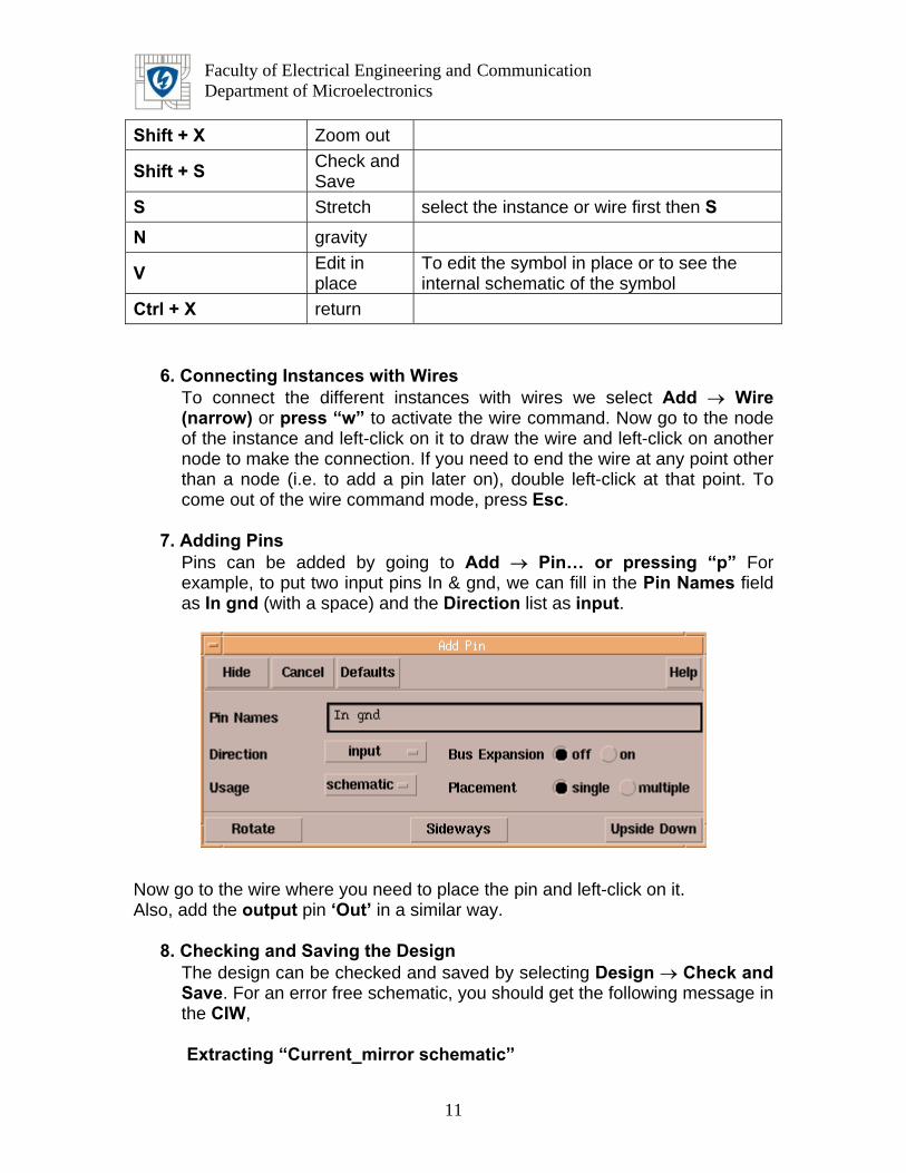
5. Command Functions Some common command modes and functions are available under Add and Edit menus, the most used command are mentioned in the following table:
Keyboard shortcut Function Remark I Instance to add instance to schematic
Q Property select the instance you want to edit first
W Wire
M Move select the instance you want to move first
C Copy select the instance you want to copy first
G Mirror ↕ select the instance, press M first then G
Shift + G Mirror ↔ select the instance, press M first then G
Ctrl + W Rotate select the instance, press M first then G
P Pin
A Select
Ctrl + A Select All
D Deselect
Ctrl + D Deselect All
U Undo
Shift + U Redo
F Fit
Z Zoom in
10
Faculty of Electrical Engineering and Communication Department of Microelectronics
Shift + X Zoom out
Shift + S Check and Save
S Stretch select the instance or wire first then S
N gravity
V Edit in place
To edit the symbol in place or to see the internal schematic of the symbol
Ctrl + X return 6. Connecting Instances with Wires
To connect the different instances with wires we select Add → Wire (narrow) or press “w” to activate the wire command. Now go to the node of the instance and left-click on it to draw the wire and left-click on another node to make the connection. If you need to end the wire at any point other than a node (i.e. to add a pin later on), double left-click at that point. To come out of the wire command mode, press Esc.
7. Adding Pins
Pins can be added by going to Add → Pin… or pressing “p” For example, to put two input pins In & gnd, we can fill in the Pin Names field as In gnd (with a space) and the Direction list as input.
Now go to the wire where you need to place the pin and left-click on it. Also, add the output pin ‘Out’ in a similar way.
8. Checking and Saving the Design The design can be checked and saved by selecting Design → Check and Save. For an error free schematic, you should get the following message in the CIW,
Extracting “Current_mirror schematic”
11

Faculty of Electrical Engineering and Communication Department of Microelectronics
Schematic check completed with no errors. ”Current_mirror Current_mirror schematic” saved.
Note: The CIW should not show any warnings or errors when you check and save.
9. Using all the commands given above the schematic of a Current_mirror can be constructed as shown below.
12

Faculty of Electrical Engineering and Communication Department of Microelectronics
10. After saving the design with no errors, select Window → Close. 2.2 Creating a Symbol View of the Current_mirror You have now created a schematic view of your Current_mirror. Now you need to create a symbol view if you want to use that circuit in a different schematic.
1. In the Virtuoso schematic window of the schematic you have created above, select Design → Create Cellview → From CellView... A Cell View from Cell View window appears, press OK.
2. In the Symbol Generation Options window you can define which Pins
are Left, Right, Top or Bottom, then press OK.
13

Faculty of Electrical Engineering and Communication Department of Microelectronics
2. In the Virtuoso Symbol Editing window that appears, make modificationsto make the symbol look as below. Replace [@partname] with the name Current_mirror. You may delete [@instanceName]. Save the symbol and exit using Window → Close.
3. Now the Current_mirror is ready to be used in other schematics.
14

Faculty of Electrical Engineering and Communication Department of Microelectronics
3 Analysis In the Schematic Editor, select Tools → Analog Environment. In the Cadence@ Analog Design Environment Simulation Window that appears.
the Cadence@ Analog Design Environment Window select Analyses a hoosing Analyses appear, there are many kinds of simulators and analysis ethods. So all that you need to do in this window is to select the type of
analysis you need and then select the nodes at which you want to observe the waveforms. You are encouraged to play around with the various menus and figure out how they make can your analysis easy and interesting.
InCm
15

Faculty of Electrical Engineering and Communication Department of Microelectronics
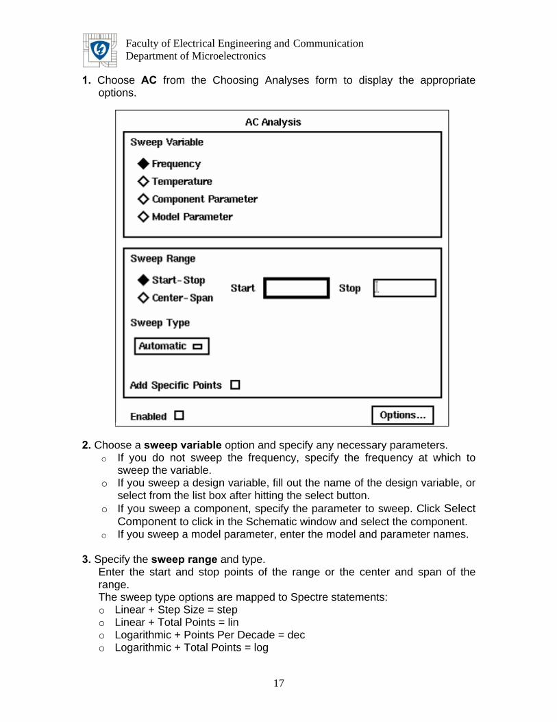
3.1 AC Small-Signal Analysis AC small-signal analysis linearizes the circuit about the DC operating point and computes the response to a given small sinusoidal stimulus. Spectre can perform the analysis while sweeping a parameter. The parameter can be a frequency, a design variable, temperature, a component instance parameter, or a component model parameter. If changing a parameter ffects the DC operating point, the operating point is recomputed on each step. a
To set up an AC small-signal analysis,
16
Faculty of Electrical Engineering and Communication Department of Microelectronics
1. Choose e appropriate options.
specify any necessary parameters. o If you do not sweep the frequency, specify the frequency at which to
sweep the variable. o If you sweep a design variable, fill out the name of the design variable, or
select from the list box after hitting the select button. o If you sweep a component, specify the parameter to sweep. Click Select
Component to click in the Schematic window and select the component. o If you sweep a model parameter, enter the model and parameter names.
3. Specify the sweep range and type.
Enter the start and stop points of the range or the center and span of the range. The sweep type options are mapped to Spectre statements: o Linear + Step Size = step o Linear + Total Points = lin o Logarithmic + Points Per Decade = dec o Logarithmic + Total Points = log
AC from the Choosing Analyses form to display th
2. Choose a sweep variable option and
17

Faculty of Electrical Engineering and Communication Department of Microelectronics
o Add Specific Points = values=[…]
. Click Options to select the Spectre options controlling the simulation.
. Click Enable and Apply.
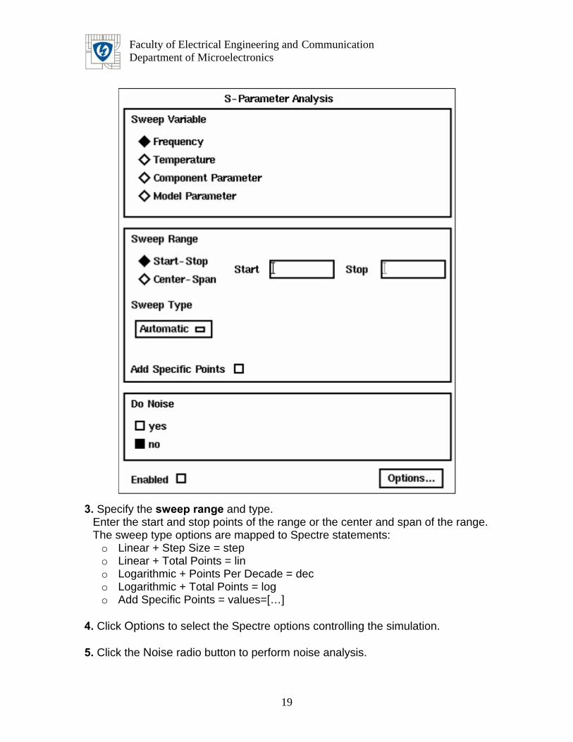
.2 S-Parameter Analysis he S-parameter analysis linearizes the circuit about the DC operating point and omputes S-parameters of the circuit taken as an N-port. The psin instances etlist-to-Spectre port statements) define the ports of the circuit. Each active port turned on sequentially, and a linear small-signal analysis is performed. The pectre simulator converts the response of the circuit at each active port into S-arameters and prints these parameters. There must be at least one active port nalogLib psin instance) in the circuit.
he parameter can be a frequency, a design variable, temperature, a component stance parameter, or a component model parameter. If changing a parameter ffects the DC operating point, the operating point is recomputed on each step. o set up an S-parameter analysis,
. Choose sp from the Choosing Analyses form to display the appropriate options.
. Choose a sweep variable option and specify any necessary parameters. o If you do not sweep the frequency, specify the frequency at which to
sweep the variable. o If you sweep a design variable, fill out the name of the design variable, or
select from the list box after hitting the select button. If you sweep a component, specify the parameter to sweep. Click Select
4 5 3Tc(nisSp(aTinaT 1
2
oComponent to select the component in the Schematic window.
o If you sweep a model parameter, enter the model and parameter names.
18
Faculty of Electrical Engineering and Communication Department of Microelectronics
3. Specify the sweep range and type.
Enter the start and stop points of the range or the center and span of the range. The sweep type options are mapped to Spectre statements:
o Linear + Step Size = step o Linear + Total Points = lin o Logarithmic + Points Per Decade = dec o Logarithmic + Total Points = log o Add Specific Points = values=[…]
4. Click Options to select the Spectre options controlling the simulation. 5. Click the Noise radio button to perform noise analysis.
19

Faculty of Electrical Engineering and Communication Department of Microelectronics
6. Click Enabled and Apply
.3 DC Analysis he DC analysis finds the DC operating point or DC transfer curves of the circuit. o generate transfer curves, specify a parameter and a sweep range. The arameter can be a temperature, a device instance parameter, or a device model arameter.
weeping a Variable o run a DC transfer curve analysis and sweep a variable, 1. Choose a sweep variable.
The Choosing Analyses form redisplays to show additional fields.
design variable, or er pressing the select button.
ponent name and the parameter
nd to click in the Schematic window to
ents:
3TTpp
To save the DC operating point,
Click Save DC Operating Point, click Enabled, and click Apply ST
2. Specify the necessary parameters. iable, fill out the name of the o If you sweep a design var
choose from the list box afto To sweep a component, specify the com
to sweep. o Use the select componentcomma
select the component. o To sweep a model parameter, enter the model and parameter names.
3. Specify the sweep range and type.
The sweep type options are mapped to Spectre statem
20
Faculty of Electrical Engineering and Communication Department of Microelectronics
o Linear + Step Size = step o Linear + Total Points = lin
ints Per Decade = dec
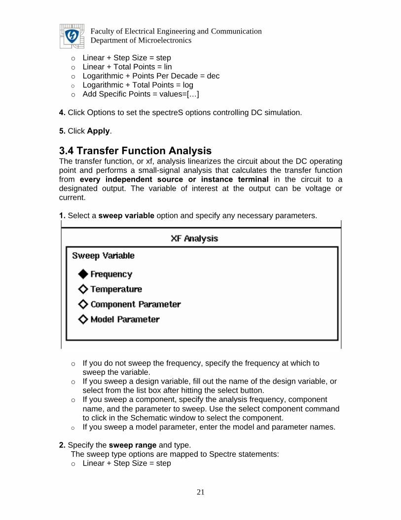
5. Click Apply. 3.4 Transfer Function Analysis The transfer function, or xf, analysis linearizes the circuit about the DC operating point and performs a small-signal analysis that calculates the transfer function from every independent source or instance terminal in the circuit to a designated output. The variable of interest at the output can be voltage or current. 1. Select a sweep variable option and specify any necessary parameters.
. Specify the and type. to Spectre statements:
o Logarithmic + Po Logarithmic + Toto al Points = log
o Add Specific Points = values=[…] 4. Click Options to set the spectreS options controlling DC simulation.
o If you do not sweep the frequency, specify the frequency at which to
sweep the variable. o If you sweep a design variable, fill out the name of the design variable, or
select from the list box after hitting the select button. o If you sweep a component, specify the analysis frequency, component
name, and the parameter to sweep. Use the to click in the Schematic window to select the component. If you sweep a model p
select component command
o arameter, enter the model and parameter names. 2 sweep range
The sweep type options are mappedo Linear + Step Size = step
21

Faculty of Electrical Engineering and Communication Department of Microelectronics
o Linear + Total Points = lin o Logarithmic + Points Per Decade = dec
]
ic tion sim 5. Clic
o Logarithmic + Total Points = log o Add Specific Points = values=[…
3. Choose voltage or current for Output.
o To measure the output voltage, click Select opposite Positive Output Node and click a net in the schematic.
o To measure the output current, click current, click Select opposite Negative Output Node, and click an instance in the schematic.
4. Cl ng transfer funculation.
k Apply.
k Options to set the spectreS options controlli
22

Faculty of Electrical Engineering and Communication Department of Microelectronics
3.5The nd com e output. If you specify an input pro , t-referred noise for an equivalent noise-free network is computed. To set up a noise analysis, 1. Choose a sweep variable option and specify any necessary parameters.
ing the select button.
2. Specify the sweep range and type.
Noise Analysis noise analysis linearizes the circuit about the DC operating point aputes the totalnoise spectral density at th
be the transfer function and the inpu
o If you do not sweep the frequency, specify the frequency at which to
sweep the variable. o If you sweep a design variable, fill out the name of the design variable, or
choose from the list box after presso If you sweep a component, specify the analysis frequency, component
name, and the parameter to sweep. Use the select component command to click in the Schematic window to select the component.
o If you sweep a model parameter, enter the model and parameter names.
23

Faculty of Electrical Engineering and Communication Department of Microelectronics
The sweep type options are mapped to Spectre statements:
oChoose an Output Noise option.
o itive
4. O
o
Apply.
5. Click Options to set the spectreS options controlling noise simulation. 6. Click Apply. 3.6 Sensitivity Analysis Sensitivity analysis lets a designer see which parameters in a circuit most affect the specified outputs. It is typically used to tune a design to increase or decrease certain design goals. You might run a sensitivity analysis to determine which parameters to optimize using the optimizer. 1. Choose the sens radio button on the Choosing Analyses form. The form
redraws:
o Linear + Step Size = step o Linear + Total Points = lin o Logarithmic + Points Per Decade = dec o Logarithmic + Total Points = log
Add Specific Points = values=[…] 3.
To measure the output noise voltage, click Select opposite Pos
Output Node and click a net in the schematic. o To measure the output noise current, click current, click Select opposite
Negative Output Node, and click a voltage source in the schematic.
ptionally, choose an Input Noise option. o Choose voltage, current, or port.
Click Select Input. o Click a source or port in the schematic. o Click
24

Faculty of Electrical Engineering and Communication Department of Microelectronics
2. C you want to calculate.
the For base field, choose any of the analyses on which you want to perating
point), dc, and ac. un a sensitivity analysis, you must run the corresponding base
analysis.
The Schematic window must be
. (Optional) In the Simulation window, choose Simulation – Options to open the Simulator Options form. Scroll down in the form to find the sensitivity options.
hoose which types of sensitivitiesInperform a sensitivity analysis. The available analyses are dcOp(DC o
Before you r
3. Click Select to select the outputs you want to measure.
Select prompts you to select outputs by clicking on their instance in the schematic. Outputs can be any nets or ports. When you click Select, the Schematic window moves to the front of the screen.open before you can select any outputs. Use the Esc key to end selection.
4
25

Faculty of Electrical Engineering and Communication Department of Microelectronics
Type a filename in the sensfile field to specify a filename for the Spectre ensitivity results. This file is in ASCII format, and is generated in the psf irectory. If you do not specify a value, the file is named sens.output by default.
. View your results. From the simulation window, choose Results – Print – Sensitivity. The results display in a print window.
Thecomranges of specified values. You can display the results of the analysis as charts or plo eters.
fter running a parametric analysis, you can plot a group of curves for any ch curve represents
thedifferent curves to choose the best value. Frocan
sd 5
3.7 Parametric Analysis
parametric analysis feature (parametric plotting) lets you assign values to ponents and other parameters in a circuit and sweep the circuit over the
different types of curves, depending on the values assigned to the axis and tting param
Awaveform object in the netlist in a single display window. Ea
results for a particular value in the sweep range, and you can compare the
m the Affirma Analog Circuit Design Environment Simulation Window, you use the following procedure to call up the Parametric Analysis window:
Choose Tools → Parametric Analysis in the Affirma analog circuitsimulation window.
26

Faculty of Electrical Engineering and Communication Department of Microelectronics
The Parametric Analysis window appears. You use this window to specify values for the parametric analysis. You can enter many specifications, and you can hoose options from three main menus at the top of the window. These menuc s
Analysis.
3.8 Corners Analysis The corners tool provides a convenient way to measure circuit performance while simulating a circuit with sets of parameter values that represent the most extreme variations in a manufacturing process. With the tool, you can compare the results for each set of parameter values with the range of acceptable values. By revising the circuit, if necessary, so that all the sets of parameters produce acceptable results, you can ensure the largest possible yield of circuits at the end of the manufacturing process. To prepare for a corners analysis,
Ensure that the design you use is simulatable with nominal design parameter values.
irtuoso® Analog Design Environment window
are Tool, Setup, and
Set up a simulation in the Vto run the analysis you want to use.
Ensure that all design variables in the circuit have an initial value. In the Virtuoso Analog Design Environment window, choose Tools →
ADS → Cornertool…
27

Faculty of Electrical Engineering and Communication Department of Microelectronics
3.9 Other Analysis’s
alyses Periodic AC (PAC) analysis Periodic S-Parameter (PSP) analysis Periodic Transfer Function (PXF) analysis Periodic Noise (Pnoise) analysis
o Periodic Distortion (Pdisto) analysis o Quasi-Periodic Noise (QPnoise) analysis o Envelope Following analysis
Periodic Steady-State (PSS) analysis is a large-signal analysis that directly
mputes the periodic steady-state response of a circuit. With PSS, simulation mes are independent of the time constants of the circuit, so PSS can quickly
onse of circuits with long time constants, such as
pectreRF simulator can model frequency
to the Spectre C, SP, XF, and Noise analyses, but you can apply them to periodically driven
nversion. Examples of important frequency onversion effects include conversion gain in mixers, noise in oscillators, and
filteTherefore, with Periodic Small-Signal analyses you apply a small signal at a freqperiod m, the clock. This small signal is ass Perio ts
th m l ith Pdisto, you can model periodic distortion and lude harmonic effects.
(Periodic small-signal analyses assume the small signal you specify generates no harmonics). Pdisto computes both a large signal, the periodic steady-state response of the circuit, and also the distortion effects of a specified number of moderate signals, including the distortion effects of the number of harmonics that you choose. With Pdisto, you can apply one or two additional signals at frequencies not harmonically related to the large signal, and these signals can be large enough to create distortion. This analysis is also called Quasi-Periodic Steady-State analysis.
The SpectreRF analyses add several kinds of functionality to Spectre simulation.
o Periodic Steady-State (PSS) analysis o Periodic Small-Signal an
coticompute the steady-state resphigh-Q filters and oscillators. You can perform sweeps using PSS; you can sweep frequency, a time period, or a variable. After completing a PSS analysis, the Sconversion effects by performing one or more Periodic Small-Signal analyses (PAC, PSP, PXF, and Pnoise). The periodic small-signal analyses, Periodic AC analysis (PAC), Periodic SParameter analysis (PSP), Periodic Transfer Function analysis (PXF) and Periodic Noise analysis (Pnoise), are similarAcircuits that exhibit frequency coc
ring using switched-capacitors.
uency that may not be harmonically related (noncommensurate) to the ic response of the undriven syste
umed to be small enough so that it is not distorted by the circuit.
dic Distortion (Pdisto) analysis, a large-signal analysis, is used for circui ultiple arge tones. Wwi
inc
28

Faculty of Electrical Engineering and Communication Department of Microelectronics
4 About the Saved, Plotted, and Marched Sets of
The t keeps track of three sets of nets and
• The saved set, for which simulation data is written to disk • T after simulation in the
W expressions. the Marching Waveform window
ill be plotted and two will be saved after
the Setting utputs form.
Outputs Affirma analog circuit design environmen terminals:
he plotted set, which is automatically plottedaveform window the plotted set can also contain
• The marched set, which is plotted induring simulation
In the figure below, all five signals wsimulation. None will be marched during simulation.
Opening the Setting Outputs Form You set up the saved, plotted, and marched sets of outputs withO
In the Simulation window, choose Outputs → Setup, or from the Schematic window, choose Setup → Outputs.
29

Faculty of Electrical Engineering and Communication Department of Microelectronics
Saving All Voltages or Currents To save all of the node voltages and terminal currents,
1. In the Simulation window, choose Outputs → Save All, or in the Schematic window, choose Setup → Save All.
2. Select the values you want to save and click OK.
Note: When you set up a noise analysis with cdsSpice only, the system turns these options off. If you later deactivate the noise analysis, the system reactivates the Select all options. Saving Selected Voltages or Currents To save the simulation data for particular nodes and terminals,
1. In the Simulation window, choose Outputs → To Be Saved → Select on Schematic, or in the Schematic window, choose Setup → Select on
aved.
rminals. Click on the square pin symbols to choose currents. Click on wires to choose voltages. Click and drag to choose voltages by area.
Schematic → Outputs to be S 2. In the Schematic window, choose one or more nodes or terminals. The
system circles pins when you choose a current and highlights wires when you choose a net.
Click on an instance to choose all instance te
30

Faculty of Electrical Engineering and Communication Department of Microelectronics
3. Press the Esc key when you finish.
Removing Nodes and Terminals from a Set To remove a node or terminal from the saved, plotted, or marched set,
3. In the Simulation window, choose Outputs → Setup, or in the Schematic utputs.
Of Outputs list box.
o highlight the node in the Sim
nsconductance (gm) etc. are also of Circuit Design
Pointswindow
window, choose Setup → O4. Double-click on the node or terminal in the Table5. Click to deselect the appropriate Will Be boxes. 6. Click Change.
N te: To remove a node from all three sets (delete it),
lation window and choose Outputs – Delete. u
howing DC Properties SExcept node voltages, DC currents, traconcern. To see these parameters, from the Affirma AnalogEnvironment Simulation Window choose Results → Print → DC Operating
, and then click on the Instance in the Virtuoso Schematic Editing . A new window shows the DC properties will pop up.
31

Faculty of Electrical Engineering and Communication Department of Microelectronics
32
5 About the Calculator
In the Affirma Analog Circuit Design Environment Simulation Window choose Tool → Calculator. The calculator has several kinds of buttons.
o Use the Results Browser to select results out of the UNIX file system hierarchy
o Use the wave command to select a curve in the Waveform Window
Selecting Data There are three ways to bring simulation results into the calculator. You can
o Use the schematic expression keys to click nets and pins in the schematic and select their results

Faculty of Electrical Engineering and Communication Department of Microelectronics
Selecting Data in a Schematic Window The schematic expression keys let you enter data into the calculator buffer by selecting objects in the Schematic window. Note: To use the vn, var, op, opt, or mp functions, you must either select results or have just run a simulation. vt transient voltage it transient current
vf frequency voltage if frequency current
vs source sweep voltage is source sweep current (I vs V curves)
vdc DC voltage op DC operating point
vn ino se voltage opt transient operating point
var design variable mp model parameter
1. Click a schematic expression key. 2. Click the appropriate object in the schematic.
If more than one parameter is available for the expression and instance you picked, a form appears. Select the parameter you want from the List field and click OK.
3. When you have finished selecting objects, press the Esc key while the cursor is in the Schematic window.
Choosing Parameters from Schematic Data To select a parameter in the schematic with a schematic expression key
33

Faculty of Electrical Engineering and Communication Department of Microelectronics
1. Click an instance in the schematic. 2. Choose the parameter you want from the List field.
the op, opt, mp, vn, must have just run must choose selec sults menu in the therwise, the system t to display.
rrents s in the schematic . e pin symbols, not wires
ou c estrict selection to either pins or wires. ress F3 if the Selection Filter form did not appear.
34
Note: When you use or var functions, youa simulation, or you Simulation window. O
t results from the Re does not know wha
Choosing Voltages or CuTo select voltage
Click wiresTo select currents
Click squar .
YP
an use the Selection Filter form to r
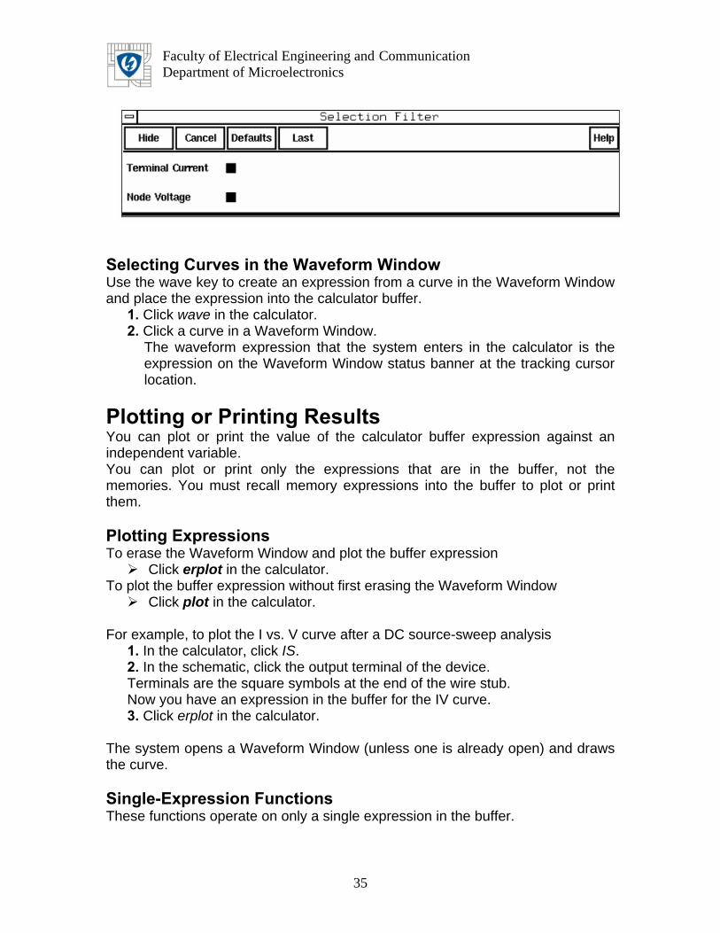
Faculty of Electrical Engineering and Communication Department of Microelectronics
Selecting Curves in the Waveform Window Use the wave key to create an expression from a curve in the Waveform Window nd place the expression into the calculator buffer.
1. Click wave in the calculator. 2. Click a curve in a Waveform Window.
The waveform expression that the system enters in the calculator is the expression on the Waveform Window status banner at the tracking cursor location.
lotting or Printing Results ou can plot or print the value of the calculator buffer expression against an
To erase the Waveform Window and plot the buffer expression in the calculator.
To sing the Waveform Window Click plot in the calculator.
For example, to plot the I vs. V curve after a DC source-sweep analysis
1. In the calculator, click IS. 2. In the schematic, click the output terminal of the device. Terminals are the square symbols at the end of the wire stub. Now you have an expression in the buffer for the IV curve. 3. Click erplot in the calculator.
he system opens a Waveform Window (unless one is already open) and draws
Single-Expression Functions These functions operate on only a single expression in the buffer.
a
PYindependent variable. You can plot or print only the expressions that are in the buffer, not the memories. You must recall memory expressions into the buffer to plot or print
em. th Plotting Expressions
Click erplot plot the buffer expression without first era
Tthe curve.
35

Faculty of Electrical Engineering and Communication Department of Microelectronics
Key Function Key Function mag magnitude exp ex
phase phase 10**x 10x
real real component y**x yx
imag imaginary component
x**2 x2
ln base-e (natural) logarithm
abs |x| (absolute value)
log10 base-10 logarithm int integer value dB10 dB magnitude for 1/x
a power expression
inverse
dB2 0 dB magnitude for a
sqrt x
voltage or current
gnitude of a Signal AC analysis
the Schematic window, press the Esc key.
calculator buffer now contains the expression you want to plot. 5. Click plot to show the curve.
Example: Plotting the MaTo plot the dB magnitude of a signal after an
1. Click vf on the calculator. 2. On the schematic, click the net you want to plot. 3. With the cursor inThis cancels the vf function. Otherwise, the command stays active. 4. Click dB20 on the calculator. The
36
Faculty of Electrical Engineering and Communication Department of Microelectronics
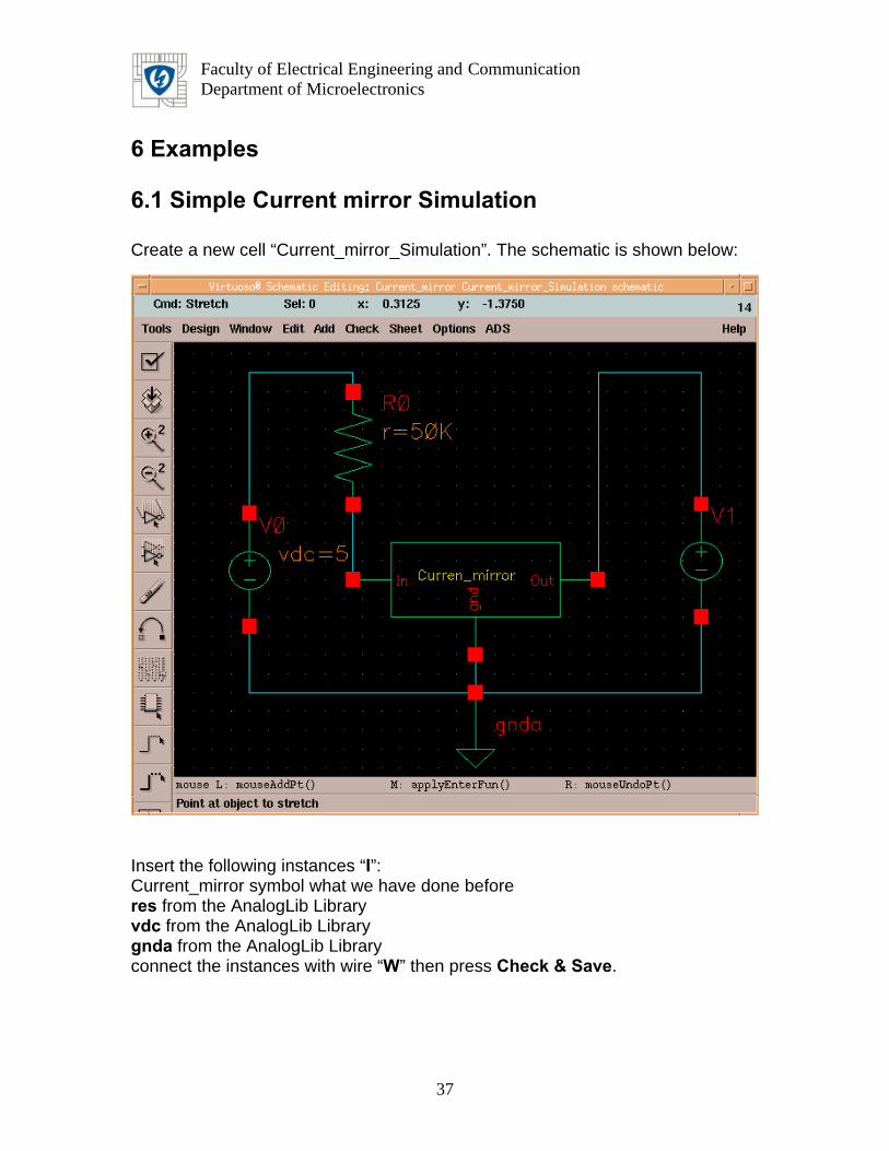
6 Examples
imple Cur im ion
Create a new cell “Current_mirror_Simulation”. The schematic is shown below:
Insert the following instances “I”: Current_mirror symbol what we have done before res rom the AnalogLib Library vdc ogLib Library gnda from the AnalogLib Library connect the instances with wire “W” then press Check & Save.
6.1 S rent mirror S ulat
f from the Anal
37

Faculty of Electrical Engineering and Communication Department of Microelectronics
38
Notice: The most used libraries are: AnalogLib for instances used for simulation purpose such: resistor, capacitor, voltage and current supply,… TransistorLib for instances related to the used technology as: transistors, resistors (type: hipo, nwell, Rdummy, poly,..), capacitors (typ: Cdummy, cpp,..) Printing your Schematic Now that the schematic is complete, you could print it out. To do this, in the Virtuoso Schematic Editing window, choose Design → Plot → Submit... The submit plot window appear.

Faculty of Electrical Engineering and Communication Department of Microelectronics Faculty of Electrical Engineering and Communication Department of Microelectronics
39
Click Plot Options... The Plot Options subwindow appears.
Press window.
Check the "Send Plot Only To File" and type in a descriptive name about the plot. Be sure to end the name with the ".ps" or ".eps" extension, as seen above.What you are plotting is a postscript file. When the machine is done creating the file, it will send you mail telling you that it completed successfully. To prevent this, you can uncheck "Mail Log To".
Ok at Plot Options window and then press OK at submit plotNow the plot of your schematic is done.
39

Faculty of Electrical Engineering and Communication Department of Microelectronics
Simulator Setup nalog Environment
sta
C Simulation the Analog Design Environment window, choose Analyses → Choose, In e pop-up window, click on dc analysis and choose to Save DC Operating oint, select the Component Parameter then click on Select Component then ou can choose the component you want to sweep directly from the schematic, in ur case the dc parameter of V1, then click OK.
In Virtuoso Schematic Editing window, choose Tools → Art the simulation tool Analog Design Environment to
DInthPyo
40

Faculty of Electrical Engineering and Communication Department of Microelectronics
In the Analog Design Environment window, choose Outputs → To Be Plotted → Select On Schematic. In the Schematic Editing window click on the
rminals In and Out of the Current mirror, then click Esc. In the Outputs of the esign Environment on appears I1/In and I1/Out.
ow you c Warning message to save the outputs before simulating, click Yes.
teCadence Analog D Na
an run the simulation: Simulation → Netlist and Run or press
Choose Design…
Choose Analyses…
Edit Variables…
Setup Outputs…
Delete
Netlist & Run
Run
Plot Outputs
41

Faculty of Electrical Engineering and Communication Department of Microelectronics
Delete
Move
Undo
Crosshair marker A
Crosshair marker B
alculatoC
r
Switch is mode
Add Subwindow
You can split the wave form by pressing Switch Axis mode
Ax
o display Grid to Waveform Window, press Axes → Options… andrid then press OK.
o read some value on the Waveform Window choose Croohair marker A
T check G T eventually B.
42

Faculty of Electrical Engineering and Communication Department of Microelectronics
Printing out your waveform: At Waveform Window press Windows → Hardcopy …, enable Send Plot Only
o File, and type in a descriptive name about the plot. Be sure to end the name it ".ps" or ".eps" extension. Later you can see the plot with ps browser ols.
C operating points: Except node voltages, DC currents, transconductance (gm) etc. are also of concern. To see these parameters, from the Analog Design Environment window, choose Results → Print → DC Operating Points, and then click on the instance in the “Schematic Editing” window. A new window as below will pop up.
Tw h the to D
43

Faculty of Electrical Engineering and Communication Department of Microelectronics
To see the DC operating point of the M_NMOS transistor of the current_mirror symbol, Now you choose in the same way: Results → Print first click on it and then press “V”
→ DC Operating Points, and then click on the instance in the “Schematic Editing” window. A new window as below will pop up
44

Faculty of Electrical Engineering and Communication Department of Microelectronics
Corners Analyses: In the Virtuoso Analog Design Environment window, choose Tools → ADS → Cornertool…, Start Corner Analysis window appears, click Save and chooce the File Name where you want to save the corner analyses result (usally copy
Press OK on the Ok on the Start Corner Anlysis
Choose Add Variable to add temperuter then press Generat Corners.
the path and paste it on the File Name).
Save Ocean Script to File window then window.
45

Faculty of Electrical Engineering and Communication Department of Microelectronics
Now you can select one or more cases for each device and the temperature sweep then press Generat Corners.
46

Faculty of Electrical Engineering and Communication Department of Microelectronics
Press Simulation → Run then OK.
Parametric Analysis: In Virtuoso Schematic Editing window, choose the instance for parametricanalysis, for example R0, select R0 press “Q” to open the Edit Object Properties window, on the Resistance filed type “Rvar” for example, press OK then Check and Save.
47

Faculty of Electrical Engineering and Communication Department of Microelectronics
From the Cadence Analog Design Environment Simulation Window, Choose Variable → Edit… In the Editing Design Variable window, type the name of the variable Rvar, ress OK. p
48
Faculty of Electrical Engineering and Communication Department of Microelectronics
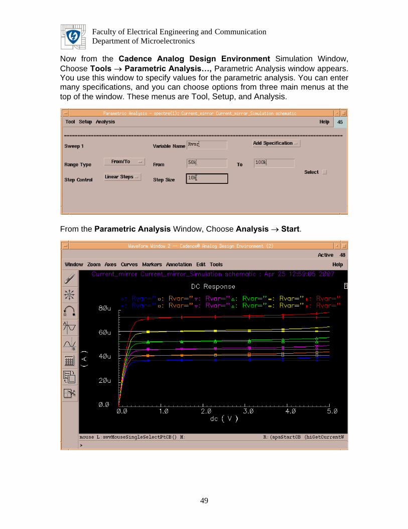
Now from the Cadence Analog Design Environment Simulation Window, Choose Tools → Parametric Analysis…, Parametric Analysis window appears. You use this window to specify values for the parametric analysis. You can enter many specifications, and you can choose options from three main menus at the top of the window. These menus are Tool, Setup, and Analysis.
From the Parametric Analysis Window, Choose Analysis → Start.
49

Faculty of Electrical Engineering and Communication Department of Microelectronics
6.2 Single-ended Operational Transconductance Amplifier
Signal source connection: Vdc=1V in series with a vsin, whose AC magnitude is 1V. Two vcvs are connected to the vsin. The gains are set to be 0.5 and -0.5 for vinp and vinn respectively. DC Simulation Run DC simulation and check the operating points (node voltage, branch current, transistor parameters). Fine tune the transistor size to meet the design specifications.
50

Faculty of Electrical Engineering and Communication Department of Microelectronics
AC Simulation
ne, choose Results → Direct Plot → AC Magnitude & Phase in esign Environment. Then click on the wire connected to the top
Set the AC simulation then run the simulation. When the simulation is successfully dohe Analog Dtplate of the capacitor and press Esc. A Bode plot will show the AC response of the amplifier. Click on the “Switch Axis Mode” button to separate the plots.
51

Faculty of Electrical Engineering and Communication Department of Microelectronics
Transient Response Transient response is used to analyze the SR of the OTA. Connect the OTA as a voltage buffer. Apply a vpulse (0.9 -1.8V). The pulse period is set to be 10us and width is 5us. Run transient simulation, plot the output and measure the SR of both rising edge and falling edge.
52

Faculty of Electrical Engineering and Communication Department of Microelectronics
53

Faculty of Electrical Engineering and Communication Department of Microelectronics
54
Faculty of Electrical Engineering and Communication Department of Microelectronics
54
7 Reference [1] Cadence Design Systems, Affirma™ Analog Circuit Design Environment User
Guide [2] Cadence Design Systems, Analog IC Design Tutorial for Schematic Design
and Analysis using Spectre [3] Cadence Design Systems, Waveform Calculator User Guide [4] Cadence Design Systems, Virtuoso® Schematic Composer Tutorial [5] Cadence Design Systems, Virtuoso® Advanced Analysis Tools User Guide [6] Cadence Design Systems, Cadence SPICE™ Reference Manual [7] Cadence Design Systems, Affirma RF Simulator User Guide [8] Cadence Design Systems, Affirma™ Verilog®-A Language Reference [9] AMS CMOS IC Design, Dr. Sameer Sonkusale