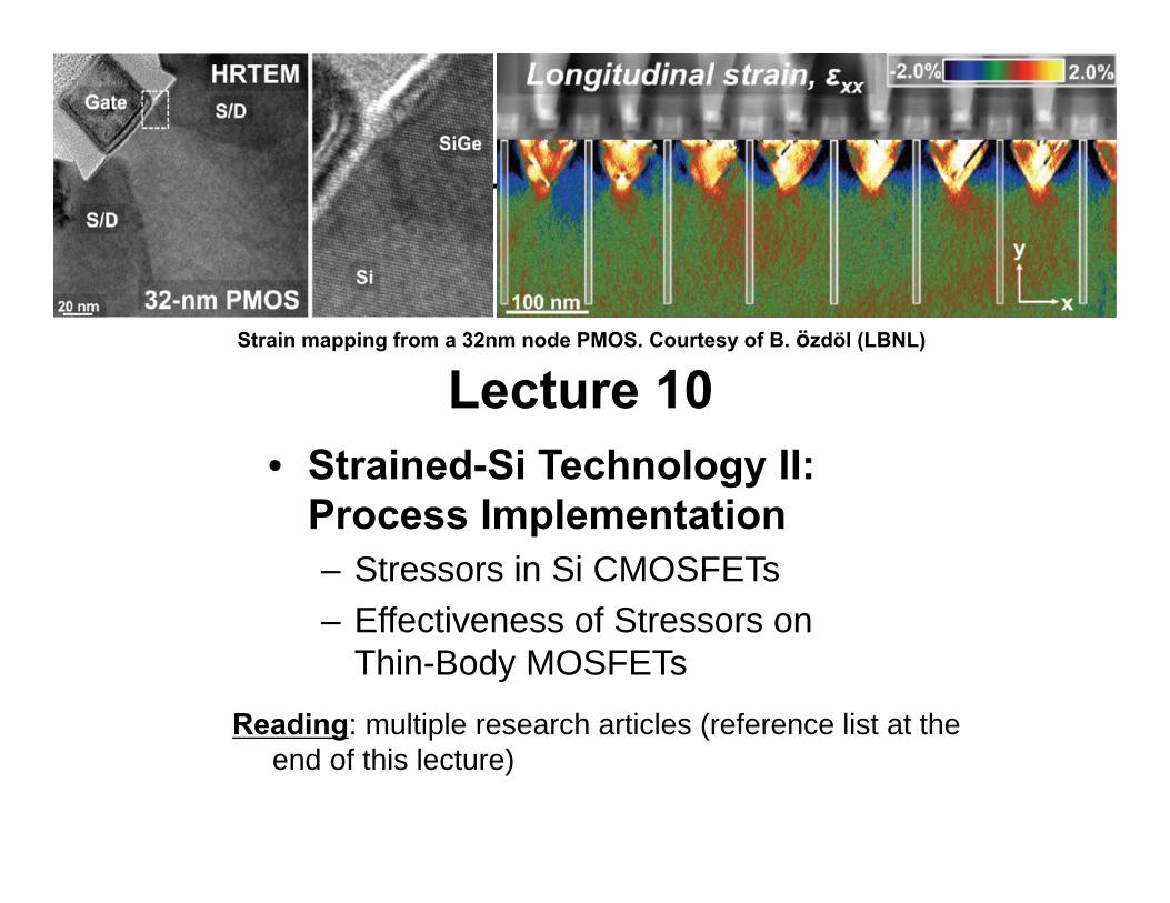
strain mapping from a 32nm node pmos. courtesy of b. …ee290d/fa13/lecturenotes/lecture10.pdf ·...
TRANSCRIPT
Lecture 10• Strained-Si Technology II:
Process Implementation– Stressors in Si CMOSFETs– Effectiveness of Stressors on
Thin-Body MOSFETs
Reading: multiple research articles (reference list at the end of this lecture)
Strain mapping from a 32nm node PMOS. Courtesy of B. özdöl (LBNL)
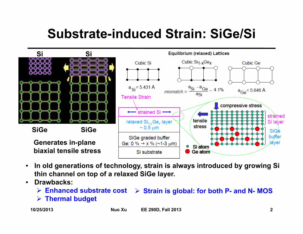
Substrate-induced Strain: SiGe/Si
10/25/2013 2Nuo Xu EE 290D, Fall 2013
• In old generations of technology, strain is always introduced by growing Si thin channel on top of a relaxed SiGe layer.
• Drawbacks: Enhanced substrate cost Thermal budget
Strain is global: for both P- and N- MOS
Si Si
SiGe SiGe
Generates in-plane biaxial tensile stress

Embedded Source/Drain Stressor: SiGe for PMOS
10/25/2013 3Nuo Xu EE 290D, Fall 2013
• Resulting longitudinal compressive + vertical tensile stress
• Pros: Cheaper than substrate strain Local, does not affect NMOS More effective to hole
• Cons: Worsens BTBT junction leakage Too high Ge% causes reliability
problems by introducing defects
(major)
K. Mistry, VLSI (2004)

Evolution of eSiGe S/D Technology
10/25/2013 4Nuo Xu EE 290D, Fall 2013
Intel’s eSiGe S/D Technology
90nm 45nm 32nm 22nm
U-shape Faceted Shape Raised S/D
18% 22% 30% 40% 55%
Fin S/D
55nm 32nm 25nm 20nm 18nm
65nm
Deeper Recess
Gate-Last Approach Tri-Gate
Gate Pitch Shrinks
Increased Ge Mole Fraction
Increased SiGe S/D Proximity
C. Auth, VLSI (2008)K. Mistry, VLSI (2004) P. Packan, IEDM (2009) C. Auth, VLSI (2012)
Ge%:
S/D-Gate spacing:
otherknobs:

Embedded Source/Drain Stressor: Si:C for NMOS
10/25/2013 5Nuo Xu EE 290D, Fall 2013
TEM View and Gm of NMOSFET w/ Si:C S/D
• Resulting longitudinal tensile + vertical compressive stress→ Good for NMOS mobility
• A barrier forms at Source/channel interface for electrons→ Reduced drain current at low VDS
(major)
K. W. Ang, IEDM (2004)

Strained Contact-Etch-Stop-Liner (CESL) Technology
10/25/2013 6Nuo Xu EE 290D, Fall 2013
• NMOS: Longitudinal tensile + vertical compressive stress• PMOS: Longitudinal compressive + vertical tensile stress
IBM’s Dual-strained CESL Technology
H.-S. Yang, IEDM (2004)
• Pros: Easy to integrate (low thermal budget) No reliability or performance degradation issues
• Cons: Low stress transfer efficiency

Stress Memorization Technology (SMT): Source/Drain
10/25/2013 7Nuo Xu EE 290D, Fall 2013
K. Y. Lim, IEDM (2009)
• Resulting longitudinal tensile + Vertical Compressive stress→ Good for NMOS mobility
• Amorphized S/D will not be fully recovered when Si volume is shrunk.→ Not applicable to thin-body MOSFETs
(major)

Stress Memorization Technology (SMT): Poly-Si Gate
10/25/2013 8Nuo Xu EE 290D, Fall 2013
K. Ota, IEDM (2002)
• Resulting vertical compressive + longitudinal tensile stress for As-doped poly-Si→ NMOS (electron) mobility enhanced; PMOS unaffected
• Not applicable to metal gate MOSFETs.
(major)

Impact of Metal-Gate-Last Processon Channel Strain
10/25/2013 9Nuo Xu EE 290D, Fall 2013
3. Dummy Gate Removal
4. Metal Gate Refill
2. CMP1. Deposition of CESL
• After poly-Si (dummy) gate removal, longitudinal stress (Sxx) is enhanced due to free boundary conditions to the S/D stressors; vertical stress (Szz) is reduced due to the loss of contacted surface from the gate.
A trade-off between Sxx and Szz
S. Mayuzumi, IEDM (2007)C. Auth, VLSI (2008)
Intel’s 45nm PMOS

Impact of Substrate on Channel Strain
10/25/2013 10Nuo Xu EE 290D, Fall 2013
SiGe
Si:C
BOXBOX
SiGe SiGe
SOI FinFETETSOI MOSFET TCAD Simulation
Raised S/D
LTO
HK
K. Cheng, IEDM (2009) V.S. Basker, VLSI (2010) V. Moroz, ECS Mtg. (2010)
• SOI MOSFET (planar or Fin-shape) cannot take advantage of the large stressor volume of the embedded Source/Drain.
• BOX region has larger stiffness than Si channel, which lowers the stress transfer efficiency.

Comparison of Stress Transfer Efficiency (STE)
10/25/2013 11Nuo Xu EE 290D, Fall 2013
• Embedded S/D (S/D SMT or eSiGe) stressor is most effective in longitudinal (x) direction.
• CESL stressor is most effective in vertical (z) direction.• Transverse stress (Syy) is always very small.
V. Moroz, ECS Mtg. (2010)
Longitudinal SxxVertical SzzTransverse Syy
≡

Strained-Silicon Technologies vs. Technology Generations
No longer effective due to reduced gate-pitch
still not in HVM yet..
Cannot be used to Fins or UTBsCannot be used to Metal-Gates
Courtesy of V. Moroz (Synopsys)
10/25/2013 12Nuo Xu EE 290D, Fall 2013
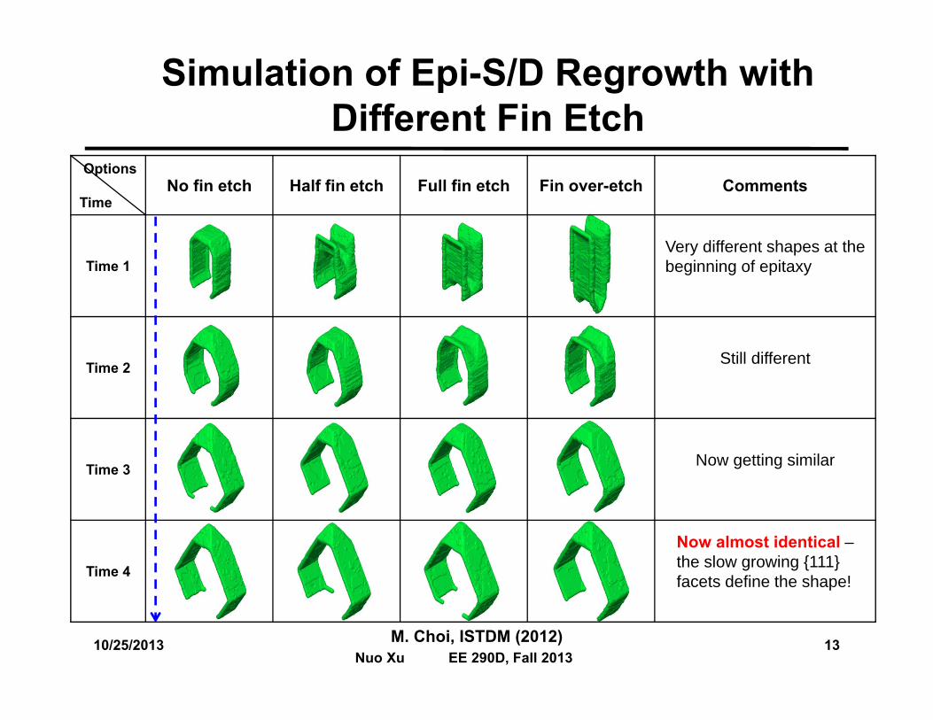
Simulation of Epi-S/D Regrowth with Different Fin Etch
Options
TimeNo fin etch Half fin etch Full fin etch Fin over-etch Comments
Time 1Very different shapes at the beginning of epitaxy
Time 2 Still different
Time 3 Now getting similar
Time 4
Now almost identical –the slow growing {111} facets define the shape!
10/25/2013 13Nuo Xu EE 290D, Fall 2013
M. Choi, ISTDM (2012)

Impact of SiGe-S/D Strain on Fin Etch
4 nm etch 16 nm etch 32 nm etch 48 nm etchSi0.5Ge0.5 Source/Drain (Intel’s 5th-gen strain Si tech. )
STI
ILD
Si fin
SiG
e
Gat
e
-462 MPa -1277 MPa -1462 MPa-815 MPa
• Deeper SiGe recess triples the channel stress!
Longitudinal Stress (SXX)
10/25/2013 14Nuo Xu EE 290D, Fall 2013M. Choi, ISTDM (2012)

Strained FinFETs Design Variations
(d)Metal Gate-First Metal Gate-Last
Bulk SubstrateSOI Substrate
• Various ways to introduce local uniaxial strain in advancedFinFET’s process.
10/25/2013 15Nuo Xu EE 290D, Fall 2013
N. Xu, TED (2012)

Stress in Aggressively scaled FinFETs
(d)Metal Gate-First Metal Gate-Last
Cha
nnel
Str
ess
(MPa
)
0
CESL SOI S/D Bulk S/D Bulk S/D
0
-300
500
300
-100
100SXX
SZZ
Bulk SubstrateSOI Substrate
• Longitudinal (Sxx) and Vertical (Szz) stress profiles alongFinFET’s channel in 17/12nm node.
Gate Last
10/25/2013 16Nuo Xu EE 290D, Fall 2013N. Xu, TED (2012)

FinFET Carrier Mobility Enhancement with S/D Stressors
10 15 20 25 30 350.0
0.2
0.4
0.6
0.8
1.0
1.2
1.4
15 20 25 30 35
h
/h
Open: Pinv=1e13cm-2 Closed: Pinv=5e12cm-2
Lg=17nm
Bulk,GateLast Bulk,GateFirst SOI,GateFirst
Ge Mole Fraction (%)
Lg=12nm
1.0 1.5 2.0 2.5 3.0 3.50.0
0.2
0.4
0.6
0.8
1.0
1.2
1.4
1.5 2.0 2.5 3.0 3.5
Open: Ninv=1e13cm-2 Closed: Ninv=5e12cm-2
e
/e
Lg=12nmLg=17nm
Bulk,GateLast Bulk,GateFirst SOI,GateFirst
C Mole Fraction (%)
N-Channel (Electron) P-Channel (Hole)
• Local uniaxial stress induced by faceted Si:C and SiGe S/D.
10/25/2013 17Nuo Xu EE 290D, Fall 2013
N. Xu, TED (2012)

0
10
20
30
40
50
[Khakifirooz 12]
[Cheng 09]
[Faynot 12]
[Zhang 05]
[Khakifirooz 12][Ernst 09]
[Faynot 10]
[Faynot 10]
[Andrieu 07]
[Andrieu 07]
[Andrieu 07]
[Andrieu 07]
[Fenouillet-Beranger 12]
[Ernst 09]
Wide WidthBiaxial Stress
I ON
Enh
ance
men
t (%
)
N-FDSOI P-FDSOI
OptimizedS/D Doping
SiGe S/DStrained SOI
strained CESL
[Andrieu 07]
Narrow WidthUniaxial Stress
• sCESL-induced enhancement is small.
• sSOI-induced enhancement is large for narrow-width nMOSFETs. Strain becomes
uniaxial after SOI etching
• Embedded-SiGe S/D is not effective unless raised-SiGe S/D is used.
Stress-Induced ION EnhancementFD-SOI MOSFETs
10/25/2013 18Nuo Xu EE 290D, Fall 2013
N. Xu, Int. SOI Conf. (2012)

Stress-Induced ION EnhancementFinFETs
0
10
20
30
40
50
[Yamashita 11]
[Yamashita 11]
[Basker 10]
[Verheyen 05][Chang 09]
[Mitra 11]
[Xiong 06]
[Wu 10]
[Ok 10]
Embeded S/D[Bufler 08]
OptimizedS/D Doping
SiGe S/DStrained SOI
N-FinFET P-FinFET
strained CESL
I ON E
nhan
cem
ent (
%)
• sCESL and sSOI can provide for significant enhancements.
• Embedded-SiGe S/D is the most effective for p-FinFETs.
• S/D doping must be optimized for maximum strain-enhancement.
10/25/2013 19Nuo Xu EE 290D, Fall 2013
N. Xu, Int. SOI Conf. (2012)

Volume-Change Stress Liners - A Way to Extend Strained-Si ?
10/25/2013 20Nuo Xu EE 290D, Fall 2013
by Prof. Y.-C. Yeo’s group (NUS)NMOS: ZnS-SiO2 PMOS: GST or GeTe
Y. Ding, IEDM (2011) & VLSI-T (2013)R. Cheng, VLSI-T (2012)

ReferencesPlanar MOSFET Stressors1. (Intel 90) K. Mistry, M. Armstrong, C. Auth, S. Cea, T. Coan et al., “Delaying Forever: Uniaxial
Strained Silicon Transistors in a 90nm CMOS Technology,” Symposium on VLSI Technology Dig.,pp.50-51, 2004.
2. (Intel 45) C. Auth, A. Cappellani, J.-S. Chun, A. Davis, T. Ghani et al., “45nm High-k+Metal GateStrain-Enhanced Transistors,” Symposium on VLSI Technology Dig., pp.128-129, 2008.
3. (Intel 32) P. Packan, S. Akbar, M. Armstrong, D. Bergstrom, M. Brazier et al., “High Performance32nm Logic Technology Featuring 2nd Generation High-k + Metal Gate Transistors,” IEEEInternational Electron Devices Meeting Tech. Dig., pp. 659-662, 2009.
4. H.-S. Yang, R. Malik, S. Narasimha, Y. Li, R. Divakaruni et al., “Dual Stress Liner for HighPerformance sub-45nm Gate Length SOI CMOS Manufacturing,” IEEE International ElectronDevices Meeting Tech. Dig., 2004.
5. K. W. Ang, K. J. Chui, V. Bliznetsov, A. Du, N. Balasubramanian et al., “Enhanced performance in50 nm N-MOSFETs with silicon-carbon source/drain regions,” IEEE International Electron DevicesMeeting Tech. Dig., pp. 1069-1072, 2004.
6. K.-Y. Lim, H. Lee, C. Ryu, K.-I. Seo, U. Kwon et al., “Novel Stress-Memorization-Technology(SMT) for High Electron Mobility Enhancement of Gate Last High-k/Metal Gate Devices,”International Electron Device Meeting Tech. Dig., pp. 229-232, 2010.
7. K. Ota, K. Sugihara, H. Sayama, T. Uchida, H. Oda et al., “Novel Locally Strained ChannelTechnique for High Performance 55nm CMOS,” International Electron Device Meeting Tech. Dig.,2002.
8. (SONY 45) S. Mayuzumi, J. Wang, S. Yamakawa, Y. Tateshita, T. Hirano et al., “Extreme High-Performance n- and p-MOSFETs Boosted by Dual-Metal/High-k Gate Damascene Process usingTop-Cut Dual Stress Liners on (100) Substrates,” International Electron Device Meeting Tech.Dig., pp.293-296, 2007.

References9. (IBM ETSOI 20) K. Cheng, A. Khakifirooz, P. Kulkarni, S. Ponoth, J. Kuss et al., “Extremely Thin SOI
(ETSOI) CMOS with Record Low Variability for Low Power System-on-Chip Applications,” IEEEInternational Electron Devices Meeting Technical Digest, pp. 49-52, 2009.
10. (IBM Fin 20) V.-S. Basker, T. Standaert, H. Kawasaki, C.-C. Yeh, K. Maitra et al., “A 0.063 um2
FinFET SRAM Cell Demonstration with Conventional Lithography using a Novel Integration Schemewith Aggressively Scaled Fin and Gate Pitch,” Symposium on VLSI Technology Dig., pp.19-20, 2010.
11. V. Moroz, M. Choi, ”Strain Scaling and Modeling for FETs,” Electrochemical Society Meeting, LasVegas, NV, USA, 2010.
FinFET Stressors12. N. Xu, B. Ho, M. Choi, V. Moroz, T.-J. King Liu, “Effectiveness of Stressors in Aggressively Scaled
FinFETs,” IEEE Transactions on Electron Devices, vol.59, no.6, pp.1592-1598, 2012.13. M. Choi, V. Moroz, L. Smith, O. Penzin, “14nm FinFET Stress Engineering with Epitaxial SiGe
Source/Drain,” International SiGe Technology and Device Meeting, Berkeley, CA, 2012.14. (Intel 22) C. Auth, C. Allen, A. Blattner, D. Bergstrom, M. Brazier et al., “A 22nm High Performance
and Low-Power CMOS Technology Featuring Fully-Depleted Tri-Gate Transistors, Self-AlignedContacts and High Density MIM Capacitors,” Symposium on VLSI Technology Dig., pp. 131-132, 2012.
15. N. Xu, C. Shin, F. Andrieu, B. Ho, W. Xiong et al., “Effectiveness of Strained-Si Technology for Thin-Body MOSFETs,” IEEE International SOI Conference, Napa, CA, 2012.
16. Y. Ding, R. Cheng, S.-M. Koh, B. Liu, A. Gyanathan et al., “A New Ge2Sb2Te5 (GST) Liner StressorFeaturing Stress Enhancement due to Amorphous-Crystalline Phase Change for Sub-20nm p-ChannelFinFETs,” International Electron Device Meeting Tech. Dig., pp.833-836, 2011.
17. Y. Ding, X. Tong, Q. Zhou, B. Liu, A. Gyanathan, Y. Tong, Y.-C. Yeo, “A New Expandible ZnS-SiO2Liner Stressor for N-Channel FinFETs,” Symposium on VLSI Technology Dig., pp.86-87, 2013.
18. R. Cheng, Y. Ding, S.-M. Koh, A. Gyanathan, F. Bai, B. Liu, Y.-C. Yeo, “A New Liner Stressor (GeTe)Featuring Stress Enhancement due to Very Large Phase-Change Induced Volume Contraction for P-Channel FinFETs,” Symposium on VLSI Technology Dig., pp.93-94, 2012.