supplementary information - · pdf filesupp. fig. 2a and 2b show the crystal structure of...
TRANSCRIPT
Supplementary Methods
Materials Synthesis
The In4Se3-δ crystal ingots were grown by the Bridgeman method. The In and Se elements
were placed in an evacuated quartz ampoule with an excess of In (5-10 at.%) for Se-deficiency
control. Heat treatment was followed by the melting and crystallizing at 550 oC and 590 oC for δ
= 0.65 and 0.22 compounds, respectively, during a week with a growth rate of 1.5 mm/hour.
Higher growth rate than 2 mm/hour was not good for the sample homogeneity. By comparing the
initial and final In/Se concentrations, we found that the excess In about 4 at.% does not
incorporate the crystallization at this concentration range during the crystal growth as shown in
Suppl. Fig. 1. Because excess In was floated in the upper part of the crystal during the crystal
growth, we eliminated the upper part (» 2 mm) of the grown crystals.
Characterization and Sample Preparation
The chemical inhomogeneity was examined by the inductively coupled plasma spectroscopy
(ICP) and electron dispersive spectroscopy (EDS) measurements. The variations of chemical
concentration of three different slices of one crystal ingot from top to bottom were about ±2 at.%.
The EDS measurements at several different points of a slice of the sample showed the chemical
homogeneity within an experimental error.
Supp. Fig. 2a and 2b show the crystal structure of In4Se3 in the ab- and bc-planes, respectively.
We employed Se-deficiency in order to reduce energy gap. The Se-deficiency has an effect on
the creation of electronic charge. The relative formation energy calculation of Se-deficiency for
various Se-deficient configurations confirmed that configuration with vacant Se1 sites (Suppl.
Fig. 1) are more stable than those with vacant Se2 and Se3 sites. The x-ray diffraction (XRD)
pattern on the cross-sectional plane (perpendicular to the growth direction) (Suppl. Fig. 2c) of
In4Se3-δ (δ = 0.22) crystal ingot (Suppl. Fig. 1d) revealed that growth direction of the crystal was
mainly perpendicular to the c-axis whereas minor random orientation peaks of {h31}, {h11}, and
SUPPLEMENTARY INFORMATIONdoi: 10.1038/nature08088
www.nature.com/nature 1
{h01} planes were observed. The growth direction (GD) contains the ab-plane whereas the out-
of-GD has the bc- (in-plane) and ac-planes.
We prepared disk-shaped and bar-type samples to measure the thermal conductivity κ and
electrical transport properties (S and ρ), respectively. For anisotropic measurements, we cut the
samples for two directions: along the growth direction and perpendicular to the growth direction.
Typical sample sizes for thermal conductivity and electrical transport properties (S and ρ)
measurements are of 10 mmφ diameter with 2 mm thickness and 10 mm long with (2×5)~(2×5)
mm2 cross-sectional area, respectively.
Measurements
High temperature thermal conductivity κ was obtained by the measurements of sample density
ρs, thermal diffusivity λ (by the laser flash method), and heat capacity Cp (ULVAC, Japan);
κ=ρsλCp, where heat capacity Cp was used the results from the Dulong-Petit fitting at high
temperatures (T ≥ 300 K). The high temperature electrical resistivity ρ and Seebeck coefficient S
were measured by the four-probe method (ZEM-2, ULVAC, Japan). The orthorhombic bar was
placed in the hot and cold side plate and the voltage leads were contacted at the sample surface.
By applying the heat and electric pulse, the Seebeck coefficient S = ΔV/ΔT and electrical
resistivity ρ = ΔV/ΔI were measured simultaneously. The Hall resistivity ρxy measurement was
carried out by the five-contact AC-transport technique by the physical property measurement
system (Quantum Design, USA). The Hall carrier concentration was calculated by the one-band
model as following relation: nH = -1/(RHe), where Hall coefficient RH = ρxy/H and e =1.602×10-
19 C.
Theoretical calculation methods
The first-principles calculation was performed by the pseudopotential plane wave method
using the Vienna Ab initio Simulation Package (VASP). We adopted the generalized gradient
approximation (GGA) implemented by Perdew, Burke, and Ernzerhof (PBE) for the exchange
doi: 10.1038/nature08088 SUPPLEMENTARY INFORMATION
www.nature.com/nature 2
correlation energy functional with the spin-orbit interaction. The 8×8×24 Monkhorst and Pack
scheme of k-point sampling is used for integration over the first Brillouin zone. The energy
cutoff is chosen to be 240 eV and atomic positions are fully relaxed until all force components
are smaller than 0.02 eV/Å. The unit cell is composed of 28 atoms with seven different sites
(four sites for indiums and three sites for seleniums) and each site occupies four equivalent
atomic positions. The calculated lattice parameters are of a = 15.429 Å, b = 12.442 Å and c =
34.142 Å, respectively, which are similar to the experimental values. For Se-deficient In4Se3-δ (δ
= 0.25) crystal, single Se atom was eliminated from the twelve Se atoms that occupied three
crystallographically nonequivalent sites in the unit cell. We found that the configuration with
vacant Se1 site is lower in energy than other configurations with Se2 and Se3 sites by 0.14 eV
and 0.19 eV per unit cell, respectively (Fig. 1 in the text).
The thermoelectric properties are calculated by using BoltzTraP program. Dense mesh of
19200 k-points in full Brilloun zone is used for the calculation. Exchange correlation energy
functional is calculated using Engel-Vosko (EV) GGA for the Boltzmann transport calculation.
Although PBE-GGA has been widely used for the self-consistent charge consistent calculation, it
is known to underestimate the band gap. For a calculation of thermoelectric properties, a correct
estimation of band gap is important. The EV-GGA has shown good agreement with experimental
band gap. Indeed, PBE-GGA gives a band gap of 0.17 eV, but the EV-GGA gives a band gap of
0.57 eV, which is similar to the experimental value of 0.64 eV (Ref. 14 in the text). We have
used a rigid band approximation in the doping effect. In order to obtain the temperature
dependent transport properties, we fix the chemical potential at μ = 0.22 eV, and use a constant
time relaxation parameter τ = 2.2×10⁻¹⁴ sec.
Supplementary Discussion
Thermoelectric properties of In4Se3-δ (δ = 0.22 and 0.65)
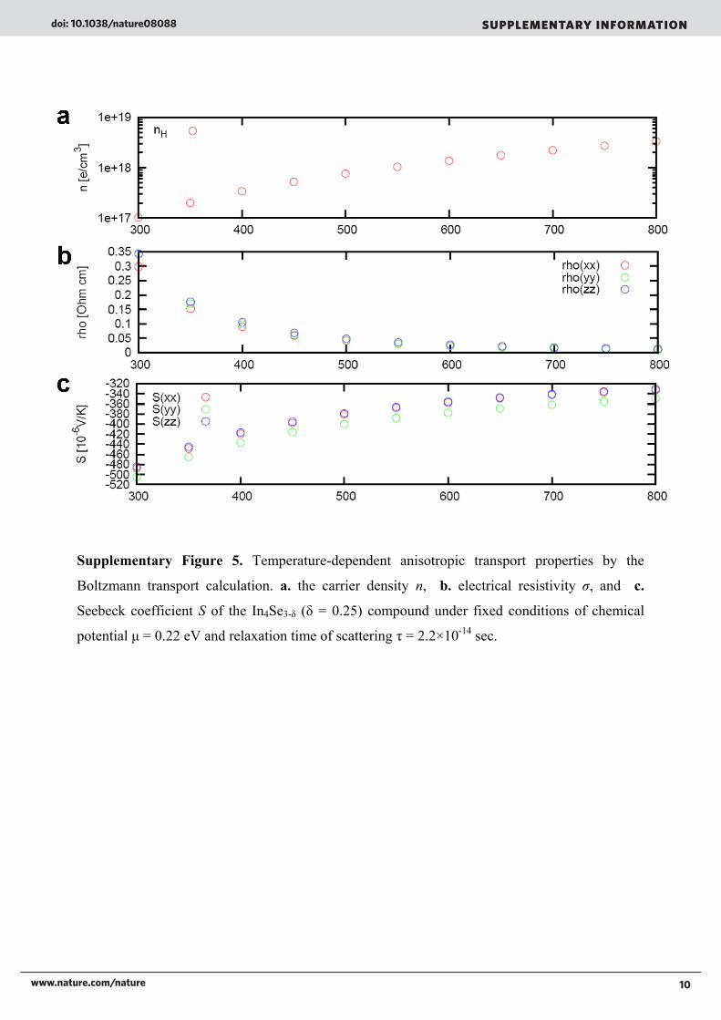
Suppl. Fig. 3 shows the thermoelectric properties of In4Se2.78 (δ = 0.22, black square) and
In4Se2.35 (δ = 0.65, red circle) for both orientations of the growth direction (ab-plane, open
symbol) and perpendicular to the growth direction (bc-plane, closed symbol). The thermal
conductivity κ(T) of In4Se3-δ is very low (1.5 W m-1 K-1 at 300 K) along the c-direction, and it
doi: 10.1038/nature08088 SUPPLEMENTARY INFORMATION
www.nature.com/nature 3
decreases with increasing the Se-deficiency: 0.94 W m-1 K-1 for δ = 0.22 and 0.74 W m-1 K-1 for
δ = 0.65 at T = 705 K, which is due to the disorders induced by the Se-defect. The low thermal
conductivity in the ab-plane for the δ = 0.65 crystal is caused by the van der Waals interaction
between the In-Se layers.
The Seebeck coefficient S(T) and electrical resistivity ρ(T) are presented in Suppl. Fig. 3b and
3c, respectively. The temperature-dependent behavior of S(T) for the δ = 0.22 crystal increases
with temperature up to 450 K and saturates at higher temperatures (~ - 310 μV/K), while the S(T)
for the δ = 0.65 crystal along the c-axis monotonically decreases with increasing temperature,
reaching ~ 295 μV/K at 705 K. The ρ(T) shows a gap-like increase with decreasing temperature
as shown in Suppl. Fig. 3c. At temperatures lower than 400 K, in the case of the δ = 0.65 crystal,
ρ(T) in the ab-plane is smaller than that measured in the bc-plane.
The power factor S2σ for these compounds, which is depicted in the inset of Suppl. Fig. 3c,
increases with temperature. The power factor reaches about 1.5 mW m-1 K-2 at 705 K for δ =
0.65 compound. The materials’ dimensionless figure of merit ZT is presented in Suppl. Fig.3d.
The value of ZT reaches remarkably high values of 1.48 and 1.10 for In4Se2.35 (δ = 0.65) and
In4Se2.78 (δ = 0.22), respectively, at 705 K along the bc-plane. The Hall carrier concentration nHall
of the In4Se2.78 (δ = 0.22) crystal in the ab-plane, which is determined by Hall resistivity
measurements, estimated to be 7×1018 cm-3, as shown in the inset of Suppl. Fig. 3d.
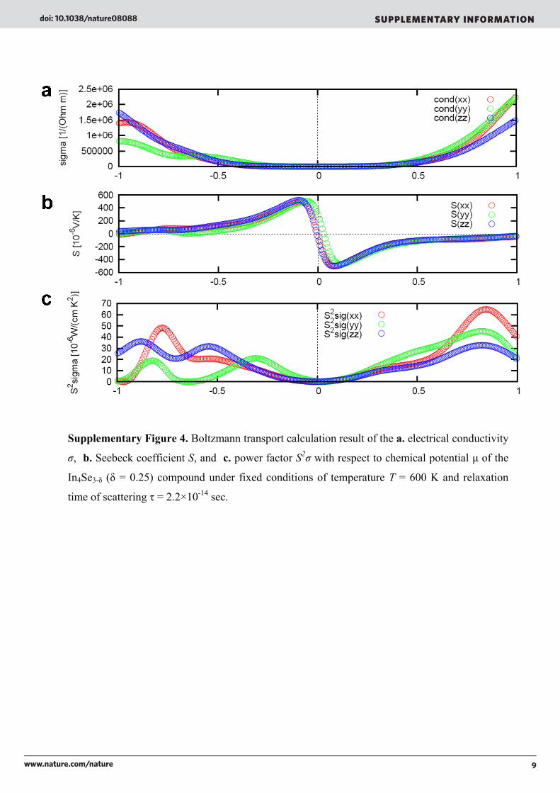
Boltzman transport calculation
Suppl. Fig. 4 represents the anisotropic Boltzman transport calculation results of electrical
conductivity σ, Seebeck coefficient S, and power factor S2σ with respect to chemical potential μ
of the In4Se3 compound. The positive (negative) chemical potential indicates the electron (hole)
doping, respectively. With increasing chemical potential by electron doping, the electrical
conductivity significantly increases at high chemical potential range (μ≥0.5 eV) and the absolute
Seebeck coefficient shows maximum at μ = 0.1 eV with saturation value of S at μ≥0.5 eV. The
power factor is maximum near μ = 0.8 eV due to significantly increase of the electrical
conductivity at high electron doping range. The Boltzman transport result as shown in Fig. 2 of
the main text used the chemical potential of μ=0.22 eV which is comparable to the experimental
properties. Because it is not an optimum value for high power factor, the power factor of the
doi: 10.1038/nature08088 SUPPLEMENTARY INFORMATION
www.nature.com/nature 4
presented compound In4Se3-δ (δ = 0.64, ZT = 1.48 at T = 705 K) can be further increased by
increasing electron doping (up to μ = 0.8 eV) level.
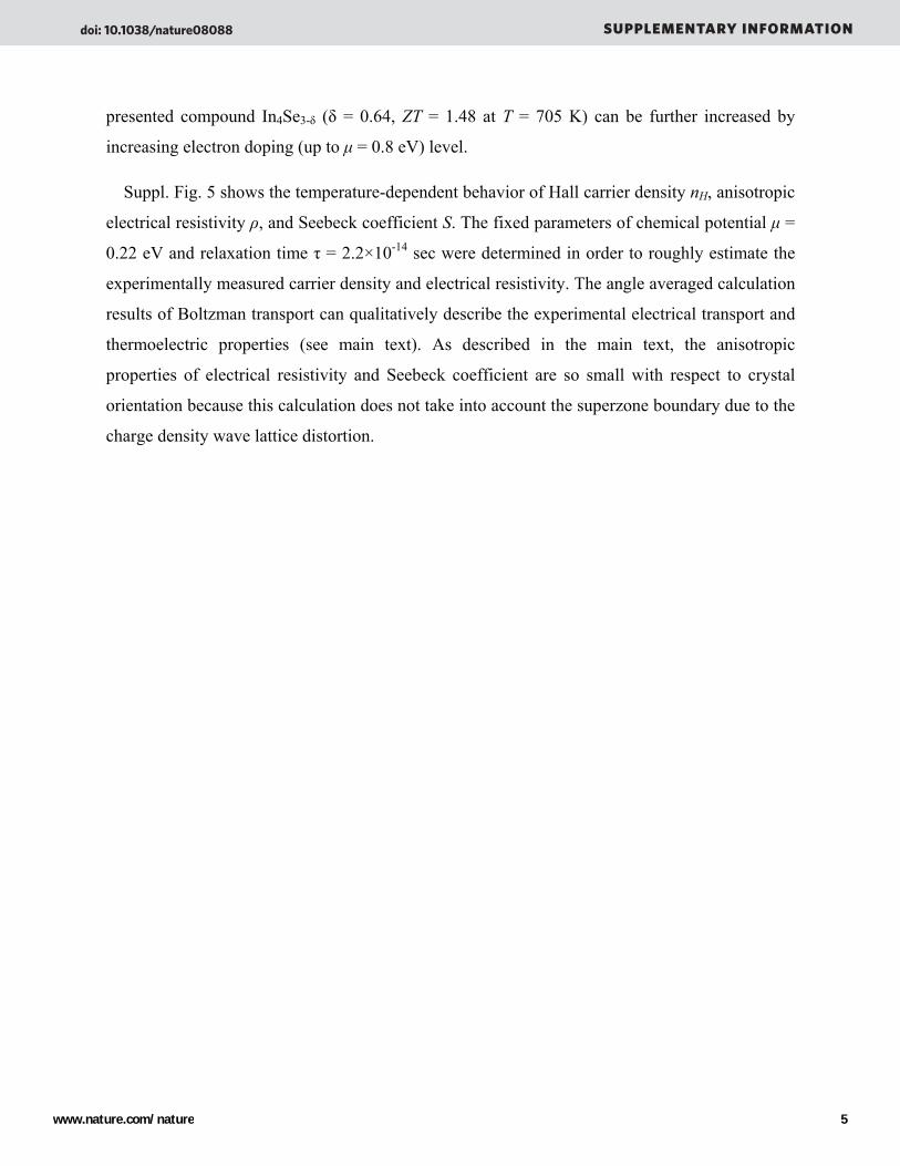
Suppl. Fig. 5 shows the temperature-dependent behavior of Hall carrier density nH, anisotropic
electrical resistivity ρ, and Seebeck coefficient S. The fixed parameters of chemical potential μ =
0.22 eV and relaxation time τ = 2.2×10⁻¹⁴ sec were determined in order to roughly estimate the
experimentally measured carrier density and electrical resistivity. The angle averaged calculation
results of Boltzman transport can qualitatively describe the experimental electrical transport and
thermoelectric properties (see main text). As described in the main text, the anisotropic
properties of electrical resistivity and Seebeck coefficient are so small with respect to crystal
orientation because this calculation does not take into account the superzone boundary due to the
charge density wave lattice distortion.
doi: 10.1038/nature08088 SUPPLEMENTARY INFORMATION
www.nature.com/nature 5

6www.nature.com/nature
doi: 10.1038/nature08088 SUPPLEMENTARY INFORMATION
Supplementary Figure 1. Binary phase diagram of In-Se. The starting compositions of grown
crystals of In4Se3-δ (δ = 0.65 and 0.22) are of In67Se33 and In63Se37, respectively. Excess In as
much as 4 at.% segregated at the top of the crystal ingots. Red horizontal line represents the
melting (590 oC) and crystallizing temperature (460 oC) range of δ = 0.22 compound.
Supplementary Figure 2. a. Crystal structure of In4Se3: Perspective view of the ab-plane.
Covalently bonded In-Se layers are stacked in the a-axis direction. Each covalently bonded layer
is bonded to neighboring layers by relatively strong van der Waals interaction. Extra In atoms
reside in the interstitial sites between the multivalent In-Se clusters. b. Side view of the bc-plane
of In4Se3 crystal. c. XRD pattern of the cross-sectional area of the crystal ingot, In4Se3-δ (δ =
0.22). d. In4Se3-δ (δ = 0.22) crystal ingot grown by the Bridgeman method. Crystallographic c-
axis is perpendicular to the growth direction. One grid spacing in the background is 5×5 mm2.
Supplementary Figure 3. Thermoelectric properties of Se-deficient In4Se3-δ crystals of (δ = 0.22
(black squares) and δ = 0.65 (red circles). Open and closed symbols indicate measurements in the
ab-plane and along the bc-plane, respectively. a. Temperature-dependent thermal conductivities
κ(T). b. Temperature-dependent Seebeck coefficient S(T). c. Temperaturedependent electrical
resistivity ρ(T) and power factor defined by S2σ (inset). d. Temperaturedependent dimensionless
figure-of-merit ZT and effective carrier concentration nHall (inset).
Supplementary Figure 4. Boltzmann transport calculation result of the a. electrical conductivity
σ, b. Seebeck coefficient S, and c. power factor S2σ with respect to chemical potential μ of the
In4Se3-δ (δ = 0.25) compound under fixed conditions of temperature T = 600 K and relaxation
time of scattering τ = 2.2×10⁻¹⁴ sec.

7www.nature.com/nature
SUPPLEMENTARY INFORMATIONdoi: 10.1038/nature08088
Supplementary Figure 1. Binary phase diagram of In-Se. The starting compositions of grown
crystals of In4Se3-δ (δ = 0.65 and 0.22) are of In67Se33 and In63Se37, respectively. Excess In as
much as 4 at.% segregated at the top of the crystal ingots. Red horizontal line represents the
melting (590 oC) and crystallizing temperature (460 oC) range of δ = 0.22 compound.
Supplementary Figure 2. a. Crystal structure of In4Se3: Perspective view of the ab-plane.
Covalently bonded In-Se layers are stacked in the a-axis direction. Each covalently bonded layer
is bonded to neighboring layers by relatively strong van der Waals interaction. Extra In atoms
reside in the interstitial sites between the multivalent In-Se clusters. b. Side view of the bc-plane
of In4Se3 crystal. c. XRD pattern of the cross-sectional area of the crystal ingot, In4Se3-δ (δ =
0.22). d. In4Se3-δ (δ = 0.22) crystal ingot grown by the Bridgeman method. Crystallographic c-
axis is perpendicular to the growth direction. One grid spacing in the background is 5×5 mm2.
Supplementary Figure 3. Thermoelectric properties of Se-deficient In4Se3-δ crystals of (δ = 0.22
(black squares) and δ = 0.65 (red circles). Open and closed symbols indicate measurements in the
ab-plane and along the bc-plane, respectively. a. Temperature-dependent thermal conductivities
κ(T). b. Temperature-dependent Seebeck coefficient S(T). c. Temperaturedependent electrical
resistivity ρ(T) and power factor defined by S2σ (inset). d. Temperaturedependent dimensionless
figure-of-merit ZT and effective carrier concentration nHall (inset).
Supplementary Figure 4. Boltzmann transport calculation result of the a. electrical conductivity
σ, b. Seebeck coefficient S, and c. power factor S2σ with respect to chemical potential μ of the
In4Se3-δ (δ = 0.25) compound under fixed conditions of temperature T = 600 K and relaxation
time of scattering τ = 2.2×10⁻¹⁴ sec.

8www.nature.com/nature
doi: 10.1038/nature08088 SUPPLEMENTARY INFORMATION
Supplementary Figure 1. Binary phase diagram of In-Se. The starting compositions of grown
crystals of In4Se3-δ (δ = 0.65 and 0.22) are of In67Se33 and In63Se37, respectively. Excess In as
much as 4 at.% segregated at the top of the crystal ingots. Red horizontal line represents the
melting (590 oC) and crystallizing temperature (460 oC) range of δ = 0.22 compound.
Supplementary Figure 2. a. Crystal structure of In4Se3: Perspective view of the ab-plane.
Covalently bonded In-Se layers are stacked in the a-axis direction. Each covalently bonded layer
is bonded to neighboring layers by relatively strong van der Waals interaction. Extra In atoms
reside in the interstitial sites between the multivalent In-Se clusters. b. Side view of the bc-plane
of In4Se3 crystal. c. XRD pattern of the cross-sectional area of the crystal ingot, In4Se3-δ (δ =
0.22). d. In4Se3-δ (δ = 0.22) crystal ingot grown by the Bridgeman method. Crystallographic c-
axis is perpendicular to the growth direction. One grid spacing in the background is 5×5 mm2.
Supplementary Figure 3. Thermoelectric properties of Se-deficient In4Se3-δ crystals of (δ = 0.22
(black squares) and δ = 0.65 (red circles). Open and closed symbols indicate measurements in the
ab-plane and along the bc-plane, respectively. a. Temperature-dependent thermal conductivities
κ(T). b. Temperature-dependent Seebeck coefficient S(T). c. Temperaturedependent electrical
resistivity ρ(T) and power factor defined by S2σ (inset). d. Temperaturedependent dimensionless
figure-of-merit ZT and effective carrier concentration nHall (inset).
Supplementary Figure 4. Boltzmann transport calculation result of the a. electrical conductivity
σ, b. Seebeck coefficient S, and c. power factor S2σ with respect to chemical potential μ of the
In4Se3-δ (δ = 0.25) compound under fixed conditions of temperature T = 600 K and relaxation
time of scattering τ = 2.2×10⁻¹⁴ sec.
9www.nature.com/nature
SUPPLEMENTARY INFORMATIONdoi: 10.1038/nature08088
Supplementary Figure 1. Binary phase diagram of In-Se. The starting compositions of grown
crystals of In4Se3-δ (δ = 0.65 and 0.22) are of In67Se33 and In63Se37, respectively. Excess In as
much as 4 at.% segregated at the top of the crystal ingots. Red horizontal line represents the
melting (590 oC) and crystallizing temperature (460 oC) range of δ = 0.22 compound.
Supplementary Figure 2. a. Crystal structure of In4Se3: Perspective view of the ab-plane.
Covalently bonded In-Se layers are stacked in the a-axis direction. Each covalently bonded layer
is bonded to neighboring layers by relatively strong van der Waals interaction. Extra In atoms
reside in the interstitial sites between the multivalent In-Se clusters. b. Side view of the bc-plane
of In4Se3 crystal. c. XRD pattern of the cross-sectional area of the crystal ingot, In4Se3-δ (δ =
0.22). d. In4Se3-δ (δ = 0.22) crystal ingot grown by the Bridgeman method. Crystallographic c-
axis is perpendicular to the growth direction. One grid spacing in the background is 5×5 mm2.
Supplementary Figure 3. Thermoelectric properties of Se-deficient In4Se3-δ crystals of (δ = 0.22
(black squares) and δ = 0.65 (red circles). Open and closed symbols indicate measurements in the
ab-plane and along the bc-plane, respectively. a. Temperature-dependent thermal conductivities
κ(T). b. Temperature-dependent Seebeck coefficient S(T). c. Temperaturedependent electrical
resistivity ρ(T) and power factor defined by S2σ (inset). d. Temperaturedependent dimensionless
figure-of-merit ZT and effective carrier concentration nHall (inset).
Supplementary Figure 4. Boltzmann transport calculation result of the a. electrical conductivity
σ, b. Seebeck coefficient S, and c. power factor S2σ with respect to chemical potential μ of the
In4Se3-δ (δ = 0.25) compound under fixed conditions of temperature T = 600 K and relaxation
time of scattering τ = 2.2×10⁻¹⁴ sec.
10www.nature.com/nature
doi: 10.1038/nature08088 SUPPLEMENTARY INFORMATION
Supplementary Figure 5. Temperature-dependent anisotropic transport properties by the
Boltzmann transport calculation. a. the carrier density n, b. electrical resistivity σ, and c.
Seebeck coefficient S of the In4Se3-δ (δ = 0.25) compound under fixed conditions of chemical
potential μ = 0.22 eV and relaxation time of scattering τ = 2.2×10⁻¹⁴ sec.