switching components for medium voltage drives … · switching components for medium voltage...
TRANSCRIPT

LAPPEENRANTA UNIVERSITY OF TECHNOLOGY
Faculty of Technology
Electrical Engineering
Alexey Mozalev
SWITCHING COMPONENTS FOR MEDIUM VOLTAGE DRIVES
Examiners: Professor Pertti Silventoinen
D.Sc. (Tech.) Juha-Pekka Ström

ABSTRACT
Lappeenranta University of Technology
Faculty of Technology
Degree in Electrical Engineering
Alexey Mozalev
Switching components for medium voltage drives
Master’s thesis
2011
75 pages, 28 figures, 26 tables, 2 appendices
Examiners: Professor Pertti Silventoinen,
D.Sc. (Tech.) Juha-Pekka Ström.
Keywords: motor drives, power semiconductor switches, insulated gate bipolar transistor, integrated
gate commutated thyristor, IGBT, IGCT.
Nowadays power drives are the essential part almost of all technological processes. Improvement of efficiency and reduction of losses require development of semiconductor switches. It has a particular meaning for the constantly growing market of renewable sources, especially for wind turbines, which demand more powerful semiconductor devices for control with growth of power. Also at pre-sent semiconductor switches are the key component in energy transmission, optimization of genera-tion and network connection.
The aim of this thesis is to make a survey of contemporary semiconductor components, showing dif-ference in structures, advantages, disadvantages and most suitable applications. There is topical in-formation about voltage, frequency and current limits of different switches. Study tries to compare dimensions and price of different components. Main manufacturers of semiconductor components are presented with the review of devices produced by them, and a conclusion about their availability was made.
IGBT is selected as a main component in this study, because nowadays it is the most attractive com-ponent for usage in power drives, especially at the low levels of medium voltage. History of devel-opment of IGBT structure, static and dynamic characteristics are considered. Thesis tells about as-semblies and connection of components and problems which can appear. One of key questions about semiconductor materials and their future development was considered. For the purpose of compari-son strong and weak sides of different switches, calculation of losses of IGBT and its basic competi-tor – IGCT is presented.
This master’s thesis makes an effort to answer the question if there are at present possibilities of ac-curate selection of switches for electrical drives of different rates of power and looks at future possi-ble ways of development of semiconductor market.

ACKNOWLEDGEMENTS
I am grateful to Professor Pertti Silventoinen for the help and useful advices during the way of writ-
ing of this master’s thesis. I value time which he spent on explanation of some obscure things for
me. Our meetings were always free and easy. Especially I appreciate his methods of work with me,
because I could choose the way and direction of thinking by myself.
I would like to express gratitude to D.Sc. (Tech.) Juha-Pekka Ström for his valuable advices which
helped me much to improve this study. I tried to follow all of them.
I am very grateful to all my family for the tireless support, help and care of me. It is very important
to feel it every time. As well I thank friends which were interested in my life and worried about me
in this year. I appreciate it very much!
I would like to thank Julia Vauterin for giving me great possibility to live and study in Finland in
this year.
Also I would like to thank all good people whom I have met and with whom I have been communi-
cated in Lappeenranta. All of them have influenced on my mind and opinion and maybe some of
them have improved me a little bit. Thank you for taking a part in making my stay in Lappeenranta
memorable.
Lappeenranta, May 2011
Alexey Mozalev

4
TABLE OF CONTENTS
List of symbols and abbreviations..................................................................................................... 7
1. Introduction................................................................................................................................... 10
1.1. Concept of medium voltage drives................................................................................. 12
1.2. Topologies of DC/AC converters................................................................................... 13
1.3. Demands to voltage level of applicable switches........................................................... 14
1.4. Target industries and applications of medium voltage drives........................................ 17
2. Medium voltage and high voltage controllable switching components........................................ 19
2.1. Thyristor (SCR).............................................................................................................. 19
2.2. Gate turn-off thyristor (GTO)......................................................................................... 20
2.3. Integrated gate-commutated thyristor (IGCT/ GCT)................................................... 21
2.4. Metal-oxide-semiconductor field effect transistor (MOSFET)...................................... 22
2.5. Insulated gate bipolar transistor (IGBT)......................................................................... 23
2.6. Comparison of power switches....................................................................................... 25
3. Semiconductor materials................................................................................................................ 29
3.1. Silicon (Si)...................................................................................................................... 29
3.2. Germanium (Ge)............................................................................................................. 29
3.3. Gallium arsenide (GaAs)................................................................................................ 29
3.4. Silicon carbide (SiC)....................................................................................................... 29
3.5. Gallium nitride (GaN)..................................................................................................... 30
4. Manufacturers................................................................................................................................ 32
4.1. ABB............................................................................................................................... 32
4.2. Infineon Technologies (Eupec)....................................................................................... 32
4.3. Semikron......................................................................................................................... 33
4.4. International rectifier...................................................................................................... 33
4.5. Dynex Semiconductor.................................................................................................... 33
4.6. Mitsubishi Electric.......................................................................................................... 34
4.7. Hitachi............................................................................................................................ 34
4.8. Toshiba............................................................................................................................ 34
4.9. Fuji Electric Systems...................................................................................................... 35
4.10. Ixys............................................................................................................................... 35

5
4.11. Powerex........................................................................................................................ 35
4.12. Fairchild Semiconductor.............................................................................................. 36
4.13. JSC «Electrovipryamitel»............................................................................................. 36
4.14. JSC «Proton–Electrotex»............................................................................................. 37
4.15. Resultant comparison of manufacturers....................................................................... 37
5. IGBT structure technologies.......................................................................................................... 40
5.1. Punch-through IGBT (PT-IGBT)................................................................................... 40
5.2. Non-punch-through IGBT (NPT-IGBT)........................................................................ 41
5.3. Soft-punch-through/ Light-punch-through IGBT (SPT/LPT-IGBT).............................. 42
5.4. Depletion stop/ Field stop trench IGBT......................................................................... 42
5.5. Injection enhanced gate transistor (IEGT)...................................................................... 43
5.6. Carrier stored trench bipolar transistor (CSTBT)........................................................... 43
6. Characteristics of IGBT................................................................................................................. 45
6.1. Static characteristics........................................................................................................ 45
6.2. Switching characteristics................................................................................................ 45
6.3. Gate resistance................................................................................................................ 46
6.4. Capacitance characteristics............................................................................................. 48
6.5. Safe operating areas (FBSOA, RBSOA, SCSOA)........................................................ 48
6.6. Internal diode (FWD) characteristics............................................................................. 49
6.7. Transient thermal resistance characteristics.................................................................... 50
7. Connection of IGBT...................................................................................................................... 52
7.1. Series connection of IGBT............................................................................................. 52
7.2. Parallel connection of IGBT........................................................................................... 52
7.3. Hybrid IGBT-IGCT switch............................................................................................. 54
8. Loss calculation............................................................................................................................. 57
8.1. IGBT loss calculation..................................................................................................... 57
8.2. IGCT loss calculation..................................................................................................... 58
8.3. Loss calculation analysis................................................................................................ 59
9. Future of power semiconductors................................................................................................... 61
9.1. Assemblies of IGBT....................................................................................................... 61
9.2. Perspectives of development of the semiconductor industry......................................... 62

6
10. Conclusions................................................................................................................................. 64
References......................................................................................................................................... 67
Appendices........................................................................................................................................ 74

7
LIST OF SYMBOLS AND ABBREVIATIONS
Abbreviations
ABB Swedish-Swiss-Finnish company in power and automation technologies;
AC Alternating current;
BJT Bipolar junction transistor;
CSI Current-source inverter;
CSTBT Carrier stored trench bipolar transistor;
DIAC Diode for alternating current;
DC Direct current;
DS Depletion stop;
FACTS Flexible alternating current system;
FS Field stop;
FWD Freewheeling diode;
GaAs Gallium arsenide;
Ge Germanium;
GTO Gate turn-off thyristor;
HV High voltage;
HVDC High voltage direct current;
HVIGBT High voltage insulated gate bipolar transistor;
IEGT Injection enhanced gate transistor;
IGBT Isolated gate bipolar transistor;
IGCT Integrated gate-commutated thyristor;
IPM Intelligent power module;
IR International rectifier – manufacturer of semiconductor devices;
JFET Junction gate field-effect transistor;
JSC Joint stock company;
LV Low voltage;
MOS Metal-oxide-semiconductor;
MOSFET Metal-oxide-semiconductor field effect transistor;
MV Medium voltage;
NPC Neutral-point-clamped;
8
PIN Diode with additional i layer between p and n layers;
PV Photovoltaic;
ROHS Restriction of hazardous substances directive;
RSOA Reverse bias safe operating area;
RUR Russian rouble;
SCR Silicon controlled rectifier;
Si Silicon;
SiC Silicon carbide;
SOA Safe operating area;
TRIAC Triode for alternating current;
UPM Finnish pulp and paper manufacturer;
VSI Voltage-source inverter;
ZSI Impedance-source inverter;
Symbols
CCE Collector-emitter capacitance;
CGC Gate-emitter capacitance;
CGE Gate-emitter capacitance;
CIES Gate-emitter input capacitance;
COES Collector-emitter output capacitance;
CRES Collector-gate reverse transfer capacitance;
EON Switching losses during the turn-on;
EOFF Switching losses during the turn-off;
ERR Reverse-recovery energy;
f Switching frequency;
I0 Average forward current;
IC DC collector current;
ID Continuous drain current;
IDRM Repetitive peak reverse current;
IF Continuous forward current;
IFAV Average (rectified) forward current;
IFAVM Maximum average (rectified) forward current;

9
IRRM Repetitive peak reverse current;
ITAV Average forward current;
ITAVM Maximum average forward current;
ITGQM Maximum controllable turn-off current;
ITQRM Repetitive controllable on state current;
QR Gate charge capacity;
rC Collector-emitter on-state resistance;
rD Diode resistance;
RTH Transient thermal resistance;
RTH(CH) Thermal resistance of contact between heat sink and case of the device;
RTH(HA) Thermal resistance of heat sink-ambient;
RTH(JC) Thermal resistance of junction-device case;
RG Gate resistivity;
tF Time in which collector current is reduced from 90% to 10% of maximum value;
TJ Junction temperature;
VBRDSS Drain to source breakdown voltage;
VCE Collector-emitter voltage;
VCE(SAT) Collector-emitter saturation voltage;
VCES Maximum permissible collector voltage;
VDRM Repetitive peak off-state voltage;
VDS Drain to source voltage;
VDSM Maximum surge peak forward blocking voltage;
VDSS Drain-source voltage;
VGE Gate-emitter voltage;
VGS(TH) Gate-source threshold value;
VR Reverse voltage;
VRRM Repetitive peak reverse voltage;
VRSM Maximum surge peak reverse blocking voltage;
ZTH Thermal resistance;
€ Euro (European currency).

10
1. INTRODUCTION
Nowadays power electronics is probably the most developed part of the market of equipment for
energy sector and in electrical engineering. The huge advance of power electronics for the last sev-
eral decades gives the possibility of right choice of semiconductor devices for specific usage, trying
to use best characteristics of each switch depending on technical demands and constraints. This
question is especially topical in the medium voltage range, where many semiconductor devices can
substitute for each other and in order to increase the efficiency and reduce costs the selection of
switches should be done as accurate as possible. More in details about voltage rates will be told in
section 1.1.
At present there is a goal to substitute hydrocarbon sources of energy by renewable sources as much
as possible. In future oil can be replaced by liquid gas and nuclear energetics with additional renew-
able sources, like wind energy, solar energy, energy of water and usage of biomass. In indetermi-
nate future thermonuclear power can change nuclear power, but nowadays there is not any deserving
results in this field. Power switches are key components in process of energy transmission, optimi-
zation of generation and network connection. Permanently growing number and power of mounted
wind turbines, PV panels and wide usage of power drives causes research of new structures and
semiconductor materials. In contemporary wind applications, requirements of quality of electricity
have to be implemented, so wind turbines should be connected to the grid without usage of addition-
al power electronics. The main aim of power electronics circuits is to keep output voltage and fre-
quency in specified level, independently of the current state of the wind turbine. As for solar cells,
development of semiconductor switches will improve efficiency of the whole solar energy sector.
Nowadays main problems in this field appear in solar inverters and lacks concern quite low efficien-
cy, harmonics and electromagnetic interference caused due the usage of long length connecting ca-
bles.
The aim of this master’s thesis is to make a survey of contemporary semiconductor components
which can be used in power drives with emphasis on IGBT. IGBT is chosen as a basis of this study,
because at present this device shows the most probable potential of development and usage in elec-
trical drives. History of IGBT structure development, features and main characteristics are present-
ed. This thesis analysis up-to-date semiconductor switches, presents advantages, disadvantages, ap-

11
plication of different devices and their availability and tries to present the price on some devices.
Work contains topical information about main players of semiconductor market and today’s voltage
and current limits of produced devices.
One of the most interesting questions is to compare devices in different states. This shows applica-
bility of components. Calculation of losses was made with aim to compare an order of losses and
understand strong and weak sides of components.
Contemporary semiconductor switches are generally components of DC/AC converters. One of
basic questions is a right choice of switches for specific topology of the frequency converters. With
this purpose the question of selection of appropriate switches for certain voltage levels is considered.
This study can be quite important in a great number of published surveys devoted to semiconductor
components. The main reason is in fact that most of them were made in the last years of previous
century and in first years of XXI century. It can be explained by the creation of IGCT approximately
in 1996. This device made engineers to compare studiously it with IGBT and with previous types of
thyristors. Nowadays plenty of companies produce IGBT and only few of them manufacture IGCT,
therefore qualitative surveys and analyses last years were made only by manufacturers who present
both IGBT and IGCT. One more advantage of this work is in fact that it contains good results and
strong sides of surveys of previous years and also based on up-to-date numbers and information.
Thesis tries to ask the question about potential of development of semiconductor market and devel-
opment of semiconductor materials, structures and assemblies in particular.

12
1.1. Concept of medium voltage drives
Figure 1 Simplified working schemes of electrical drive. [29]
The concept of electrical drive comprises power electronics, electrical motor, controller, measuring
equipment and external parameters. Figure 1 depicts simplified general idea of electrical drive. It
should be noticed that in some simple applications can be used drive with rectifier- Figure 1a, but it
is often necessary to return energy into the ac main or dissipate it in the intermediate circuit of fre-
quency converter. For example this necessity can appear during the electromagnetic braking, while
machine starts to act as a generator and rotating speed exceeds the synchronous speed, therefore slip
becomes negative and motor reduces the speed. This can be implemented by usage of inverter in-
stead of rectifier, because normally rectifier bridge can not be reversed. [1], [30]
Most of contemporary applications of drives are in the medium voltage range, therefore it is a wide
field of usage of medium voltage and high voltage semiconductor components. The definition of
medium voltage is depended on industry and application. For AC motors it varies from 1 kV to 15
kV. The European threshold of MV is 1 kV. Existing medium voltage drives have range from 2.3
kV to 7.2 kV. In North America 2.3 kV and 4.16 kV (60 Hz) are referred to the medium voltage
range, while prevalent line voltages in Europe and in other parts of the world are 3.3 kV and 6.6 kV
(50 Hz). Figure 2 shows average ratings of voltage and power of the concept of MV drives.
Figure 2 a) Voltage range, b) Power range of medium voltage drives. [29]

13
Further this study will not differentiate medium voltage and high voltage ranges of switching devic-
es, because this border is quite smooth.
1.2. Topologies of DC/AC converters
DC/AC converter is the essential part of electrical drive. Semiconductor components form basis of
converters. It is a widely developed field of power electronics. Traditionally there are two types of
converters: voltage-source inverters (VSI) and current-source inverters (CSI). Quite recently imped-
ance-source inverter (ZSI) was invented. Simplified schemes of these devices are depicted on the
Figure 3.
Figure 3 a) Current-source inverter, b) Voltage-source inverter, c) Impedance-source inverter. [29], [41]
The main difference between VSI and CSI is that in first device DC link has not impedance in ideal
way, but in second device there is impedance approaching to infinity in ideal case. As opposed to
VSI and CSI, ZSI uses the shoot through switching state which means that switching components,
which connected to the same leg, can be switched-on at the same period. Z-source can be seen on
the Figure 3c. Owing to it, the short through state which causes short circuit in traditional schemes is
not harmful in this modification of an inverter. [1], [41]
14
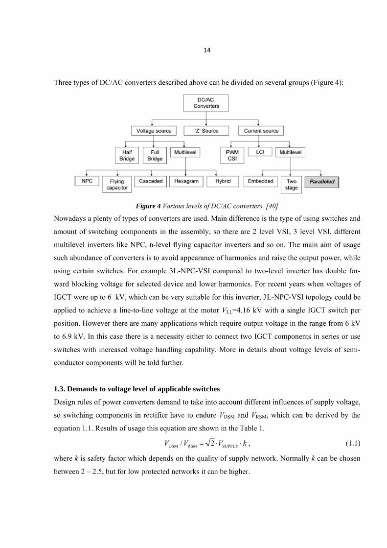
Three types of DC/AC converters described above can be divided on several groups (Figure 4):
Figure 4 Various levels of DC/AC converters. [40]
Nowadays a plenty of types of converters are used. Main difference is the type of using switches and
amount of switching components in the assembly, so there are 2 level VSI, 3 level VSI, different
multilevel inverters like NPC, n-level flying capacitor inverters and so on. The main aim of usage
such abundance of converters is to avoid appearance of harmonics and raise the output power, while
using certain switches. For example 3L-NPC-VSI compared to two-level inverter has double for-
ward blocking voltage for selected device and lower harmonics. For recent years when voltages of
IGCT were up to 6 kV, which can be very suitable for this inverter, 3L-NPC-VSI topology could be
applied to achieve a line-to-line voltage at the motor VLL=4.16 kV with a single IGCT switch per
position. However there are many applications which require output voltage in the range from 6 kV
to 6.9 kV. In this case there is a necessity either to connect two IGCT components in series or use
switches with increased voltage handling capability. More in details about voltage levels of semi-
conductor components will be told further.
1.3. Demands to voltage level of applicable switches
Design rules of power converters demand to take into account different influences of supply voltage,
so switching components in rectifier have to endure VDSM and VRSM, which can be derived by the
equation 1.1. Results of usage this equation are shown in the Table 1.
DSM RSM SUPPLY/ 2V V V k , (1.1)
where k is safety factor which depends on the quality of supply network. Normally k can be chosen
between 2 – 2.5, but for low protected networks it can be higher.

15
Table 1 Recommended blocking voltages for chosen devices at nominal line voltages with k≈2.5. [42]
Nominal line voltage (VSUPPLY), VRMS Optimum blocking voltage ratings (VDSM, VDRM), V
400 1400
500 1800
690 2400
800 2800
1000 3600
1250 4200
1500 5200
1800 6500
Figure 5 illustrates simple difference between different voltages which influence on the choice of
semiconductor components. Misunderstanding of these features can lead to wrong choice of switch
and possible failure of equipment.
Figure 5 Definition of different voltages. [42]
Generally the selection of semiconductor switches for inverters may be based on equation 1.2, but of
course these calculations directly depend on the topology of the inverter. In case of inverter line to
line voltage fluctuations and voltage spikes during switch-off due stray inductances of the line are
taken into account. Approximate results of equation 1.2 are illustrated in the Table 2 and Table 3.
CE_MAX DC_NOM1.5...2.0V V , (1.2)

16
Table 2 Required blocking voltage in 3-level VSI. [53]
Nominal
line volt-
age,
V
Nominal
DC link
voltage,
V
Maximum DC
link voltage,
(25% over-
voltage)
V
Required semi-
conductor block-
ing voltage,
V
Number of series
connected devices.
VDRM=3300-5500 V
(number of devices
per phase)
Number of series
connected devices.
VDRM=3300-9500 V
(number of devices
per phase)
2300 1800 2250 3300 1(4) 1(4)
3300 2460 3100 4500 1(4) 1(4)
4160 3100 3900 5500 1(4) 1(4)
6000 4500 5600 8000 2(8) 1(4)
6600 4900 6200 9000 2(8) 1(4)
6900 5160 6500 9200 2(8) 1(4)
(7200) 5400 6750 9500 2(8) 1(4)
Table 3 Required blocking voltage in 3-level CSI. [53]
Nominal
line volt-
age,
V
Nominal
peak line-
to-line volt-
age,
V
Maximum
peak line-to-
line voltage,
V
Required semi-
conductor block-
ing voltage,
V
Number of series
connected devices.
VDRM=6500 V
(number of devices
per phase)
Number of series
connected devices.
VDRM=3300-9500 V
(number of devices
per phase)
2300 3394 3734 6500 1(2) 1(2)
3300 4667 5134 9000 2(4) 1(2)
4160 5883 6471 11500 2(4) 2(4)
6000 8485 9334 16500 3(6) 2(4)
6600 9334 10267 18000 3(6) 2(4)
6900 9758 10734 19000 3(6) 2(4)
(7200) 10182 11202 20000 3(6) 2(4)

17
According to principles described above, the 6.5 kV IGBT module can be chosen for 3.0 kVDC trac-
tion applications. Another important field of application is high power industrial drives with 2.3
kVAC lines (or 3.25 kVDC). In these applications converter can be connected to lines directly. Drives
with 4.16 kVAC (or 5.9 kVDC) can be implemented in three level circuit designs, however if to con-
cern 6 kV motors, in recent years they were operated by multilevel drives or LV drives in arrange-
ment with a transformer, which sometimes can’t be so suitable as usage of MV drives. Much energy
savings can be achieved in drives with more than 6.5 kV motor voltages. Expected cost reduction
can be implemented by increasing of the blocking voltage of semiconductor devices to 9.5 kV. Ow-
ing to 9.5 kV device it will be possible to make 3-level VSI and CSI without series connection of
switches. It will be told more in details about perspectives of development of power semiconductor
components in section 9. [42], [44], [53]
As power electronics is developed, the implementation and reliability of DC/AC converters is in-
creased, because the necessity to make converters consisting of large amount of switches is disap-
pear.
1.4. Target industries and applications of medium voltage drives
Power drives nowadays are the essential part of every industrial process and in many everyday and
domestic processes. Drives adapt speed of motor to the necessary need and thereby optimizing ener-
gy consumption and reducing emission of greenhouse gases. As was told in previous chapter, some-
times low-voltage drives with transformer are used to achieve higher power and LV drives have
lower size, but in spite of this MV drives have many advantages over LV drives. Medium-voltage
drives operate at much higher supply voltages, therefore at less currents. It reduces losses and length
of used cables, which prevent high voltage drop in the cable between drive and motor. Construction
of MV cable is more expensive, as a sequence of insulation demands, but amount of copper is less.
Other advantages in harmonic mitigation as opposed to LV drives and suitable synchronization with
network, because mains are usually MV. [64]
At present medium-voltage drives are used almost in all fields of industry. For example, Finland has
strong positions in the field of pulp and paper production. One of the pulp and paper factories which

18
belongs to UPM is situated in Lappeenranta. Such factories can operate during twenty-four hours,
therefore contemporary power drives are demanded to be reliable and robust.
Main applications are presented in the Table 4.
Table 4 Main applications of medium voltage drives. [14], [29]
Petrochemical Pipeline pumps, Gas compressors, Brine pumps, Mixers/ extruders, Electrical submersible pumps, Induced draft Fans, Boiler feed water pumps.
Forest Products Fan pumps, Induced draft fans, Boiler feed water pumps, Pulpers, Refiners, Kiln drivers, Line shafts.
Mining and Metals Slurry pumps, Ventilation fans, De-scaling pumps, Conveyors, Baghouse fans, Cyclone feed fans,
Cement Kiln induced draft fans, Forced draft fans, Cooler baghouse fans, Preheat tower fans, Raw mill induced draft fans, Kiln gas fans, Cooler exhaust fans, Separator fans, Baghouse fans.
Water/ Waste Water Raw sewage pumps, Bio-roughing tower pumps, Treatment pumps, Freshwater pumps, Water extraction.
Electrical power Feed water pumps, Induced draft pumps, Forced draft fans, Baghouse fans, Effluent pumps, Compressors, Wind turbines.
Marine Chemical, product, shuttle tankers, Cruise vessels, Double-acting tankers, Dredgers, Drill ships and semi-submersible rigs, FPSO tankers, Icebreakers, Offshore support vessels, Research and survey vessels, RoRo and RoPax ferries.
Miscellaneous Test stands, Wind tunnels, Agitators, Rubber mixers, Food and beverage, Elevators, Cranes, Escalators, Household appliances.
19
2. MEDIUM VOLTAGE AND HIGH VOLTAGE CONTROLLABLE SWITCHING
COMPONENTS
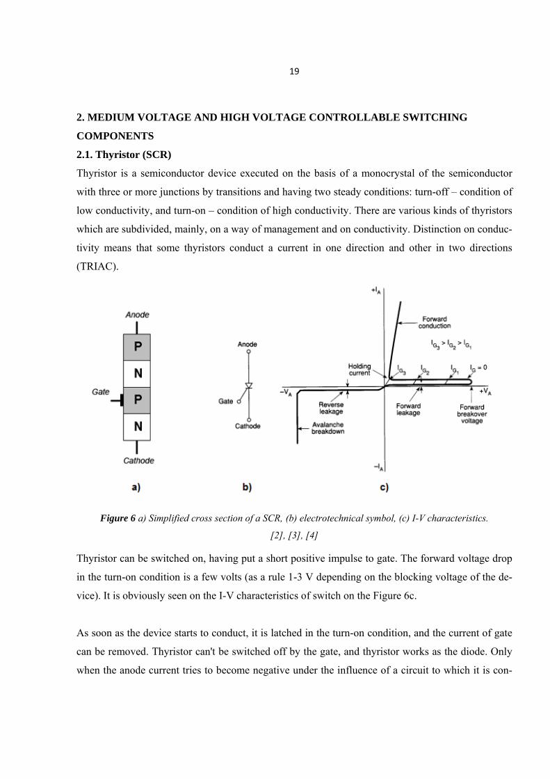
2.1. Thyristor (SCR)
Thyristor is a semiconductor device executed on the basis of a monocrystal of the semiconductor
with three or more junctions by transitions and having two steady conditions: turn-off – condition of
low conductivity, and turn-on – condition of high conductivity. There are various kinds of thyristors
which are subdivided, mainly, on a way of management and on conductivity. Distinction on conduc-
tivity means that some thyristors conduct a current in one direction and other in two directions
(TRIAC).
Figure 6 a) Simplified cross section of a SCR, (b) electrotechnical symbol, (c) I-V characteristics.
[2], [3], [4]
Thyristor can be switched on, having put a short positive impulse to gate. The forward voltage drop
in the turn-on condition is a few volts (as a rule 1-3 V depending on the blocking voltage of the de-
vice). It is obviously seen on the I-V characteristics of switch on the Figure 6c.
As soon as the device starts to conduct, it is latched in the turn-on condition, and the current of gate
can be removed. Thyristor can't be switched off by the gate, and thyristor works as the diode. Only
when the anode current tries to become negative under the influence of a circuit to which it is con-

20
nected, thyristor is switched off, and the current goes to zero. It allows gate to regain control switch
on the device in some controllable time after it has again entered the forward blocking condition.
In reverse bias voltages, only small electric current of leak flows in the thyristor. Forward- and re-
verse- blocking voltages of the thyristor are usually the same. [1]
2.2. Gate turn-off thyristor (GTO)
GTO is a device oriented to be used in high power applications. Device has four states: turn-on,
conducting state, turn-off and latching. GTO can be switched on by a short impulse of a gate cur-
rent, and being in turn-on condition GTO can remain in the on-state without a gate current. Howev-
er, unlike the thyristor, GTO can be switched off, putting negative gate-cathode voltage, thereby
causing enough big negative current through the gate. This negative gate current amplitude depends
on the anode current which should be switched off. Turn-off is provided by bypassing carriers di-
rectly to the gate circuit, its turn-off time is short, thus giving it more capability for high frequency
operation than thyristors. Simplified structure is shown in the Figure 7a and it illustrates difference
with structure of SCR (Figure 6a).
Figure 7 GTO: a) Simplified cross section of a GTO, (b) Electrotechnical symbol, (b) I-V characteristics. [1]
Thus it is not necessary to apply reverse biased anode voltage to achieve turn-off, so expensive
commutation circuits, which were used in association with SCR, are not required. Owing to it, turn-
ing off is much faster.

21
Snubber circuits are obligatory for GTO operation. Parallel connected capacitors limit du
dt during
turn-off and series connected coils limit di
dt during turn-on. They increase weight and size and de-
crease cost efficiency. Sometimes snubbers require additional cooling system. [1], [2], [5]
2.3. Integrated gate-commutated thyristor (IGCT/ GCT)
IGCT has very similar principle as GTO, but fast turn-off is implemented by transformation of thy-
ristor structure into transistor structure while latching, which makes a switch insensitive to du
dt.
Turn-on and turn-off states are achieved by applying a gate signal. Gate driver system of IGCT has
very low inductance and general difference in operation with GTO is in turn-off. As against to GTO,
IGCT has lower conduction losses and higher overvoltage capability.
IGCT has almost the same structure as GTO. In an IGCT, the gate turn off current is greater than the
anode current. This fact follows to stop the ejection of minority current carriers from the lower PN
junction, which leads to the faster turn-off. The main differences from the GTO are the lower size of
the cell and presence of gate drive in the body of IGCT. The integration of drive circuit into the
frame of device causes reduction of resistance and inductance of the connection.
Turn-off times of IGCT are much faster in comparison to GTO's. That allows them to work at higher
frequencies – up to several of kHz (more in details in Table 6). But higher losses appear on higher
frequencies. Operating frequency for IGCT is limited only by thermal conditions of the device, but
typically it is about 500 Hz.
Available several types of IGCT: asymmetric (IGCT), symmetric or reverse blocking (RB) and re-
verse conducting (RC). [7], [9]

22
Figure 8 Typical structures of IGCT. a) IGCT, b) RB-IGCT, c) RC-IGCT. [56]
Figure 6 illustrates difference in behavior of IGCT depending on the structure of the device.
2.4. Metal-oxide-semiconductor field effect transistor (MOSFET)
MOSFET is a type of JFET with input gate electrically insulated from the main current channel and
owing to it MOSFET works as a voltage controlled nonlinear resistor and the current flowing from
the drain to source through the main channel. This current is proportional to the input voltage. As a
JFET, MOSFET has very high input resistance, because of the isolated input gate. MOSFET is a
voltage controlled device. It is fully in the on-state and approaches a closed switch when the gate-
source voltage is below the threshold value VGS(TH). MOSFET requires the continuous application of
gate-source voltage of appropriate magnitude in order to be in the on-state. The switching times are
very short, being in the range of a few tens of nanoseconds to a few hundred nanoseconds depending
on the device type. MOSFET can be P-type and N-type.
Structure of MOSFET contains parasitic diode, which can be useful as a clamp diode during a
switching over an inductive load. Parasitic diode adds additional recovery losses. Simplified struc-
ture of MOSFET is illustrated on the Figure 9a and Figure 9c shows main I-V characteristics of the
switch. [1], [63]

23
Figure 9 A MOSFET: a) Simplified cross section of a n-type MOSFET (b) Electrotechnical symbol, (c) I-V
characteristics. [1], [3]
2.5. Insulated gate bipolar transistor (IGBT)
Insulated gate bipolar transistor consists of bipolar junction transistor which is operated by metal-
oxide-semiconductor field effect transistor, which can be seen in the simplified structure of IGBT on
the Figure 10a. Also it depicts difference with MOSFET structure (Figure 9a).
Figure 10 An IGBT: a) Simplified cross section of an IGBT cell, (b) Electrotechnical symbols, (c) I-V charac-
teristics. [1], [3], [4]
The IGBT has some advantages of the MOSFET, BJT and GTO combined. IGBT has high imped-
ance gate which is an advantage of the MOSFET. Owing to it only a small amount of energy re-
quires to switch the device. Similar to GTO, the IGBT can be designed to block negative voltages.
IGBT has high conduction current density and low voltage drop in the on-state. It is easy operated,

24
because of the MOS gate structure, as compared with current controlled switches. IGBT has wider
Safe Operating Area than BJT.
As against MOSFET, IGBT has less switching speed, but it has superior switching speed against
BJT. The current tail, because of the minority carriers, causes reduction of turn-off speed. Structure
of the IGBT contains a parasitic thyristor, so it can be latched.
IGBT and MOSFET occupy a range of average capacities and frequencies, partially replacing each
other. Generally, for high-frequency and low-voltage cascades, less than 1000 V most applicable is
MOSFET, and the most appropriate switch for voltage rate more than 1000 V is powerful IGBT.
Application of IGBT modules in control systems of traction engines allows (in comparison with thy-
ristor devices) to provide high efficiency, high smoothness of an operation of the machine and pos-
sibility of application of regenerative braking almost at any speed. IGBT is applied in devices with
voltage rate more than 1000 V, quite high temperature (more than 100 °C) and output power more
than 5 kW. The basic applications of IGBT are inverters, pulse regulators of the current and fre-
quency-regulated drives.
In certain cases IGBT and MOSFET – are completely interchangeable. The characteristic of operat-
ing signals of both devices – are identical. IGBT and MOSFET demand 12-15 V for switching-on.
[1], [36].
Table 5 Comparison of characteristics of IGBT, MOSFET and BJT. [36]
Features\ Device BJT MOSFET IGBT
Drive Method Current Voltage Voltage (charge)
Drive Circuit Complex Simple Simple
Input Impedance Low High High
Drive Power High Low Low
Switching Speed Slow (μs) Fast (ns) Middle
Operating Frequency Low (less than 100kHz) Fast (less than 1MHz) Middle
SOA Narrow Wide Wide
Saturation Voltage Low High Low

25
Table 5 shows comparison of advantages and disadvantages of IGBT, MOSFET and BJT which was
made by engineers of Fairchild Semiconductor Corporation.
Traditionally in literature IGBT is described as a voltage controlled device, but in practice it would
be incorrect. It is justice to tell that IGBT is controlled by voltage – current combination, namely by
a charge. This statement is relied on the gate charge which is proportional to the continuous current
rating of the IGBT and required gate current. Process of gate charge is impulsive and at high fre-
quencies high-voltage IGBT requires very high current for gate charge.
Structure and characteristics of IGBT will be discussed more in details further in section 5-6.
2.6. Comparison of power switches
The fully controlled GTO was traditionally used in high power systems, because of its off-state volt-
age capability and on-state current capability. IGBT was very popular in medium power applications
and the lower part of high power, especially when voltage is less than 1.5 kV. With appearance of
HVIGBT, IGBT is presented a challenge to predominance of the GTO in high power area. Switch-
ing performance of IGBT technology is much better than GTO’s, but switching performance of
GTO can be significantly improved by driving the gate current to be greater than or equal to the an-
ode current during turn-off. Thus the IGCT appeared. Another important characteristic of the GTO
and the IGCT is that they allow only on and off states. These switches are latching devices, while
IGBT can always be controlled in the whole range from off to on.
MOSFETs are usually used when there is necessity in very high switching frequency, but these
switches are applicable only for relatively low power applications. These devices are not applicable
in high power circuits. [12], [13]
Main advantages, disadvantages, voltage and frequency limits of the described above semiconductor
switches are presented in the Table 6. Table contains survey of semiconductor components which
are presented on the commercial market at present.

26
Table 6 Comparison of the semiconductor switches. [5] – [11]
Type of
the de-
vice
Advantages Disadvantages Voltage rate
(VDRM, VCES,
VDSS),
kV
Switching
frequency
range, kHz
Range of application
Thyristor Lowest losses in
the turn-on state.
The highest over-
load capacity in
comparison to oth-
er switches. High
reliability.
It is not capable for
compulsory latch-
ing on an operating
electrode.
≤12 traditional-
lyf≈0.05,
fast thyris-
tors have
f<10
DC drives, power
suppliers, equipment
for welding, melting
and heating, static
var compensators,
HVDC, AC switches.
GTO Controlled turn-off
ability. Relatively
high overload ca-
pacity. The relia-
bility and cost ef-
fectiveness.
High switching, on-
state loss, very high
loss in the control
system. Difficult
and expensive turn-
off snubbers. High
switching losses.
Slow switching:
10- 30 µs.
≤6.5 0.1 – 0.5 Adjustable speed
drives, static var
compensators,
HVDC, uninterrupti-
ble power supply
(UPS), equipment for
inductive heating.
IGCT Controlled turn-off
ability. Relatively
high overload ca-
pacity. Low losses
in the turn-on state
during the switch-
ing. Snubberless
turn-off.
IGCT needs addi-
tional circuits with
inductivity for re-
duction of di
dt.
≤6.5 Typical f
≈0.5,
upper f< 40
(limited
only by
thermal
conditions
of the de-
vice).
Power supplies, in-
verters, converters,
HVDC, power
drives.

27
MOSFET High working fre-
quency.
Low power of de-
vices.
≤1.5 <1000 Switch Mode Power
Supplies (SMPS),
uninterruptable pow-
er supplies (UPS),
inverters and DC mo-
tor drives.
IGBT Controlled turn-off
ability. Simple
control system with
integrated driver.
Current tail during
the switch-off, high
on-state losses.
≤6.5 ≤150 Power drives, unin-
terruptible power
supply (UPS), static
var compensators,
HVDC, active filters.
At present in consequence of very rapid development of IGBT it has probably the best characteris-
tics for usage in power drives in medium voltage ratings. It concerns to devices of the same power,
because in high voltage segment thyristor group is more applicable.
Nowadays only IGCT may be a competitor in medium voltage range. One of the advantages of
IGCT over IGBT is fewer amounts of components to achieve rated voltages, than the amount of IG-
BTs components. This way old generations of IGBT usually contained great number of chips and
connecting wires, while IGCT includes only several parts. Situation has changed with coming of
modules and IPM.
Latching behaviour of the IGCT during the on-state means that there is not essential limitation of
possible short circuit current. In addition, FWD can not be turned off with high di
dt,
which can appear. Therefore DC link contains additional inductivity which limits current spikes and
thereby protects FWD. Figure 11 depicts difference in operating of IGCT and IGBT on the example
of VSI. On the contrary IGBT in which current of internal transistor structure saturates in the on-
state. This allows IGBT to safely switch-off after detection of short circuit. Short circuit turn-off ca-
pability of IGBT is an additional advantage to slight MOS control. Parallel connection ability, ow-
ing to positive temperature coefficient of VCE(SAT), eases the operation of powerful modules without
huge failures. [28], [56]

28
Figure 11 Comparison of simplified circuits for the operation of a) IGCT, b) IGBT. [54]
Nowadays all equipment has to be as small as possible and development of components of higher
ratings reduces total dimensions of equipment and as result areas occupied by applications. Appen-
dices 1, 2 illustrate sizes of 6.5 kV IGBT and 6.5 kV IGCT. This pictures were taken from
datasheets of selected switches and it is obvious from them that IGBT has lower dimensions. This
comparison can be correct and for switches of other voltage ranges.
One of the most important factors is price. This factor usually makes the choice of the device. At
present it is almost impossible to get price list on high power components in a free access exactly
from manufacturers, because of the competition between them. Attempt of analysis of price of dif-
ferent devices was made according to information presented by Russian shop “Chip & Dip” (Saint
Petersburg) specializing in electronic components, therefore results are not very accurate. For com-
parison all prices were led to euro. Average ratio for April 2011 is 1 €=40 RUR. Price is retail for
single switch. Results are presented in the Table 7.
Table 7 Comparison of prices on different semiconductor switches. [54]
Shop\ Price on the device Thyristor GTO IGCT MOSFET IGBT
Chip & Dip (Saint Pe-
tersburg, Russia)
URRM=2000 V,
ITAV=230 A,
Vishay/ IR
Price=184.85 €
___* ___*
N-type MOSFET
VDS=1500 V,
ID=2.5 A,
Hitachi
Price=7.5 €
Single switch with
antiparallel diode
VCES=6500 V,
IC=200 A,
Mitsubishi,
Price≈1500 €
* Shop doesn’t sell this device
Unfortunately according to Table 7, a detailed conclusion about prices can not be made, but price on
the IGBT inverter which contains six switches will be at least 6 1500 9000 €.

29
3. SEMICONDUCTOR MATERIALS
3.1. Silicon (Si)
Silicon is the second most widely diffused element in the Earth’s crust after oxygen. Silicon is a
fundamental element in the most of semiconductor devices. Purity of silicon has great influence on
its electrical and physical characteristics and consequently on characteristics of the produced semi-
conductor component. Hyperpure silicon is mostly used for production of single modules of nonlin-
ear semiconductor devices. It is the primary product for the photovoltaic elements.
3.2. Germanium (Ge)
Germanium is applied for production of transistors and diodes. Ge has characteristics which are dif-
ferent from Si, in view of smaller unlocking voltages of PN-junction of Ge – 0.4 V against 0.6 V of
Si devices. Besides, back currents of Ge devices on some orders are more than those at Si. Germani-
um is applicable only in production of low power devices.
3.3. Gallium arsenide (GaAs)
Some electronic properties of GaAs exceed properties of Si. Gallium arsenide possesses higher mo-
bility of electrons which allows devices to work on frequencies to 250 GHz. Semiconductor devices
on the basis of GaAs generate less noise, than silicon devices on the same frequency. Because of
more high tension of electric field of breakdown in GaAs in comparison with Si, devices from galli-
um arsenide can work at higher power.
3.4. Silicon Carbide (SiC)
SiC has almost 170 polytypes and each of them has own physical characteristics. The best known
are 3C-SiC, 4H-SiC and 6H-SiC. Only last two compounds are commercially available. Nowadays
Silicon Carbide is one of the most promising semiconductor materials for manufacturing of power
components. It has many favourable characteristics for high temperature, high frequency and high-
power applications. In opposite to switches based on GaAs and Si, devices on SiC have following
advantages:
Band gap is several times wider than of GaAs;
Field strength of electrical breakdown is ten times bigger than of Si ;
High admissible working temperatures (to 600° C);

30
Heat conductivity is three times more over Si and almost ten times more over GaAs;
High-saturated drift velocity (higher than GaAs);
Stability at radiation influence;
Stability of electrical characteristics while temperature is changing;
Silicon Carbide has already been used in production of fast Schottky diodes, PIN diodes, zero re-
covery rectifiers, field effect transistors, MOSFETs and high-temperature thyristors.
In comparison to Si, SiC is more expensive and quite difficult to be manufactured, so for present Si
has much better positions on the semiconductor market.
3.5. Gallium nitride (GaN)
GaN has even better physical parameters than SiC, specifically the excellent transport properties and
low sensitivity ionizing radiation, which makes this material suitable for using in PV panels. It has
the biggest success in optoelectronics, owing to its wide band gap which is 3.39 eV. In comparison
to GaAs, GaN can work at higher temperatures and at much higher voltages. GaN is used for manu-
facturing of MOSFETS.
Table 8 Comparison of general properties of semiconductor materials. [39], [58], [59]
Characteristics\ Material Si Ge GaAs 3C-SiC 4H-SiC6H-
SiC GaN Diamond
Band gap, eV 1.12 0.67 1.42 2.2 3.26 3 3.39 5.5
Breakdown field,
MV / cm 0.6 0.1 0.6 2 3 3.2 3.3 6
Thermal conductivity,
W/mK 150 60.2 50 500 490 490 130 2000
Electron drift VSAT 710 ,
cm / s 1 3.1 8 2.5 2 2 2.5 2
Electron mobility,
2cm / Vs at 300K ≤1400 ≤3900 ≤8500 ≤800 ≤900 ≤400 ≤1000 ≤2200
According to Table 8 it is obviously that traditional Silicon concedes in several properties, so all
presented types of SiC have better results in all qualities. GaN has almost the same results, but it has
31
less thermal conductivity, than Si. From the other point of view production of Si is organized for
many years and for today it is cheaper than produce other semiconductor elements. Production of
SiC on the contrary is more difficult and expensive and in recent years it had not enough current ca-
pability because of defect levels. SiC based devices had not sufficient operating experience to ensure
its reliability. But in spite of these SiC is very proper for usage in high-voltage application owing to
its wide band gap and high breakdown voltage.
Diamond is presented in the Table 8. This material has outstanding qualities, but it is very expensive
and extremely hard, so it accepts new shapes very difficult. Diamond is used in thin layers for spe-
cial purposes, for example in combination with SiC. This compound is promising from the side of
its great conductivity. [38], [58], [59]

32
4. MANUFACTURERS
4.1. ABB
ABB is global company which appeared in 1986 by the consolidation of Swedish ASEA (estab-
lished in 1883 in Stockholm, Sweden) and Swiss BBC (established in 1891 in Baden, Switzerland).
ASEA acquired Finnish Stromberg in 1987. Stromberg was established in 1889 in Helsinki, Finland.
Headquarters of ABB is in Zurich, Switzerland. The semiconductors division of ABB is situated in
Switzerland and it produces the whole range of semiconductor components:
Table 9 Survey of semiconductor devices produced by ABB. [14]
Type of the device Voltage range
(VDRM / VRRM / VCES), V
Current range
(IC / ITGQM / ITAVM / ITAVM / IFAVM / IAV), A
Thyristors 1200 – 8000 350 – 5080
GTO Thyristors 2500 – 4500, 3000 – 4500 800 – 4000
IGCTs 4500 –6500 520 – 4000, 1290 – 1700, 110 – 1010
IGBT and Diode dies 1200 – 6500 25 – 150
IGBT and Diode mod-
ules 1700 – 6500 150 – 3600
4.2. Infineon Technologies (Eupec)
Infineon Technologies has a global presence. Its headquarter is in Germany.
Table 10 Survey of semiconductor devices produced by Infineon Technologies. [15]
Type of the device Voltage range
(VDRM / VRRM / VCES / VDS), V
Current range
(IC / ITSM / IFSM / ID), A
Diodes and modules 400 – 4400, 400 – 9000 710 – 110000
Thyristors and modules 200 – 10000 1050 – 100000
MOSFETs 30 – 900 -250 – 180
IGBT modules 600 – 6500 6 – 1200
33
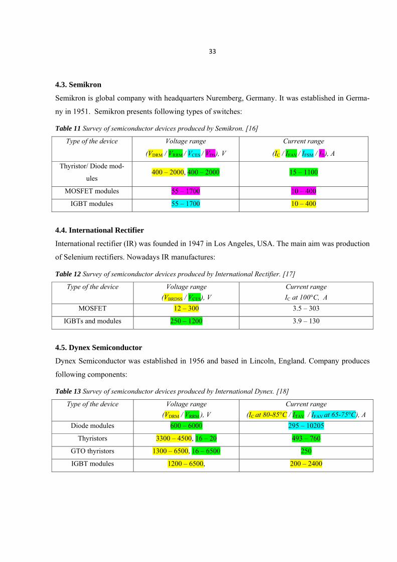
4.3. Semikron
Semikron is global company with headquarters Nuremberg, Germany. It was established in Germa-
ny in 1951. Semikron presents following types of switches:
Table 11 Survey of semiconductor devices produced by Semikron. [16]
Type of the device Voltage range
(VDRM / VRRM / VCES / VDS), V
Current range
(IC / IFAV / IFSM / ID), A
Thyristor/ Diode mod-
ules 400 – 2000, 400 – 2000 15 – 1100
MOSFET modules 55 – 1700 10 – 400
IGBT modules 55 – 1700 10 – 400
4.4. International Rectifier
International rectifier (IR) was founded in 1947 in Los Angeles, USA. The main aim was production
of Selenium rectifiers. Nowadays IR manufactures:
Table 12 Survey of semiconductor devices produced by International Rectifier. [17]
Type of the device Voltage range
(VBRDSS / VCES), V
Current range
IC at 100°C, A
MOSFET 12 – 300 3.5 – 303
IGBTs and modules 250 – 1200 3.9 – 130
4.5. Dynex Semiconductor
Dynex Semiconductor was established in 1956 and based in Lincoln, England. Company produces
following components:
Table 13 Survey of semiconductor devices produced by International Dynex. [18]
Type of the device Voltage range
(VDRM / VRRM ), V
Current range
(IC at 80-85°C / ITAV / IFAV at 65-75°C), A
Diode modules 600 – 6000 295 – 10205
Thyristors 3300 – 4500, 16 – 20 493 – 760
GTO thyristors 1300 – 6500, 16 – 6500 250
IGBT modules 1200 – 6500, 200 – 2400

34
4.6. Mitsubishi Electric
Mitsubishi Electric was founded in 1921. The company appeared after Mitsubishi Shipbuilding Co.
(now Mitsubishi Heavy Industries, Ltd.) extended activity of a factory in Kobe, Japan which made
electrical motors for ocean vessels. New company was called Mitsubishi Electric Corporation. The
head office is situated in Tokyo, Japan.
Table 14 Survey of semiconductor devices produced by Mitsubishi Electric. [19]
Type of the device Voltage range
(VDRM / VRRM / VCES / VDSS), V
Current range
(IC / ID / ITAV / ITQRM / IF), A
Diode modules 300 – 6500 (max) 6.6 – 1200 (max)
Thyristor modules 300 – 1600 (min),
300 – 1600 (min) 10 – 200 (min)
GTO Thyristors 2500 – 6000 1000 – 6000 (min)
GCT Thyristors 6500 (max), 6500 (max) 400 – 1500 (max)
Power MOSFET mod-
ules 75 – 150 100 – 300
IGBT modules 600 – 1700 50 – 1000
4.7. Hitachi
Hitachi was founded in 1910 in a small Japanese town of the same name. Now headquarters of Hita-
chi is in Tokyo, Japan. Production of Hitachi is presented in the table below.
Table 15 Survey of semiconductor devices produced by Hitachi. [20]
Type of the device Voltage range
(VRRM / VCES ), V
Current range
(IC / IFAV), A
Power Diodes 100 – 14000 0.035 – 3
IGBTs 1200 – 6500 100 – 3600
4.8. Toshiba
Toshiba was established in 1875 Japan. Today it is a global network with headquarters in Tokyo,
Japan. Company presents following devices:

35
Table 16 Survey of semiconductor devices produced by Toshiba. [21]
Type of the device
Voltage range
(VDSS / VDS / VCES at 25°C / VRRM),
V
Current range
(ID / IC /I0), A
Diodes 100 – 1000 0.2 – 100
MOSFETs -60 – 150, 600 – 650 -120 – 50
IGBTs 400 – 1500 5 – 60
4.9. Fuji Electric Systems
Company was founded in 1923 in Japan. Headquarter of company is in Tokyo, Japan. Fuji
produces following range of semiconductor switches:
Table 17 Survey of semiconductor devices produced by Fuji Electric Systems. [22]
Type of the device Voltage range
(VRRM / VCES / VDSS), V
Current range
(I0 / ID / IC), A
Diodes 20 – 800 0.5 – 30
Power MOSFETS -60 – 900 -25 – 100
IGBTs and modules 600 – 1700 2.5 – 3600
4.10 IXYS
IXYS started its activity in 1983 in a Silicon Valley, USA. Nowadays it manufactures:
Table 18 Survey of semiconductor devices produced by IXYS. [23]
Type of the device Voltage range
(VCES / VDSS / VRRM / VDRM), V
Current range
(IC / ID / IFAV / ITAV at 55°C), A
Diodes 200 – 6000 130 – 3770
Thyristors 600 – 4500, 200 – 4000 16 – 6974
Power MOSFETs and modules -600 – 4000 -140 – 340
Power IGBT and modules 600 – 4500 160 – 2400
4.11. Powerex
Powerex was established in 1986. Company was a result of consolidation of the Power Semiconduc-
tor Divisions of General Electric Company (GE) and Westinghouse Electric Corporation. At present

36
GE and Mitsubishi Electric share equal ownership of Powerex. Headquarters of company is in
Youngwood, Pennsylvania. List of production is in the Table 19.
Table 19 Survey of semiconductor devices produced by Toshiba. [24]
Type of the device Voltage range
(VCES / VDSS / VRRM / VDRM), V
Current range
(IC / ID / ITAV at 80°C), A
Diode and Thyristor
modules 600 – 6500 20 – 2000
Discrete rectifiers 200 – 6500, 200 – 6500 51 – 2500
Discrete Thyristors 200 – 6500, 200 – 6500 40 – 5000
MOSFET modules 75 – 1200 100 – 600
IGBTs 250 – 6500 10 – 1500
4.12. Fairchild Semiconductor
Fairchild semiconductor was founded in 1957 in Santa Clara Valley (also known as Silicon Valley),
in Northern California, USA. Nowadays company has headquarters in San Jose, USA.
Table 20 Survey of semiconductor devices produced by Fairchild Semiconductor. [32]
Type of the device Voltage range
(VCES / VDS / VRRM / VDRM), V
Current range
(IC / ID / IFAV), A
Diodes and rectifiers 50 – 1000 0.5 – 35
MOSFETs 12 – 1000 -50 – 277
IGBTs 300 – 1500 2.7 – 180
4.13. JSC «Electrovipryamitel»
This factory was established in 1941 in Saransk, Russia. The headquarters of company is in the
same city. Nowadays it is probably the most powerful Russian factory of semiconductor devices.
Table 21 Survey of semiconductor devices produced by JSC «Electrovipryamitel». [25]
Type of the device Voltage range
(VCES / VRRM / VDRM), V
Current range
(IC/ IRRM / IDRM), A
Diodes and modules 100 – 6000 3 – 150
Thyristors and modules 100 – 6000, 3 – 1000
IGBT modules 600 – 6500 600

37
4.14. JSC «Proton–Electrotex»
Proton-Electrotex was founded in 1996 in Orel city, Russia. It is young and promising company,
which presents next devices:
Table 22 Survey of semiconductor devices produced by JSC «Proton–Electrotex». [26]
Type of the device Voltage range
(VCES / VRRM / VDRM), V
Current range
IAV, A
Diodes and Diode mod-
ules 400 – 4400 68 – 7100
Thyristors and Thyristor
modules 100 – 6500 160 – 3600
4.15. Resultant comparison of manufacturers
Comparison of range of produced switches, which is based on tables in section 4, can be made. Ta-
bles 9-22 give an understanding of availability of different components and their voltage and current
ranges. Table 23 gives possibility to estimate the amount of companies producing every kind of
switches.
The most interesting voltage range for this study is 6.5 kV and upper, but for the commercial market
6.5 kV is a limit for fully controlled switches nowadays. At present in the medium voltage drives
only IGBT and IGCT can be applicable and will provide this voltage. Information about manufac-
turers who produce these devices with the highest current data also is shown in the Table 23.

38
Table 23 Comparison of production lines of the main players on the semiconductor market.
Manufacturer\devices Diode Thyristor GTO IGCT MOSFET IGBT
ABB + + +
Asymmetric:
VDRM=6500V,
ITGQM=3800A.
Reverse cond.:
VDRM=5500V,
ITGQM=1800A.
VCES=6.5kV,
IC=750A.
Infineon Technologies
(Eupec) + + +
VCES=6.5kV,
IC=750A.
Semikron + + + +
International Rectifier + +
Dynex Semiconductor + + + VCES=6.5kV,
IC=400A.
Mitsubishi Electric + + + VDRM=6500V,
ITQRM=1500A. + +
Hitachi + VCES=6.5kV,
IC=750A.
Toshiba + + +
Fuji Electric Systems + + +
IXYS + + + VCES=6.5kV,
IC=600A.
Powerex + + + +
JSC «Electrovipryamitel» + + VCES=6500V,
IC=600A.
JSC «Proton–Electrotex» + +
Fairchild Semiconductor + + +
If to analyze the thyristor group (thyristor, GTO, IGCT), it is obviously that thyristor is the most
available device, but GTO and IGCT are not very available, because only three companies produce
first device and only two produce the second one.
While analyzing availability of IGBT, it becomes evident that it hasn’t any competitors and con-
sumers have great possibility of choice between different manufacturers. This follows that nowadays

39
all main players of the semiconductor market produce IGBT. It shows that IGBT is the most availa-
ble device for the MV drives. IGCT is maybe the best component for the upper rates of voltage in
medium voltage and for high-voltage drives, at least till time at which there isn’t IGBT of the same
voltage ratings.

40
5. IGBT STRUCTURE TECHNOLOGIES
First generation of IGBT was produced in the end of 1980’s of the last century. The first generation
switches were quite slow in switching and inclined to failure. Second and third generations appeared
in the early 1990’s and were much improved. Development of devices goes in the direction of the
increase working voltages and currents, efficiency and reduction of static and dynamic losses. Also
in process of improvement of characteristics of IGBT, the thickness of crystal is decreased. Nowa-
days PT IGBT, Non-PT IGBT and DS Trench IGBT generations are manufactured.
Today there are 600V, 1200V, 1700V, 2500V, 3300V, 6500 IGBTs on the market and developers
permanently try to increase these ratings.
Figure 12 a) Punch-through IGBT structure, b) Non-punch-through IGBT structure, c) Trench IGBT struc-
ture. [17]
5.1. Punch-through (PT-IGBT)
Punch-through IGBT is used quite thick chips made from epitaxial wafers with additional
buffer N+ layer, which plays role of field stop layer. Extra layer has two general functions: avoids
failure by punch-through action because the depletion region expansion at applied high voltage is
restricted by this layer and reduces the tail current during turn-off and shortens the fall time of the
IGBT, because the holes are injected by the P+ collector partially recombine in this layer. The small

41
tail current is a typical characteristic of NPT-IGBTs. The thickness of crystal of PT-IGBTs is more
than 300 µm. PT-IGBT structure is presented on the Figure 12a.
5.2. Non-punch-through (NPT-IGBT)
Non-punch-through IGBT has P-N-P-N structure, which is very similar to structure of power
MOSFET except of P+ injecting layer. For the N-type IGBT, which is presented in the Figure 10a,
N+ layer on the top is emitter and P- on the bottom is collector. Transistor can be P-type. In this case
the structure of the device is reversed. NPT-types have thinner chips, which are lower cost, because
they haven’t extra N+ layer. The thickness of IGBT crystal is about 87 µm. NPT-IGBT structure is
depicted on the Figure 11b.
NPTs are medium speed switches, so they have a good balance between switching and conduction
losses.
NPT-IGBTs have the same forward and reverse breakdown voltages, therefore they are proper for
AC applications. PT-IGBTs have less reverse breakdown voltage than forward breakdown voltage,
so they are more suitable in DC circuits, where there isn’t necessity to conduct in reverse direction.
The comparison table of PT- and NPT- types of transistors was made by Abdus Sattar from IXYS
Corporation. This research is presented in the Table 24.
Table 24 Comparison of PT- and NPT-IGBT. [31]
Characteristic\ Type of IGBT PT NPT
Switching loss Low
Short tail current. Significant
increase in EOFF with T
Medium
Long, low amplitude tail current.
Moderate increase in EOFF with T
Conduction loss Low
Flat to slight decrease with T
Medium
Increases with T
Paralleling Difficult
Must sort on VCE(ON)
Easy
Optional sorting. Recommend
share heat
Short-circuit rated Limited
High gain
Yes

42
PT-IGBT and NPT-IGBT have planar cell design for the gate-emitter structure.
5.3. Soft-punch-through/ Light-punch-through IGBT (SPT/LPT-IGBT)
Soft-punch-through concept is based on the usage of low doped N-buffer layer on the anode side of
the IGBT. SPT-type took best qualities from each of PT and NPT. In comparison to existing NPT
technology, SPT has 20% lower on-state losses, 20% lower switching losses and it hasn’t increase of
thermal resistance. Relative comparison of new modification with traditional NPT was made by
ABB and presented on the Figure 11.
Figure 13 Comparison of SPT and NPT. [33]
Soft-punch-through IGBT was designed for using in the LoPak modules. Owing to its resistive char-
acteristics, SPT is well suited to parallel connection. [33], [34]
5.4. Depletion stop/ Field stop trench IGBT
The next generation of IGBT has trench design of gate-emitter structure. It contains vertical gate and
depletion layer, which is also known as a field stop layer. The thickness of crystal becomes about 70
µm. Structure is shown on the Figure 12c.
Trench cell design has very low VCE(ON), because it increases channel density and reduces the re-
sistance of JFET, which was typical for the planar structure. Trench IGBTs have lower conduction
losses and switching losses. It is particularly valuable in the low frequency applications, where low
conduction losses are most important.

43
Figure 14 Benefits of trench structure over planar structure. [35], [36]
With help of Figure 12 it is evident how the structure of IGBT and thickness of crystal was changed
during the development of IGBT.
5.5. Injection enhanced gate transistor (IEGT)
This device unites advantages of traditional IGBTs: low power for operation and large safe opera-
tional area. MOS gate structure in IEGT works as an emitter with high electron injection and it
stores high amount of carriers in the N-type high resistance base layer at the emitter side. IEGT has
similar on-state characteristics with a thyristor. This switch has high current capability which de-
mands high short circuit ability. Like a thyristor it has same distribution of current density and low
forward voltage drop. These differs IEGT from conventional IGBT. IEGT also can have planar
structure. Example of trench structure IEGT is depicted on the Figure 15a. [51]
5.6. Carrier stored trench bipolar transistor (CSTBT)
CSTBT is quite new invention of Mitsubishi Electric. Device has advantages of the conventional
trench structure IGBT. In addition to traditional structure CSTBT has extra N-type layer in the emit-
ter side for the carrier storing. The concentration of the N layer, which is known as conservation of
charge layer, is higher than the N-layer, thus N layer can control the shift of holes to the P base. The
function of charge conservation significantly improves characteristics of the on-state in comparison
with traditional trench IGBT. CSTBT structure is depicted on the Figure 15b and can be compared
with IEGT structure (Figure 15a) and classical trench IGBT structure (Figure 12c). [50]

44
Figure 15 a) Current density and IEGT structure, b) CSTBT structure. [50], [51]

45
6. CHARACTERISTICS OF IGBT
Examples of characteristics were taken from the datasheet of FZ750R65KE3T IGBT with VCES=6.5
kV/ IC_NOM=750 A, produced by Infineon Technologies.
6.1. Static characteristics
In the on-state VCE depends on IC, VGE and TJ. VCE presents voltage drop while IGBT is conducting.
It shows dissipation losses, therefore collector-emitter voltage should be as low as possible. VCE in-
creases in direct proportion to IC and inversely proportional to VGE. If value of IC is small, while TJ
increases, so VCE decreases and vice versa, if IC is large and TJ increases, so VCE increases. [37]
Figure 16 IC – VCE(SAT) – VGE characteristics of FZ750R65KE3T. [45]
6.2. Switching characteristics
First of all switching losses appear because of slow elimination of holes in the drift layer after the
VGE became lower than the threshold voltage, which turns off the switch. The holes recombine or are
swept out by the voltage deviation. This process causes current tail. For example in PT-IGBTs addi-
tional buffer layer quickly absorbs remaining holes.
At higher IC or TJ, the switching time increases causing higher losses. When IGBT is used in differ-
ent assemblies like inverter, switching time can exceed dead time of the adjacent IGBT which lead
to short circuit. If t9-t10 or tF (Figure 18b) is too short, the transient current will rapidly change (di
dt)

46
and because of the circuit inductance, voltage spike will occur (di
Ldt
). The gate resistance also in-
fluences on losses with direct proportion.
Switching losses EON and EOFF occurs permanently during the switching, so they should be mini-
mized as much as possible. [36], [37]
Figure 17 Switching losses of IGBT: a) EON, EOFF – RG curves, b) EON, EOFF – IC characteristics of
FZ750R65KE3T. [45]
6.3. Gate resistance
Process of gate charge is controlled by gate resistance. If the resistance is smaller, so loss and
switching times will be smaller, but in this case noises can appear. If IGBT is used with FWD in
module, smaller values of RG follows to switching on higher di
dt, therefore diode has to recover on
higher du
dt which cause overvoltage transients. RG influences on RBSOA and SCSOA (more in de-
tails about SOAs in chapter 6.5). The rated value is usually given in datasheets by manufacturers
and example of dependence of dissipated energy form gate impedance is illustrated on the Figure
17a. [38]
Turn-on characteristics are determined by MOSFET part of structure and they are influenced by the
gate drive impedance. Turn-off characteristics are determined by the minority carriers recombina-

47
tion, which is indirectly influenced by MOSFET turn-off. Increasing of gate drive resistance contin-
ues the Miller effect and causes delay in the current fall, which also is named as current tail. Current
tail can be seen on the Figure 18b on the time interval t10-t11. Turn-on losses appear in switches in-
dependently on the speed of switching, whereas turn-off losses depend on the speed of IGBT. This
way fast IGBT will be less affected by the qualities of gate drive impedance, than ultrafast IGBT.
Thus ultrafast IGBT should have lower gate drive impedance than fast IGBT.
Figure 18 Typical switching characteristics of IGBT. a) Turn-on, b) Turn-off. [38]
It should be mentioned that in different sources gate resistance is named as gate impedance. From
the point of view of classical physics it is wrong substitution, but in case of
48
semiconductor devices both of these definitions suppose resistance or active power dissipation.
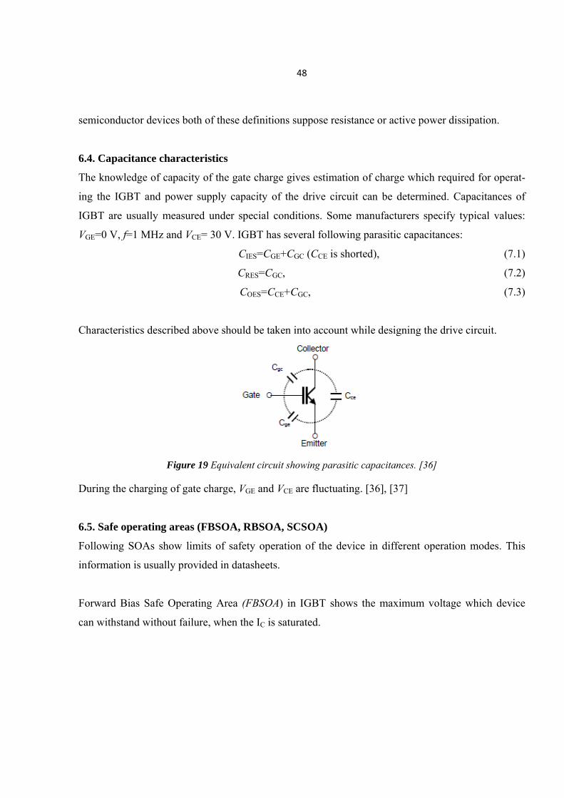
6.4. Capacitance characteristics
The knowledge of capacity of the gate charge gives estimation of charge which required for operat-
ing the IGBT and power supply capacity of the drive circuit can be determined. Capacitances of
IGBT are usually measured under special conditions. Some manufacturers specify typical values:
VGE=0 V, f=1 MHz and VCE= 30 V. IGBT has several following parasitic capacitances:
CIES=CGE+CGC (CCE is shorted), (7.1)
CRES=CGC, (7.2)
COES=CCE+CGC, (7.3)
Characteristics described above should be taken into account while designing the drive circuit.
Figure 19 Equivalent circuit showing parasitic capacitances. [36]
During the charging of gate charge, VGE and VCE are fluctuating. [36], [37]
6.5. Safe operating areas (FBSOA, RBSOA, SCSOA)
Following SOAs show limits of safety operation of the device in different operation modes. This
information is usually provided in datasheets.
Forward Bias Safe Operating Area (FBSOA) in IGBT shows the maximum voltage which device
can withstand without failure, when the IC is saturated.

49
Figure 20 a) RBSOA of IGBT, b) SOA of FWD of FZ750R65KE3T. [45]
Reverse Bias Safe Operating Area (RBSOA) is area of safe operation of the IGBT, during the switch
off. RBSOA gives maximum values of voltage and currents which the component is capable to
switch. The maximum IC is usually 200% of rated current at 85 % of VCES, with TJ=125°C. As op-
posed to FBSOA in RBSOA a snubber circuit is important for safe switching off.
Short Circuit Safe Operating Area (SCSOA) determines borders of safe operation during the fault.
Example of SOAs is depicted on the Figure 20 on the previous page. [36], [37], [38]
6.6. Internal diode (FWD) characteristics
Free wheel diode connected in anti-parallel with IGBT. It allows module to conduct in reverse direc-
tion. This made when inductive load is used. FWD prevents voltage spike in case of change or re-
duction of voltage over the inductive element.
Characteristics of diode depend on IC and TJ. Diode current ratings IF are usually about 2
3 of nomi-
nal IGBTs ratings. Blocking voltage and junction temperature are the same to IGBT. Figure 21 pre-
sents example of main characteristics of FWD. [37], [38]

50
Figure 21 IF – VF characteristics of the FWD of FZ750R65KE3T. [45]
6.7. Transient thermal resistance characteristics
During the work IGBT module dissipates energy in form of heat. This makes worse characteristics
and reduces the lifetime of the equipment. Transient thermal characteristics are used to calculate the
temperature rise of the module and the heat sink should be chosen relying on these results. Example
of dependence of thermal impedance from time for selected IGBT is illustrated on the Figure 22.
Figure 22 Thermal impedance – time characteristics of a) IGBT b) FWD of FZ750R65KE3T. [37]

51
Thermal characteristics include ZTH and RTH. ZTH shows the change of temperature of the device in
time. RTH shows the conduction properties of the switch and it can be divided on several parts (equa-
tion 7.4). [36], [38]
ZTH=ZTH(JC)+ZTH(HA)+ZTH(CH), (7.4)

52
7. CONNECTION OF IGBT
7.1. Series connection of IGBT
Permanent grow of voltage ratings leads to necessity connect either one powerful switch or several
in series connection. Series connection hasn’t lost its urgency even with development of 6.5 kV
power devices. Series connection strongly depends on device characteristics and mismatching of the
drive circuit. Turn-off of series connected devices has difficulty appearing because of following fac-
tors:
Unequal device switching characteristics;
Unequal device leakage current;
Unequal stray inductance in the series circuit;
Unequal gate drive delay;
One of important moments in series operation is to match static and dynamic balancing of voltages.
The problem of static voltage balancing can be easily solved by adding a resistor in parallel connec-
tion with each switch. There are two available dynamic voltage balancing technics: load side balanc-
ing and gate side balancing. The load side balancing demands a snubber circuit and a clamp circuit.
This scheme is not applicable in high voltage application, because these circuits cause high losses
which directly proportional to switching frequency. On the contrary active gate control may be more
preferable. [60]
7.2. Parallel connection of IGBT
Modern high power applications and industrial drives require switches which can handle high volt-
ages and currents. The solution is parallel connection of components. A difference of output charac-
teristics of parallel connected IGBT can cause a voltage and current imbalance. This is shown on the
Figure 23b.

53
Figure 23 a) Parallel connection of IGBT, b) IC – VCE(SAT). [37]
The output characteristics of IGBT are expressed in equations 8.1 – 8.4.
CE_Q1 01 1 1CV V r I , (8.1)
1 1 C1 C2/ ( )r V I I , (8.2)
CE_Q2 02 2 C2V V r I , (8.3)
2 2 C1 C2/ ( )r V I I , (8.4)
It is evident that total current in parallel connection of switches is a sum of currents through the de-
vices:
C_TOTAL C1 C2I I I , (8.5)
Consequently, collector currents of each IGBT can be derived as following:
C1 02 01 2 C_TOTAL 1 2( ) / ( )I V V r I r r , (8.6)
C2 01 02 1 C_TOTAL 1 2( ) / ( )I V V r I r r , (8.7)
VCE(SAT) is the principal factor which influences on the appearance of imbalance, so it is very im-
portant to select devices with similar value of VCE(SAT). [37]
It is impossible to exactly avoid imbalance only by choosing right semiconductor switches, so there
are several voltage/current balancing technics which are shown on the Figure 24. This thesis doesn’t
tell in details about these technics, their advantages and disadvantages, but only shows existing vari-
ety of them and points out the appearance of problems while using parallel connection.
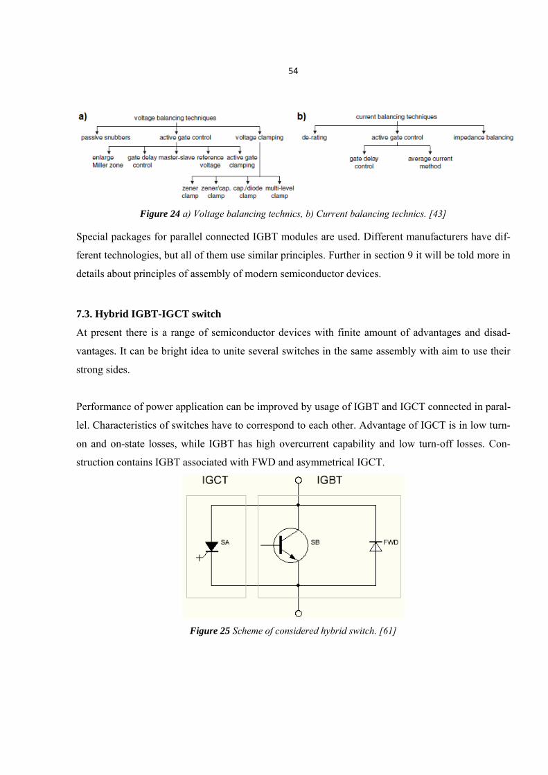
54
Figure 24 a) Voltage balancing technics, b) Current balancing technics. [43]
Special packages for parallel connected IGBT modules are used. Different manufacturers have dif-
ferent technologies, but all of them use similar principles. Further in section 9 it will be told more in
details about principles of assembly of modern semiconductor devices.
7.3. Hybrid IGBT-IGCT switch
At present there is a range of semiconductor devices with finite amount of advantages and disad-
vantages. It can be bright idea to unite several switches in the same assembly with aim to use their
strong sides.
Performance of power application can be improved by usage of IGBT and IGCT connected in paral-
lel. Characteristics of switches have to correspond to each other. Advantage of IGCT is in low turn-
on and on-state losses, while IGBT has high overcurrent capability and low turn-off losses. Con-
struction contains IGBT associated with FWD and asymmetrical IGCT.
Figure 25 Scheme of considered hybrid switch. [61]

55
This idea was implemented in PSPICE software by scientists of Tallinn University of Technology.
They selected 4.5 kV press-pack switches: 5SHY35L4512 (ABB) and T0900EA45A (Westcode,
IXYS). [61] Devices have similar turn-on behavior, while at turn-off IGCT is much slower, which
causes higher losses. Switches conduct full input current, as opposed to parallel connection of same
switches. In the other point of view total power dissipation is decreased in comparison with single
switches, which allow increasing of switching frequency and reduction of cooling requirements. In
case of failure of one of switches, second is able to operate individually.
Following parameters were chosen for the simulation: the input voltage was equal 2800 V, the max-
imum load current – 750 A and the switching frequency was 750 Hz. Some results of combined
work of two devices are presented on the Figure 26.
Figure 26 a) Switching frequency – current, b) Switch power dissipation – switching frequency,
c) Breakdown of power losses. [61]

56
In spite of advantages of hybrid switch it also has disadvantages in comparison with parallel connec-
tion of same switches:
Price;
Decreased maximum current capability;
Presented hybrid switch can be useful in applications where higher frequencies and reduced
cooling systems are required. [61]

57
8. LOSS CALCULATION
As was told in the section 2.6, nowadays the most attractive semiconductor components for medi-
um-voltage drives are IGBT and IGCT, so it is necessary to compare losses of these two devices.
Methodology used for calculation of IGBT losses was taken from the application note of Infineon
Technologies. IGCT is calculated with usage of methodology of ABB. Switching frequency for both
calculations is average.
8.1. IGBT loss calculation
IGBT module FZ750R65KE3T produced by Infineon Technologies was selected for the losses anal-
ysis. This device is suit for MV converters and traction drives. VCES=6500 V, IC_NOM=750 A. As-
sume that Tj=125 °C, VGE=15 V, fSW=500 Hz.
Curves presented on the Figure 27 are taken from the datasheet of chosen device and give a possibil-
ity to get rC, rD, UCE0 and UD0.
Figure 27 Determination of a) rC of IGBT, b) rD of the diode. [47]
Received from Figure 27 values of voltages U and currents I are put into equations 9.1, 9.2:
3CEC
C
32 10
1500
Ur
I
Ohm, (9.1)
3FD
F
2.41.6 10
1500
Ur
I
Ohm, (9.2)

58
Conducting losses of IGBT and diode are calculated as follows in 9.3 and 9.4 respectively:
SW
2 3 2CT CE0 C C C
SW 0
1( ( ) ( ) ( )) 2.2 200 2 10 750 1570
T
P u i t r t i t dtT
W, (9.3)
SW
2 3 2CD D0 D D D
SW 0
1( ( ) ( )) 1.8 250 1.6 10 750 1350
T
P u i t r i t dtT
W, (9.4)
Switching losses are found by using of turn-on state and turn-off state losses in the 9.5 equation.
These values are taken from the datasheet.
3 3SWT ON OFF( ) (4200 10 3600 10 ) 500 3900P E E f W, (9.5)
Turn-on energy of the diode mostly consists of reverse-recovery energy, which is taken from
datasheet: EREC=1400 mJ, and power can be calculated as follows in 9.6:
3SWD REC 1400 10 500 700P E f W, (9.6)
Power losses of the IGBT and the diode can be determined as a sum of conductive losses and
switching losses:
TOT CT SWT CD SWD 7500P P P P P W, (9.7)
Result analysis will be made in the section 8.3. [45], [47]
8.2. IGCT loss calculation
Reverse conducting GCU08BA-130 GCT produced by Mitsubishi Electric, was selected for losses
analysis. The main reason of the choice of this model of GCT is its ability for reverse conducting
and correspondence of voltage and current to IGBT selected in the previous section. Almost all val-
ues for calculation are taken from the datasheet. Main values are VRRM/VDRM=6500V, ITQRM=800A.
For calculation of power in the on-state it is necessary to find PAV(M), ITAVM and IT(RMS). These was
made in equations 9.8-9.10.
υjmaxAVM
th(jc)
125 801800
0.025 /CT T C C
PR k W
W, (9.8)
Values of ITAVM and IT(RMS) can be taken from the datasheet.
2 2(T0) T AVM (T0)
TAVM 2T
2 330V r P V
Ir
A,
(9.9)

59
T(RMS) TAVM 330 5202 2
I I
A, (9.10)
On-state power is calculated in the 9.11. This methodology of losses calculation was taken in the
ABB tutorial, but Mitsubishi Electric does not give rT and VT0 which are necessary for calculation,
so assume that 3T 0.56 10r Ω (value was taken in the datasheet of 5SHY 42L6500 assymetric
IGCT, produced by ABB with VDRM=6500 V/ ITGQM=3800A) and assume that (T0) GT 1.5V V V
(value of VGT is the nearest to V(T0) which can be used. Officially this substitution probably is not
correct.)
2 3 2ON_STATE T0 TAV T T(RMS) 1.5 330 0.56 10 520 650P V I r I V A A W, (9.11)
Further power during the switching is found:
TURN_ON_IGCT ON 0.6 500 300P E f J Hz W, (9.12)
TURN_OFF_IGCT OFF 2.3 500 1150P E f J Hz W, (9.13)
TURN_OFF_DIODE RR 4.4 500 2200P E f J Hz W, (9.14)
The total sum of losses is presented in the equation 9.15:
ON_STATE TURN_ON TURN_OFF TURN_OFF_DIODE 4300TOTP P P P P W, (9.15)
Result analysis will be made in the section below. [48], [49], [66]
8.3. Loss calculation analysis
Received values and calculations are not verified and couldn’t be used for accurate choice of equip-
ment. Obtained results shows order of losses.
Both of switches have advantages and disadvantages. Losses calculation of single switch helps to
confirm strong and weak sides of devices in different states. Switching frequency used in calculation
was quite low and it is obvious that switching losses directly depend on frequency.
In the on-state IGCT obviously has more favourable characteristics than IGBT. It is caused by the
high impedance of IGBT in the on-state. During turn-on IGBT dissipates more energy than IGCT,
whereas during turn-off IGBT has lower losses as opposed to IGCT.

60
Table 25 Comparison of results of calculation of losses of IGBT and IGCT in different states at f=500 Hz.
State/ Device IGBT IGCT
On-state (conduction losses), W 1570+1350 (IGBT+diode) 650
Turn-on (switching losses), W 2100 300
Turn-off (switching losses), W 1800+700 (IGBT+diode) 1150+2200 (IGCT+diode)
Total losses, W 7500 4300
Total losses of IGBT are bigger than IGCT losses. It should be noticed that IGBT module contain
three single switches and each with antiparallel diode, while IGCT contains only one switch. In case
of the simplest inverter, which consists of 6 switches, it will be necessary to use only two IGBT
modules and six IGCT ones, therefore total losses of IGBT based inverter would be less.
At present IGBT and IGCT have very similar losses in the same power ratings, so sometimes it can
be very difficult to choose more appropriate switching component for some applications. In case of
low voltages of MV segment, IGBT probably will remain the most attractive semiconductor switch,
because as was told in chapter 4.15 it is the most available component.
From the point of view of ideal switch, IGCT can be named ideal in conduction state owing to its
low losses and high overload ability, whereas IGBT is ideal in turn-off state. It is evident that this
opinion is very optimistic, but it shows main idea.

61
9. FUTURE OF POWER SEMICONDUCTORS
9.1. Assemblies of IGBT
At present new demands to ease of usage and reduction of influence on the environment employ
new technologies of performance power semiconductor modules. It leads to reduction of size and
power losses and increasing of reliability in the motor controllers. Today manufacturers make an
emphasis on production devices with environmentally friendly behaviour. Contemporary switches
should be compliant with ROHS directive, which came into force in European Union in 2003. Ac-
cording to this directive all produced components have to tend to reduction of amount of used haz-
ardous substances.
There is a tendency to assemble several arrangements in the same case. It allows reducing size and
weight of the equipment. In addition to modules companies develop hybrid devices which unite ad-
vantages of several other devices. At present hybrid integrations can be divided on following
groups: module, IPM, intellectual subsystem and intellectual electronic power system. This is de-
picted on the Figure 28.
Figure 28 Levels of hybrid system integrations. [52]

62
Table 26 presents different power modules which tend to minimization and size effectiveness.
Table 26 Levels of system integration. [52]
Number of level of system
integration
Examples of power modules Assembly
1 Econopack (Infineon), LoPak 3, 4, 5
(ABB), SKiM 4, 5 (Semikron)
IGBT modules, diode rectifiers
with system for breaking
2 IPM produced by Mitsubishi, Fuji,
Hitachi
3 phase bridge inverter, schemes
of operation and blocks of protec-
tion
3 SKiiP (Semikron) Power modules with built-in driv-
er, voltage sensors and overvolt-
age protection on the DC bus
which are mounted on the liquid
cooling system.
Reduction of size and desire to gather as much components as possible in one case lead to improve-
ment of reliability, reduction of losses and finally reduction of price. The main reason of reduction
of losses is absence of large number of long connecting wires and additional components.
9.2. Perspectives of development of the semiconductor industry
Power ratings of semiconductor devices will constantly increase. Mostly it will be realized by thin-
ning and changing the crystal structure. Second main change concerns to the material of crystal in
devices.
In November 2009 semiconductor division of ABB presented 10 kV IGCT. This element will be
focused on speed-controlled drives for MV motors, rail network interconnections in frequency and
energy management systems, also this device can be used in HVDC and FACTS applications. Gen-
eral investigation was emphasized on increasing the robustness against cosmic ray radiation. While
blocking voltage of IGCT was increased from 6.5 kV to 10 kV, its switching properties became sig-
nificantly worse and therefore SOA was reduced. It demanded to develop new structure. One of the
difficult tasks was to create freewheeling diode corresponding new IGCT. Standard high-voltage
diodes often oscillate at high voltages. It leads to huge over-voltages and high-frequency current os-
63
cillations during the turn-off and reverse recovery. This required making changes in the diode struc-
ture, so diodes acquired soft switching characteristics. Creation of 10 kV device makes possibility
for operation of 12 MW drives with 7.2 kV input voltage. Nowadays 10 kV IGCT is not presented
on the semiconductor market. Its presentation is planned on the 2011. [14]
Future of semiconductors will be uninterruptedly related with development of new materials. Mate-
rials with wider band gap than Si, like SiC and GaN, will be used in a few years. 10 kV SiC
MOSFET with ID=10 A was created quite recently. In comparison with standard 6.5 kV IGBT it
presents approximately only 1
200th of total switching energy of the IGBT. In spite of quite low
power this device can be successfully used in PV panels. SiC MOSFET is a good reason for expect-
ing the development of high power SiC IGBT with voltage more than 10 kV. 12 kV IGBT based on
4H-SiC has already been created. [55], [56], [57]
Manufacturers permanently try to increase reliability of semiconductor components, but sometimes
reliability depends on external factors. Influence of cosmic rays on high current and voltage devices
was revealed in early 1990’s. This kind of radiation can disturb normal operating state of series of
devices. All kind of semiconductor components can be exposed to suffer under the cosmic rays and
risk of failure is higher as the altitude above the sea level is higher. Today contemporary high power
components are designed in conditions while failure rate due to the action of cosmic rays is reduced
to an admissible level. In future probably this failure rate will be reduced while semiconductor tech-
nology will be more developed.

64
CONCLUSIONS
From the second half of the last century, when first semiconductor devices were created, industry is
constantly developed. At present power electronics is used almost in all technological processes and
home appliances. Mostly power switches are utilized in DC/AC converters. Dimensions, efficiency
and reliability of converter depend on the amount of switches, therefore creation of devices of high-
er voltage and current ratings allows to reduce usage of series or parallel connection. Main problem
of series and parallel connection is a discrepancy of characteristics of components, which causes
voltage and current imbalance. DC/AC converters are fundamental elements of power drives. Elec-
trical drives are widely used almost in all fields of industry and it is very important to improve oper-
ation characteristics of drives in order to improve efficiency of the whole manufacture.
Today there are several semiconductor switches, which have advantages, disadvantages and can be
chosen properly in respect to their characteristics. Classical SCRs are successfully applicable in
high-voltage and high-power applications, like HVDC and different FACTS equipment. Thyristors
nowadays are the most powerful devices. GTO owing to its ability for controlled operation can be
used in adjustable drives and also in energy networks, like thyristors. MOSFET is the fastest switch,
but it is not suitable for MV range. Even if to take into account the creation of 10 kV SiC MOSFET
with ID=10 A, its power is about 100 kW, which is much less than average power ratings of MV
range. For usage in power drives IGBT and IGCT are the most applicable switches. They have quite
equal losses, but IGCT is better in the on-state and IGBT is better during the turn-off. This was
proved by the calculation of losses. Calculation in this thesis doesn’t show exact losses of switches
and can’t be used for selection of devices, but it shows an order of losses and gives understanding of
strong and weak sides of components.
One the most decisive factors which can mark out the switch towards other is the price. Unfortunate-
ly this information is much hidden, because of the hard competition between manufacturers. Thus
thesis could not make a comprehensive analysis of price of different devices. But it answered the
question about availability. It becomes evident that IGBT is produced by all main producers of sem-
iconductor components, whereas IGCT is manufactured only by two of them.
65
IGBT was selected as a basic component in this study. Development of structure of IGBT was con-
sidered. It is obvious that dimensions of crystal are reduced, but voltage and current ratings are in-
creased from the development of the first IGBT. Thus manufacturers after years of development
created trench structure, which has more favourable characteristics over planar structure. Today fur-
ther development mostly depends on the usage of new materials with wide band gap, like SiC and
GaN. Creation of IGBT with voltage ratings more than 10 kV is a step in this direction. In recent
years 12 kV IGBT has already been created and it is a very promising switch.
Nowadays manufacturers tend to minimize and optimize power modules. This way they try to unite
several components into one case and receive intellectual subsystems and intellectual electronic
power systems. This reduces dimensions and weight of equipment and consequently less length of
required bonding wires. Thus losses can be reduced and efficiency can be increased. One of the
most topical questions for every field of industry is the influence of equipment on the environment.
Some producers follow ROHS directive and usually mention this fact in datasheets.
The main conclusion which can be made is that for nowadays IGBT is the most attractive semicon-
ductor switch for lower voltage rates in MV drives. It has several disadvantages which give to IGBT
unprofitable appearance. This switch has the highest losses in the on-state over other switches which
are caused by collector-emitter voltage, which should be low as possible. VCE increases in direct
proportion to IC and inversely proportional to VGE. VCE and IC depend on the temperature of junction.
Switching losses are caused by slow elimination of holes in the drift layer after VGE became lower
than the threshold voltage, which turns off the switch. This forms current tail which is inherent to
IGBT. Gate resistance of IGBT is also influences on the energy dissipation and it is directly propor-
tional to appearing losses. RG influences on RBSOA, SCSOA and modes of FWD conduction. FWD
in IGBT can be a powerful source of losses, therefore diodes for high-voltage switches in voltage
ratings more than 6.5 kV were improved. FBSOA, RBSOA and SCSOA limit safe operation of de-
vice. But in spite of described above disadvantages IGBT has better switch-off characteristics than
all switches of the thyristor group.
For higher voltage levels of MV rate IGCT is the only suitable switch. It has much lower conduction
losses than IGBT and high overload ability, but it is worse during the switching off and needs addi-

66
tional inductance in the circuit which limits current spikes and protects FWD. During the turn-on
IGBT and IGCT have quite similar characteristics.
Today developers of MV drives have good and suitable solutions for constant growth of efficiency
and reduction of losses in their equipment in all power and voltage ratings. Nowadays there are wide
possibilities of accurate selection of semiconductor components for all needs. In future these possi-
bilities will be only expanded.

67
REFERENCES
[1] Mohan, N., Undeland, T.M., Robbins, W. 2003. Power Electronics. Converters, Applications
and Design. 3rd ed. USA. John Wiley & sons, Inc.
[2] Bose, B.S. 2001. Modern Power Electronics and AC Drives. Prentice Hall.
[3] http://upload.wikimedia.org/wikipedia/commons/c/c5/Thyristor.svg,
http://upload.wikimedia.org/wikipedia/commons/6/69/Mosfet_saturation.svg,
http://upload.wikimedia.org/wikipedia/ru/d/df/IGBT_Tr_Stuct.jpg.
[4] http://sub.allaboutcircuits.com/images/03206.png,
http://sub.allaboutcircuits.com/images/03310.png,
[5] Rogachev, K. Contemporary Gate turn-off thyristors.
[6] Medium voltage thyristors K0349LC600 to K0349LC650 datasheet. 2002. USA. IXYS Compa-
ny.
[7] S. Klaka, S. Linder, M. Frecker A new range of reverse conducting gate-commutated thyristors
for high-voltage, medium power applications. Lenzburg, Switzerland. ABB Semiconductors AG.
[8] Asymmetric Gate turn-off Thyristor 5SGF 40L4502 datasheet. 2005. Switzerland. ABB Switzer-
land Ltd, Semiconductors.
[9] IGCT Flyer. IGCTs – Integrated Gate-Commutated Thyristors. 2010. Switzerland. ABB Switzer-
land Ltd, Semiconductors.
[10] IRFP4242PbF MOSFET datasheet. 2009. USA. International Rectifier.
[11] IGBT Module 5SNA 0750G650300 datasheet. 2009. Switzerland. ABB Switzerland Ltd, Semi-
conductors.
68
[12] Alex Q. Huang, Kevin Motto, Yuxin Li. Development and Comparison of High-Power Semi-
conductor Switches. 2000. USA. Bradley Dept. of Electr. & Comput. Eng., Virginia Polytech. Inst.
& State Univ., Blacksburg, VA.
[13] Prabhuraj Bhooplapur, Benoit P. Schmitt, Gerhard Neeser. HV-IGBT Drives and Their Appli-
cations. 1999. Hong Kong. IEEE 1999 International Conference on Power Electronics and Drive
Systems.
[14] Web site of ABB. Semiconductor section.
http://www.abb.com/product/us/9AAC910029.aspx?country=FI.
[15] Web site of Infineon Technologies. http://www.infineon.com.
[16] Web site of Semikron. http://www.semikron.com.
[17] Web site of International Rectifier. Product line: http://www.irf.com/search/product_line.html.
[18] Web site of Dynex Semiconductor. http://www.dynexsemi.com.
[19] Web site of Mitsubishi Electric. Semiconductor section.
http://www.mitsubishichips.com/Global/index.html.
[20] Web site of Hitachi. Power semiconductor section.
http://www.hitachi.co.jp/products/power/pse/.
[21] Web site of Toshiba. Electronic components section. http://www.toshiba-components.com/.
[22] Web site of Fuji Electric. Semiconductor section.
http://www.fujielectric.com/products/semiconductor/products/index.html.

69
[23] Web site of IXYS. Power devices section.
http://www.ixys.com/Product_portfolio/power_devices.asp.
[24] Web site of Powerex. http://www.pwrx.com;
[25] Web site of Electrovipryamitel. Production list. http://www.elvpr.ru/en/products/index.php.
[26] Web site of Proton-Electrotex. Production list. http://proton-electrotex.com/eng/product.
[27] Marioara Avram, G. Brezeanu, A. Avram, Otilia Neagoe, M. Brezeanu, C. Iliescu, Cecilia
Codreanu, C. Voitincu. 2005. National Institute for Research and Development in Microtechnolo-
gies. Bucharest, Romania.
[28] S. Bernet, R. Teichmann, A. Zuckerberger, P. Steimer. Comparison of High Power IGBTs and
Hard Driven GTOs for High Power Inverters. 1998. Germany. ABB Corporate Research. Switzer-
land. ABB Industrie AG. R&D Drives and Power Electronics.
[29] Navid Zargari, Steven Rizzo. Medium Voltage Drives in Industrial Applications. Rockwell Au-
tomation. Cambridge, ON.
[30] Juha Pyrhönen. Electrical drives 2010…2011. Lecture notes. Finland. Lappeenranta University
of Technology.
[31] Abdus Sattar. Insulated Gate Bipolar Transistor (IGBT) Basics. IXYS Corporation. IXAN0063.
[32] Web site of Fairchild Semiconductor. Production list.
http://www.fairchildsemi.com/products/index.html.
[33] M. Rahimo, W. Lukasch *, C. von Arx, A. Kopta, R. Schnell, S. Dewar, S. Linder. 2001. Novel
Soft-Punch-Through (SPT) 1700V IGBT Sets Benchmark on Technology Curve. ABB Semiconduc-
tors AG, Lenzburg, Switzerland. * Semikron Elektronik GmbH, Nuremberg, Germany.

70
[34] Steve Dewar and Egon Herr. 2001. Soft Punch Through IGBTs in LoPak Modules Boost Pow-
er. Available at http://powerelectronics.com/mag/power_soft_punch_igbts.
[35] Chiu Ng, Al Diy, Alberto Fernandez, Vijay Bolloju. Application Note AN-1086. BVCES Testing
Considerations for Ultra-thin wafer Depletion Stop Trench IGBTs.
[36] By Vijay Bolloju, Ritu Sodhi, Chiu Ng, Jie Zhang. 2006. Trench IGBTs Improve Appliance
Motor Drives. International Rectifier, El Segundo, Calif.
[36] Application Note 9016. IGBT Basics 1. February, 2001. Fairchild Semiconductor Corporation.
[37] IGBT Modules Application Manual. February 2010. FUJI ELECTRIC SYSTEMS Co., Ltd.
[38] AN4504. IGBT Ratings and Characteristics. Application Note. July 2002. DYNEX Semicon-
ductor LTD.
[39] Jon Mark Hancock. Meeting Future Application Challenges in HV Semiconductors. Infineon
Technologies NA, Inc. Available at http://www.apec-conf.org/2004/APEC04_SP3-6_Infineon.pdf.
[40] Nimrod Vázquez, Member, IEEE, Hector López, Claudia Hernández, Member, IEEE,
Eslí Vázquez, René Osorio, and Jaime Arau, Senior Member, IEEE. August 2010. A Different Mul-
tilevel Current-Source Inverter. IEEE TRANSACTIONS ON INDUSTRIAL ELECTRONICS,
VOL. 57, NO. 8.
[41] S. Thangaprakash and A. Krishnan. June 2010. Implementation and Critical Investigation on
Modulation Schemes of Three Phase Impedance Source Inverter. Iranian Journal of Electrical &
Electronic Engineering, 84 Vol. 6, No. 2.
[42] Björn Backlund, Eric Carroll. August 2006. Voltage ratings of high power semiconductors.
Product Information. ABB Switzerland Ltd Semiconductors. Available at http://search-

71
ext.abb.com/library/Download.aspx?DocumentID=5SYA2051-
00&LanguageCode=en&DocumentPartID=&Action=Launch.
[43] N.Y.A. Shammas, R. Withanage and D. Chamund. Review of series and parallel connection of
IGBTs. February 2006. IEE Proc.-Circuits Devices Syst., Vol. 153, No. 1.
[44] Franz Auerbach (Infineon Technologies), Josef Georg Bauer (Siemens AG), Manfred
Glantschnig (Infineon Technologies), Juraen Gattert (eupec GmbH & CO KG), Martin Hierholzer
(eupec GmbH & CO KG), Alfred Porst (Infineon Technologies), Daniel Reznik (Siemens AG),
Hans-Joachim Schulze (Siemens AG), Thomas Schiitze (eupec GmbH & CO KG), Reinhold Spanke
(eupec GmbH & CO KG). 1999. 6.5 kV I GBT-Modules. IEEE.
[45] FZ750R65KE3T IGBT module datasheet. 2010. Germany. Infineon Technology.
[46] IGBT Modules Application Note. The 5th Generation [ CSTBTTM ] IGBT Chip use.
12NF/24NF/24A series. 2007. Mitsubishi Electric. Available at
http://www.mitsubishichips.com/Global/files/manuals/igbt_note_e.pdf.
[47] Dr. Dušan Graovac, Marco Pürschel. Application Note, V 1. 1. IGBT Power Losses Calculation
Using the Data-Sheet Parameters. January 2009. Infineon Technologies.
[48] Thomas Setz, Matthias Lüscher. October 2007. Integrated Gate Commutated Thyristors. Appli-
cation Note. Applying IGCTs. ABB Switzerland Ltd Semiconductors.
[49] 5SHX 19L6010 IGCT module datasheet. 2007. Lenzburg, Switzerland. ABB Switzerland Ltd
Semiconductors.
[50] Power devices general catalog. March 2009. Mitsubishi Electric.

72
[51] Hironobu.Kon, Mitsuhiko.Kitagawa*. 1999. The 4500V Trench Gate IEGT with Current Sense
Function. Power and Industrial Systems Research and Development Center, Toshiba Corp.
*Microelectronics center, Toshiba Corporation.
[52] Stanislav Florencev. 2004. Nowadays condition and forecasts of development of semiconductor
power devices. NPP “INELS”.
[53] A. Weber and S. Eicher. 2002. 10kV Power Semiconductors: A Breakthrough for 6.9 kV Me-
dium Voltage Drives. ABB Switzerland Ltd, Semiconductors.
[54] Web site of the store of electronic components “Chip&Dip”. Production list.
http://www.chipdip.ru/catalog.aspx?hlgroup=100.
[55] David Grider. April, 8 2008. SiC Power Device and Material Technology For High Power
Electronics. High Megawatt Power Technology R&D Roadmap Workshop. Cree, Inc.
[56] J. Vobecky. 16-19 MAY, 2010. Future Trends in High Power Devices. PROC. 27th INTER-
NATIONAL CONFERENCE ON MICROELECTRONICS (MIEL 2010), NIŠ, SERBIA.
[57] Michael O'Neill. Sep 1, 2008. Silicon Carbide MOSFETs Challenge IGBTs. CREE, Inc. Avail-
able at
http://powerelectronics.com/power_semiconductors/power_mosfets/silicon_carbide_mosfets_igbt-
809/index2.html.
[58] D.A. Marckx. May 25, 2004 to May 31, 2005. Breakthrough in Power Electronics from SiC.
NREL. Peregrine Power LLC Wilsonville, Oregon.
[59] Ioffe Physical Technical Institute. Physical properties of semiconductors.
http://www.ioffe.ru/SVA/NSM/Semicond/index.html.

73
[60] Ju Won Baek, Dong-Wook Yoo, Heung-Geun Kim. NOVEMBER/DECEMBER 2001. High-
Voltage Switch Using Series-Connected IGBTs With Simple Auxiliary Circuit. IEEE.
[61] Andrei Blinov, Dmitri Vinnikov. January 10-15, 2011. Hybrid IGBT-IGCT Switch. Tallinn
University of Technology. 10th International Symposium „Topical Problems in the Field of Electri-
cal and Power Engineering“. Pärnu, Estonia.
[62] Bin Wu. 10/2006. High-Power Converters and Applications in Drive/Wind/Power Industries.
IEEE PES/IAS Toronto Chapter Seminar.
[63] Application note AN-7500. October 1999. Understanding power MOSFETs. Fairchild Semi-
conductors. Available at http://www.fairchildsemi.com/an/AN/AN-7500.pdf.
[64] Frank J. Bartos, PE. 12.03.2010. Why choose medium-voltage drives? Control Engineering
Magazine. Available at
http://www.csemag.com/index.php?id=1398&cHash=081010&tx_ttnews[tt_news]=40212.
[65] Nando Kaminski, Arnost Kopta. March 2011. Failure Rates of HiPak Modules Due to Cosmic
Rays. Application Note 5SYA 2042-04. ABB Switzerland Ltd, Semiconductors.
[66] GCU08BA-130 MITSUBISHI GCT (Gate Commutated Turn-off) THYRISTOR UNIT
datasheet. March 2009.

74
APPENDICES
Appendix 1. Dimensions of FZ750R65KE3T IGBT module, produced by Infineon Technologies
(VCES=6500 V, IC=750 A). [45]
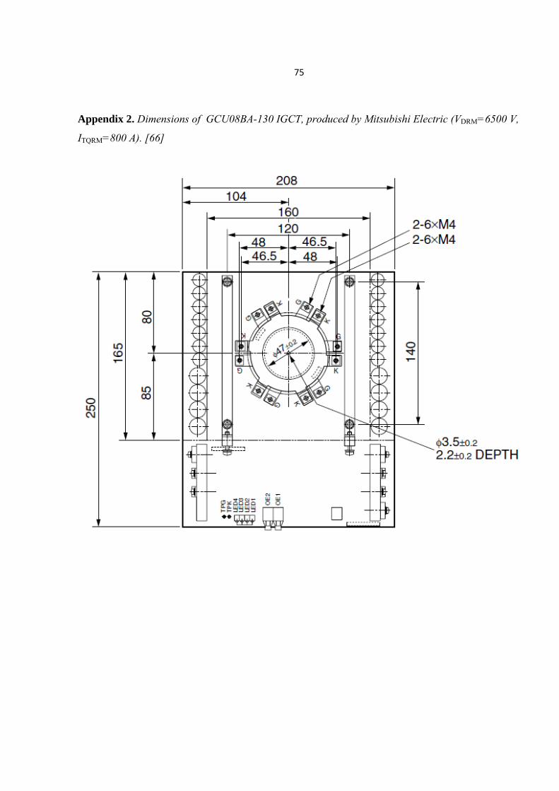
75
Appendix 2. Dimensions of GCU08BA-130 IGCT, produced by Mitsubishi Electric (VDRM=6500 V,
ITQRM=800 A). [66]