tejaswy hari in partial fulfillment of the requirements
TRANSCRIPT

PHYSICAL LAYER DESIGN AND ANALYSIS OF WINLAB NETWORK CENTRIC
COGNITIVE RADIO
by
TEJASWY HARI
A Thesis submitted to the
Graduate School-New Brunswick
Rutgers, The State University of New Jersey
In partial fulfillment of the requirements
For the degree of
Master of Science
Graduate Program in Electrical and Computer Engineering
Written under the direction of
Prof. Narayan Mandayam
And approved by
________________________
________________________
________________________
________________________
New Brunswick, New Jersey
October, 2009

2009
Tejaswy Hari
ALL RIGHTS RESERVED

ii
ABSTRACT OF THE THESIS
Physical Layer Design and Analysis of the WINLAB Ne twork
Centric Cognitive Radio
By Tejaswy Hari
Thesis Director: Prof. Narayan Mandayam
The wireless domain is ever expanding with new technologies and protocols emerging for
all possible environments. Each new protocol is an improvement over the other. High
performance FPGAs have entered the market with advanced signal processing
capabilities which have vast resources and area to accommodate complex designs. The
amalgamation of the two has given rise to programmable radios better known as
cognitive radios. This thesis proposes the physical layer design and analysis of the
WiNC2R- WINLAB Network Centric Cognitive Radio which is a SoC (System on Chip)
based hardware platform on FPGA. This system is based on the Virtual Flow Paradigm.
The key characteristic of this concept is that the protocol processing and selecting
specific hardware accelerators is engaged dynamically by the software.
The WiNC2R consists of three main parts – the data layer, the interconnect layer and the
control layer. All the data processing and functioning is handled by the data layer which
is the focus of this thesis.

iii
We have designed an adaptive modulator and demodulator for WiNC2R. These blocks
exploit the advantages of software flexibility and hardware high speeds. It’s an inter-
protocol operable processing engine that caters to all modulation schemes and can vary
them on the fly. These engines show MIMO capabilities also due to their data flow
independent design. The software interface to the register maps instantiated inside the
processing engines which is used to configure the system before start of the frame.
We successfully sent OFDM frames implemented on Virtual Flow Paradigm across and
performed timing and utilization analysis. The modulator and demodulator parameters
can be conveniently setup in the software. The flexible hardware design enables fast
switching between WiFi and WiMAX frames. The thesis starts with the design of top
level architecture and further dig deeper the design of the Modulator and Demodulator
processing engines. We then conclude with the timing and area resource analysis and
discuss an improvement in design.

iv
Acknowledgements
I would first like to thank my parents and family whose constant support and motivation
has helped me throughout this journey. I would like to thank my advisors Prof. Narayan
Mandayam for his constant guidance and help. I would like to thank Prof. Zoran Miljanic
and Prof. Predrag Spasojevic for instilling a vision for this project and guiding me
through the process. They have dedicated their valuable time and helped me complete my
thesis. I am also indebted to my three most valuable mentors – Khanh Le, Renu
Rajnarayan and Ivan Seskar. Their advice and never ending support has helped me gather
the necessary expertise required to contribute to the team.
I would also like to thank the entire WiNC2R team – Sumit, Shalini, Vijyant, Madhura,
Vaidehi, Akshay, Prasanthi, Mohit and Onkar. They taught me how dedicated team work
can build monuments. I am grateful to be a part of this team. I also thank my friends for
their support. And finally I would thank the staff at WINLAB for providing the facilities
and support required for this thesis.

v
Table of Contents
Acknowledgements ............................................................................................................ iv
Lists of tables ..................................................................................................................... ix
List of illustrations ............................................................................................................. xi
Chapter 1: Introduction ................................................................................................... 1
1.1: Programmable Radios ............................................................................................. 2
1.1.1: USRP ................................................................................................................. 2
1.1.2: USRP 2 ............................................................................................................... 5
1.1.3: WARP ............................................................................................................... 6
1.2: WINLAB Network Centric Cognitive Radio – WiNC2R ........................................ 9
1.3: Virtual Flow Paradigm ............................................................................................. 9
1.3 Contribution ............................................................................................................. 14
Chapter 2: WiNC2R – Top level Architecture ............................................................. 16
2.1: Innovative Integration’s X5-400M board ............................................................... 16
2.2: Steps for implementing on FPGA .......................................................................... 22
Chapter 3: WiNC2R Top Level Architecture ............................................................... 24
3.1: Central Processors - Microblaze ............................................................................. 25
3.2: Processor Logic Bus v46 BUS ............................................................................... 26

vi
3.3: Transmitter Architecture ........................................................................................ 28
3.2 Receiver Architecture .............................................................................................. 29
3.3: System Flow ........................................................................................................... 31
3.3.1: Transmitter Flow for OFDM ............................................................................ 31
3.3.2: Receiver Flow for OFDM ................................................................................ 33
Chapter 4: Functional Unit Architecture ...................................................................... 36
4.1: Bus Interface ........................................................................................................... 37
4.2: Unit Control Module Wrap ................................................................................... 37
4.2.1: UCM ................................................................................................................. 37
4.2.2: Buffers .............................................................................................................. 38
4.2.3: Task Descriptor (TD) Table ............................................................................. 39
4.2.4: GTT Table ........................................................................................................ 40
4.2.5: Task Scheduler Queue...................................................................................... 40
4.2.6: Register Maps................................................................................................... 41
4.2.7: Arbiters ............................................................................................................. 41
4.2.8: DMA Engine .................................................................................................... 41
4.2.9: Processing Engine ............................................................................................ 42
Chapter 5: Processing Engine (PE)............................................................................... 43
5.1: PE Modulator.......................................................................................................... 45

vii
5.1.1: Input Interface .................................................................................................. 45
5.1.2: Processing Engine ............................................................................................ 46
5.1.3: Output Interface ............................................................................................... 51
5.2: PE – Demodulator and Checker ............................................................................. 51
5.2.1: PE Demodulator ............................................................................................... 52
5.2.2: PE Checker ....................................................................................................... 57
5.3: PE Testbench .......................................................................................................... 61
5.3.1: Device under Test ............................................................................................ 62
5.3.2: Reference Text Files ........................................................................................ 62
5.3.3: Testbench Components .................................................................................... 66
Chapter 6: PE Register Maps and Software ................................................................. 68
6.1: Register Map .......................................................................................................... 68
6.2: Address Allocation ................................................................................................ 74
6.3: Software on WiNC2R............................................................................................ 75
Chapter 7: Resource Utilization and Timing ................................................................ 78
7.1: FPGA Resource Utilization .................................................................................... 78
7.1.1: Transmitter Utilization ..................................................................................... 78
7.1.2: Receiver Utilization ......................................................................................... 79
7.2: Timing Analysis ..................................................................................................... 80

viii
7.3: Parallel Implementation Design and Analysis ....................................................... 83
Chapter 8: Conclusion .................................................................................................. 90
References ......................................................................................................................... 93
Abbreviations .................................................................................................................... 94

ix
Lists of tables
Table 1.1: Details of FPGA on USRP – Altera Cyclone EP1C12 ...................................... 3
Table 1.2: Details of FPGA on WARP – Xilinx Virtex2 Pro XC2VP70 ........................... 8
Table 2.1: Details of Virtex5 FPGA ................................................................................. 22
Table 5.1: PE Modulator Command Parameter ................................................................ 47
Table 5.2: Mapping Table ................................................................................................. 50
Table 5.3: PE DmodChkr Command Parameters ............................................................. 54
Table 5.4: Chunk Sizes for WiFi ...................................................................................... 60
Table 6.1: Normalization factors for various modulation schemes .................................. 71
Table 6.2: Modulator Status Register ............................................................................... 72
Table 6.3: Demodulator Checker Status Register ............................................................. 73
Table 6.4: PE RAMs Address Offsets .............................................................................. 75
Table 7.1: Transmitter Utilization..................................................................................... 79
Table 7.2: Receiver Utilization ......................................................................................... 80
Table 7.3: Modulation Latency ......................................................................................... 81
Table 7.4: Latency w.r.t OFDM symbols ......................................................................... 82
Table 7.5: PE Demodulator and Checker Latency............................................................ 82
Table 7.6: Demod. Latency w.r.t OFDM Symbols ........................................................... 82
Table 7.7: Total PE Latency ............................................................................................. 83
Table 7.8: Latency Reduction in Modulator ..................................................................... 85
Table 7.9: Latency Reduction in Demodulator ................................................................. 88
Table 7.10: Parallel Modulator Area Utilization .............................................................. 88

x
Table 7.11: Parallel Demodulator Area Utilization .......................................................... 88

xi
List of illustrations
Figure 1.1: USRP Block Diagram[4] .................................................................................. 5
Figure 1.2: WARP Top Level Architecture[5] ................................................................... 7
Figure 1.3: ADC/DAC interface blocks of WARP[5] ........................................................ 8
Figure 1.4: Hardware and Virtual Pipelining [9] .............................................................. 11
Figure 1.5: Software in WiNC2R ..................................................................................... 12
Figure 1.6: Hardware Platform Comparison[3] ................................................................ 13
Figure 2.1: X5-400M Top Level Architecture[8] ............................................................. 17
Figure 3.1: NCP top level architecture ............................................................................. 24
Figure 3.2: Transmiter Architecture ................................................................................. 28
Figure 3.3: Receiver Architecture ..................................................................................... 30
Figure 3.4: Transmit Control Flow ................................................................................... 32
Figure 3.5: Receiver Command Flow ............................................................................... 33
Figure 4.1: Functional Unit Architecture .......................................................................... 36
Figure 4.2: Buffer Partition ............................................................................................... 38
Figure 5.1: Processing Engine Top Level Diagram .......................................................... 44
Figure 5.2: PE Modulator ................................................................................................. 45
Figure 5.3: Complex Number Representation .................................................................. 50
Figure 5.4: PE Demodulator and Checker ........................................................................ 52
Figure 5.5: Demodulator Output RAM ............................................................................. 56
Figure 5.6: PE Checker ..................................................................................................... 58
Figure 5.7: PLCP Header Contents[15] ............................................................................ 58

xii
Figure 5.8: PE Test Bench Top Level Architecture .......................................................... 62
Figure 6.1: PE Mod Register Maps................................................................................... 68
Figure 6.2: 802.11a constellation diagram ........................................................................ 70
Figure 7.1: Modulation Latency Graph ............................................................................ 81
Figure 7.2: Demod. Latency for various frames ............................................................... 83
Figure 7.3: Modulator Timing Diagram ........................................................................... 84
Figure 7.4: Parallel Modulator Implementation ................................................................ 85
Figure 7.5: Demodulator Timing Diagram ....................................................................... 86
Figure 7.6: Parallel Demodulator Implementation ........................................................... 87

1
Chapter 1:
Introduction
The exponential growth of the wireless industry is clear and evident in all aspects. Cell
phones are now coming equipped with all protocol operability, wireless speeds are slowly
surpassing the wired and remote areas are no longer remote. This has been possible with
developments in physical and MAC layer research, exploding progress in semiconductor
industry and blooming of various languages and scripting tools. The advent of cognitive
radios- radios that can change transmission and receiving parameters based on the
environment is further evidence. These platforms possess inter-operability and efficient
spectrum usage and fast data rates are their main objectives. They will require flexible
physical and complex network layer processing and agility.
Such platforms have not yet entered the commercial market; they are still in the research
phase. The WINLAB Network Centric Cognitive Radio is such a platform that promises
both speed and flexibility in the multilayer domain of mobile multimedia IP based
communication. Its goal is to provide a scalable and adaptive radio platform hence the
design is SoC oriented and FPGA based. The WiNC2R is an excellent platform for the
research domain for analysis of the mobile applications computing, communication and
control requirements, performance analysis of the applications, hardware vs. software
implementation tradeoff analysis. It will also be useful for understanding the potential
and limitations of traditional CPU architecture in addressing the needs of the emerging

2
wireless communications in heterogeneous environments. Thus, this platform will not
only provide a wireless testbed for academia but also a smart wireless device for various
applications.
The following section will illustrate few such platforms that have pre-defined functions
that can be programmed by the user.
1.1: Programmable Radios
1.1.1: USRP
The Universal Software Radio Peripheral is the hardware interface between RF and GNU
software. It is built for general purpose computers to function as high bandwidth software
radios. It works in baseband frequencies.
The advantage of using USRP is that all the signal processing is done in software, thus
avoiding complex HDL language code. GNU uses python code to perform all processing
engine functions. The high speed operations like digital up and down conversion,
decimation and interpolation are done on the FPGA.
The users can develop a wide range of signal processing codes without worrying about
the hardware capability and resources. The powerful combination of flexible hardware,
open-source software and a community of experienced users make it the ideal platform
for your software radio development.
Details of USRP hardware boards [4]

3
• 4 high-speed analog to digital converters (ADCs), each at 12 bits per sample,
64MSamples/sec.
• 4 high-speed digital to analog converters (DACs), each at 14 bits per sample,
128MSamples/sec.
• Altera Cyclone EP1C12 FPGA
• FPGA connects to a USB2 interface chip, the Cypress FX2, and the computer.
• The FPGA connects to a USB2 interface chip, the Cypress FX2. The FPGA
circuitry and USB Microcontroller is programmable over the USB2 bus.
The FPGA used is the Altera Cyclone EP1C12 FPGA whose details are given below. [6]
Feature EP1C12
LEs 12,060
RAM Blocks - M4K 52
Total RAM bits 92,160
PLLs 2
Max user I/O pins 249
Differential Channels 103
Temperature -40°C to +125°C
Table 1.1: Details of FPGA on USRP – Altera Cyclone EP1C12
As mentioned before, FPGA programming is used to interface the ADC and DAC IO
ports to the data-out from the USB. The configuration typically includes digital down
converters (DDC) implemented with 4 stages cascaded integrator-comb (CIC) filters.

4
CIC filters are very high-performance filters using only adders and delays. There are
decimators and interpolators so that the data rate adjusts to USB interface or the RF. Each
DDC has two inputs I and Q. These values are interleaved when multiple channels are
used. The USRP block diagram is shown in Figure 1.1 [4]
Software
The software GNU uses is the Linux C++ where the application program interfaces with
USRP. GNUradio provides USRP interface libraries which have to be linked with the
user code. Most of the signal processing is done in C++. Python and SWIG are used to
connect the blocks together and generate a flow. So the data that is output from the
software can be fed directly to the DAC for transmitting.

5
Figure 1.1: USRP Block Diagram[4]
Many complex systems are easily realizable by software radio. Fast processors, ever-
expanding memory and high level programming have made it easy for designers and
researchers in the wireless domain to implement communication systems.
The disadvantages of SDRs are
• Whenever a block or function call is invoked, the flow switches to and fro to the
CPU processor. This drastically increases processing latency.
• USRP also restricts data flow through USB2.0 which is not scalable.
• Expertise in SDRs require proficiency in multiple languages – C++ and Python
for software and HDL for configuring FPGA
1.1.2: USRP 2
The USRP2 is an improvement over the USRP board and it has the following additional
features [4].
• Gigabit Ethernet interface
• 25 MHz of instantaneous RF bandwidth
• Xilinx Spartan 3-2000 FPGA
• Dual 100 MHz 14-bit ADCs
• Dual 400 MHz 16-bit DACs
• 1 MByte of high-speed SRAM
• Locking to an external 10 MHz reference
6
• 1 PPS (pulse per second) input
• Configuration stored on standard SD cards
• The ability to lock multiple systems together for MIMO
• Compatibility with all the same daughterboards as the original USRP
This board has a high performance RF end and a large FPGA. But the data processing
still is implemented in software, this means that the processing speed depends on the
CPU on which the GNU software is implemented. Hence, the data rate is still
bottlenecked at the software.
1.1.3: WARP
WARP is Rice University’s programmable hardware platform. It stands for Wireless
Open Access Research Platform. Xilinx’s Virtex 2 FPGAs provide vast recourses for
hardware programmability. Like USRP, WARP also has four daughterboard slots that
support wide range of input-outputs. It comes with its own programming tools.
The details of the board are given below [5]
• USB and serial port connectivity to PC
• PowerPC 405 Processor
• Rocket IO Trans-receiver
• Xilinx's SystemACE CompactFlash chip for managing the configuration process
of the FPGA. The SystemACE chip acts as an interface between the FPGA and a
standard CompactFlash slot.

7
• 160MS/s 16-bit dual DACs - AD9777
• 65MS/s 14-bit dual-ADC - AD9248
The top level architecture of WARP is shown below :
Figure 1.2: WARP Top Level Architecture[5]
The FPGA contains the user logic. The FPGA can be programmed by using VHDL or
any other HDL. Typically Matlab and simulink is used to create the bit file that gets
loaded into FPGA.
Details of Virtex2 Pro XC2VP70 are given in the table below [6]
Feature XC2VP70
Rocket IO Trans-Receiver Blocks 20
Power PC Processor blocks 2
Logic Cells 74,448
CLB
8
Slices 33,088
Max distribution RAMs 1,034
Multiplier Blocks 18x18 328
BRAM
18Kb Blocks 328
Max Block RAMs 5,094
DCM 8
Max user I/O Pins 996
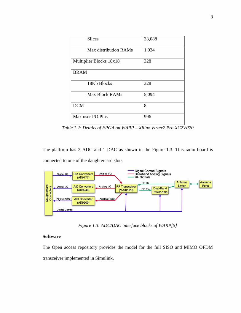
Table 1.2: Details of FPGA on WARP – Xilinx Virtex2 Pro XC2VP70
The platform has 2 ADC and 1 DAC as shown in the Figure 1.3. This radio board is
connected to one of the daughtercard slots.
Figure 1.3: ADC/DAC interface blocks of WARP[5]
Software
The Open access repository provides the model for the full SISO and MIMO OFDM
transceiver implemented in Simulink.

9
The processor used is PowerPC linked to On-chip Peripheral Bus (OPB). OPB is a
synchronous bus that provides separate 32bit addresses and data paths. The data read and
write are implemented with multiplexers. The System Generator tool is responsible for
converting the Matlab code & Simulink blocks to VHDL. The blocks are first created and
linked in Simulink. Once the design is ready, System Generator is invoked and it
performs synthesis and place and route. This design is then loaded to the FPGA.
Disadvantages of WARP
• Limitations to the FPGA resource space compared to the vastness of software
radio resources.
• Limitations to Communication blocks in MATLAB’s Xilinx blockset
1.2: WINLAB Network Centric Cognitive Radio – WiNC2 R
WiNC2R is a network centric cognitive radio developed at WINLAB, Rutgers
University. WiNC2R is a proof of concept design that implements the Virtual Flow
Paradigm (VFP) on FPGA. It is a programmable wireless protocol processing hardware
platform. The VFP[1][2] is a new paradigm for programmable communication
processing.
1.3: Virtual Flow Paradigm
The approach here is to strike a balance between software and hardware. An entire
hardware implementation does not promise scalability and dynamic future evolution.

10
Since such a system does not have enough or any flexibility it fails to process various
communication protocols different from the ones that the hardware is designed for.
The previous section talked about software defined radios that provide high flexibility
and significant interoperability among protocols. But the software latency makes such
systems impractical for high speed designs.
The idea here is to strike a balance between hardware and software implementation. The
virtual flow paradigm solves the problem [1]. This paradigm introduces the Virtual Flow
pipelining (VFP) combines the high speed computation capabilities of FPGA hardware
and flexibility of software. The data flow and parameter inputs to processing blocks are
fed by the user in the form of function calls, but the processing happens on hardware.
This type of flow gives us the freedom to add or remove any functional blocks (FU) or
data processors (DP) dynamically. The blocks are not physically cascaded together which
means they function independent of their preceding or succeeding processors. Hence
there is a requirement of a top controller in these blocks that sets up the flow for every
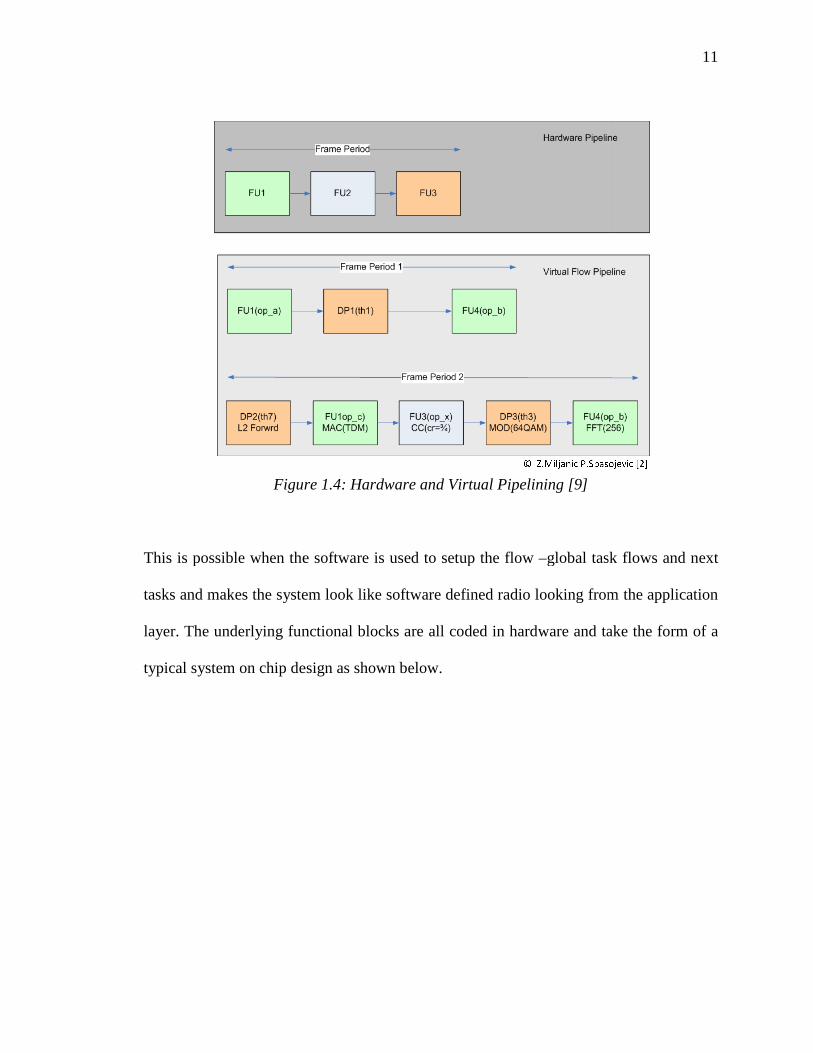
session. As shown in the figure below, the hardware pipeline is a pre-decided hard-coded
flow that cannot be easily modified. This makes it infeasible for cognitive purposes. The
virtual flow pipeline provides room for other blocks to fit in a flow. For eg, the first
frame uses the modules FU1, DP1 and FU4 sequentially. The flow for the next frame
shown is completely changed and independent of the first one.
Figure
This is possible when the software is used to setup the flow
tasks and makes the system look like
layer. The underlying functional blocks are all coded in hardware and take the form of a
typical system on chip design as shown below.
Figure 1.4: Hardware and Virtual Pipelining [9]
This is possible when the software is used to setup the flow –global task flows and next
tasks and makes the system look like software defined radio looking from
layer. The underlying functional blocks are all coded in hardware and take the form of a
typical system on chip design as shown below.
11
global task flows and next
from the application
layer. The underlying functional blocks are all coded in hardware and take the form of a

12
Figure 1.5: Software in WiNC2R
The figure above shows such a scenario where the MAC Tx and Modulator are the
functional blocks. Ever Functional Unit (FU) has control units in them that interpret the
software calls. The next-task processors forward the processed data from the producer to
the consumer based on a task table that is setup by the user via software.
The WINLAB Cognitive Radio Platform WiNC2R is proposed and designed with the
objective of achieving at speed processing of emerging WLAN and wireless broadband
protocols with flexible architecture. Its underlying flexibility allows evolution within its
domain space through software upgrades, and measurements and collaboration in the
field with waveform and protocol adjustments for the optimum spectrum utilization. With

the help of the VFP, it places itself between high speed designs and highly programmable
platforms as shown in the
WiNC2R on FPGA is well balanced in terms of programmability and speed. The figure
also shows that the ASIC implementation will further improve the platform and promise
greater speeds. The area of the rectangle
number of gates.
VANU
GNU/USRP
Programmabilty
Figure
Since FPGA is resource limited, we cannot achieve speeds greater than 50Mbps. We will
require multiple FPGAs interfaced on PCI Express cards to achieve larger speeds. This
project targets ASIC production to reach the 100Mbps destina
, it places itself between high speed designs and highly programmable
platforms as shown in the Figure 1.6.
WiNC2R on FPGA is well balanced in terms of programmability and speed. The figure
also shows that the ASIC implementation will further improve the platform and promise
greater speeds. The area of the rectangle corresponds to the complexity of design
WinCASIC
performance
Complexity # of gates ~ area of rectangle
VANU
WARP
PicoChip
100
WinC2RFPGA
50 Mbps
Figure 1.6: Hardware Platform Comparison[3]
Since FPGA is resource limited, we cannot achieve speeds greater than 50Mbps. We will
require multiple FPGAs interfaced on PCI Express cards to achieve larger speeds. This
project targets ASIC production to reach the 100Mbps destination. The WiNC2R on
13
, it places itself between high speed designs and highly programmable
WiNC2R on FPGA is well balanced in terms of programmability and speed. The figure
also shows that the ASIC implementation will further improve the platform and promise
the complexity of design or the
WinC2RASIC
performance
area of rectangle
100 Mbps
Since FPGA is resource limited, we cannot achieve speeds greater than 50Mbps. We will
require multiple FPGAs interfaced on PCI Express cards to achieve larger speeds. This
tion. The WiNC2R on

14
FPGA is merely a proof-of-concept implementation and the design procedure is followed
to demonstrate the working of the Virtual Flow Paradigm. The modules are not optimized
with respect to resources for commercial use.
1.3 Contribution
The thesis explores the top level design of the WiNC2R. It describes the Virtual Flow
Paradigm implementation on FPGA and the modules used to achieve virtual flows. The
focus of this thesis is the design and analysis of physical layer blocks on the WiNC2R.
The modulator and demodulator have been designed to cater to the virtual flow paradigm.
These blocks implement adaptive modulation. The user can setup the constellation points
prior to the transmission. Further, during runtime, each chunk of frame, WiFi or
WiMAX, can be modulated by any 4 types of modulations. It can be further noted that
the processing engines work independent of each other. Hence, MIMO transmissions are
possible.
The blocks have also undergone vigorous testing with the help of a simulated MATLAB
model and the Bus Functional Module (BFM) environment. After successful
transmissions of frames of various sizes and modulation schemes, the WiNC2R was
programmed on to the FPGA.
Timing analysis and resource analysis has been performed to determine the processing
latency. Even with high programmability, high speeds are achievable because the
flexibility is implemented in hardware. The timing analysis establishes how much latency

15
is contributed by the processing engines to the entire flow. The analysis also provides
FPGA area utilization which will be useful for future WiNC2R releases.
The following section will explain the top level architecture.

16
Chapter 2:
WiNC2R – Top level Architecture
2.1: Innovative Integration’s X5-400M board
WiNC2R is implemented on Innovation Integration’s X5-400M board. This section talks
about the top architecture design and the interface blocks instantiated in it. The X5-400M
is PCI Express Mezzanine Card (XMC) IO module having the following features [7]
• Two 14-bit, 400 MSPS A/D and two 16-bit, 500 MSPS DAC channels
• Virtex5 FPGA - SX95T
• PCI Express host interface with 8 lanes
• 1 GB DDR2 DRAM
• 4MB QDR-II
The figure below gives us the top level diagram. The board has various IO interfaces that
are mentioned above and all the interfaces are designed and implemented on VHDL.
WiNC2R uses some of these blocks based on the requirement. The blocks were provided
by Innovative Integration board.

17
©Innovative Integration [8]
Figure 2.1: X5-400M Top Level Architecture[8]
2.1.1) PCIe interface – PCI express 8 lanes
The PCIE interface block (ii_pcie_intf) provides a streaming, control and status interface
to the host PCI Express interface for the user logic. It provides 8 lane motherboard-level
interconnectivity and its scalable shared parallel bus architecture caters to high speed data
and control transfers. It is also used to reprogram the FLASH memory on FPGA. FLASH
memory is a reprogrammable memory that uses only a single power supply, making it
ideally suited for in-system programming. The flash memory is used to store the

18
application software. This block also monitors the FPGA temperature. If the temperature
exceeds 85°C, this block triggers alerts and warnings. Modules use these indicators to
spawn cooling and shut-down tasks.
2.1.2) RapidIO Interface
The Xilinx RapidIO is a 3 layer endpoint solution which allows the users to integrate
necessary portions of the design. It comes with its own protocols and frame structures.
The interface block (ii_dio) provides a simple modifiable interface with registers between
the user logic and RapidIO for memory read and write.
This module is not instantiated in WiNC2R because RapidIO is not used.
2.1.3) DRAM Controller
The ii_128mq component has a high performance DDR2 DRAM interface and that
requires constrained routing to the microblaze processor on the FPGA. It is connected to
the Multi-Port Memory Controller (MPMC) in microblaze that supports SDRAM (single
data RAM) , DDR/DDR2 (Dual Data Rate) memory. Typically, it has an address and
Data Paths, Arbiters for access control, a configurable physical interface IDELAY
controller, Clock and Reset Logic.
This interface is used to load the application software. It as used as a replacement to
Flash memory due to its huge capacity to load application software. Details of this block
will be mentioned in the Software section of this document.

19
2.1.4) QDR SRAM Controller
This component (ii_qdr_sram) provides an interface from the user logic to quad data
rate(QDR) synchronous burst SRAM memories. The interface component supports the
dual data path architecture of QDR SRAM by providing dual 18-bit address buses for
read and write addressing, dual 32-bit data paths for read and write from the SRAM
device. SRAMs are not used by WiNC2R, hence this module is also not used. The top
level IO pins are terminated as per the user-guide.
2.1.5) DAC
The DAC5687 is used in the WiNC2R. It has a 16-bit high speed DAC with
interpolation filters with 2x,4x and 8x capability. It also has on board Numerically
Controlled Oscillator (NCO) and onboard clock multiplier.
The X5-400M board consists of various blocks that process the data and make it
compatible to the DAC. The blocks are instantiated in a block called ii_dac_intf. The dac
interface block is instantiated between the user logic output and the DAC chip on the
board. It works with 16 bit data on the system clock.
• The input to this block comes from the user logic design – WiNC2R physical
layer. The data is 16 bits and two modules are instantiated for I and Q values. The
enable is always set high and DAC is always switched ON since frame detection
happens at the receiver. This end works on system clock.
• The data is then forwarded to an offset and gain block (ii_offgain). This block
compensated for gain and offset errors. These values can be set by the user
20
through the software. There are specific memory locations for these values on
which the user can write and read.
• After the error corrections are made, the data flows into a 1K, 16in-16out FIFO.
The FIFO is written on system clock but it outputs on the sample clock
(dac_plllock) which can be set using the interpolation coefficient. This FIFO has
alarms and flags if the buffer overflows or underflows.
• This interface is also equipped with test generators. By enabling the test
generator, the module outputs a sample sine or ramp wave based on the amplitude
and frequency offset set by the user.
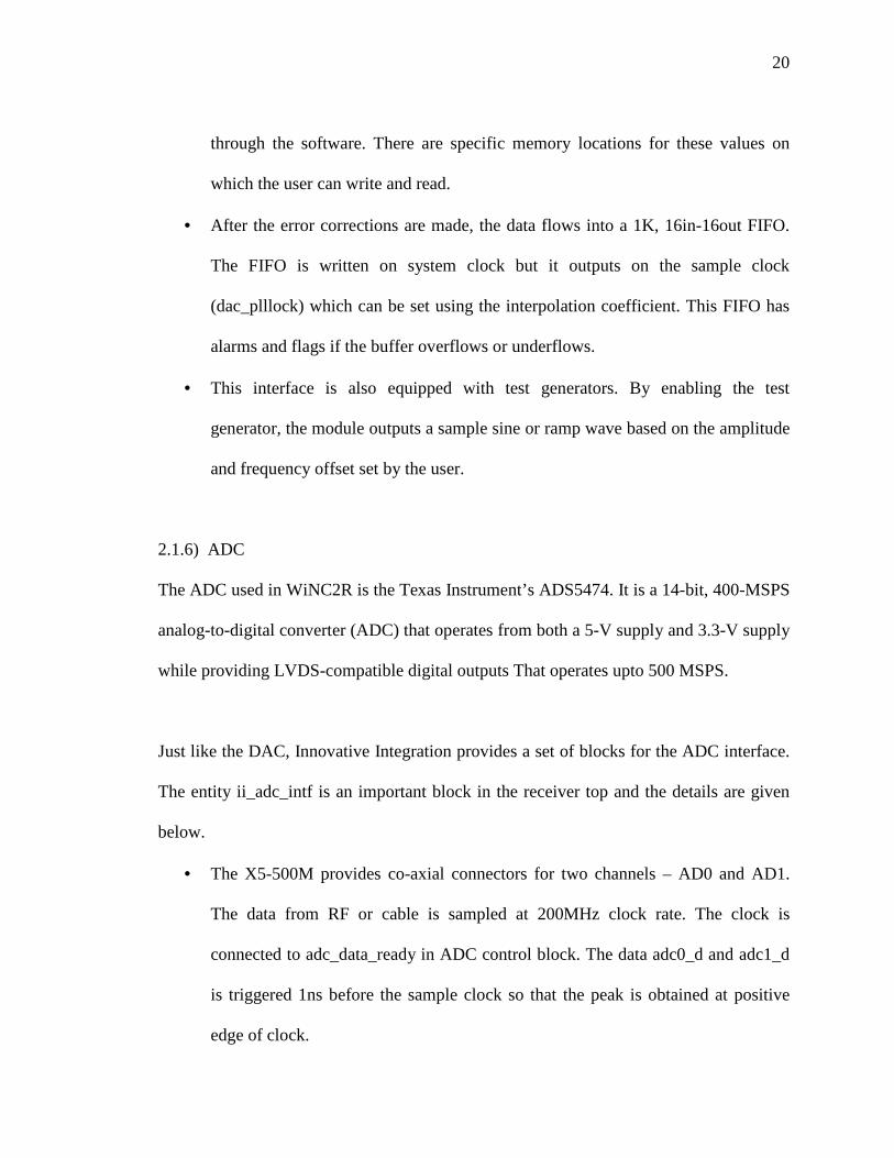
2.1.6) ADC
The ADC used in WiNC2R is the Texas Instrument’s ADS5474. It is a 14-bit, 400-MSPS
analog-to-digital converter (ADC) that operates from both a 5-V supply and 3.3-V supply
while providing LVDS-compatible digital outputs That operates upto 500 MSPS.
Just like the DAC, Innovative Integration provides a set of blocks for the ADC interface.
The entity ii_adc_intf is an important block in the receiver top and the details are given
below.
• The X5-500M provides co-axial connectors for two channels – AD0 and AD1.
The data from RF or cable is sampled at 200MHz clock rate. The clock is
connected to adc_data_ready in ADC control block. The data adc0_d and adc1_d
is triggered 1ns before the sample clock so that the peak is obtained at positive
edge of clock.

21
• The adc0 and adc1 data flow into the adc control block and get combined into 32
bit words. The I and Q values are clubbed together and made compatible to the
WiNC2R protocol followed.
• The 32 bit words are written to a 1K 32in-32out FIFO where the write enables
follow the sample clock. The reading happens at the system clock. The
decimation coefficient is set up by the user. The adc_intf reads the decimation
value from a designated address location to which the user has access to. It is
default set to 4.
• The output from the adf_intf is sent to the processing engine of the receiver.
• The gain and the offset can also be set by software. User can change these values
dynamically by writing into the addresses assigned.
2.1.7) Application FPGA
Since all the signal processing is left to the FPGA, we use a large area FPGA. Virtex5
FPGA - SX95T is best suited for this application. It has a large number of DSP blocks
and RAMs to fit in the entire transmitter or receiver.
The details of FPGA are:
Feature SX95T
Rocket IO Trans-Receiver Blocks 16
CMT 6
Ethernet MACs 4

22
Endpoints Blocks for PCIe 1
CLB
Array (RowXCol) 160 x 46
Slices 14,720
Max Distr RAM (Kb) 1,520
DSP48E 640
BRAM
18Kb Blocks 488
36Kb Blocks 244
Max Block RAMs 8,874
Total I/O Banks 19
Max user I/O Pins 640
Table 2.1: Details of Virtex5 FPGA
2.2: Steps for implementing on FPGA
a. Architecture Design and documentation.
b. The RTL design is in VHDL
c. Simulation in Mentor Graphics Modelsim and Functional Verification using
Matlab and Bus Functional Model (BFM).
d. Synthesis - A process that converts high-level abstraction to low-level. The
VHDL code is converted to gate level implementation for FPGA. The tool used is
Mentor Graphics - Precision RTL Synthesis.
23
e. Xflow - Xilinx tool to achieve a design flow.
f. Place and Route – This step places the logic elements generated after synthesis on
FPGA and interconnects them on FPGA. It is a long process where the Xilinx tool
optimizes the space and routing to meet the timing constraints.
g. The step generates a bitfile which is loaded into the FPGA using Xilinx Impact.
h. Xilinx also provides a software development kit with Xilinx libraries to generate
the software image that is loaded in the BRAM. We can access all memory
locations through the software.

24
Chapter 3:
WiNC2R Top Level Architecture
This section will explain the WiNC2R top architecture that is implemented on FPGA.
The systems top level architecture is called ncp_top and it instantiates the main
architecture ncp_cmn and the IO buffers [9].
©WiNC2R
Figure 3.1: NCP top level architecture
Syntheses provides an option of automated Input-Output buffers (IOBUFs) instantiation
where the tool recognizes the IO ports and places the corresponding buffer before it.
Also, when the microblaze processor is built, the tool internally places an IOBUFs for the
DRAM interfaces. The place and route tool then flags an error due to the contention of

25
multiple buffer instantiation. Hence, we manually insert the buffers where needed in the
top file to isolate the central architecture and the buffers.
The WiNC2R architecture sits in the entity ncp_top_cmn. There are three main parts in
this architecture [9]
• Microblaze – Central Processor
• Functional Units – Signal Processing Units
• X5-400M Interface Units – ADC/DAC interfaces
3.1: Central Processors - Microblaze
The MicroBlaze embedded processor soft core is a reduced instruction set computer
(RISC) optimized for implementation in Xilinx Field Programmable Gate Arrays
(FPGAs). It is implemented with a Harvard memory architecture; instruction and data
accesses are done in separate address spaces. Each address space has a 32-bit range (for
example, handles up to 4-Gb of instructions and data memory respectively). The
instruction and data memory ranges can be made to overlap by mapping them both to the
same physical memory. This is useful for software debugging. Figure 3.1 shows the
functional block diagram of the Microblaze core[6].
Microblaze has the following features:
• Thirty-two 32-bit general purpose registers,

26
• Up to eighteen 32-bit special purpose registers, depending on the configured
options,
• 32-bit instruction word with three operands and two addressing modes,
• 32-bit address bus,
• Single issue pipeline,
• Three interfaces for memory accesses - Local Memory Bus (LMB),Processor
Local Bus (PLB) or On-Chip Peripheral Bus (OPB),Xilinx Cache Link (XCL)
• Supports reset, interrupt, user exception, break, and hardware exceptions,
• Supports optional direct mapped Instruction and Data cache for improved
performance,
• Floating Point Units based on IEEE 754 single precision floating point format,
• Fast Simplex Link (FSL) that provides a low latency dedicated interface to the
processor pipeline, extending the processors execution unit with custom hardware
accelerators,
• Debug interface connected to the Xilinx Microprocessor Debug Module (MDM)
core, which interfaces with the JTAG port of Xilinx FPGAs
3.2: Processor Logic Bus v46 BUS
The PLB is a synchronous, high performance bus used to inter connect high performance
processor, ASIC and memory cores. It provides the infrastructure for connecting an
optional number of PLB masters and slaves into an overall PLB system. It consists of a

27
bus control unit, a watchdog timer, and separate address, write, and read data path units.
The main features of the PLB bus are [6]:
• PLB arbitration support for up to 16 masters with number of PLB masters
configurable via design parameters.
• PLB address and data steering support for up to 16 masters128-bit, 64-bit, and 32-
bit support for masters and slaves
• PLB address pipelining
• Four levels of dynamic master request priority
• PLB Reset generated synchronously to the PLB clock from external reset when
external reset provided
• DMA support for buffered, peripheral-to-memory, memory-to-peripheral, and
memory to memory transfers

28
3.3: Transmitter Architecture
The working force of the system is the team of Functional Units (FU). The transmitter
blocks are the MAC Tx, Header, Modulator and IFFT. The output of the FFT is
connected to the DAC interface block. For the transmitter case, only these FUs and the
DAC interfaces are instantiated.
Processor Core
FU MAC TX
FU HDR
FU MOD
FU IFFT
Microblaze PLBv46 BUS LMBv10
BRAMBRAM I/F Contr
XPS_uartlite XPS_gpio XPS_intc
xps_mch_emc mpmc ipif_final
Bus Interface
Unit Control Module Wrapper
Processing Engine
fpga_0_RS232_RX_pin fpga_0_RS232_TX_pin sys_clk_pin sys_rst_pinxps_gpio_0_GPIO_d_out_pinxps_mch_emc_0_Mem_DQ_pinxps_mch_emc_0_Mem_A_pin xps_mch_emc_0_Mem_RPN_pin xps_mch_emc_0_Mem_CEN_pin xps_mch_emc_0_Mem_OEN_pin xps_mch_emc_0_Mem_WEN_pinmpmc_0_DDR_DQSmpmc_0_DDR_DM_pinmpmc_0_DDR_DQmpmc_0_DDR_Addr_pin mpmc_0_DDR_BankAddr_pin mpmc_0_DDR_WE_n_pinmpmc_0_DDR_CAS_n_pinmpmc_0_DDR_RAS_n_pinmpmc_0_DDR_CS_n_pinmpmc_0_DDR_CE_pin mpmc_0_DDR_Clk_n_pinmpmc_0_DDR_Clk_pin global_timer_rst global_timer_tick
ncp_top_tx
I/O B
UF
S
ncp_top_tx_wrap
pcore
Functional Unit
CLK Reset Logic
DAC Trigger
DAC Interface
Block
FU PCIe
Data to DAC
Data
Figure 3.2: Transmiter Architecture

29
The Figure 3.2 depicts an 802.11a-lite transmitter implementing the virtual flow
pipelining to send an OFDM frame. Due to area restrictions, we couldn’t instantiate all
processing blocks of 802.11a. The processor and bus reside in the processor core bus.
There are 4 functional units that are plugged to the bus. They include :
• MAC: The software feeds the MAC with the frame and this block attaches the
required headers as per the standard. This is called 802.11a-lite MAC.
• Header: This block appends the PLCP header before the frame and also pads
zeros at the end of the frame to make the frame size an integral multiple of
number of OFDM symbols
• Modulator: The frame is then modulated according to the modulation shceme
decided by the software.
• IFFT: The output of the modulator goes through IFFT and filters.
The content at the output of the FFT are OFDM format and are passed on to the DAC.
The DAC interface block is also connected to the bus, hence the configuration parameters
can also be setup by the user.
3.2 Receiver Architecture

30
The receiver structure is similar to the transmitter. Only change is that the Functional
units cater to receiver now. The ADC interface connects to the Synchronizer FU. The
DAC interfaces don’t get connected and the pins are terminated. The receiver
implementation diagram is shown the figure 3.3.
Processor Core
FU MAC RX
FUDMOD
FUCHKR
FUSYNC
Microblaze PLBv46 BUS LMBv10
BRAMBRAM I/F Contr
XPS_uartlite XPS_gpio XPS_intc
xps_mch_emc mpmc ipif_final
Bus Interface
Unit Control Module Wrapper
Processing Engine
fpga_0_RS232_RX_pin fpga_0_RS232_TX_pin sys_clk_pin sys_rst_pinxps_gpio_0_GPIO_d_out_pinxps_mch_emc_0_Mem_DQ_pinxps_mch_emc_0_Mem_A_pin xps_mch_emc_0_Mem_RPN_pin xps_mch_emc_0_Mem_CEN_pin xps_mch_emc_0_Mem_OEN_pin xps_mch_emc_0_Mem_WEN_pinmpmc_0_DDR_DQSmpmc_0_DDR_DM_pinmpmc_0_DDR_DQmpmc_0_DDR_Addr_pin mpmc_0_DDR_BankAddr_pin mpmc_0_DDR_WE_n_pinmpmc_0_DDR_CAS_n_pinmpmc_0_DDR_RAS_n_pinmpmc_0_DDR_CS_n_pinmpmc_0_DDR_CE_pin mpmc_0_DDR_Clk_n_pinmpmc_0_DDR_Clk_pin global_timer_rst global_timer_tick
ncp_top_rx
I/O B
UF
S
ncp_top_rx_wrap
pcore
Functional Unit
CLK Reset Logic
ADC Ctrl & Trigger
ADC Interface
Block
FU IFFT
Data from ADC
FUPCIe
Data
Figure 3.3: Receiver Architecture
31
The receiver instantiates the following functional units :
• Synchronizer: This block is responsible for frame detection and frequency
correction of the received frame.
• FFT: The received frame passes through FFT.
• Demodulator: This block demodulates the frame based on the modulation scheme
and decision table setup by the user.
• Checker: This block contains the parity checker for the PLCP frame and CRC
checker for the data frame.
• MAC: The checker passes the data to MAC which removes the header and
forwards the frame to the software for verification
The data at the synchronizer is received from the ADC. Just like the DAC, the ADC
parameters can also be configured by the user at runtime.
3.3: System Flow
The data and control flow demonstrated in the WiNC2R demo is that of 802.11a-Lite
ODFM. As mentioned before, the functional units correspond to the basic physical and
MAC layer blocks required for basic frame transmission. The task by task flow, which is
setup by the user, is elaborated in detail below.
3.3.1: Transmitter Flow for OFDM
The transmitted functional units and the command flow of an OFDM transmitter is
shown in the figure below [10].

32
©Renu Rajnarayan
Figure 3.4: Transmit Control Flow
Transmitter Tasks
1. TxDataAvl – The frame, which is written in software, is written into the input
buffer of MacTx block. MAC then spawns this task to the frame header creator
and forwards the frame.
2. TxStartCtrl – This task is sent to the receiver FFT to indicate that the control
message is being transmitted. In this case, the preamble is sent.
3. TxPreambleCtrl – The preamble is sent directly to the IFFT for transmission
during this task.
4. TxEndCtrl – This task is sent to the receiver to indicate end of preamble
transmission.

33
5. TxMod – The modulator identifies this task and proceeds with modulating the
input buffer. There are three different tasks for the first chunk, last chunk and the
intermediate chunk. But the modulation works independent of these sub-tasks.
6. TxIFFT – The mod forwards the data to the input buffer of the IFFT during this
task. This is the final task of one frame cycle. The FFT forwards the content
directly to The DAC.
3.3.2: Receiver Flow for OFDM
The receiver functional units and their command flows are shown in the diagram below
[10].
©Renu Rajnarayan
Figure 3.5: Receiver Command Flow
1. ChannelIdle – When the receiver is idle, it sends channel idle to Mac in the
transmitter. On sensing this, the Mac sends frame across channel.

34
2. RxStartRevCtrl – On receiving this task from the transmitter, the auto-correlator
in the synchronizer scans the channel for valid preambles and extracts the
parameters out of it.
3. ChannelBusyCtrl – Once these parameters cater to a valid OFDM frame, the
receiver locks the channel by sending the busy signal. This is a part of the
medium access control to avoid frame collisions.
4. RxHdrDmod – After the preamble is parsed, the PLCP header (802.11a header) is
demodulated.
5. RxPLCPChk – The frame checker checks the parity of the header and extracts the
frame parameters from it.
6. RxData – Once the header test passes, frame date is requested by the frame
checker. There are three sub-tasks for all the data tasks: first, last and intermediate
chunk.
7. RxDeMod – This task indicates the frame is ready in the demodulator input buffer
to be demodulated.
8. RxFrameChk – The frame checker checks the CRC of the incoming frame
chunkwise and forwards data to the MAC.
9. RxMacData – The frame is checked for validity by the MAC and it interrupts the
software accordingly.
10. ChannelIdle – After the frame is processed by MAC, its sends channel idle on the
channel for future frames.

35
This concludes the conceptual part of the thesis. The coming chapters will illustrate how
this design concept was implemented on FPGA. The document starts with the basic top
level Functional Unit Design and digs into details of every block. The physical layer
blocks – Modulator and Demodulator are discussed in detail along with the testing
methodologies.

36
Chapter 4:
Functional Unit Architecture
The functional unit is the working force of the WiNC2R. They can be viewed as
functions in software developed on hardware. They are connected to the slave interface of
the bus only. They are completely independent of each other hence they can be connected
or disconnected on the fly. All FUs share a common entity structure and architecture.
They differ on the processing engine instantiated in them.
The FU has three modules [11]
• Bus Interfaces - Intellectual Property Interface (IPIF)
• Unit Control Module Wrapper (UCM Wrapper)
• Processing Engine (PE)
The top level architecture diagram is shown below.
©WiNC2R
Figure 4.1: Functional Unit Architecture
37
4.1: Bus Interface
The FU ports must be consistent with the Bus signals. The Intellectual Property Interface
(IPIF) features are
• It provides bidirectional interface between the user logic – UCM & PE and the
PLBv46 bus standard [6].
• It provides access to 32,64 and 128 width bus
• Both master and slave interfaces are merged into one block
• This block is generated using Xilinx Core Generator. The generated code was
modified to isolate the user logic from the bus.
4.2: Unit Control Module Wrap
The UCM wrapper mainly consists of the UCM and blocks required for its access to the
bus. It consists of the management layer of the WiNC2R- above MAC and PHY .
4.2.1: UCM
It is in charge of scheduling the tasks to the unit that it is associated with, assigning the
task, monitoring the task completion, and communicating with the other units in the
system for task sequencing. The task scheduling and sequencing in essence forms Virtual
Flow Pipelining - the sequence of tasks performing the functions of the network protocol
under the strict time frame constraints or with the best effort approach. The Virtual
Channel is the sequence of tasks linked together. The linkage specifies the time frame

38
duration which will constrain the duration of the sequence of tasks within the frame
boundary, as well as repetition period of the tasks in every frame.
4.2.2: Buffers
OutDataPtr0
OutDataSize0
0x0080
0x0084
OutDataPtr1
OutDataSize1
. . .
OutDataPtr15
OutDataSize15
0x00F8
0x00FC
. . .
Data Region 0
Data Region 1
0x0100
FlowContex
Pointer Set Region
Pointers to Data Regions
Error Messaging
OutDataPtr14
OutDataSize14
Pointer to Error Messaging
Pointer to FlowContext
Buffer Region
0x1FFC
DMA Mailbox RegionOutgoing Mailbox
(16-Word)
Incoming Mailbox(16-Word)
0x0000
0x0040
InDataPtr0
InDataSize0
0x0000
0x0004
InDataPtr1
InDataSize1
InDataPtr3
InDataSize3
0x0020
. . .
Buffer 0
Buffer 1
FlowContext
Pointers to active buffers
InDataPtr2
InDataSize2
Buffer Region
0x1FFC
Context Region
Data Pointer Set
Control Pointer Set
©WiNC2R
Figure 4.2: Buffer Partition
Input Buffer Output Buffer

39
The processing engines the input and output buffers that the processing engines use for
data processing. They are 1K 33bit Dual port RAMs generated by Xilinx Core Generator.
The buffers are partitioned into two parts – pointer region and data region.
There are common interface blocks in the processing engine that are aware of these
partitions and write/read into them accordingly. They are the ones that manage the data in
all the regions[11].
• Region 0 in both the buffers contains data.
• Region 1 contains the parameter word. The parameter word contains all the
details of the data that is stored in region 0.
• Region 3 in input buffer and Region 15 in the output buffer are reserved for
context data. Context contains that data that are not a part of the frame that is
being transmitted. If two or more processing engine need to share data that is not
a part of the frame but required for the processing of the frame, they use these
regions.
4.2.3: Task Descriptor (TD) Table
The TD interface contains the Task Descriptor table (TD). This block specifies the task
flow execution within the PE. In this table, the active task and next tasks are specified for
every FU. The UCM fetches the information related to a task belonging to a particular PE
from the TD table of that PE. The user has access to this RAM and can fill in the task
information. The TD table contains the information about the number of input/output
buffers used by the task, the next tasks triggered after the successful execution of that
40
task and the information about whether a task is a chunking/dechunking task or not. This
table can be updated for every task through the software.
4.2.4: GTT Table
The Global Task Table (GTT) is a centralized table that resides in the BRAM connected
to the secondary PLB bus. The processor creates and initializes the GTT at the start. The
PEs decodes the data written into this table for task execution and insert the asynchronous
target (consumer) tasks to the FU's queues. This table gives a global view of the data flow
and it can be set for every frame. The TD table of every PE refers to this table to
determine what its next task is. It also synchronizes task execution with the completion
of all producer tasks.
The UCM in every FU accesses the GTT. It is array indexed by 15 bit TaskID in the Task
Descriptor Table (TD) which is preset. The values in the GTT are modified by the UCM
during the task execution. The GTT contains the information about the different tasks and
which FU the tasks are associated to. It also helps in the task synchronization through the
enable flag processing. It also contains configuration settings for the tasks.
4.2.5: Task Scheduler Queue
When Producer UCM wants to schedule a task, it writes a descriptor which is present in
this block to either Synchronous or Asynchronous Descriptor FIFO. This indicates to
Task Scheduler Queue (TSQ) Controller that a task is ready for the en-queuing process.
This block manages tasks by placing them in queues and pushing them whenever needed.

41
4.2.6: Register Maps
Every FU also has a register map that interfaces to the user. The user can set various
parameters directly which the UCM can access. They include information like task
priorities, interrupt handling, error handling and task scheduling.
4.2.7: Arbiters
Since every block in this wrap has slave access to the bus, arbiters are placed in every
block that grant access whenever the bus is idle. The arbiters work on the Bus2IP_CS or
chip select signal to select the corresponding block.
4.2.8: DMA Engine
The DMA Engine provides the interface to the PLBv46 Master bus. UCM requests for
PLB bus services from the DMA Engine, and provides the byte length, source and
destination addresses information. Once configured, the DMA Engine performs the PLB
bus DMA transactions autonomously. The various transfers handled by the DMA are -
1. Producer Output Buffer -> Consumer Input Buffer (Write transaction)
2. Producer UCM -> Consumer UCM (Write transaction)
3. Producer UCM <- Consumer UCM (Read transaction)
4. Producer UCM -> GTT (Write transaction)
5. Producer UCM <- GTT (Read transaction)
42
4.2.9: Processing Engine
The processing engines are the data processing blocks in the WiNC2R. The main MAC
and PHY layer functioning for OFDM are performed at this level. The interfaces of these
blocks are pre defined and are compatible to the UCM ports and the bus interface. Details
of these blocks are presented in the further chapters.

43
Chapter 5:
Processing Engine (PE)
©WiNC2R

44
Figure 5.1: Processing Engine Top Level Diagram
The figure shows the arrangement of the top level processing engine[10]. The Command
Processor (CP), Frame Delimiter and Generator (FDG) , Task Spawning Processor (TSP)
and Register Maps (RMAP) are the blocks that isolate the processing unit from the upper
level control blocks, they are referred to as ‘PE Common Blocks’. The main objective of
using the common blocks is to standardize PE input/output ports and make them
independent from the UCM and I/O buffers. The function of the common blocks is given
below-
1. Command Processor (CP): It translates the commands coming from the Unit Control
Module (UCM) to single-pulse action signals. Each PE can setup the number of
action signals and context data required.
2. Frame Delimiter and Generator (FDG): The FDG is the interface between processing
unit and the input buffer. The PE requests data for a particular data region and FDG
extracts the data from the input buffer.
3. Task Spawning Processor (TSP): TSP helps the PE write to the output buffer.
Whenever PE wants to write its output to the buffer, it requests TSP with data region.
After TSP acknowledges, it waits for SOF and Enables from PE.
4. Register Maps (RMAP): Every PE maintains a register map that adds as a slave
interface to the PLBv46. The user can access PE only through the register map. User
can write to the control register from software. PE can write status details like error
messages, state etc. to the status register so user can read during board testing. Details
of RMAP can be found in RMAP section of Chapter 6.

45
5.1: PE Modulator
The Modulator Processing Engine (pe_mod) is an adaptive modulator that uses a user-
defined mapping table. Since WiNC2R caters to OFDM frames, the modulator is
designed for the 802.11 and 802.16 constellations provided by the standards. But this
module is not restricted for the standards. A user-defined constellation space can also be
defined and loaded into the modulator through the register map (pe_mod_rmap).
The block diagram and schematic details of the modulator is shown below.
Figure 5.2: PE Modulator
5.1.1: Input Interface

46
CP Interface Commands
The modulator has only one action signal – TxMod that initiates the mapping of the data
chunk. The assertion of this signal indicates that there is a data chunk in the input buffer
and the modulation procedures can begin.
FDG Interface
The PE fetches the parameter word that lies in the region 1 of the input buffer. The 32-bit
word contains the properties of the frame to be received. These parameters cannot be
altered and any change would result in modifications of the VHDL code.
The details of the parameter word are explained in the next section.
5.1.2: Processing Engine
The crux of the modulator is the RAM which contains the mapping table and an address
decoder associated with it. The mapper block extracts the information from the input
buffer and activates the address decoder based on the type of modulation.
Parameter Parsing :
The parameter word bit-mapping is shown below.
Bits Content
b31 Preamble Present
b30 Not End of Burst
b29 - b28 Midamble Interval

47
b27 - b23 Sub-channelization
b22 Short/Long Preamble
b21- b20 Channel ID
b19 No Coder
b18 Uplink/Downlink
b17-b16 Standard ID
b15-b11 Header Bytes
b10-b9 Header Code Rate
b8-b7 Header Frame Modln
b6 Header Present
b5-b4 Code Rate
b3-b2 Frame Modln
b1-b0 Frame Status Bits
Table 5.1: PE Modulator Command Parameter
The properties that are used by the modulator are
1. Frame Tag Bits (b1 b0) : ftag
Indicates which part of the frame the chunk belongs
00 – Start and End of frame
01 – Start of frame
10 – Middle of frame
11 – End of frame
2. Frame Modulation (b3 b2) : fmod
Indicates the type of modulation for frame

48
00 – BPSK
01 – QPSK
10 – 16QAM
11 – 64QAM
3. Code Rate (b5 b4) : frate
Indicates the rate of the frame (If coder present)
00 – ½ code
01 – ¾ code
10 – 2/3 code
11 – 5/6 code
4. Header Present (b6) : Indicates whether PLCP is present in the chunk
5. Header Modulation (b7 b8) : hmod
Indicates the modulation technique for the header
6. Header Code Rate (b10 b9) : hrate
Indicates the rate of header
7. Header Bytes (b15 – b11) : hsize
Contains the number of bytes present in the header
8. Standard ID (b17 – b16) :
00 – WiFi 01 – WiMax

49
The control word contains the parameters for the data present in the data region of the
input buffer. The modulator becomes aware of the frame type – WiFi or WiMAX and the
type of modulation based on this word.
The 802.11 standard’s PLCP header typically is BPSK modulated and ½ coded. If the
coder is not present ½ repetitive code is implemented.
Data Parsing:
Once the modulator is set based on the parameters, we request for the region 0 which
contains of the frame with or without header. If the header is present, the first ‘hsize’
number of bytes are modulated using the hmod scheme and rest of the chunk is
modulated with the fmod scheme.
After the SOF is received, the mapper extracts ‘n’ number of bits from the 32 bit word
received and the address decoder extracts a 32 bit corresponding word from the mapping
table. This word is the constellation point associated with the bits. The bit-to-word
mapping is given in the mapping table partition figure below.
Addr Offset
WiFi Addr Offset
WiMAX
00 2 points BPSK
86 2 points BPSK
02 4 points QPSK
88 4 points QPSK
06 16 points 16QAM
92 16 points 16QAM
22
As shown in the figure, the RAM is divided into the four partitions each for the
modulation scheme. The address of the RAM can be calculated using the equation below.
RAM address = modulation offset + bits
For eg. The modulation offset of 16QAM is 16
constellation point can be found at the address
The modulation word represents a complex number. Bit 31 to 16 is associated with the
real part and bit 15 to 0 contains the imaginary part and the 16 bit is the floating point
number. The modulator continuously writes into the output buffer. This is done w
help of TSP. The complex number representation is shown in the diagram below
Figure
64 points 64QAM
108 64 points 64QAM
Table 5.2: Mapping Table
As shown in the figure, the RAM is divided into the four partitions each for the
modulation scheme. The address of the RAM can be calculated using the equation below.
RAM address = modulation offset + bits
r eg. The modulation offset of 16QAM is 16hex. If the input data is Dhex
constellation point can be found at the address Dhex + 16hex which is 23hex
The modulation word represents a complex number. Bit 31 to 16 is associated with the
real part and bit 15 to 0 contains the imaginary part and the 16 bit is the floating point
number. The modulator continuously writes into the output buffer. This is done w
The complex number representation is shown in the diagram below
Figure 5.3: Complex Number Representation
50
As shown in the figure, the RAM is divided into the four partitions each for the
modulation scheme. The address of the RAM can be calculated using the equation below.
hex, the associated
hex.
The modulation word represents a complex number. Bit 31 to 16 is associated with the
real part and bit 15 to 0 contains the imaginary part and the 16 bit is the floating point
number. The modulator continuously writes into the output buffer. This is done with the
The complex number representation is shown in the diagram below

51
5.1.3: Output Interface
Data Write - The modulator requests region 0 for the data and provides SOF EOF and
enables for corresponding 32 bit words. Since all words written are 32bit, enable signal is
always 0xF. The size of the chunk written depends on the modulation scheme.
After writing the data in region 0, the modulator requests region 1 to write the parameter.
The parameter word is same as the word received from the input buffer. The modulator
simply forwards this information to the MAC Tx.
5.2: PE – Demodulator and Checker
The Demodulator Processing Engine (pe_dmod) is a processing engine that demodulates
the data coming from the FFT. Due to FPGA recourse constrains, the demodulator and
frame checker are combined into one processing engine. The software that establishes the
modulating constellation also sets up the decision regions for the demodulation. The
figure shows the top level architecture of the processing engine wrapper.

52
Figure 5.4: PE Demodulator and Checker
The IO ports of the top level are consistent with all the processing engine pins. The data
read interface is present in the demodulator and the write interface is in the checker.
There are other connections that pass control information between the two PEs.
5.2.1: PE Demodulator
The demodulator is a standard specific physical layer block that demodulates the input
data that arrives from the FFT. Just like all PEs, the module works on 32 bit words.
CP Interface
The demodulator has two tasks as mentioned in Chapter 2. The RxHdrDmod is the task
that demodulates the header field. The PLCP header is demodulated in a different scheme
than the frame. The FFT treats the header as a different task and triggers this task. The

53
second task is RxDmod is the task that caters to the payload. This task is activated when
there is data present in the input buffer of the demodulator.
FDG Interface
The region 0 of the input buffer is reserved for data. Region 1 contains the parameter
word that contains more information of the payload. Based on the requirement, the PE
requests for corresponding region to the FDG.
Processing Engine
The checker engine treats header and frame as two different tasks but the modulator
processes these tasks in a similar way.
Once the autocorelator in the FFT triggers and validates the PLCP header and, it writes
the header content to the inbuff. The demodulator first parses the parameter word which
contains the following information.
Bits Content
b31-b28 0x0
b27-b23 Subchannelization
b22 Short/Long Preamble
b21-b20 Channel ID
b19 No Coder
b18 Uplink/Downlink

54
b17-b16 Standard ID
b15-b6 0x0
b5-b4 Code Rate
b3-b2 Frame Modln
b1-b0 Frame Status Bits
Table 5.3: PE DmodChkr Command Parameters
The properties that are used by the modulator are
1. Frame status Bits (b1 b0) : ftag
Indicates which part of the frame the chunk belongs
00 – Start and End of frame
01 – Start of frame
10 – Middle of frame
11 – End of frame
2. Frame Modulation (b3 b2) : dmod
Indicates the type of modulation scheme used for the PLCP header
00 – BPSK
01 – QPSK
10 – 16QAM
11 – 64QAM
3. Code Rate (b5 b4) : frate
Indicates the rate of the frame (If coder present)
00 – ½ code 10 – 2/3 code

55
01 – ¾ code 11 – 5/6 code
4. Standard ID (b17 – b16) :
00 – WiFi 01 – WiMax
The control word for a 14 byte QPSK modulated WiFi frame would be 800800E5hex and
that modulated with 16QAM would be 800800E9hex
Data Parsing
Once the frame modulation scheme is known, the processing engine demodulates the
header and writes it to the RAM. The checker gets an action signal that indicates header
task. In RxDmod task is similar to this, only difference is that this task triggers frame
checker action at the checker to indicate payload.
RAM
Since there is no TSP interface, there is a 1K RAM that acts like the output buffer to the
Demodulator and the input buffer to the checker. To synchronize the delimiters to the
frame, the RAM width is extended to 38 bits. 32 bits are for the data, 1 for sof,1 for eof
and 4 for the enable associated with the data. The diagram of the RAM is shown below.
56
Figure 5.5: Demodulator Output RAM
This RAM does not have data partitions like the input and output buffer. The RAM is
overwritten on every task from address 0x000.
Demodulation
Just like the modulator, the programmability of the demodulator lies in the RMAP. It is
essentially a block RAM that has slave interfaces to the bus. Hence, it can be read and
written by the software or the user. Just like the software calculates the constellation
points and writes them to the modulator RMAP, the same function simultaneously
calculates the decision regions and writes them to the dmod rmap.

57
After knowing the type of modulation from the parameter word, the demodulator fetches
the required values and stores them internally to decode. The structure of the RMAP is
shown in the figure below
The 32 bit word is split into two regions – data bits and boundary. We use the lower
bound method to decide boundary region. In this method, the software calculates the
lower bound(value) for all the boundaries and stores it next to the decision it. So, the 16
LSB bits is the lowest value of the decision region and the MSB 16 bits correspond to the
bits associated with that region.
There are separate words for both the axes. Hence, the demodulator works on the real and
imaginary part separately. It concatenates the demodulated words and once 32bits are
formed, it writes to the RAM with delimiters.
5.2.2: PE Checker
The frame checker is a part of the demodulator block. It basically consists of a parity
checker, header extractor, byte counter and CRC checker. The detail architecture is
shown in the Figure 5.6.
58
Figure 5.6: PE Checker
Header Extractors
In the task RxHdrDmod, the demodulator sends a control signal to the checker that
indicates whether the input data is header. The data from the header is extracted and
stored in appropriate signals. The PLCP Header[15] structure specified in 802.11a
standard is as follows
Figure 5.7: PLCP Header Contents[15]
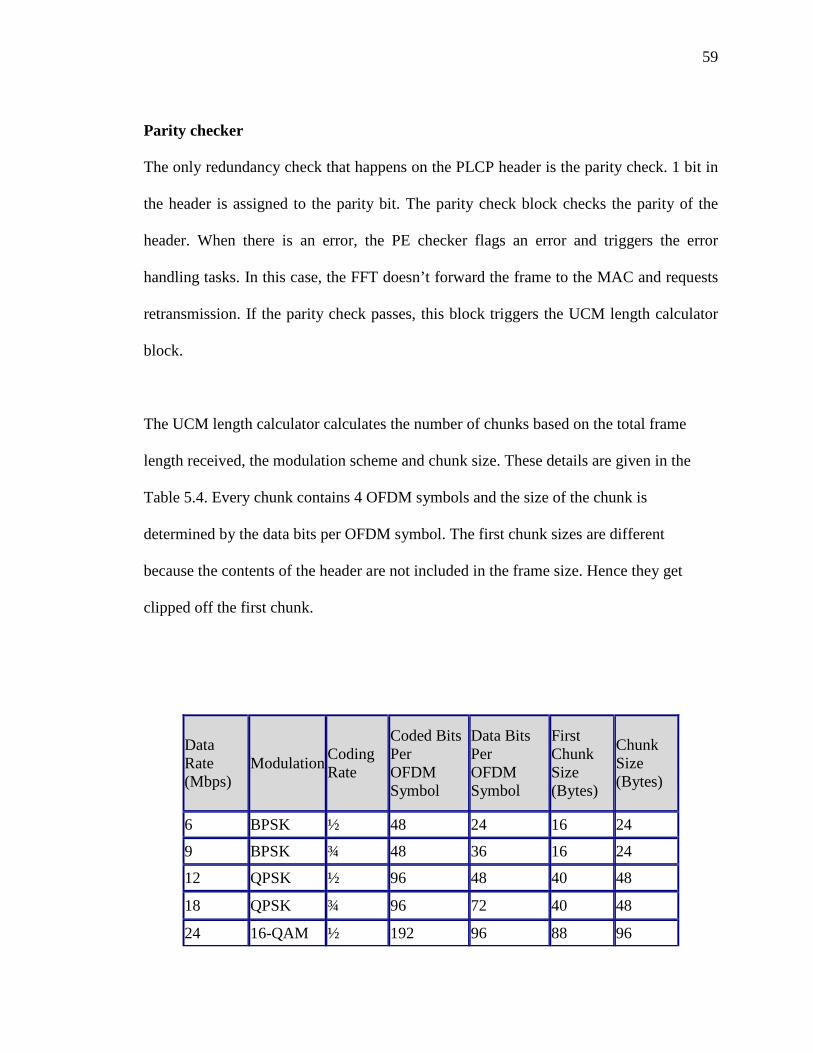
59
Parity checker
The only redundancy check that happens on the PLCP header is the parity check. 1 bit in
the header is assigned to the parity bit. The parity check block checks the parity of the
header. When there is an error, the PE checker flags an error and triggers the error
handling tasks. In this case, the FFT doesn’t forward the frame to the MAC and requests
retransmission. If the parity check passes, this block triggers the UCM length calculator
block.
The UCM length calculator calculates the number of chunks based on the total frame
length received, the modulation scheme and chunk size. These details are given in the
Table 5.4. Every chunk contains 4 OFDM symbols and the size of the chunk is
determined by the data bits per OFDM symbol. The first chunk sizes are different
because the contents of the header are not included in the frame size. Hence they get
clipped off the first chunk.
Data Rate (Mbps)
ModulationCoding Rate
Coded Bits Per OFDM Symbol
Data Bits Per OFDM Symbol
First Chunk Size (Bytes)
Chunk Size (Bytes)
6 BPSK ½ 48 24 16 24
9 BPSK ¾ 48 36 16 24
12 QPSK ½ 96 48 40 48
18 QPSK ¾ 96 72 40 48
24 16-QAM ½ 192 96 88 96

60
Table 5.4: Chunk Sizes for WiFi
Frame Length Forward Block
The frame length block uses the length field in the header to calculate the number of
OFDM symbols based on the following table. The Xilinx generated divider is used.
This block writes the number of symbols in the context field of the outbuffer. This value
is read by the FFT. The UCM in the FFT is responsible for chunking, it uses this value to
determine the number of chunks for the entire frame to fit the required number of OFDM
symbols. The number of OFDM symbols per chunk is set by the user through the register
maps
CRC Check
After the PLCP header handling, the top module sends a header check done to the FFT.
After this, the FFT starts sending the frame to the demodulator which is then passed to
the CRC check block in the checker.
The Frame Check Sequence (FCS) unit calculates CRC over all the data. It processes
36 16-QAM ¾ 192 144 88 96
48 64-QAM 2/3 288 192 136 144
54 64-QAM ¾ 288 216 136 144

61
each byte of the data per cycle and generates a 32-bit CRC. The CRC generator
polynomial is specified in the standard –
G(x) = x32 + x26 + x23 + x22 + x16 + x12 + x11 + x10 + x8 + x7 + x5 + x4 + x2 + x + 1
The CRC generated from a chunk is stored in the context field, which is region 15 of the
output buffer. The initial seed of the CRC block is all 1s. Since the frame arrives in
chunks, the seed for every chunk is the CRC generated by the previous one. This way,
every chunk can be independent and the context field can be used to pass the intermediate
CRC. The MAC Rx then checks the CRC content directly to validate the integrity of the
frame.
All the processing engines have to be tested before implementing on the FPGA. The
following section describes the testbench design used for automated PE verification.
5.3: PE Testbench
Every design has to be backed with extensive testing. In FPGA, the top level entity is
called testbench. The testbench consists of two major components – The device under test
is the user logic and the testbench components.
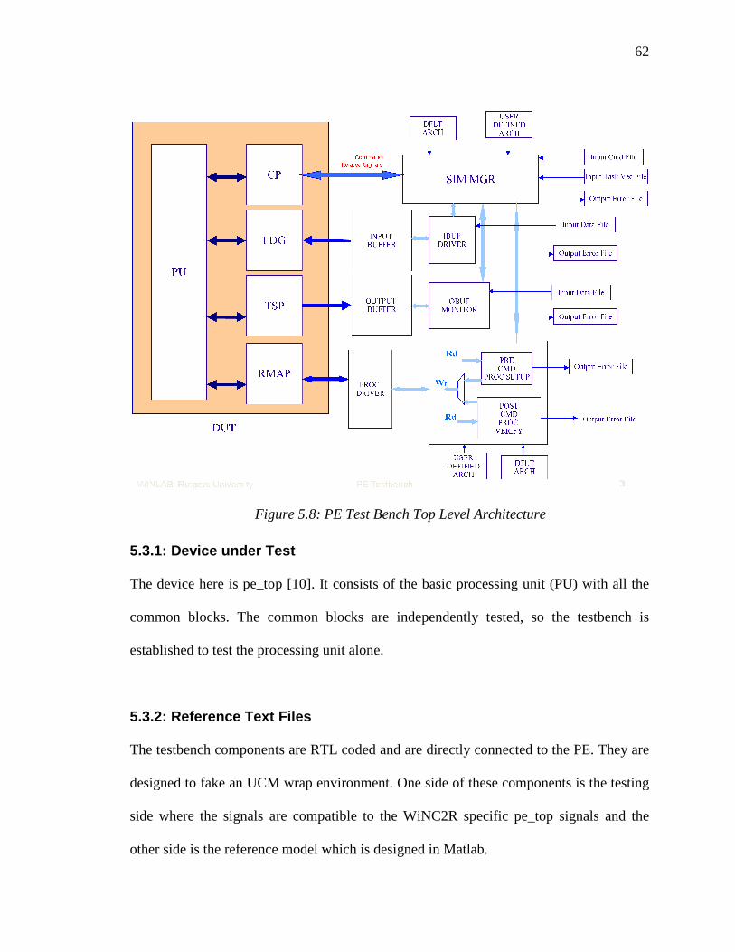
5.3.1: Device under Test
The device here is pe_top
common blocks. The common blocks are independently tested, so the testbench is
established to test the processing unit alone.
5.3.2: Reference Text Files
The testbench components are RTL coded and are directly connected to the PE. They are
designed to fake an UCM wrap environment. One side of these components is the testing
side where the signals are compatible to the WiNC2R specific pe_top signals and the
other side is the reference model which is designed in Matlab.
Figure
5.3.1: Device under Test
is pe_top [10]. It consists of the basic processing unit (PU) with all the
common blocks. The common blocks are independently tested, so the testbench is
established to test the processing unit alone.
Reference Text Files
The testbench components are RTL coded and are directly connected to the PE. They are
designed to fake an UCM wrap environment. One side of these components is the testing
side where the signals are compatible to the WiNC2R specific pe_top signals and the
other side is the reference model which is designed in Matlab.
Figure 5.8: PE Test Bench Top Level Architecture
62
. It consists of the basic processing unit (PU) with all the
common blocks. The common blocks are independently tested, so the testbench is
The testbench components are RTL coded and are directly connected to the PE. They are
designed to fake an UCM wrap environment. One side of these components is the testing
side where the signals are compatible to the WiNC2R specific pe_top signals and the

63
The entire OFDM chain is redesigned in Matlab which acts as the reference for testing.
The model generates input and output buffer data for all processing engines for various
parameters. The parameters include number of frames, frame length, modulation etc.
Following is the list of the text files that are generated for a 14 byte frame with
modulation scheme of BPSK.
1. cmd – This file contains the list of commands for a single testbench session. The
commands are compatible to the tasks mentioned in Chapter 2.
2. Ibuf – This text file is synchronous to the cmd file. It contains the content that is
supposed to be in the input buffer for the corresponding command. The size of the
data is also mentioned in this file

64
3. Obuf – This file contains the correct output buffer contents corresponding to the ibuf f

65
4. Tvec – This file is used to compare the next task vectors coming from the processing
engine to the reference matlab model.
5. Rmap_drv – The register map control words can be manually entered to this text file
with corresponding addresses
6. Rmap_stat – The status messages from the processing engine is written into this file
along with the address.
7. Error files – If the PE produces errors, the output buffer contents that are in error are
written into this file.

66
5.3.3: Testbench Components
1. Ibuf Driver – When triggered, this module writes the content of the ibuf text file to
the inout buffer. It follows the input buffer partitions and writes to the RAM on every
command.
2. Obuf Monitor – This component is responsible for the comparison of the output
buffer to the reference obuf text file. It also generates the error file which shows the
addresses where the word was written in error.
3. Rmap Driver – The RMAP driver has the slave interfaces that are connected to the
RMAP interfaces. This acts like the bus and writes the rmap_drv test file’s content to
the RMAP RAM. The pre-command processor loads the control words to the register
and the post-command processor compares the content of the status register to the
rmap_stat text file.
4. Simulation Manager – This is the main controller of the test bench. It is a light
version of UCM where only the command processes and the next task processes are
simulated. The simulation manager forwards the command from the text file to the

67
command decoder of the processing engine and waits on the command done from the
PE. It also triggers the driver and monitor and keeps the test bench synchronous to the
processing command.

68
Chapter 6:
PE Register Maps and Software
6.1: Register Map
To avoid complexity in hardware, the adaptability and flexibility of the modulator is
implemented in the software. Xilinx provides a software development tool in C that has
functions required to access the FPGA via Joint Test Action Group (JTAG) cable. Hence,
it becomes convenient to code the mapping table in C than VHDL. The software
basically consists of data processing, threshold calculations and writing them to the
designated RAMS. The control and status registers are designated to a block ram
instantiated in RMAP module.
The software – RMAP interface is shown in the figure below.
P
L
B
pe_mod_wrap
Status Register
pe_mod_rmap
Control Register
BPSK
QPSK
16QAM
64QAM
Mapping Table
Bus2IP_RNW
Bus2IP_Addr[15:0]
Bus2IP_Data[31:0]
Bus2IP_WrReqo_rd_en
addr[6:0]
data[32:1]
status control
IP2Bus_Data[31:0]
Xilinx C Functions
xil_read(address);
xil_write(address,data);
fillModTable();
Figure 6.1: PE Mod Register Maps

69
The modulator register map is the crux of the processing engine. It is the only interface
that talks to the user. This part of the processing engine has signals that connect to the
bus. Hence the software can directly read or write into the RAM present in the RMAP.
The control registers are those words that can be written by the user. The control register
in the modulator and demodulator for this release is based on the constellation specified
by the 802.11 standard. The constellation diagram is shown below [15]

70
Figure 6.2: 802.11a constellation diagram
The entire constellation points are converted into complex numbers and arranged in the
from specified in section 5.1.2: . Similarly the demodulation registers are simultaneously
calculated and filled up. The standard specifies a normalization factor to all the
modulations that normalize all the energies. The table is given below
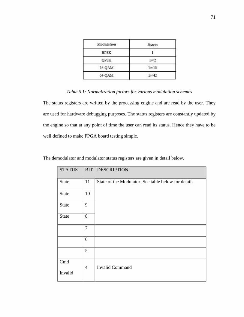
71
Table 6.1: Normalization factors for various modulation schemes
The status registers are written by the processing engine and are read by the user. They
are used for hardware debugging purposes. The status registers are constantly updated by
the engine so that at any point of time the user can read its status. Hence they have to be
well defined to make FPGA board testing simple.
The demodulator and modulator status registers are given in detail below.
STATUS BIT DESCRIPTION
State 11 State of the Modulator. See table below for details
State 10
State 9
State 8
7
6
5
Cmd
Invalid 4 Invalid Command

72
Eof error 3 If eof arrives before sof
Sof error 2 In case of multiple instances of sof frame
Error Flag 1 Error Flag
Task Done 0 Indicates whether the Task was completed
Successfully
MSR(11 to 8) State Description
0000 IDLE Initial State of the Modulator
0001 ST_PTR_ACK Waiting for pointer ack from FDG
0010 ST_SOF Wait for SOF from input buffer
0011 ST_BUF_ACK Waiting for buffer ack from TSP
0100 ST_CTRL_PARA Acquiring control parameters
0101 ST_MOD Modulation State (main)
0110 ST_END_WORD Wait for End of frame
0111 ST_16QAM Waiting for Buffer data for 64QAM
1000 ST_DATA _AVAIL Wait for Data Avail for 64QAM
1001 ST_DATA_EN Data Enable to TSP
1111 ST_DONE Modulation Done
Table 6.2: Modulator Status Register
The PE Demodulator and Checker share a common status register.
State Bit Description
Header Cnt 31-28 Number of Headers received

73
Chunk Cnt 27-24 Number of Chunks received
Flag 19 Always 1
First Chunk 18 Received First Chunk
Last Chunk 17 Received Last Chunk
Err 16 Dmod Error Flag
State 15 Checker Frame State
State 14
State 13
State 12 Checker Length State
State 11
Parity Fail 10 ‘1’ when Header parity fails
Length 0 9 ‘1’ if length from PLCP Header is zero
State 8 Checker States
State 7
State 6 Checker Control States
State 5
State 4 Demodulator States
State 3
State 2
State 1
EOF Err 0 No EOF Found
Table 6.3: Demodulator Checker Status Register
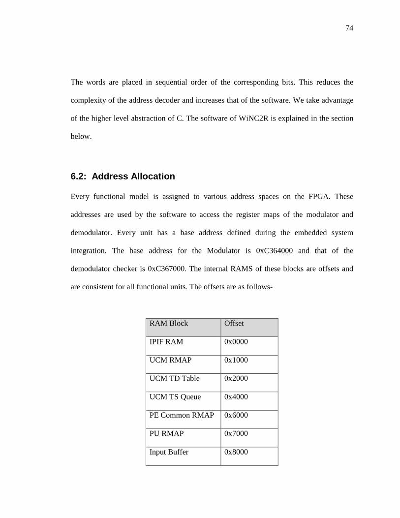
74
The words are placed in sequential order of the corresponding bits. This reduces the
complexity of the address decoder and increases that of the software. We take advantage
of the higher level abstraction of C. The software of WiNC2R is explained in the section
below.
6.2: Address Allocation
Every functional model is assigned to various address spaces on the FPGA. These
addresses are used by the software to access the register maps of the modulator and
demodulator. Every unit has a base address defined during the embedded system
integration. The base address for the Modulator is 0xC364000 and that of the
demodulator checker is 0xC367000. The internal RAMS of these blocks are offsets and
are consistent for all functional units. The offsets are as follows-
RAM Block Offset
IPIF RAM 0x0000
UCM RMAP 0x1000
UCM TD Table 0x2000
UCM TS Queue 0x4000
PE Common RMAP 0x6000
PU RMAP 0x7000
Input Buffer 0x8000

75
Output Buffer 0xC000
Table 6.4: PE RAMs Address Offsets
6.3: Software on WiNC2R
Xilinx provides a software development kit for interfacing the software GUI to the FPGA
board. This kit compiles and builds an image of the software that is loaded on to the
block RAM on the board. It is a Java based application development tool which has
C/C++ editors and the required Xilinx libraries.
The software image which has an extension ‘.elf’ is loaded on to the FPGA via the JTAG
cable. The command interface is provided by the XMD Debugger. XMD stands for
Xilinx Microprocessor Debugger and it communicates with the hardware. Memory read
and write can be performed using this tool. The DAC and ADC interfaces can be tested
using this tool before invoking the software.
The WiNC2R software is written in C. Following will illustrate the functions and
methods used to configure the system.
1. struct complex mod,dmod
The modulation functions generate constellation points that are complex numbers.
2. struct complex modulate(int n,int input,int std_id)
This is the function that returns the complex number representing the constellation
point for input. The argument n is the number of bits associated with input. Since two

76
different sets of modulation schemes are allowed at a time by a single software
session, std_id is used to configure both. In this case std_id = 0 indicates WiFi and
std_id = 1 is WiMax.
This function also calculates the decision regions for the demodulator and stores them
in an array. These values are then forwarded to the RMAP procedure for
demodulator. The values are stored in complex format and then converted to the
WiNC2R compatible data type.
3. struct complex* mod_rmap()
This function generates an array of complex numbers that has to be written to the
modulator register map. As per Table 5.2 the various modulation techniques are
placed in a manner which is interpreted by the modulator’s address decoder. The
array that is returned by this function follows the same convention.
4. Xuint32* mod2xuint(struct complex* mod_val)
Since all these values are fed into the BRAM of the system, they have to be converted
to 32 bit hexadecimal format. Xilinx software development kit provides data types
that are recognizable by the loader. This format is Xuint32 for 32 bit words which are
essentially hexadecimal numbers. The mod2xuint function takes complex numbers as
input and converts them to the xuint32 format.
5. RMAP.c

77
This file consists of all the methods to populate the register maps, RAMS and
initialize queues. It first recognizes the FPGA load, whether it is transmitter or
receiver and then instigates the necessary functions. For modulator and demodulator,
the arrays setup by the above functions are loaded onto the corresponding addresses.
The software initializes the frame and triggers the MAC Tx. The receiver software then
waits for the MAC Rx interrupt flag to be set. Here, the data is verified for its integrity.
The software can be setup by the user dynamically. The cognitive algorithms can be
implemented at the user level in higher level languages. The PE also exhibit chunks
independency i.e. they treat every chunk independent of the other. This means that
multiple frames can be interleaved and sent. This property is helpful for MIMO
applications. The software can be used for multiple frame organization and data flow
allocation.

78
Chapter 7:
Resource Utilization and Timing
7.1: FPGA Resource Utilization
The programmable elements inside a FPGA called Configurable Logic Blocks (CLB). A
FPGA consists of slices which consist of configurable switch matrix with 4 or 6 inputs,
known as look-up tables or function generators (FG), some multiplexers and flip-flops
(FF). A configurable logic block consists of 4 such slices. This combined architecture
gives benefits in the final system such as increased performance of logic execution.
FPGAs are also equipped with Block RAMs which allows on-chip memory allocations.
These memories are used for input/output buffers, TD tables and register maps. The
DSP48E is a Virtex5 FPGA slice that are used for powerful DSP applications and math
intensive processing that eliminate the use of general purpose routing and other logic
resources.
The synthesis tool in FPGA design converts the VHDL code to these basic logic blocks.
The design is assigned specific locations on the FPGA. Hence, every design is restricted
by these FPGA resources. The area utilization is helpful to determine the robustness and
scalability of the design.
The following section provides the utilization in terms of percentage occupied on Xilinx
Virtex5 FPGA.
7.1.1: Transmitter Utilization

79
FG Slices FF BRAM DSP48Es Top Level 0.51% 0.90% 0.88% 0.00% 0.47% Processor 9.13% 9.91% 9.70% 16.80% 0.47% PE pe_pcie 0.72% 0.99% 0.97% 0.00% 0.00% pe_mac_tx 1.55% 1.56% 1.19% 0.00% 0.00% pe_hdr 0.98% 1.05% 1.03% 0.00% 0.16% pe_mod 0.67% 0.69% 0.67% 0.00% 2.05% pe_tx_fft 7.20% 7.32% 7.16% 3.28% 11.25% Total 11.12% 11.62% 11.02% 3.28% 13.46% FU fu_pcie 0.77% 0.77% 0.54% 0.00% 0.00% fu_mac_tx 3.76% 3.76% 2.74% 0.41% 0.47% fu_hdr 3.22% 3.22% 2.61% 0.00% 0.63% fu_mod 2.97% 2.98% 2.19% 0.41% 0.78% fu_tx_fft 2.39% 2.40% 1.72% 0.00% 0.31% Total 13.11% 13.13% 9.80% 0.82% 2.19% UCM Wrap fu_ucm_wrap 10.30% 10.31% 7.36% 0.00% 2.81% fu_ucm_wrap x 4 41.20% 41.22% 29.43% 0.00% 6.56% Total 41.20% 41.22% 29.43% 0.00% 6.56%
Total Resource 75.08% 76.78% 60.83% 20.90% 21.88%
Table 7.1: Transmitter Utilization
7.1.2: Receiver Utilization
FG Slices FF BRAM DSP48Es
Top level 1.00% 1.24% 1.21% 0.00% 0.78%
Processor 9.13% 9.91% 9.70% 16.80% 0.47%
PE
pe_pcie 0.72% 0.99% 0.97% 0.00% 0.00%
pe_mac_rx 1.23% 1.24% 0.94% 0.00% 0.16%
pe_dmod 2.09% 2.09% 1.81% 0.00% 0.47%
pe_sync 33.40% 33.40% 31.00% 9.84% 34.53%
Total 37.44% 37.72% 34.71% 9.84% 35.16%
FU
fu_pcie 0.77% 0.77% 0.54% 0.00% 0.00%
fu_mac_rx 2.26% 2.27% 1.64% 0.00% 0.47%
fu_dmod 2.26% 2.26% 1.64% 0.00% 0.47%
fu_sync 2.27% 2.28% 1.65% 0.00% 0.47%

80
Total 7.57% 7.58% 5.47% 0.00% 1.41%
fu_ucm_wrap 10.30% 10.31% 7.36% 0.00% 2.81%
fu_ucm_wrap x 3 30.90% 30.92% 22.07% 0.00% 6.56%
Total 30.90% 30.92% 22.07% 0.00% 6.56%
Total Resource 86.04% 87.36% 73.15% 26.64% 44.38% Table 7.2: Receiver Utilization
From the above tables, we observe that almost 80-85% of the FPGA has been utilized for
the design. Fitting more design into this will complicate the routing process and increase
the time for programming FPGA. Hence, for the future designs, we have eliminated the
PCIe block and combined the synchronizer and demodulator.
The modulator and demodulator utilization is highlighted in the table above. It has also
been noted that most of the space is occupied by multiple UCM. Each processing engine
requires UCM which means that addition of any functional unit would cost 10% area.
7.2: Timing Analysis
In this section, we calculate the Modulator and Demodulator processing latency. Table
7.3 illustrates the number of clock cycles required by the modulator to process various
frame sizes from 500 to 1500 bytes. The mid-chunk latency includes the time required by
the UCM to process the chunk and trigger modulation task for the next chunk.
Modulation Frame Size (bytes)
500 750 1000 1250 1500 Mid Chunk
Latency BPSK 53724 91107 105375 133236 159147 1918 QPSK 25890 38868 53725 66696 79676 1890 16QAM 12936 20448 25947 33438 38939 1678 64QAM 8113 13035 17904 21192 26061 1730
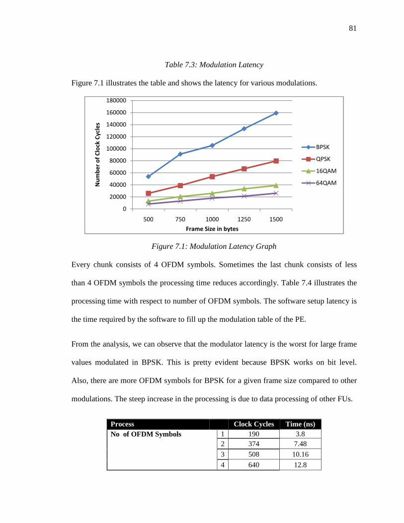
81
Table 7.3: Modulation Latency
Figure 7.1 illustrates the table and shows the latency for various modulations.
Figure 7.1: Modulation Latency Graph
Every chunk consists of 4 OFDM symbols. Sometimes the last chunk consists of less
than 4 OFDM symbols the processing time reduces accordingly. Table 7.4 illustrates the
processing time with respect to number of OFDM symbols. The software setup latency is
the time required by the software to fill up the modulation table of the PE.
From the analysis, we can observe that the modulator latency is the worst for large frame
values modulated in BPSK. This is pretty evident because BPSK works on bit level.
Also, there are more OFDM symbols for BPSK for a given frame size compared to other
modulations. The steep increase in the processing is due to data processing of other FUs.
Process Clock Cycles Time (ns) No of OFDM Symbols 1 190 3.8
2 374 7.48
3 508 10.16
4 640 12.8
0
20000
40000
60000
80000
100000
120000
140000
160000
180000
500 750 1000 1250 1500
Nu
mb
er
of
Clo
ck C
ycl
es
Frame Size in bytes
BPSK
QPSK
16QAM
64QAM
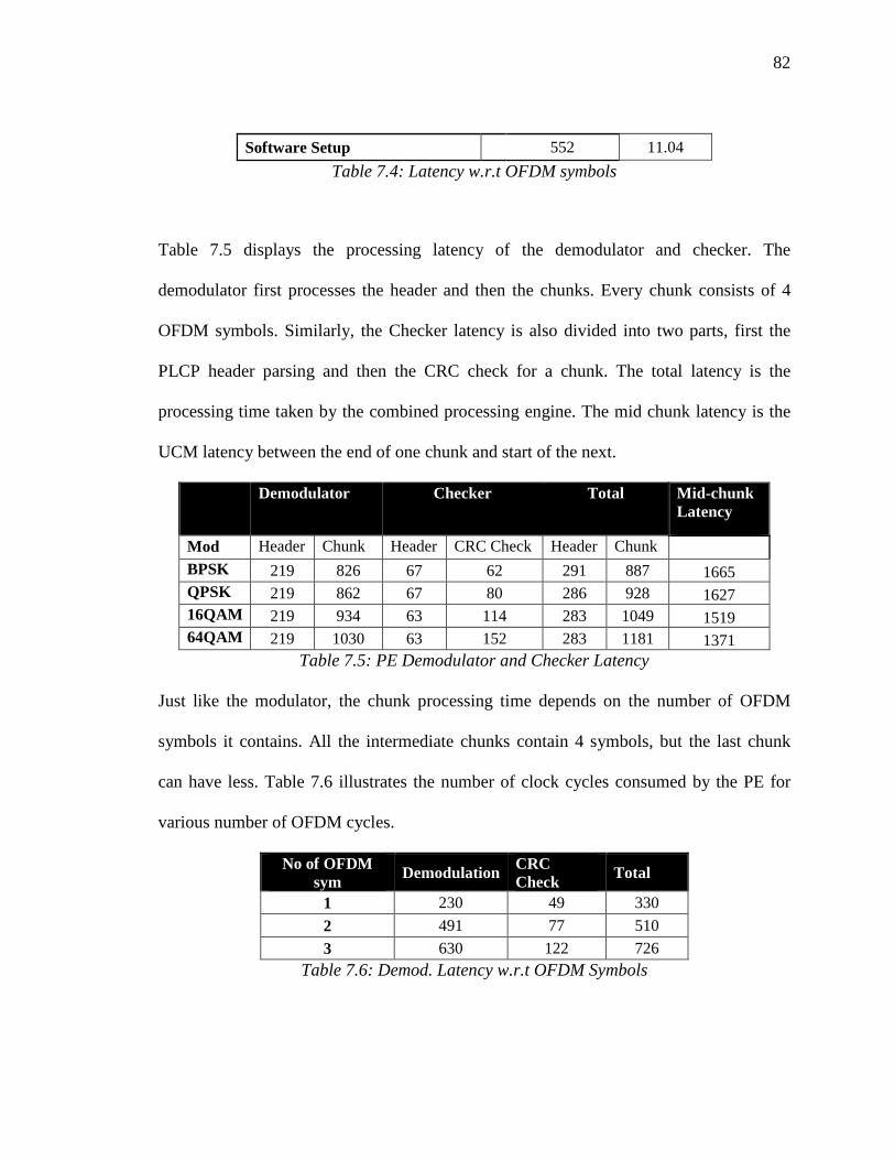
82
Software Setup 552 11.04
Table 7.4: Latency w.r.t OFDM symbols
Table 7.5 displays the processing latency of the demodulator and checker. The
demodulator first processes the header and then the chunks. Every chunk consists of 4
OFDM symbols. Similarly, the Checker latency is also divided into two parts, first the
PLCP header parsing and then the CRC check for a chunk. The total latency is the
processing time taken by the combined processing engine. The mid chunk latency is the
UCM latency between the end of one chunk and start of the next.
Demodulator Checker Total Mid-chunk Latency
Mod Header Chunk Header CRC Check Header Chunk
BPSK 219 826 67 62 291 887 1665 QPSK 219 862 67 80 286 928 1627 16QAM 219 934 63 114 283 1049 1519 64QAM 219 1030 63 152 283 1181 1371
Table 7.5: PE Demodulator and Checker Latency
Just like the modulator, the chunk processing time depends on the number of OFDM
symbols it contains. All the intermediate chunks contain 4 symbols, but the last chunk
can have less. Table 7.6 illustrates the number of clock cycles consumed by the PE for
various number of OFDM cycles.
No of OFDM sym Demodulation CRC
Check Total
1 230 49 330
2 491 77 510
3 630 122 726 Table 7.6: Demod. Latency w.r.t OFDM Symbols
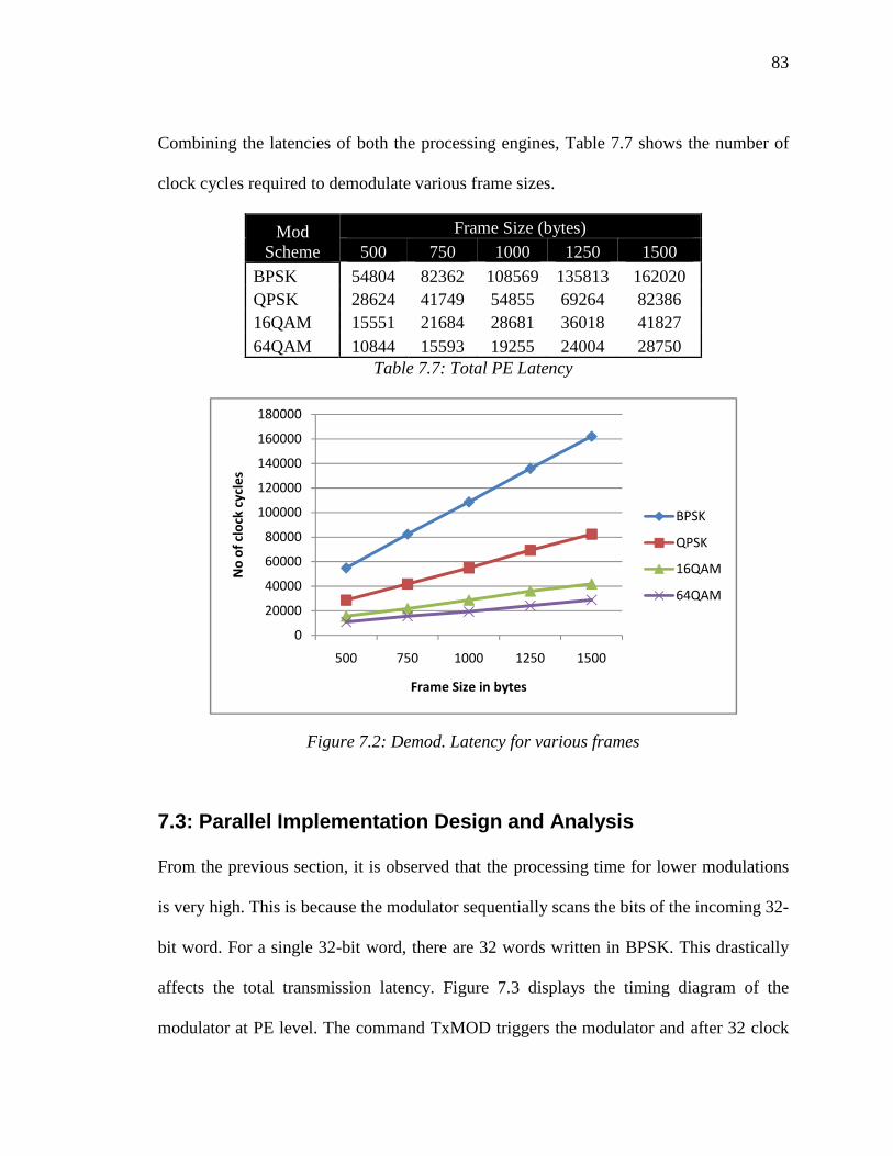
83
Combining the latencies of both the processing engines, Table 7.7 shows the number of
clock cycles required to demodulate various frame sizes.
Mod Scheme
Frame Size (bytes) 500 750 1000 1250 1500
BPSK 54804 82362 108569 135813 162020 QPSK 28624 41749 54855 69264 82386 16QAM 15551 21684 28681 36018 41827 64QAM 10844 15593 19255 24004 28750
Table 7.7: Total PE Latency
Figure 7.2: Demod. Latency for various frames
7.3: Parallel Implementation Design and Analysis
From the previous section, it is observed that the processing time for lower modulations
is very high. This is because the modulator sequentially scans the bits of the incoming 32-
bit word. For a single 32-bit word, there are 32 words written in BPSK. This drastically
affects the total transmission latency. Figure 7.3 displays the timing diagram of the
modulator at PE level. The command TxMOD triggers the modulator and after 32 clock
0
20000
40000
60000
80000
100000
120000
140000
160000
180000
500 750 1000 1250 1500
No
of
clo
ck c
ycl
es
Frame Size in bytes
BPSK
QPSK
16QAM
64QAM

84
cycles the first data is written to the output buffer. A single word is written in 1 clock
cycle (marked in yellow) and the dead time between two data-writes is 2 clock cycles
(marked in grey).
ACTION Signal
TxMOD
Input Buffer Requests
Output Buffer Requests
Data Write
1 clock cycle
Dead Time
2 clock cycles
Parameter Fetch Input Data Fetch Setup Output Buffer Modulate
10 Clock Cycles 9 Clock Cycles 11 Clock Cycles
Figure 7.3: Modulator Timing Diagram
The overall latency of processing can be reduced by eliminating this dead time. Since it
takes 3 clock cycles to process the input bits, we can implement three modulators in
parallel. In this way, each of them gets one slot (clock cycle) to write an output word.
Figure 7.4 shows the architectural diagram of a parallel modulator implementation in a
single PE.

85
pe_mod
Input Word
31 0
...
...
OUTPUT
ARBITER
pe_mod 1
table
pe_mod 2
table
pe_mod n
table
INPUT
SWITCH
Output Buffer
CONTROL BLOCK
Figure 7.4: Parallel Modulator Implementation
The input switch constantly feeds the modulators with bits. The output arbiter is
responsible for collecting the date from the modulators and writing them sequentially to
the output buffer. The reduction in latency is shown in the table below.
Mod Size of Frame
500 750 1000 1250 1500 Avg
BPSK 69.54 69.65 69.71 69.75 69.78 69.69
QPSK 70.28 70.51 70.64 70.71 70.75 70.58
16QAM 71.74 72.14 72.29 72.43 72.50 72.22
64QAM 61.70 62.32 55.69 67.36 73.30 64.07
Percentage Reduction
Table 7.8: Latency Reduction in Modulator
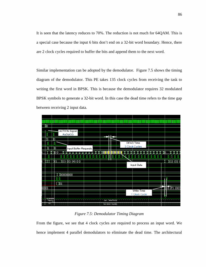
86
It is seen that the latency reduces to 70%. The reduction is not much for 64QAM. This is
a special case because the input 6 bits don’t end on a 32-bit word boundary. Hence, there
are 2 clock cycles required to buffer the bits and append them to the next word.
Similar implementation can be adopted by the demodulator. Figure 7.5 shows the timing
diagram of the demodulator. This PE takes 135 clock cycles from receiving the task to
writing the first word in BPSK. This is because the demodulator requires 32 modulated
BPSK symbols to generate a 32-bit word. In this case the dead time refers to the time gap
between receiving 2 input data.
Figure 7.5: Demodulator Timing Diagram
From the figure, we see that 4 clock cycles are required to process an input word. We
hence implement 4 parallel demodulators to eliminate the dead time. The architectural
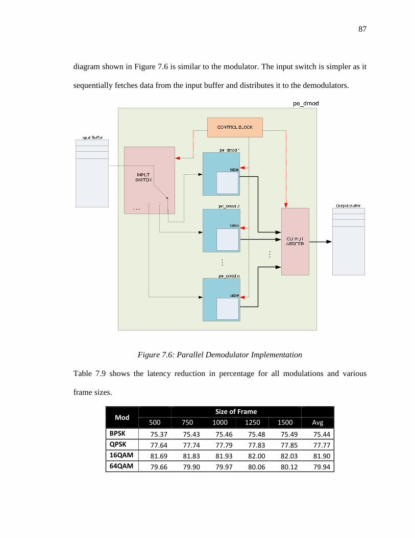
87
diagram shown in Figure 7.6 is similar to the modulator. The input switch is simpler as it
sequentially fetches data from the input buffer and distributes it to the demodulators.
Figure 7.6: Parallel Demodulator Implementation
Table 7.9 shows the latency reduction in percentage for all modulations and various
frame sizes.
Mod Size of Frame
500 750 1000 1250 1500 Avg
BPSK 75.37 75.43 75.46 75.48 75.49 75.44
QPSK 77.64 77.74 77.79 77.83 77.85 77.77
16QAM 81.69 81.83 81.93 82.00 82.03 81.90
64QAM 79.66 79.90 79.97 80.06 80.12 79.94

88
Percentage Reduction
Table 7.9: Latency Reduction in Demodulator
The table shows that there is a drastic decrease in the processing timing because of the
additional four demodulators used. The number of clock cycles reduces to almost 1/4th of
the original.
Since we are adding more blocks to implement parallel engines, a single PE now will
occupy more space on the FPGA. The tables below show the area utilization of this
implementation.
Area on FPGA (%)
Control Input Switch
Output Switch Mod 3
Mods PE_MOD % Increase
Function Generators 0.07 0.17 0.19 0.58 1.89 0.67 64.55 CLB Slices 0.31 0.35 0.19 0.58 1.35 0.69 48.89 Dffs or Latches 0.3 0.34 0.12 0.46 0.94 0.67 28.72 Block RAMs 0 0 0 0.82 2.46 0.82 66.67 DSP48Es 0 0 0 0.78 2.34 0.78 66.67
Table 7.10: Parallel Modulator Area Utilization
Area on FPGA (%)
Control Input
Switch Output Switch Demod 4
Demods PE_DMOD % Increase
Function Generators 0.07 0.17 0.19 4.02 12.21 4.02 75.12
CLB Slices 0.31 0.35 0.19 4.02 11.67 4.02 73.86
Dffs or Latches 0.3 0.34 0.12 0.86 2.14 0.86 68.15
Block RAMs 0 0 0 1.64 4.92 1.64 75.00
DSP48Es 0 0 0 4.38 13.14 4.38 75.00
Table 7.11: Parallel Demodulator Area Utilization
We use 3 modulating engines in parallel; as a result the total area utilization has increased
three times. Similarly, the demodulator area has increased four times.

89
We can choose the parallel implementation based on the application. In WiNC2R’s
802.11a-Lite implementation, the main focus was reduction of area. The UCM wrap
takes up most of the resources. It was necessary that we reduce the area used by the
processing engines. Thus, only one modulator and demodulator was used. If the
application is restricted to latency, then we can use the parallel implementation with the
cost of FPGA resource. The timing and area analysis can be used to make decisions
regarding the choice of implementation.
90
Chapter 8: Conclusion
The thesis discussed the design on the modulator and demodulator on the WiNC2R. We
explored the flexibility of these engines with respect to the modulation schemes. The
constellation points can be programmed by the user dynamically. These blocks are a part
of the 802.11a-lite implementation of the Virtual Flow Pipeline and have shown
successful results in simulation and hardware.
We have observed that the involvement of software drastically reduces the processing
time. Hence the data signal processing is left to Virtex5 FPGA. The task and data flow is
setup by software. The concept of having a dynamic data flow for every session and
every frame is called virtual flow pipelining.
We have discussed the WiNC2R platform that implements the virtual flow pipelining for
802.11a-lite protocol. The transmitter and receiver flow was divided into various global
tasks. The task flow demonstrated in the first release is as follows –
• Transmitter: MAC – HEADER – MODULATOR – IFFT
• Receiver: SYNCHRONIZER – FFT – DEMODULATOR – CHECKER – MAC
It has been shown that the WiNC2R is able to send successful frames across the entire
chain with the above flow. The FU chain is setup in the global task table and any FU can
be added between frames. Protocol inter-operability is achieved this way by plugging the
required FU inside the flow. Hence, the more Functional Units are designed for better
performance, scalability and robustness.

91
We have also created the functional unit flexible within the restrictions of hardware. With
the help of mapping table inside the modulator and the decision table inside the
demodulator, the user has more freedom to tune these functional units. Such units find
many applications especially in vehicular environments where the channel must be
constantly monitored and the radio parameters must change on the fly. Research institutes
can also use the functional units for experimenting with new protocols and study its
performance on various environments.
The timing and area analysis can be used for future releases to calculate latency and
utilization. The values are constant for every chunk and can be used as estimates for
calculating system latency. From the timing analysis, it is observed that UCM needs to be
further improved in terms of latency. There will be a great loss in data rate for huge frame
sizes due to the mid-chunk latency. In terms of area, the modulator and demodulator take
up an insignificant amount of resources. But again, due to UCM complexity, every
instance adds 10% to the total area. Hence, more research has to be dedicated to UCM to
reduce area or reuse logic.
We have also proposed a parallel modulator/demodulator implementation that reduces the
latency by 1/3rd. The cost of reducing this latency is FPGA area which increases almost 3
times. This analysis can be used in the future releases to make decisions on implementing
the modulator and demodulator.

92
Future Work
1) The modulator design can be improved for complicated constellation points. This
type of RAM structure supports only rectangular constellations. The designed can
be improved further for phase shift modulation schemes.
2) Error coder and decoder can also be designed in the similar fashion where the
mapping table can contain the codeword dictionary. Encryption of data is also
possible where the user can use the software to implement various techniques and
the processing engine picks up the coded message from the register map.
3) We can save more FPGA resource area by reusing the modulator code. Since both
the processing engines operate using look-up tables, the same processing engine
can be reused for encoding or encryption.
4) The area of the entire system can also be reduced by clustering multiple
Functional Units to a single unit control module. This also gives more room to
accommodate more processing engines.
5) The software of WiNC2R needs to be improved with regards to the traffic
generation, dynamic flow setups and user-friendliness.

93
References
[1] Z. Miljanic, I. Seskar, K. Le, and D. Raychaudhuri, WINLAB Network Centric Cognitive Radio Hardware Platform - WiNC2R, in Proceedings of International Conference on Cognitive Radio Oriented Wireless Networks and Communications, Orlando, Florida, 2007. CrowCom 2007.
[2] Zoran Miljanic and Predrag Spasojevic, Resource Virtualization with Programmable Radio Processing Platform WICON 2008, Maui Hawaii, USA.
[3] Network Centric Cognitive Radio (WiNC2R) http://www.winlab.rutgers.edu/docs/focus/WiNC2R.html
[4] GNURadio wiki page : http://gnuradio.org/trac [5] WARP wiki page : http://warp.rice.edu/trac [6] Xilinx Documentation : http://www.xilinx.com/support/documentation/ [7] Innovative Integration’s X5-400M Manual : http://www.innovative-
dsp.com/support/manuals/X5-400M.pdf [8] Innovative Integration’s X5-400M Logic User Guide [9] WiNC2R wiki page [10] WiNC2R – Processing Engine Documents [11] WiNC2R – Functional Unit Documents [12] WiNC2R – Network Centric Protocol Documents. [13] S.Jain. Hardware and software for WiNC2R. Masters Thesis, Rutgers
University, October 2008. [14] Vijayant Bhatnagar. Performance and Hardware Complexity Analysis of
Programmable Radio Platform for MIMO OFDM Based WLAN Systems. Masters Thesis, Rutgers University, May 2008.
[15] “IEEE 802.11a Physical and MAC Layer Specifications,” IEEE 802.11a, 1999. [16] S.Satarkar. Performance Analysis of WiNC2R Platform.
Masters Thesis, Rutgers University, August 2009

94
Abbreviations
ADC Analog to Digital Converters
BPSK Binary Phase Shift Keying
BRAM Block Random Access Memory
CLB Configurable Logic Block
CP Command Processor
CRC Cyclic Redundancy Check
DAC Digital to Analog Converters
DDR Double Data Rate
DMA Direct Memory Access
DMOD Demodulator
DP Data Processors
EOF End of Frame
FCS Frame Check Sequence
FDG Frame Delimiter and Generator
FFT Fast Fourier Transform
FIFO First In First Out
FPGA Field Programming Gate Array
FU Functional Unit
GNU GNU Not Unix
GTT Global Task Descriptor
HDL Hardware Description Language

95
HDR Header
IFFT Inverse Fast Fourier Transform
IPIF Intellectual Property Interface
JTAG Joint Test Action Group
MAC Medium Access Control
MDM Microprocessor Debug Module
MIMO Multiple In Multiple Out
MOD Modulator
MPMC Multi Port Memory Controller
MSPS Mega Samples Per Second
NCO Numerically Controlled Oscillator
OFDM Orthogonal Frequency Division Multiplexing
OPB On-Chip Peripheral Bus
PCI Peripheral Component Interconnect
PE Processing Engine
PHY Physical Layer
PLB Processor Logic Bus
PLCP Physical Layer Convergence Protocol
QAM Quadrature Amplitude Modulation
QDR Quad Data Rate
QoS Quality of Service
QPSK Quadrature Phase Shift Keying
96
RF Radio Frequency
RMAP Register Maps
RSSI Received Signal Strength Indicator
RTL Register Transfer Level
Rx Receiver
SDR Software Defined Radios
SISO Single In Single Out
SoC System on Chip
SOF Start of Frame
SWIG Simplified Wrapper and Interface Generator
SYNC Synchronizer
TD Task Descriptor
TSP Task Spawning Processor
Tx Transmitter
UCM Unit Control Module
USB Universal Serial Bus
USRP Universal Software Radio Peripheral
VFP Virtual Flow Paradigm
WARP Wireless Open Access Research Platform
WiFi Wireless Fidility
WiMAX Worldwide Interoperability for Microwave Access
WiNC2R WINLAB Network Centric Cognitive Radio

97
WINLAB Wireless Information Network Laboratory
WLAN Wireless Local Area Network
XMC Express Mezzanine Card