tesi master atroshchenko
TRANSCRIPT

in collaboration with Confindustria Veneto
MASTER THESIS
in
“Surface Treatments for Industrial Applications”
High temperature annealing for thermally
diffused Nb3Sn
Supervisor: Prof. V. Palmieri
Co-Supervisor: Dr. A.A.Rossi
Academic Year 2009-10
Student: Dott. Atroshchenko Konstantin
Matr. N°: 1002712
ISTITUTO NAZIONALE
DI FISICA NUCLEARE
Laboratori Nazionali di Legnaro
UNIVERSITÀ DEGLI
STUDI DI PADOVA
Facoltà di Scienze MM.NN.FF.

Contents 2
Contents 3
Contents
Abstract………................................................................................................................................. 6
Introduction………………………………………………………………………………………… 7
0.1 Particle accelerators…………………………………………………………………………. 7
0.2 Fundamentals of superconductivity………………………………………………………… 7
0.2.1 Meissner effect………………………………………………………………………. 8
0.2.2 London equations and London penetration depth………………………………….. 8
0.2.3 BCS theory………………………………………………………………………….. 9
0.2.4 Superconductor surface resistance…………………………………………………. 10
0.2.5 Residual resistance…………………………………………………………………. 10
0.2.6 Critical magnetic field……………………………………………………………… 11
0.3 Superconductive cavities…………………………………………………………………… 11
0.3.1 Advantages of superconductive cavities…………………………………………… 12
0.3.2 RF – fields in cavities………………………………………………………………. 13
0.3.3 Accelerating fields………………………………………………………………….. 14
0.3.4 Peak surface fields………………………………………………………………….. 14
0.3.5 RF – power dissipation and cavity quality…………………………………………. 15
1. Materials for superconductive cavities………………………………………………………. 17
1.1 Bulk metals………………………………………………………………………………… 19
1.2 B1 materials………………………………………………………………………………… 19
2. A-15 materials…………………………………………………………………………………. 21
2.1 Crystal structure……………………………………………………………………………. 21
2.2 Critical temperature and compositions…………………………………………………….. 22
3. 6 GHz cavities…………………………………………………………………………………. 29
3.1 Application…………………………………………………………………………………. 29
3.2 Geometry…………………………………………………………………………………… 30
3.3 Fabrication technique………………………………………………………………………. 31
4. Nb3Sn…………………………………………………………………………………………... 33
4.1 Chemical and physical properties………………………………………………………….. 33
4.2 Tc as a function of atomic Sn content……………………………………………………… 34
4.3 Nb3Sn phase formation (diffusion fundamentals)…………………………………………. 35
Contents 4
5. Inductive annealing fundamentals…………………………………………………………. 39
5.1 Introduction………………………………………………………………………………. 39
5.2 Magnetic material properties…………………………………………………………….. 39
5.2.1 Different kinds of magnetic materials……………………………………………. 40
5.2.2 Domains………………………………………………………………………...… 41
5.2.3 Hysteresis…………………………………………………………………………. 41
5.2.4 Skin depth………………………………………………………………………… 42
5.3 Practical implementation of induction heating system…………………………………… 43
5.3.1 Parallel resonant tank circuit……………………………………………………… 43
5.3.2 Impedance matching...……………………………………………………………. 44
5.3.3 LCLR work coil…………………………………………………………...……… 46
5.3.4 Conceptual schematic…………………………………………………………….. 47
5.3.5 Fault tolerance…………………………………………………………………….. 48
5.3.6 Power control methods…………………………………………………………… 48
6. Nb3Sn by «double furnace» Liquid Tin Diffusion fabrication technique……………….. 50
6.1 Introduction……………………………………………………………………………….. 50
6.2 Nb3Sn samples production……………………………………………………………...… 50
6.2.1 L – samples……………………………………………………………………….. 50
6.2.2 Preliminary surface treatments (mechanical treatment and BCP)………………... 51
6.2.3 Glow discharge...…………………………………………………………………. 52
6.2.4 Anodization ....……………………………………………………………….…… 54
6.2.5 Chemical etching…………………………………………………………….…… 55
6.2.6 Experimental apparatus for dipping......………………………………………….. 56
6.2.7 Dipping………………...…………………………………………………………. 59
6.2.8 Resistive furnace annealing………………………………………………………. 61
6.2.9 Obtained films and problem of residual Tin droplets……………..……………… 61
6.3 Nb3Sn 6 GHz cavities production...……………………………………………………… 63
6.3.1 Preliminary surface treatments…………………………………………………… 63
6.3.2 Dipping…………………………………………………………………………… 69
6.3.3 Resistive furnace annealing……….……………………………………………… 70
6.3.4 Obtained coatings………………………………………………………………… 71
6.4 Nb3Sn 6 GHz cavities analysis...………………………………………………………… 74
6.4.1 Internal surface pictures by mini-camera....…………………………….………… 74
6.4.2 RF – test…………….…………………………………………………………….. 75
7. Nb3Sn by LTD with high temperature annealing…………………………………………. 77
7.1 Nb3Sn samples production………….…………………………………………………….. 77
7.1.1 L – samples and LL – samples……….…………………………………………… 77
7.1.2 Preliminary surface treatments (mechanical treatment and BCP)………………… 78

Contents 5
7.1.3 Procedure of dipping………………………………………………………………. 78
7.1.4 Inductive annealing experimental apparatus………………………….…………… 79
7.1.5 Inductive annealing procedure…………………………………………………….. 82
7.1.6 Obtained films...…………………………………………………………………… 84
7.2 Nb3Sn samples analysis....………………………………………………………………… 86
7.2.1 XRD...……………………………………………………………………………… 86
7.2.2 Inductive Tc and ΔTc measurement………………………………………………... 87
7.3 Nb3Sn 6 GHz cavities production....……………………………………………………… 88
7.3.1 Preliminary surface treatments.....…………………………………………………. 88
7.3.2 Dipping…………………………………………………………………………….. 89
7.3.3 Inductive annealing………………………………………………………………… 90
7.3.4 Post – annealing treatments.....…………………………………………………….. 97
7.3.5 High pressure rinsing………………………………………………………………. 97
7.4 Nb3Sn 6 GHz cavities analysis……………………………………………………………. 98
7.4.1 RF – test……………………………………………………………………………. 98
8. Discussion….………………………………………………………………………………… 100
9. Conclusions………………………………………………………………………………….. 104

Index 6

Abstract 7
Abstract
International Committee for Future Accelerators recommended that the Linear Collider
design has to be based on the superconducting technology. And this is the reason why the
international scientific society directed efforts to improving superconductive technology and
reducing its cost.
In this work, in the framework of researching a valid alternative to Nb for RF
superconducting cavities, thin film Nb3Sn has been investigated. The goal will be the achievement
of superconducting cavities working better than the Nb ones at 4.2 K.
In order to improve the existing technology of substrates coating by thermally diffused
Nb3Sn a new high temperature annealing technology has been developed. In the first part of the
work, is given the short theoretical review of RF superconductivity, main superconductors that are
used to be a good alternative to a pure Nb and fundamentals of the induction heating theory. Second
part is dedicated to the existing double furnace technology, developed in the superconductivity lab
in LNL. The influence of preliminary surface treatments like glow discharge of the sample,
anodization and chemical etching on the quality of thermally diffused Nb3Sn was studied. And in
the third part is given the description of the new induction heating system, suggested for annealing
of the 6 GHz cavities. Also in the third part we will go through the results of coating samples and
cavities with thermally diffused Nb3Sn with high temperature annealing and the results of the RF –
test.
Finally, it is important to mention, that from the very beginning of investigation the
induction heating for annealing 6 GHz cavities it became clear that the technology has an enormous
potential in producing thermally diffused Nb3Sn.
Introduction 8
Introduction
0.1 Particle accelerators
In the past century, physicists have explored smaller and smaller scales, cataloguing and
understanding the fundamental components of the universe, trying to explain the origin of mass and
probing the theory of extra dimensions. And in recent years, experiments and observations have
pointed to evidence that we can only account for a surprising five percent of the universe.
The International Linear Collider will give physicists a new cosmic doorway to explore energy
regimes beyond the reach of today’s accelerators. The proposed electron-positron collider (ILC) will
complement the Large Hadron Collider, a proton-proton collider at the European Center for Nuclear
Research (CERN) in Geneva, Switzerland, together unlocking some of the deepest mysteries in the
universe. Consisting of two linear accelerators that face each other, the ILC will hurl some 10 billion
electrons and their anti-particles, positrons, toward each other at nearly the speed of light.
Accelerator cavities give the particles more and more energy until they smash in a blazing crossfire
at the center of the machine. Stretching approximately 35 kilometers in length, the beams collide
14,000 times every second at extremely high energies (500 GeV). Each spectacular collision creates
an array of new particles that could answer some of the most fundamental questions of all time. The
current baseline design allows for an upgrade to a 50-kilometers, 1 TeV machine during the second
stage of the project.
Planning, designing, funding and building the proposed International Linear Collider will require
global participation and global organization. An international team of more than 60 scientists and
engineers leads the Global Design Effort (GDE) for the ILC. The GDE team sets the design and
priorities for the work of scientists and engineers around the world. From the senior physicist to the
undergraduate student, about 2000 people from more than 100 universities and laboratories in over
two dozen countries are collaborating to build the ILC, the next-generation particle accelerator.
0.2 Fundamentals of superconductivity
Superconductivity is the ability of certain materials to conduct electric current with practically
zero resistance. This produces interesting and potentially useful effects. For a material to behave as a
superconductor, low temperatures are required. Superconductivity was first observed in 1911 by H.
K. Onnes, a Dutch physicist. His experiment was conducted with elemental mercury at 4K, the
temperature of liquid helium. He observed that the electrical resistance disappeared completely near
the Tc temperature, which is the characteristic of the material.

Fundamentals of superconductivity 9
0.2.1 Meissner effect
The Meissner effect is the expulsion of a magnetic field from a superconductor during its
transition to the superconducting state. Walther Meissner and Robert Ochsenfeld discovered the
phenomenon in 1933 by measuring the magnetic field distribution outside superconducting tin and
lead samples [1]. The samples, in the presence of an applied magnetic field, were cooled below what
is called their superconducting transition temperature. Below the transition temperature the samples
canceled all magnetic fields inside, which means they became perfectly diamagnetic. Perfect
diamagnetism is the phenomenon when not only a magnetic field is excluded from entering a
superconductor, but also that a field in an originally normal sample is expelled as it is cooled
through Tc.
0.2.2 London equations and London penetration depth
The London equations, developed by brothers Fritz and Heinz London in 1935, relate current
to electromagnetic fields in and around a superconductor. Perhaps the simplest meaningful
description of superconducting phenomena, they form the genesis of almost any modern
introductory text on the subject. A major feature of the equations is their ability to explain
the Meissner effect, wherein a material exponentially expels all internal magnetic fields as it crosses
the superconducting threshold.
There are two London equations when expressed in terms of measurable fields:
(0.1)
(0.2)
where
js – the superconducting current;
E and B – electric and magnetic fields within the superconductor;
E – charge of an electron;
M – electron mass;
ns – phenomenological constant loosely associated with a number density of superconducting
carriers.
If equation (0.2) is manipulated by applying Ampere’s law
Fundamentals of superconductivity 10
(0.3)
then the result is the differential equation
(0.4)
√
(0.5)
Thus, the London equations imply a characteristic length scale, λ, over which external magnetic
fields are exponentially suppressed. This value is the London penetration depth.
0.2.3 BCS theory
For classical superconductors like tin, a very successful microscopic theory was developed
by Bardeen, Cooper and Schrieffer which is called BCS theory [2]. They assumed that electrons
below Tc begin to condense to pairs of electrons, the so called Cooper pairs. The two electrons in a
pair have opposite momentum and spin. They experience an attractive force mediated via quantized
lattice vibrations called phonons. This bound state of the two electrons is energetically favorable. As
the overall spin of these two paired electrons is zero, many of these pairs can co-exist coherently,
just like other bosons. The coherence length describes the distance over which the electrons are
correlated. It is given by:
(0.6)
where:
vF – velocity of the electrons near the Fermi level;
2Δ – energy necessary to break up a Cooper pair.
Typical values for the coherence length in niobium are around 39 nm. If one interprets the
coherence length as the size of a Cooper pair, one immediately sees that it spans over many lattice
constants. Within the BCS theory the energy gap can be calculated:
(0.7)
Fundamentals of superconductivity 11
The exact value of factor 1.76 in the relation of the energy gap and the critical temperature is
material dependent and for niobium one finds higher values of . The number of Cooper
pairs ncooper = ns/2 is temperature dependent and only at T = 0K all conduction electrons are
condensed into Cooper pairs. The superconducting electrons co-exist with their normalconducting
counterparts. The number of normalconducting electrons, nn is given by the Boltzmann factor:
( ) ( ) ( ( )
) (0.8)
0.2.4 Superconductor surface resistance
For a direct current or low frequency alternating currents the superconducting electrons
shield the normalconducting electrons from the electromagnetic field so that no power is dissipated.
But for alternating currents at microwave frequencies this is not really so. The inertia of the Cooper
pairs prohibits them to follow the changing electromagnetic fields immediately, the shielding is not
perfect. The normalconducting electrons start to flow and dissipate power. This gives rise to a
resistance which depends on the number of normalconducting electrons and the frequency of the
alternating current. For temperatures T < Tc/2 and energy of the microwave photons of hf << Δ the
surface resistance can be approximated by:
( )
(
) (0.9)
The factor A depends on material parameters like coherence length, electron mean free path,
Fermi velocity and penetration depth. For niobium the factor A is about 9x10⁻⁵
ΩK/(GHz)2.
Therefore the BCS resistance at 1.3 GHz is about 600 nΩ at 4.2 K and about 1 nΩ at 2 K.
0.2.5 Residual resistance
The total surface resistance contains also a temperature independent part, which is called
residual resistance Rs. The residual resistance is usually dominated by lattice imperfections,
Superconductive cavities 12
chemical impurities, adsorbed gases and trapped magnetic field. Well prepared niobium surfaces
show a residual resistance of a few nΩ [3].
( ) (0.10)
Much is reported in literature about the possible origin of the residual resistance: both “physical
phenomena” and “accidental mechanisms” (like dust, chemical residuals or surface defects on the
cavity walls) contribute to parasitic losses. Due to the variety of the phenomena involved, it is very
hard to express one formula predicting them.
0.2.6 Critical magnetic field
When the external field increases to some value, which is Hc so that the free energy of the
superconducting state Fs(H) becomes equal to the free energy of the normal state (Fn), the two
phases are in equilibrium:
( ) ( ) ∫
(0.11)
Here Vs is the superconductor volume. All the flux enters the superconductor at Hc, which is called
the thermodynamic critical field.
0.3 Superconductive cavities
A superconducting cavity is the device used to provide energy to the particles that are crucial to
an accelerator. Most commonly used are radio frequency (rf) cavities, an example of which is shown
in Figure 0.1.
In the past, copper cavities were used for acceleration, but over the last 20 years,
superconducting bulk niobium technology has proven itself as the alternative. A superconducting
bulk niobium resonant structure has been successfully used in many machines: among them HERA
and TESLA (DESY, Hamburg, Germany), CEBAF (Thomas Jefferson Laboratories, Newport News,
Virginia, USA), the KEK B-factory (KEK, Tzukuba, Japan), the LHC (CERN, Geneva,

Superconductive cavities 13
Switzerland). Superconductors have played a pioneering role at both the energy frontier and the high
current one. Extensive research has therefore been performed to understand the performance
limitations of superconducting cavities and to improve upon the achieved accelerating gradients.
Figure 0.1. A bulk Niobium tesla – type 9 cells superconductive cavity
0.3.1 Advantages of superconductive cavities
Although not completely loss free above T = 0 K, as in the dc case, superconducting cavities
dissipate orders of magnitude less power than normal conducting accelerating structures. The
dramatically reduced resistivity translates into a number of very important advantages. They
include:
1. Operating cost savings: Even when taking into account the cost of refrigerating superconducting
cavities, their power demand in cw applications is more than two orders of magnitude less than
that of equivalent copper cavities.
2. Capital cost savings: The reduced power requirements translate into capital cost savings, since
fewer (and sometimes simpler) klystrons are needed.
3. High gradient: The relatively low power consumption also enables superconducting cavities to
operate at high cw gradients.
4. Reduced impedance: The aperture of superconducting cavities is large; thereby minimizing
disruptive interactions of the cavity with the beam, higher currents can therefore be accelerated.

Superconductive cavities 14
0.3.2 RF – fields in cavities
The RF – field in cavities are derived from the eigenvalue equation
(
) (
) (0.12)
which is obtained by combining Maxwell’s equations [4]. It is subject to the boundary conditions
(0.13)
and
(0.14)
at the cavity walls. Here:
is the unit normal to the rf – surface;
c is the speed of light;
E and H are the electric and magnetic field respectively.
In cylindrically symmetric cavities, such as the pillbox shape, the discrete mode spectrum given by
0.1 splits into two groups, transverse magnetic I modes and transverse electric (TE) modes. For TM
modes the magnetic field is transverse to the cavity symmetry axis whereas for TE modes it is the
electric one to be transverse. For accelerating cavities, therefore, only TM modes are useful.
The typical shape of speed of light cavities [5] is shown in Figure 0.2.
Figure 0.2. Schematic of a generic speed-of-light cavity. The electric field
is strongest near the symmetric axis, while the magnetic field is
concentrated in the equator region
Superconductive cavities 15
0.3.3 Accelerating fields
The accelerating voltage (Vacc) of a cavity is determined by considering the motion of a charged
particle along the beam axis. For a charge q, by definition,
|
| (0.15)
We use 6 GHz speed of light structures in our tests, and the accelerating voltage is therefore
given by
|∫ ( )
| (0.16)
where:
d is the length of the cavity;
w0 is the eigenfrequency of the cavity mode under consideration.
Frequently, one quotes the accelerating field Eacc rather than Vacc. The two are related by
(0.17)
0.3.4 Peak surface fields
When considering the practical limitations of superconducting cavities, two fields are of
particular importance: the peak electric surface field (Epk) and the peak magnetic surface field (Hpk).
In most cases these fields determine the maximum achievable accelerating gradient in cavities. In
the ones we have (6 GHz speed of light structures), the surface electric field peaks near the irises,
and the surface magnetic field is at its maximum near the equator. To maximize the potential cavity
performance, it is important that the ratios of Epk = Eacc and Hpk = Eacc be minimized.
For example, the ratios of monocell TESLA – type cavities are [3]:
(0.18)
(0.19)
Superconductive cavities 16
0.3.5 RF – power dissipation and cavity quality
To support the electromagnetic fields, currents flow in the cavity walls at the surface. If the
walls are resistive, the currents dissipate power. The resistivity of the walls is characterized by the
material dependent surface resistance RS which is defined by the power Pd dissipated per unit area:
|
| (0.20)
In this case, H is the local surface magnetic field. Directly related to the power dissipation is
an important figure of merit called the cavity quality (Q0). It is defined as
(0.21)
U being the energy stored in the cavity. The Q0 is just 2π times the number of rf cycles it
takes to dissipate an energy equal to that stored in the cavity. For all cavity modes, the time
averaged energy in the electric field equals that in the magnetic field, so the total energy in the
cavity is given by
∫ | |
∫ | |
(0.22)
where the integral is taken over the volume of the cavity. And the dissipated power could be written
as
∫ | |
(0.23)
where the integration is taken over the interior cavity surface. (By keeping RS in the integral we
have allowed for a variation of the surface resistance with position.) Thus is easy to find the
equation for Q0:
Superconductive cavities 17
∫ | |
∫ | |
(0.24)
The Q0 is frequently written as
(0.25)
where G is known as a geometrical factor of the cavity, and is given by
∫ | |
∫ | |
(0.26)
and is the mean surface resistance (weighted by H2) and is given by
∫ | |
∫ | |
(0.27)
For the 6 GHz cavities used in our laboratory G =287 Ω.

Materials for superconductive cavities 18
1. Materials for the superconductive cavities
The ideal material for superconducting cavities should exhibit a high critical temperature, a
high critical field, and, above all, a low surface resistance. Besides, the material for
superconducting cavities should be also a good metal in the normal state at low temperature.
Unfortunately, these requirements can be conflicting and a compromise has to be found. To date,
most superconducting cavities for accelerators are made of niobium. Thin films of other materials
such as NbN, Nb3Sn can also be used [6].
In the theoretical description of superconducting state (BCS theory) three main microscopy
parameters need to be used [7]:
g (εF): density of states at the Fermi energy
l electron mean free path (due to impurity scattering)
V0: effective (phonon mediated) electron – electron interaction
These represent the effective number of free electrons, their scattering rate, and their
(phonon mediated) effective attraction respectively. They can be written in terms of directly
measurable corresponding macroscopic parameters:
γ: Sommerfeld constant = ( ⁄ ) ( )
ρn: residual resistivity ( ⁄ ) ⁄ ( )
Tc: critical temperature = [ ( ( ))⁄ ]
(being kB the Boltzmann constant, RRR the residual resistivity ratio, vF the Fermi velocity and ΘD
the Deby temperature). In the same frame, for a type II superconductor in the dirty limit, the relevant
quantities for rf applications can be in turn expressed in terms of the following macroscopic
parameters (CGS units, T < Tc/2): the BCS surface resistance (RBCS), the penetration depth (λ), the
critical fields (Hc and Hc1).
√ (
)
√
√ ( )
(1.1)
*
+
(1.2)
Materials for superconductive cavities 19
⁄
(1.3)
where:
η = s/3.52 = strong coupling correction;
A = 6ˑ10-21
, B = 10-2
, C = 2.4, D = 2ˑ10-4
.
These approximated expressions clarify that for superconducting alloys and compounds, at a
given operating temperature, the best rf performances (low surface resistance and λ, high relevant
critical fields) are obtained for high Tc and low ρn materials.
For the superconducting cavities could be used:
Bulk Nb;
B1 components (structure AB);
A15 materials (structure A3B).

Bulk materials 20
1.1 Bulk metals
Lead, as an archetype of a type I superconductor, has been used for low frequency cavities,
and has yielded a very low residual surface resistance. It is cheap, and easily available in a pure
form. Unfortunately, at frequencies higher than a few hundred MHz, the BCS surface resistance
becomes prohibitive, due to the low critical temperature of this material. Moreover, it has poor
mechanical characteristics and oxidizes easily, with a subsequent degradation of the properties of
the superconducting surface. For these reasons, lead tends to be progressively replaced by niobium,
and is now confined to low frequency applications.
In view of the above criteria, Nb appears as a serious candidate for superconducting cavities.
It has the highest Tc of all pure metals. Being a soft type II superconductor, it occupies a position of
compromise between the four requirements mentioned above. Niobium homogeneity and purity are
important issues for RF applications because it determines the thermal stability of the cavity. It was
quickly realized that a frequent gradient limitation in superconducting cavities is due to thermal
instabilities triggered by microscopic hot spots, for example normal conducting inclusions.
Comparison of the superconductive properties of Lead and Niobium is given in the table 1.1:
Material Tc, (K) λ, (nm) ξ0, (nm)
Pb (type 1) 7,2 39 83-92
Nb (type 2) 9,2 32-44 30-60
Table 1.1. Comparison of bulk – metal superconductors
1.2 B1 materials
Among B1 compounds, only few Nitrides and Carbides have critical temperatures higher
than that one of Niobium. Table 1.2 reports the B1 compounds that have been found
superconductors [8].
Table 1.2. Tc of different B1 compounds
Bulk materials 21
The lattice structure of B1 materials is shown on the picture 1.1.
Figure 1.1. Crystal structure of B1 materials
NbN is the only one B1 simple compound that has widely tested for accelerating cavities,
because of its high critical temperature of 17.2 K. Mainly two different techniques have been
investigated: Thermal diffusion of N into Nb followed by rapid quench cooling and Reactive
Sputtering onto Nb cavities. Unfortunately even if no grain boundaries are present and a -phase
single crystal is considered, the single grain resistivity is not so low: A minimum value of 30 µΩ/cm
is expected, due to both metallic and gaseous vacancies in the lattice. This problem that is common
to all the other B1 compounds consists in the fact that what corresponds to the equiatomic
composition is not the formula Nb1.0N1.0, but Nb0.987N0.987: vacancies randomly distributed in
both sublattices amounts to 1.3% respectively [9].
NbC could also be used, because of its high Tc of 12K. Stoichiometric NbC is metastable at
ambient temperature and in the stable phase only 80% of the carbon site are occupied. A practical
method to produce NbC for coating cavities is the reactive sputtering in CH4 or C2H6 atmosphere.
NbTiN presents all the advantages of the NbN; in the meanwhile it shows electrical
conduction properties as more metallic as higher the titanium percentages is. Titanium is a good
Nitrogen getter and the more Titanium we have the lower lattice vacancies will be. The Nitrogen
stoichiometry hence is closer to 1 than for NbN. NbTiN cavities have been sputtered at CERN and
at Saclay. The Q0, at zero field is higher than the Q-value of Niobium cavities, but the accelerating
field achieved does not overcome the 10 MV/m limit.
A-15 materials 22
2. A-15 materials
2.1 Crystal structure
Compounds with A-15 structure (generally occurring close to the A3B stoichiometric ratio)
were first discovered to be superconducting when Hardy and Hulm [10] found that V3Si had a
transition temperature of 17.1K. In the following year Nb3Sn was also discovered with a Tc of 18.1K
by Matthias [11].
A atoms are transition elements of groups IV, V or VI. B atoms can be non-transition or
transition elements (mainly from group VIII) [12]. As shown in Figure 2.1, a typical feature of the
A15 structure is that A atoms form orthogonal chains bisecting the faces of the bcc (body centered
cubic) unit cell. The distance between A atoms within a chain is the shortest distance between atoms
in the A-15 structure and is shorter than that between A atoms belonging to different chains. B
atoms occupy the corners and the center of the bcc structure. The transition temperature of most A15
compounds is strongly influenced by the degree of long range crystallographic order (LRO) or linear
chain integrity. Tc is usually maximized for compounds in which the B atom is not a transition
metal.
Figure 2.1. Crystal structure of A-15 materials
The stability of the A15 structure is governed more by size considerations than by other
atomic or electronic parameters. In this regard it is similar to other topologically close-packed
structures. It has a primitive cubic cell of eight atoms, and belongs to the space group Pm3n.
The cubic unit cell has six A atoms at
; and two B atoms at 000,
Critical temperature and compositions 23
. The A atoms have a coordination number of 14; the CN14 polyhedron around each A atom
contains two A atoms at a distance ½a, four B atoms at distance 5/4a, and eight A atoms at a
distance 2rA = 6/4a. The B atoms have 12 nearest neighbors (CN12) at a distance rA+rB = 5/4a. (a is
the lattice parameter and rA and rB are the atomic radii in this structure of the A and B atoms,
respectively.) A conspicuous feature of the A15 structure is the chains of A atoms parallel to the
three 100 directions. The interatomic spacing along these chains is 10-15% less than the distance
of closest approach in a pure A crystal.
Among the fifty A15 compounds found, the highest critical temperatures (15-20K) are found
among Nb and V based compounds, like Nb3Sn, Nb3Al, Nb3Ge, Nb3Ga, V3Si. Although they have
the highest Tcs, Nb3Ge and Nb3Ga do not exist as stable bulk materials for the 3:1 stoichiometry.
Nb3Al is stable only at high temperature (1940°C) causing excessive atomic disorder. Moreover, the
production of these materials requires non equilibrium processes. On the other hand, Nb3Sn, V3Ga,
V3Si are stable bulk materials and have a high Tc. Another A-15 compound of interest is Mo3Re.
2.2 Critical temperature and compositions
As it was already told above, the Tc of all A-15 materials is strongly influenced by degree of
long range order (LRO) and composition. Talking about compounds in which the B atom is not a
transition element , Tc is maximized when all the A atoms are on A sites, all the B atoms are on B
sites, and the LRO parameter S approaches 1 [13]. The largest effect is seen in V3Au, in which
increasing S from 0.8 to 0.99 increases Tc from 0.7 to 3.2 K. When the B atom is a transition
element, the compounds do not have the same sensitivity to ordering.
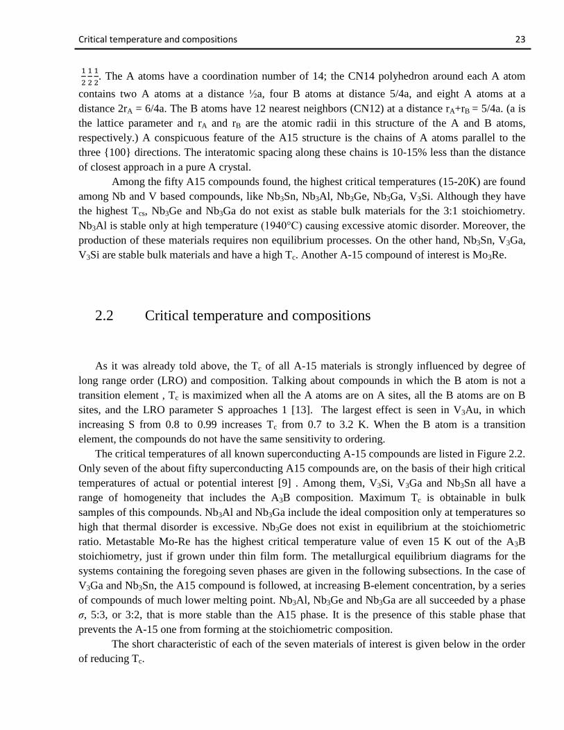
The critical temperatures of all known superconducting A-15 compounds are listed in Figure 2.2.
Only seven of the about fifty superconducting A15 compounds are, on the basis of their high critical
temperatures of actual or potential interest [9] . Among them, V3Si, V3Ga and Nb3Sn all have a
range of homogeneity that includes the A3B composition. Maximum Tc is obtainable in bulk
samples of this compounds. Nb3Al and Nb3Ga include the ideal composition only at temperatures so
high that thermal disorder is excessive. Nb3Ge does not exist in equilibrium at the stoichiometric
ratio. Metastable Mo-Re has the highest critical temperature value of even 15 K out of the A3B
stoichiometry, just if grown under thin film form. The metallurgical equilibrium diagrams for the
systems containing the foregoing seven phases are given in the following subsections. In the case of
V3Ga and Nb3Sn, the A15 compound is followed, at increasing B-element concentration, by a series
of compounds of much lower melting point. Nb3Al, Nb3Ge and Nb3Ga are all succeeded by a phase
σ, 5:3, or 3:2, that is more stable than the A15 phase. It is the presence of this stable phase that
prevents the A-15 one from forming at the stoichiometric composition.
The short characteristic of each of the seven materials of interest is given below in the order
of reducing Tc.
Critical temperature and compositions 24
Figure 2.2. Critical temperatures of binary A15 compounds
known to be superconducting [9].
Nb3Ge (Tc = 23K):
The most striking feature of Nb3Ge phase field is that the stoichiometric composition is not
included at equilibrium, the highest solubility of Germanium being 23 at.%. At 1000°C, the
homogeneity range of the A15 phase is very narrow and is centered at 18 at.% with total width of 1

Critical temperature and compositions 25
at.%. It has not been possible to rise Tc above 17÷18 K in bulk sample either by quenching or other
means. Metastable stoichiometric, or near stoichiometric, Nb3Ge can be prepared as thin films with
critical temperature of 23 K.
The niobium germanium phase diagram is shown in Figure 2.3 [14].
Figure 2.3. The niobium germanium phase diagram
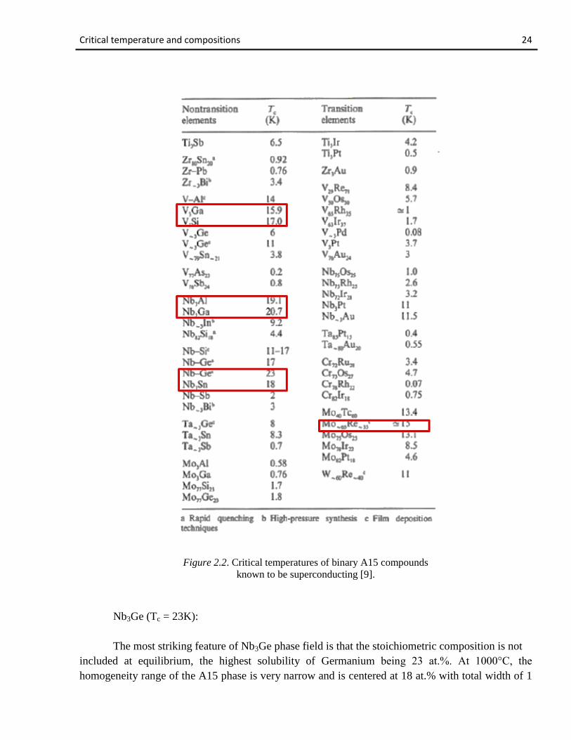
Nb3Ga (Tc = 20,7K)
The A15 phase forms with 21 at.% Ga, by the peritectic reaction at 1860±C. The
stoichiometric composition, 25 at.% Ga, is just attained at 1740±C. Below this temperature the
range of homogeneity narrows rapidly and below 1000±C extends from 19.7 to 20.6 at.% Ga. The
niobium 25allium phase diagram is shown in Figure 2.4 [15].
The “zoomed” version of the A15 phase field, and the critical temperature of samples
corresponding to compositions along the A15-Nb5Ga3 phase boundary are shown in Figure 2.5a,b.
These vary from 9 K for a specimen corresponding to 20.8 at.% Ga to 18 K for 24.3 at.% Ga. Tc for
the latter specimen quenched from 1740±C and subsequently annealed at T < 700±C, which allows
an increase in LRO without precipitation of Nb5Ga3, was 20.7 K.
Nb3Al (Tc = 19,1K)
Critical temperature and compositions 26
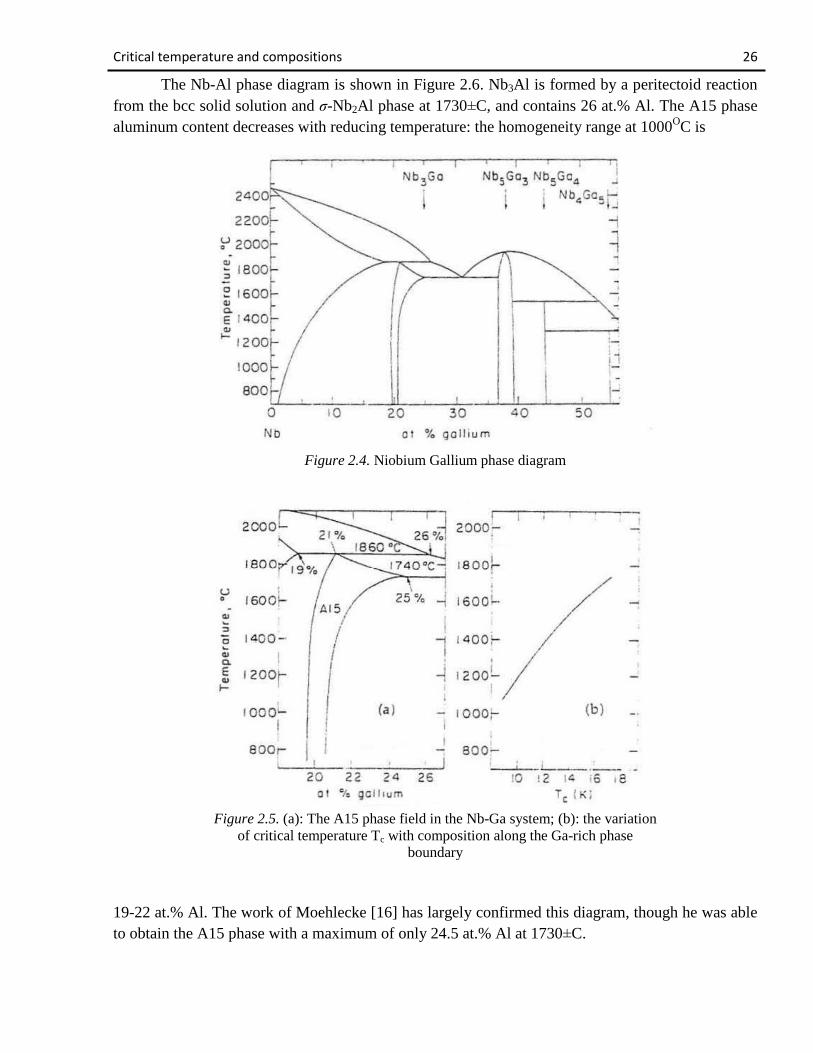
The Nb-Al phase diagram is shown in Figure 2.6. Nb3Al is formed by a peritectoid reaction
from the bcc solid solution and σ-Nb2Al phase at 1730±C, and contains 26 at.% Al. The A15 phase
aluminum content decreases with reducing temperature: the homogeneity range at 1000OC is
Figure 2.4. Niobium Gallium phase diagram
Figure 2.5. (a): The A15 phase field in the Nb-Ga system; (b): the variation
of critical temperature Tc with composition along the Ga-rich phase
boundary
19-22 at.% Al. The work of Moehlecke [16] has largely confirmed this diagram, though he was able
to obtain the A15 phase with a maximum of only 24.5 at.% Al at 1730±C.
Critical temperature and compositions 27
Figure 2.6. Portion of the niobium aluminum phase diagram
Nb3Sn (Tc = 18K)
Nb3Sn is one of the best known high field material among the family of A-15 superconductor
with a Tc of 18.3 K and is used for the production of intense magnetic field reaching a record value
of 21T [17]. The A15 phase for the Nb-Sn intermetallic system is in the composition range of 18 to
25 at.% Sn (see Chapter 4). The superconducting parameters, Tc, Δ, Hc2, depend strongly on the Sn
content [18]. Close to stoichiometry (24.5at.% Sn) and as a result of perfect ordering in the
stoichiometric phase, ρn drops below 20μΩcm. Therefore, RBCS for Nb3Sn has the potential to be
much lower and Q – value much higher than for Nb. More extended information about Nb3Sn see in
the chapter 4.
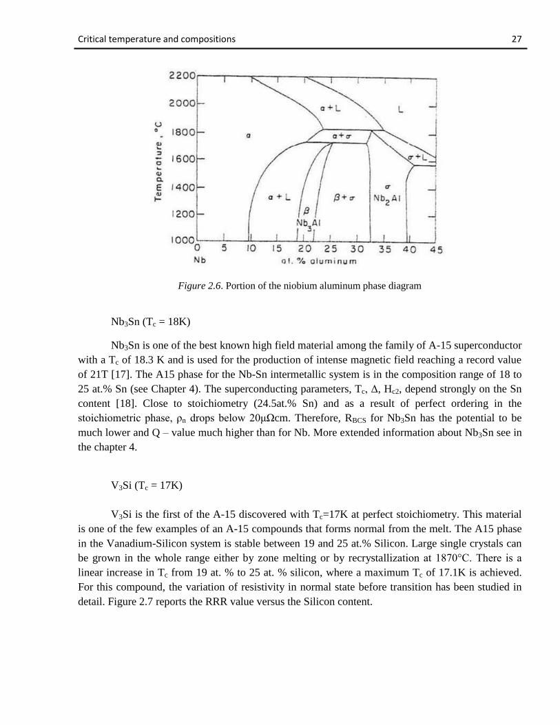
V3Si (Tc = 17K)
V3Si is the first of the A-15 discovered with Tc=17K at perfect stoichiometry. This material
is one of the few examples of an A-15 compounds that forms normal from the melt. The A15 phase
in the Vanadium-Silicon system is stable between 19 and 25 at.% Silicon. Large single crystals can
be grown in the whole range either by zone melting or by recrystallization at 1870°C. There is a
linear increase in Tc from 19 at. % to 25 at. % silicon, where a maximum Tc of 17.1K is achieved.
For this compound, the variation of resistivity in normal state before transition has been studied in
detail. Figure 2.7 reports the RRR value versus the Silicon content.
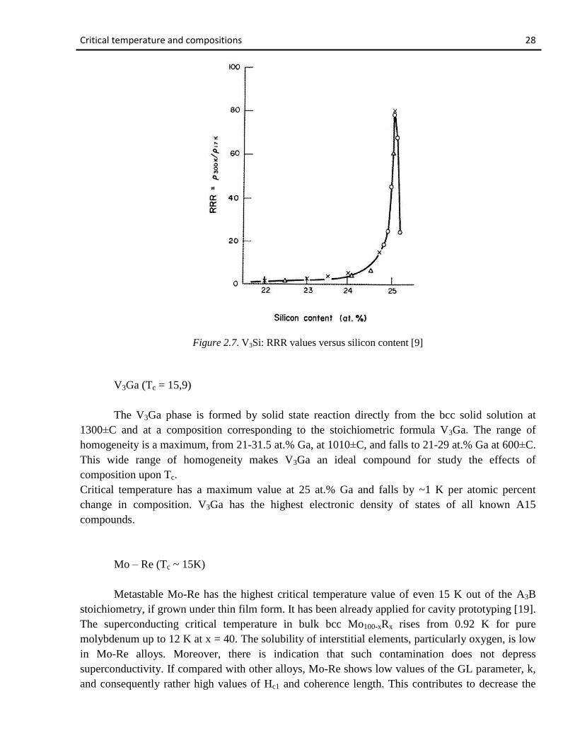
Critical temperature and compositions 28
Figure 2.7. V3Si: RRR values versus silicon content [9]
V3Ga (Tc = 15,9)
The V3Ga phase is formed by solid state reaction directly from the bcc solid solution at
1300±C and at a composition corresponding to the stoichiometric formula V3Ga. The range of
homogeneity is a maximum, from 21-31.5 at.% Ga, at 1010±C, and falls to 21-29 at.% Ga at 600±C.
This wide range of homogeneity makes V3Ga an ideal compound for study the effects of
composition upon Tc.
Critical temperature has a maximum value at 25 at.% Ga and falls by ~1 K per atomic percent
change in composition. V3Ga has the highest electronic density of states of all known A15
compounds.
Mo – Re (Tc ~ 15K)
Metastable Mo-Re has the highest critical temperature value of even 15 K out of the A3B
stoichiometry, if grown under thin film form. It has been already applied for cavity prototyping [19].
The superconducting critical temperature in bulk bcc Mo100-xRx rises from 0.92 K for pure
molybdenum up to 12 K at x = 40. The solubility of interstitial elements, particularly oxygen, is low
in Mo-Re alloys. Moreover, there is indication that such contamination does not depress
superconductivity. If compared with other alloys, Mo-Re shows low values of the GL parameter, k,
and consequently rather high values of Hc1 and coherence length. This contributes to decrease the

Critical temperature and compositions 29
effect of small inhomogeneities by proximity effect. The highest Tc values have been observed for
sputtered films onto substrates held at 1000±C in the composition Mo60Re40 and 1200±C in the
composition Mo38Re62.
Figure 2.8. V3Ga: Vanadium gallium phase diagram
6 GHz cavities 30
3. 6 GHz cavities
3.1 Application
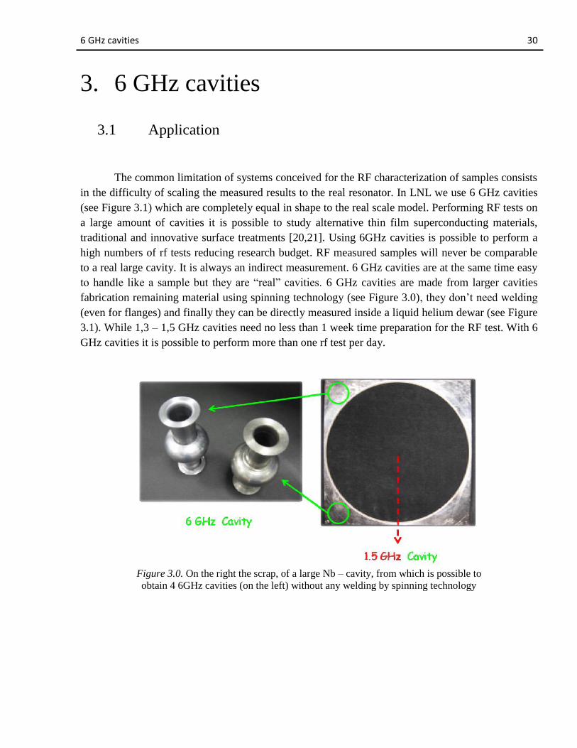
The common limitation of systems conceived for the RF characterization of samples consists
in the difficulty of scaling the measured results to the real resonator. In LNL we use 6 GHz cavities
(see Figure 3.1) which are completely equal in shape to the real scale model. Performing RF tests on
a large amount of cavities it is possible to study alternative thin film superconducting materials,
traditional and innovative surface treatments [20,21]. Using 6GHz cavities is possible to perform a
high numbers of rf tests reducing research budget. RF measured samples will never be comparable
to a real large cavity. It is always an indirect measurement. 6 GHz cavities are at the same time easy
to handle like a sample but they are “real” cavities. 6 GHz cavities are made from larger cavities
fabrication remaining material using spinning technology (see Figure 3.0), they don’t need welding
(even for flanges) and finally they can be directly measured inside a liquid helium dewar (see Figure
3.1). While 1,3 – 1,5 GHz cavities need no less than 1 week time preparation for the RF test. With 6
GHz cavities it is possible to perform more than one rf test per day.
Figure 3.0. On the right the scrap, of a large Nb – cavity, from which is possible to
obtain 4 6GHz cavities (on the left) without any welding by spinning technology
Geometry 31
Figure 3.1. Stand for providing rf-test of 6 GHz cavities
3.2 Geometry.
Figure 3.2. The 6 GHz cavity geometry

Fabrication technique 32
6 GHz cavities are 97 mm long, have a 45 mm diameter cell, an electrical length of 25 mm
and the same shape as a large resonator. It has two large flat flanges at the ends. For each of the
flanges available surface is equal to 7 cm2, in order to ensure the vacuum sealing.
3.3 Fabrication technique
In order to improve the characteristics of the cavity in LNL is used the spinning fabrication
technique. This technology has several advantages in comparison with welding one [22]:
no welding;
short fabrication time;
equipment could be adapted for any size of the cavity, and any quantity of cells;
comparably low fabrication costs;
no intermediate annealing;
almost no scraps;
The process of spinning of the 1,5 GHz cavity is depicted on figure 3.3. But it is also used for
producing 6 GHz Nb – cavities.
Figure 3.3. Producing of the 1,5 GHz cavity by spinning technology
The process is mainly divided in four steps. A circular disk of 400 mm diameter and 3 mm
thickness is first preformed onto a frustum shaped mandrel, then the first half-cell is formed and a
Fabrication technique 33
cylindrical shape is given to the remaining part of the piece, by means of a second pre-mandrel. The
third step consists in spinning the obtained manufact onto a collapsible mandrel that has exactly the
same shape of the cavity interior, up to when the roller overcomes the equator and fixes the piece to
spin onto the mandrel. Then the fourth and last step consists in inserting a further frustum-shaped
collapsible mandrel in order to guide the material when spinning the second half-cell. Both
collapsible mandrels are then removed.
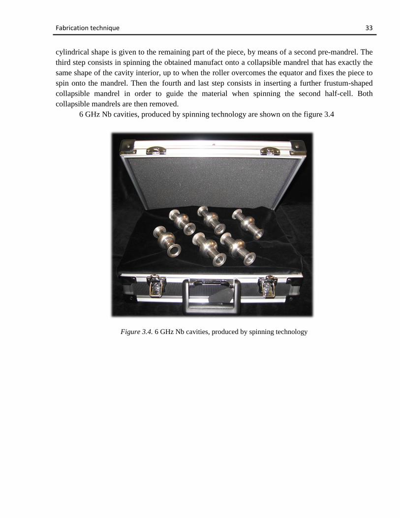
6 GHz Nb cavities, produced by spinning technology are shown on the figure 3.4
Figure 3.4. 6 GHz Nb cavities, produced by spinning technology

Nb3Sn 34
4. Nb3Sn
4.1 Chemical and physical properties
Nb3Sn or triniobium-tin is a metallic chemical compound of niobium (Nb) and tin (Sn), used
industrially as a type II superconductor. This intermetallic compound is a A-15
phases superconductor, and the A15 phase is in the composition range of 18 to 25 at.% Sn. Tc is
equal 18 K. The Niobium-Tin phase diagram is shown on the figure 4.0
Figure 4.0. Niobium – Tin phase diagram
According the diagram on the figure 4.0, the A15 phase is unstable below 930°C. Also, one
can see that there are several spurious phases, and this is a limitation in production of the cavities.
Tc as a function of atomic Sn content 35
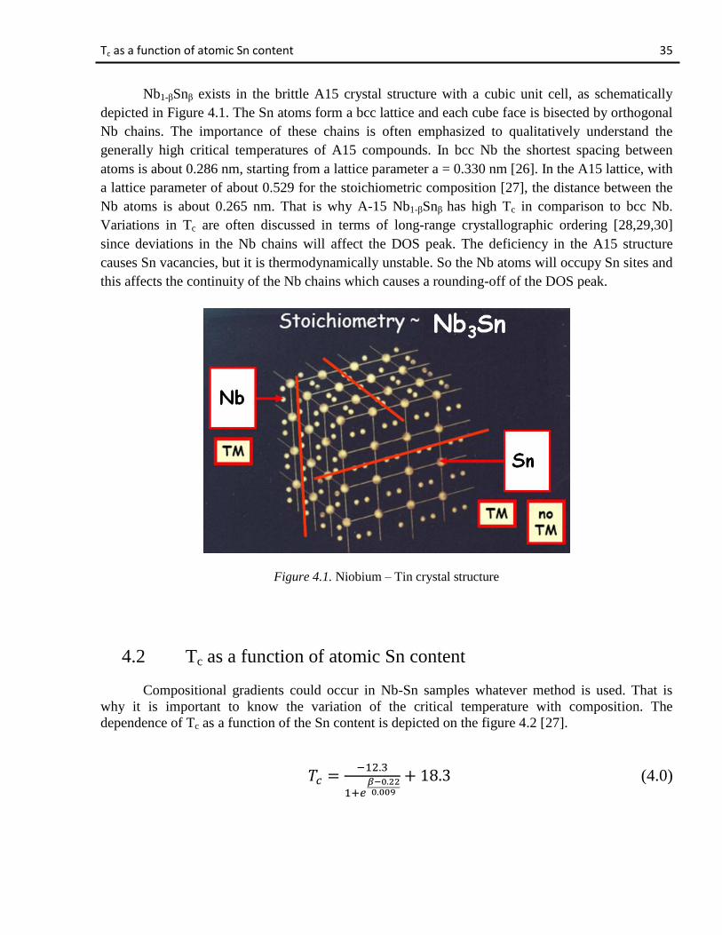
Nb1-βSnβ exists in the brittle A15 crystal structure with a cubic unit cell, as schematically
depicted in Figure 4.1. The Sn atoms form a bcc lattice and each cube face is bisected by orthogonal
Nb chains. The importance of these chains is often emphasized to qualitatively understand the
generally high critical temperatures of A15 compounds. In bcc Nb the shortest spacing between
atoms is about 0.286 nm, starting from a lattice parameter a = 0.330 nm [26]. In the A15 lattice, with
a lattice parameter of about 0.529 for the stoichiometric composition [27], the distance between the
Nb atoms is about 0.265 nm. That is why A-15 Nb1-βSnβ has high Tc in comparison to bcc Nb.
Variations in Tc are often discussed in terms of long-range crystallographic ordering [28,29,30]
since deviations in the Nb chains will affect the DOS peak. The deficiency in the A15 structure
causes Sn vacancies, but it is thermodynamically unstable. So the Nb atoms will occupy Sn sites and
this affects the continuity of the Nb chains which causes a rounding-off of the DOS peak.
Figure 4.1. Niobium – Tin crystal structure
4.2 Tc as a function of atomic Sn content
Compositional gradients could occur in Nb-Sn samples whatever method is used. That is
why it is important to know the variation of the critical temperature with composition. The
dependence of Tc as a function of the Sn content is depicted on the figure 4.2 [27].
(4.0)

Nb3Sn phase formation 36
Equation 4.0 assumes a maximum Tc of 18.3 K, the highest recorded value for Nb3Sn
Figure 4.2. Tc as a function of the Sn content
4.3 Nb3Sn phase formation
The Nb3Sn phase formation occurs through the diffusion process, which doesn’t depend on
the matter state. The diffusion can be described through the Fick's Laws. Fick's first law is used in
steady-state diffusion, i.e., when the concentration within the diffusion volume does not change with
respect to time (Jin = Jout). In one (spatial) dimension, it can be written:
(4.1)

Nb3Sn phase formation 37
where:
J – diffusion flux in dimensions of [
];
D – diffusion coefficient or diffusivity in dimensions of [m2/sec];
ϕ (for ideal mixtures) – concentration in dimensions of [mol/m3];
x – position (length), in dimensions of [m].
D is proportional to the velocity of the diffusing particles, which depends on the temperature,
viscosity of the fluid and the size of the particles according to the Stokes – Einstein relation. In two
or more dimensions we must use the r operator, which generalizes the first derivative, obtaining
(4.2)
The driving force for the one-dimensional diffusion is the quantity
which (for ideal
mixtures) is the concentration gradient. In chemical systems other than ideal solutions or mixtures,
the driving force for diffusion of each species is the gradient of chemical potential of this species.
Then Fick's first law (one - dimensional case) can be written as:
(4.3)
where:
i denote the ith species;
c – concentration (mol/m3);
R – universal gas constant [J/(K mol)];
T – absolute temperature (K);
µ – chemical potential (J/mol).
Fick's second law is used in non-steady or continually changing state diffusion, i.e. when the
concentration within the diffusion volume changes with respect to time.
(4.4)
where:
ϕ – concentration in dimensions of [mol/m3];

Nb3Sn phase formation 38
t – time [s];
D – diffusion coefficient in dimensions of [m2/s];
x – position, [m].
It can be derived from the Fick's First law and the mass balance:
(
) (4.5)
Assuming the diffusion coefficient D to be a constant we can exchange the orders of the
differentiating and multiplying by the constant:
(
)
(4.6)
and, thus, receive the form of the Fick's equations as was stated above. For the case of diffusion in
two or more dimensions the second Fick's Law is:
(4.7)
which is analogous to the heat equation. If the diffusion coefficient is not a constant, but depends
upon the coordinate and/or concentration, the second Fick's Law becomes:
( ) (4.8)
An important example is the case where ϕ is at a steady state, i.e. the concentration does not
change by time, so that the left part of the above equation is identically zero. In one dimension with
constant D, the solution for the concentration will be a linear change of concentrations along x. In
two or more dimensions we obtain:
(4.9)
which is Laplace's equation..
The diffusion coefficient at different temperatures is often found to be well predicted by
(4.10)

Nb3Sn phase formation 39
where:
D – diffusion coefficient;
D0 – maximum diffusion coefficient (at infinite temperature);
EA – activation energy for diffusion;
T – temperature in units of kelvins;
R – gas constant.
An equation having this form is known as the Arrhenius equation. The laws described above
normally apply to the ideal case of two interdiffusing solid species, but in a real situation, we need
to consider the defects role.
Liquid tin diffusion occurs in two distinct steps: the initial simple bulk diffusion and a
second stage characterized by the grain boundary diffusion influence on the growth kinetics. After
the Nb3Sn nucleation, crystallites grow up. The time dependence of the thickness follows a t0,5
low
until the film forms a barrier slowing down the diffusion process. The proposed mechanism is the
intermetallic compound solution – dissolution [126]: this means equilibrium establishing between
Sn diffusing (promoting the layer growing) and the one dissolving back to the liquid.
As one can see from the Nb-Sn phase diagram, the A15 phase stability is guaranteed above
930±C. At a lower temperature the possibility to obtain the formation of spurious phases becomes
concrete.

Inductive annealing fundamentals 40
5. Inductive heating fundamentals
5.1 Introduction
Induction heating is the process of non – contact heating an electrically conducting object (in
our case – 6 GHz superconductive cavity) by electromagnetic induction, where eddy currents are
generated within the metal and resistance leads to Joule heating of the metal. An induction
heater consists of an electromagnet, through which a high-frequency alternating current (AC) is
passed. Heat may also be generated by magnetic hysteresis losses in materials that have
significant relative permeability. The frequency of AC used depends on the object size, material
type, coupling (between the work coil and the object to be heated) and the penetration depth.
Since it is non-contact, the heating process does not contaminate the material being heated. It
is also very efficient since the heat is actually generated inside the cavity. This can be contrasted
with other heating methods where heat is generated in a flame or heating element, which is then
applied to the workpiece. For these reasons Induction Heating lends itself to some unique
applications in science, industry and SRF science in particular.
5.2 Magnetic material properties
Each electron in an atom has a net magnetic moment due to the orbiting and spin. Orbiting
related to the motion of the electron around its nucleus. The orbiting motion of the electron gives
rise to a current loop, generating a very small magnetic field with its moment through its axis of
rotation. Spin can either be in positive (up) direction or in negative (down) direction. Thus each
electron in an atom has a small permanent orbital and spin magnetic moment.
When an external magnetic field H is applied, the magnetic moment in the material tends to
become aligned with this field, resulting in a magnetization of the solid. Assuming a linear relation
between the magnetization vector and the magnetic field makes it possible to write [31, 32]
M = χmH + M0 (5.0)
where
χm – dimensionless quantity called the magnetic susceptibility (a measure of how sensitive a
material is to a magnetic field);
Different kinds of magnetic materials 41
M0 – is a fixed vector that bears no functional relationship to H and is referred to the state of
permanent magnetization.
The magnetic flux density and the magnetic field are related to each other according to
B = μ0(H + M) (5.1)
Combining Eq. (5.0) and (5.1) gives
B = μ0(1 + χm)H + μ0M0 = μ0μrH + μ0M0 = μH + μ0M0 (5.2)
where
μ – permeability of the material
μr – relative permeability, which is given by the permeability of a material over μ0.
5.2.1 Different kinds of magnetic materials
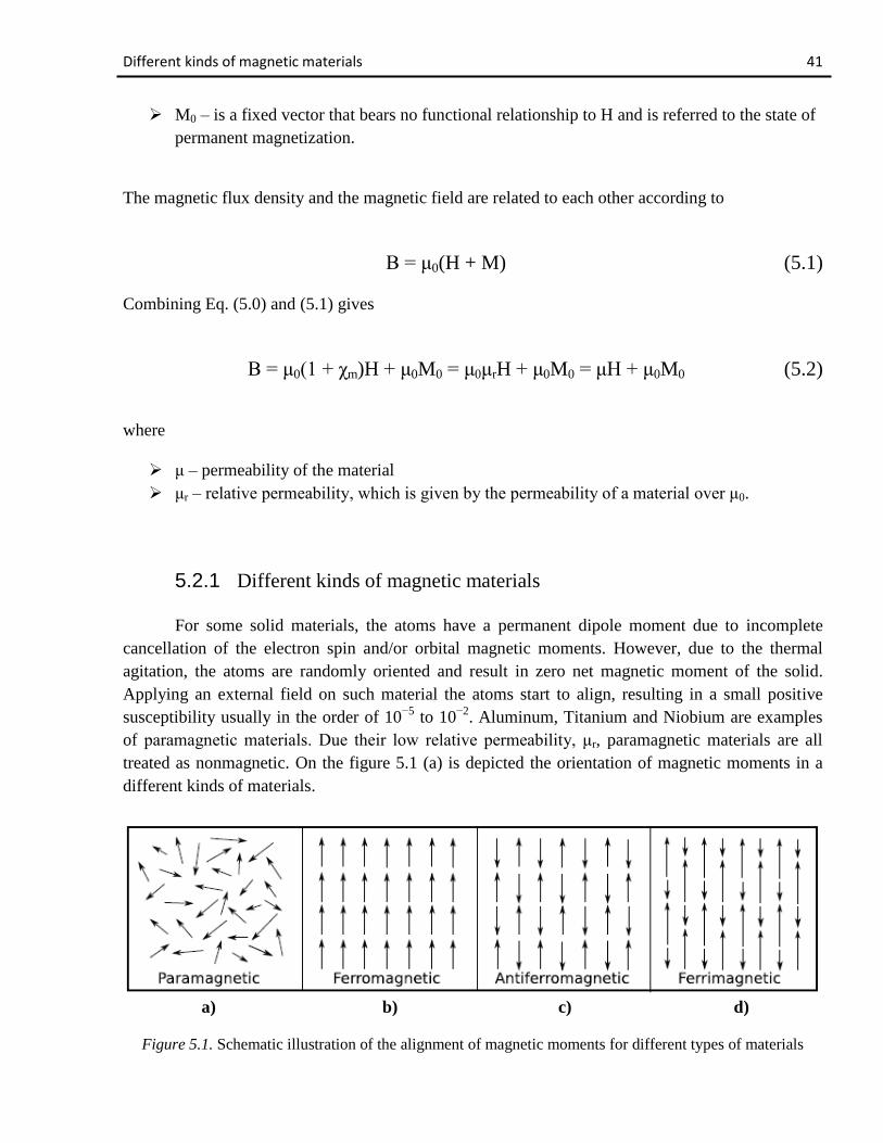
For some solid materials, the atoms have a permanent dipole moment due to incomplete
cancellation of the electron spin and/or orbital magnetic moments. However, due to the thermal
agitation, the atoms are randomly oriented and result in zero net magnetic moment of the solid.
Applying an external field on such material the atoms start to align, resulting in a small positive
susceptibility usually in the order of 10−5
to 10−2
. Aluminum, Titanium and Niobium are examples
of paramagnetic materials. Due their low relative permeability, μr, paramagnetic materials are all
treated as nonmagnetic. On the figure 5.1 (a) is depicted the orientation of magnetic moments in a
different kinds of materials.
a) b) c) d)
Figure 5.1. Schematic illustration of the alignment of magnetic moments for different types of materials
Domains; Hysteresis 42
Ferromagnetic materials have a permanent magnetization even in the absence of a magnetic
field, and is due to the same net atomic magnetic moment as in paramagnetism i.e. electron spins
that do not cancel.
The magnetic moment of an atom in a antiferromagnetic material are antiparallel to the
neighboring atoms, resulting in zero net magnetization. Nickel oxide (NiO), manganese oxide
(MnO) and iron manganese alloy (FeMn) are examples of this material group. A material that
possess such magnetic properties react as if they were paramagnetic.
5.2.2 Domains
A magnetic domain is a region where the individual magnetic moments of the atoms are
aligned with each another. A ferromagnetic or ferrimagnetic material is composed of several
domains, individually changing their alignment. In a polycrystalline specimen the domains do not
correspond with the grain in the material as each grain can consist of more than a single domain.
The magnitude of the magnetization, for the entire solid is therefore the vector sum of the
magnetization for all the domains. In a permanent magnet, the domains stays aligned and the vector
sum is non-zero even in the absence of a magnetic field. Materials that obsess this possibility is
called hard magnetic material. On the other hand, soft magnetic materials are materials that lose
their memory of previous magnetization and can therefore not be a permanent magnetic.
5.2.3 Hysteresis
When a ferromagnetic or ferrimagnetic material is exposed to an externally applied magnetic
field H, the relationship to the magnetic flux density B may not be linear as in Eq. (5.2). A typical
hysteresis curve showing a non-linear relation between B and H and is shown on the figure 5.2.
Initially, domains in the unmagnetized specimen are in different directions. When an external
magnetic field are applied on the specimen, the domains start to line up in the same direction as the
applied magnetic field (figure 5.2 (a), line 1). This orientation process will continue until the
saturation point Bs is reached and all domains are lined up. After this point there is a linear relation
between changes in the magnetic flux and the magnetic field. When the magnetic field is reduced, it
will not follow the initial curve but lags behind (figure 5.2 (a), line 2). This phenomena is called the
hysteresis. Whenever the magnetic field is zero, B is not reduced to zero but to Br. This point is
called the remanence, or remanent flux density; the material remains magnetized in the absence of
an external field. To reduce the magnetic flux in the specimen to zero, a magnetic field of the
magnitude Hc in the opposite direction (to the original one) must be applied (figure 5.2 (b)). Hc is
called the coercive force. The size and shape of the hysteresis curve is of practical importance. The
area within a loop is the energy loss per magnetization cycle which appear as heat that is generated
within the body.

Skin depth 43
a) b)
Figure 5.2. Hysteresis curves. A virgin hysteresis curve (a) and a full hysteresis curve (b)
5.2.4 Skin depth
At high frequency eddy currents are extruded by magnetic field to the surface layers of the
specimen. This is what is called skin – effect. As the result of this extrusion, current density
increases and according to the Joule’s law the specimen heats. The deeper layers of the specimen are
heated due to its thermal conductivity. In the skin layer current density decreases exponentially to
the current density on the surface of the specimen and 85% of heat (relatively to all accumulated
heat) releases in the skin layer. The depth of the skin layer depends on frequency and magnetic
permeability of the metal.
One can calculate the depth of skin layer using next formula:
√ √
√
(5.3)
where:
δ = the skin depth in meters;
μ0 = 4π×10-7
H/m;
μr = the relative permeability of the medium;
ρ = the resistivity of the medium in Ω·m (for Sn = 11,5×10⁻⁸
Ω·m);
f = the frequency of the wave in Hz.
Parallel resonant circuit 44
5.3 Practical implementation of induction heating system
In theory only three things are essential to implement induction heating:
1. A source of High Frequency electrical power;
2. A work coil to generate the alternating magnetic field;
3. An electrically conductive workpiece to be heated.
Having said this, practical induction heating systems are usually a little more complex. For
example, an impedance matching network is often required between the High Frequency source and
the work coil in order to ensure good power transfer. Water cooling systems are also common in
high power induction heaters to remove waste heat from the work coil, its matching network and the
power electronics. Finally some control electronics is usually employed to control the intensity of
the heating action, and time the heating cycle to ensure consistent results. The control electronics
also protects the system from being damaged by a number of adverse operating conditions.
In practice the work coil is usually incorporated into a resonant tank circuit. This has a
number of advantages. As first, it makes either the current or the voltage waveform become
sinusoidal. This minimizes losses in the inverter (which is driving high power and will be described
below) by allowing it to benefit from either zero-voltage-switching or zero-current-switching
depending on the exact arrangement chosen. The sinusoidal waveform at the work coil also
represents a more pure signal and causes less Radio Frequency Interference to nearby equipment.
5.3.1 Parallel resonant tank circuit
The work coil is made to resonate at the particular operating frequency by means of a
capacitor placed in parallel with it (see figure 5.3). This causes the current through the work coil to
be sinusoidal. The parallel resonance also magnifies the current through the work coil, much higher
than the output current capability of the inverter. The inverter “sees” a sinusoidal load current.
However, in this case it only has to carry the part of the load current that actually does real work.
The inverter does not have to carry the full circulating current in the work coil. This property of the
parallel resonant circuit can make a ten times reduction in the current that must be supported by the
inverter and the wires connecting it to the work coil. Conduction losses are typically proportional to
current squared, so a ten times reduction in load current represents a significant saving in conduction
losses in the inverter and associated wiring. This means that the work coil can be placed at a location
remote from the inverter without big losses in the wires.
Work coils using this technique often consist of only a few turns of a thick copper conductor
but with large currents of many hundreds or thousands of amps flowing. (This is necessary to get the
required Ampere turns to do the induction heating.) Water cooling is common for all but the
Impedance matching 45
smallest of systems. This is needed to remove excess heat generated by the passage of the large high
frequency current through the work coil and its associated tank capacitor.
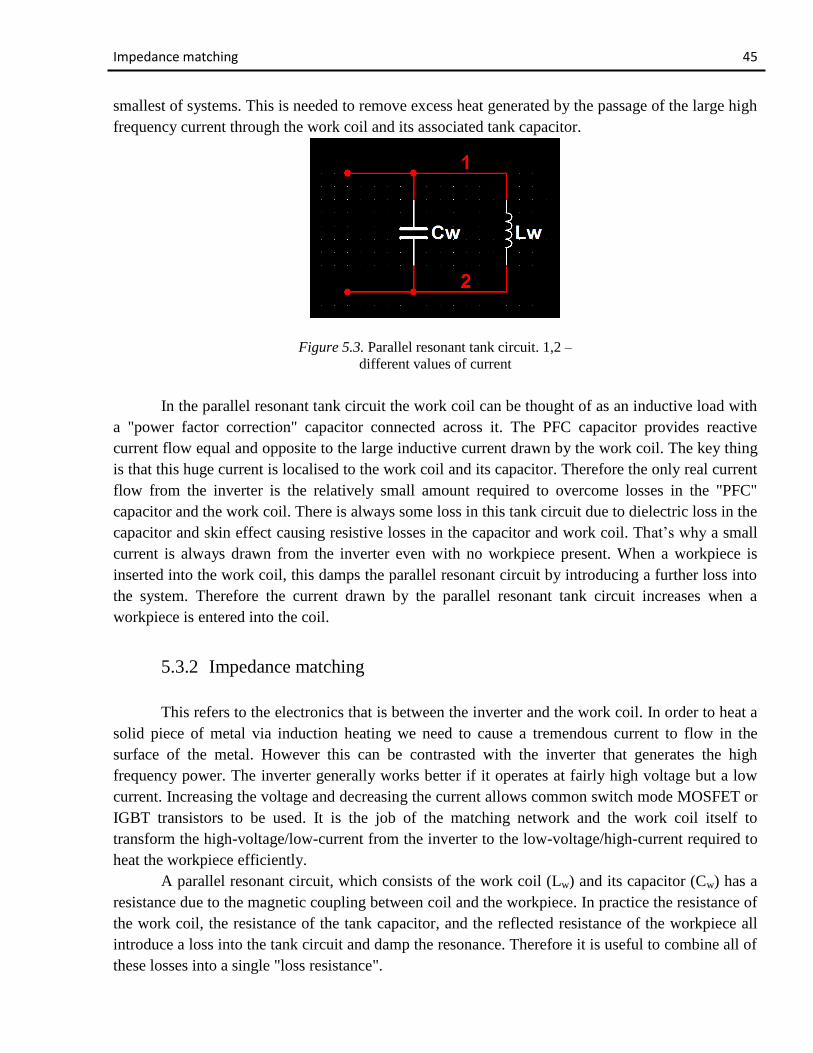
Figure 5.3. Parallel resonant tank circuit. 1,2 –
different values of current
In the parallel resonant tank circuit the work coil can be thought of as an inductive load with
a "power factor correction" capacitor connected across it. The PFC capacitor provides reactive
current flow equal and opposite to the large inductive current drawn by the work coil. The key thing
is that this huge current is localised to the work coil and its capacitor. Therefore the only real current
flow from the inverter is the relatively small amount required to overcome losses in the "PFC"
capacitor and the work coil. There is always some loss in this tank circuit due to dielectric loss in the
capacitor and skin effect causing resistive losses in the capacitor and work coil. That’s why a small
current is always drawn from the inverter even with no workpiece present. When a workpiece is
inserted into the work coil, this damps the parallel resonant circuit by introducing a further loss into
the system. Therefore the current drawn by the parallel resonant tank circuit increases when a
workpiece is entered into the coil.
5.3.2 Impedance matching
This refers to the electronics that is between the inverter and the work coil. In order to heat a
solid piece of metal via induction heating we need to cause a tremendous current to flow in the
surface of the metal. However this can be contrasted with the inverter that generates the high
frequency power. The inverter generally works better if it operates at fairly high voltage but a low
current. Increasing the voltage and decreasing the current allows common switch mode MOSFET or
IGBT transistors to be used. It is the job of the matching network and the work coil itself to
transform the high-voltage/low-current from the inverter to the low-voltage/high-current required to
heat the workpiece efficiently.
A parallel resonant circuit, which consists of the work coil (Lw) and its capacitor (Cw) has a
resistance due to the magnetic coupling between coil and the workpiece. In practice the resistance of
the work coil, the resistance of the tank capacitor, and the reflected resistance of the workpiece all
introduce a loss into the tank circuit and damp the resonance. Therefore it is useful to combine all of
these losses into a single "loss resistance".
Impedance matching 46
When driven at resonance the current drawn by the tank capacitor and the work coil are
equal in magnitude and opposite in phase and therefore cancel each other out as far as the source of
power is concerned. This means that the only load seen by the power source at the resonant
frequency is the loss resistance across the tank circuit. The job of the matching network is simply to
transform this relatively large loss resistance across the tank circuit down to a lower value that better
suits the inverter attempting to drive it. There are many different ways to achieve this impedance
transformation including tapping the work coil, using a ferrite transformer, a capacitive divider in
place of the tank capacitor, or a matching circuit such as an L-match network.
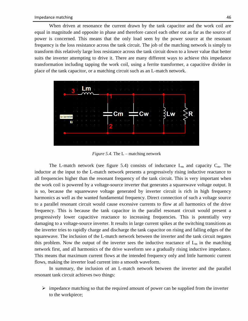
Figure 5.4. The L – matching network
The L-match network (see figure 5.4) consists of inductance Lm and capacity Cm. The
inductor at the input to the L-match network presents a progressively rising inductive reactance to
all frequencies higher than the resonant frequency of the tank circuit. This is very important when
the work coil is powered by a voltage-source inverter that generates a squarewave voltage output. It
is so, because the squarewave voltage generated by inverter circuit is rich in high frequency
harmonics as well as the wanted fundamental frequency. Direct connection of such a voltage source
to a parallel resonant circuit would cause excessive currents to flow at all harmonics of the drive
frequency. This is because the tank capacitor in the parallel resonant circuit would present a
progressively lower capacitive reactance to increasing frequencies. This is potentially very
damaging to a voltage-source inverter. It results in large current spikes at the switching transitions as
the inverter tries to rapidly charge and discharge the tank capacitor on rising and falling edges of the
squarewave. The inclusion of the L-match network between the inverter and the tank circuit negates
this problem. Now the output of the inverter sees the inductive reactance of Lm in the matching
network first, and all harmonics of the drive waveform see a gradually rising inductive impedance.
This means that maximum current flows at the intended frequency only and little harmonic current
flows, making the inverter load current into a smooth waveform.
In summary, the inclusion of an L-match network between the inverter and the parallel
resonant tank circuit achieves two things:
impedance matching so that the required amount of power can be supplied from the inverter
to the workpiece;
LCLR work coil 47
presentation of a rising inductive reactance to high frequency harmonics to keep the inverter
safe.
Looking at the previous schematic above we can see that the capacitor in the matching
network Cm and the tank capacitor Cw are both in parallel. In practice both of these functions are
usually accomplished by a single purpose built power capacitor (figure 5.5). Combing these two
capacitances into one leads us to arrive at the LCLR model for the work coil arrangement, which is
commonly used in industry for induction heating.
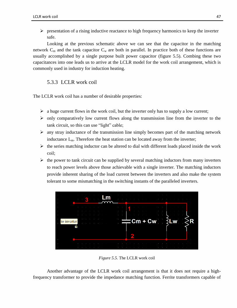
5.3.3 LCLR work coil
The LCLR work coil has a number of desirable properties:
a huge current flows in the work coil, but the inverter only has to supply a low current;
only comparatively low current flows along the transmission line from the inverter to the
tank circuit, so this can use “light” cable;
any stray inductance of the transmission line simply becomes part of the matching network
inductance Lm. Therefore the heat station can be located away from the inverter;
the series matching inductor can be altered to dial with different loads placed inside the work
coil;
the power to tank circuit can be supplied by several matching inductors from many inverters
to reach power levels above those achievable with a single inverter. The matching inductors
provide inherent sharing of the load current between the inverters and also make the system
tolerant to some mismatching in the switching instants of the paralleled inverters.
Figure 5.5. The LCLR work coil
Another advantage of the LCLR work coil arrangement is that it does not require a high-
frequency transformer to provide the impedance matching function. Ferrite transformers capable of

Conceptual schematic 48
handling several kilowatts are large, heavy and quite expensive. In addition to this, the transformer
must be cooled to remove excess heat generated by the high currents flowing in its conductors. The
incorporation of the L-match network into the LCLR work coil arrangement removes the necessity
of a transformer to match the inverter to the work coil, saving cost and simplifying the design.
5.3.4 Conceptual schematic
The system schematic shown on the figure 5.6 is the simplest inverter driving its LCLR work
coil arrangement. This schematic doesn’t show the MOSFET gate-drive circuitry and control
electronics.
Figure 5.6. Half bridge induction heater using LCLR – work coil
The inverter in this demonstration prototype is a simple half-bridge consisting of two
MOSFET transistors. The power is supplied from a smoothed DC supply. The DC-blocking
capacitor is used merely to stop the DC output from the half-bridge inverter from causing current
flow through the work coil. It is sized sufficiently large that it does not take part in the impedance
matching, and does not influence the operation of the LCLR work coil arrangement.
Fault tolerance 49
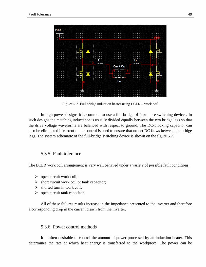
Figure 5.7. Full bridge induction heater using LCLR – work coil
In high power designs it is common to use a full-bridge of 4 or more switching devices. In
such designs the matching inductance is usually divided equally between the two bridge legs so that
the drive voltage waveforms are balanced with respect to ground. The DC-blocking capacitor can
also be eliminated if current mode control is used to ensure that no net DC flows between the bridge
legs. The system schematic of the full-bridge switching device is shown on the figure 5.7.
5.3.5 Fault tolerance
The LCLR work coil arrangement is very well behaved under a variety of possible fault conditions.
open circuit work coil;
short circuit work coil or tank capacitor;
shorted turn in work coil;
open circuit tank capacitor.
All of these failures results increase in the impedance presented to the inverter and therefore
a corresponding drop in the current drawn from the inverter.
5.3.6 Power control methods
It is often desirable to control the amount of power processed by an induction heater. This
determines the rate at which heat energy is transferred to the workpiece. The power can be

Power control methods 50
controlled in a number of different ways. In this work we’ll not go dipply into the electronic part of
power control methods, because it is out of topic, but just represent a list of possible ways:
varying the DC link voltage;
varying the duty ratio of the devices in the inverter;
varying the operating frequency of the inverter;
varying the value of the inductor in the matching network;
impedance matching transformer;
phase-shift control of H-bridge.

Nb3Sn by “double furnace” technique 51
6. Nb3Sn by «double furnace» Liquid Tin
Diffusion fabrication technique
6.1 Introduction
The base idea of the liquid tin diffusion method is introducing the Niobium substrate into a
molten Sn bath and in its subsequent annealing. Method has some advantages in comparison with
other fabrication techniques, such as, for example Tin vapor diffusion or sputtering. This advantages
are:
LTD is a relatively cheap technique (considering the goal is to coat a large number of
cavities, this technique is probably the less expensive one: it employs a low technology
equipment and it is quite fast);
uniformity of the film (stoichiometrically);
can be used for covering surface of wide and complex shaped substrates (!).
we don't need to manipulate dangerous substances as SnCl2 to create a nucleation centers,
and the diffusion process is considerably faster
6.2 Nb3Sn samples fabrication
6.2.1 L-samples
In order to reduce the cost of experiments the L-samples were designed. Samples are made
of Niobium (RRR = 300), has 50 mm long, 20 mm wide and imitates the shape of the cavity as it
shown in the figure 6.0. Each sample has its own number, made by extrusion.
Figure 6.0. Shape of L-sample (a), and number of the sample (b)
Preliminary surface treatments 52
6.2.2 Preliminary surface treatments (mechanical treatment and BCP)
Mechanical treatment
In order to remove scratches caused by Nb-sheets manufacturing, samples have been grinded
using different particle sizing SiC abrasive papers. The idea is to have the same starting surface for
the chemical polishing. Typically the chosen sequence begins with a 600 grained paper and finish
with a soft cloth to remove the possible residual particulate. During the process, a water flow is
continuously refreshing the substrates to avoid their worming up. At the end of the described
mechanical treatment, the Nb pieces were washed in ultrasonic with Rodaclean for 60 minutes,
cleaned with acetone and alcohol and after dried.
Chemical treatment
Following the classical surface treatments after the mechanical polishing the procedure
counts a chemical polishing. Chemical treatments are performed to smooth further on the sample
surface, to remove the possible niobium oxides and contaminants. The used solution is the acid
mixture containing HF 40%, HNO3 65% and H3PO4 85% (standard Buffered Chemical Polishing,
BCP 1:1:2). Nitric acid plays the niobium surface oxidizing role. Hydrofluoric acid reduces the
niobium pentaoxide into a salt that is soluble in water. Phosphoric acid acts as a moderator for the
chemical reaction giving rise to a less turbulent and more controllable reaction (see Equations 6.0,
6.1 and 6.2).
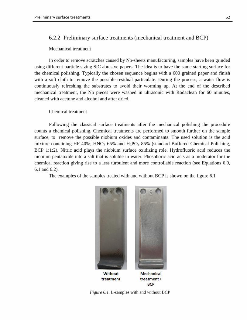
The examples of the samples treated with and without BCP is shown on the figure 6.1
Figure 6.1. L-samples with and without BCP
Glow discharge 53
6Nb(s) + 10HNO3(aq) → 3Nb2O5(s) + 10NO(gas) + 5H2O(l) (6.0)
Nb2O5(s) + 6HF(aq) → H2NbOF5(aq) + NbO2F(s) ∙
H2O +
H2O(l) (6.1)
NbO2F(s) ∙
H2O + 4HF(aq) → H2NbOF5(aq) +
H2O(l) (6.2)
6.2.3 Glow Discharge
Part of the samples, in order to increase cleanness of the surface were treated with use of
vacuum plasma discharge in the glow regime. The goal was to obtain extremely clean surface in
order to improve diffusion of Tin into Niobium and reduce the residual Tin droplets (see chapter
5.3.8).
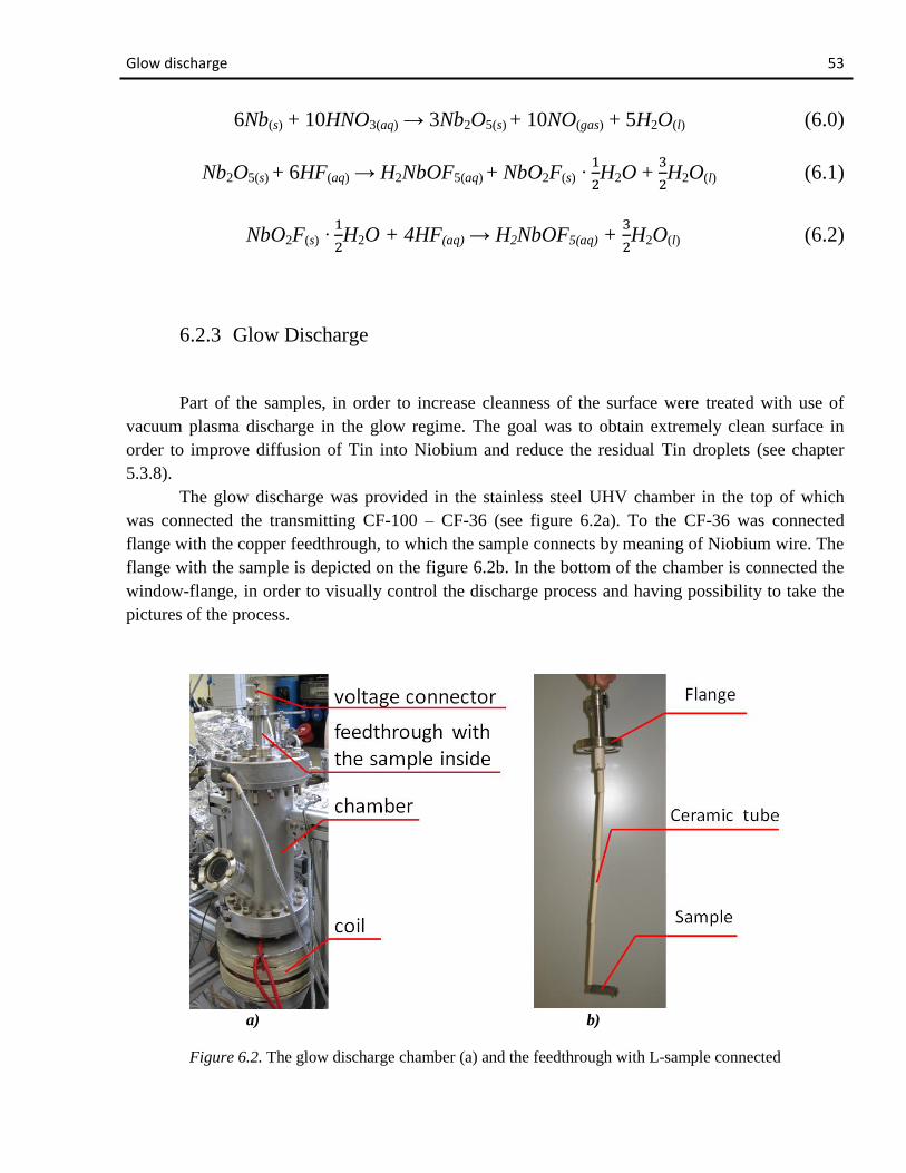
The glow discharge was provided in the stainless steel UHV chamber in the top of which
was connected the transmitting CF-100 – CF-36 (see figure 6.2a). To the CF-36 was connected
flange with the copper feedthrough, to which the sample connects by meaning of Niobium wire. The
flange with the sample is depicted on the figure 6.2b. In the bottom of the chamber is connected the
window-flange, in order to visually control the discharge process and having possibility to take the
pictures of the process.
a) b)
Figure 6.2. The glow discharge chamber (a) and the feedthrough with L-sample connected

Glow discharge 54
Niobium-wire feedthrough was insulated by the ceramic tubes, in order to prevent discharge
of the wire. With the aim of uniform discharge of all of the sample planes we fixed it in a horizontal
position, otherwise (in vertical position) the magnetic field is perpendicular to the bended part of the
sample and this plane doesn’t discharge.
The pumping unit is made of a rotary TriScroll (12.6 m3/h) pump and a turbomolecular
pump (70 l/s), and has a pneumatic gauge, mount in the inlet of turbomolecular pump for preventing
damage of the pump while venting and opening the chamber and a whole-metal valve for
disconnecting the chamber from the main chamber (i.e. glow discharge camber is a part of the
system, contain of four chambers). Also there are the argon inlet, controlled by a leak valve for
regulating the process pressure in the chamber, controlled by a leak valve, and the nitrogen inlet for
venting the chamber, controlled by a leak valve.
The magnetic field was provided by means of the external coil, connected to tension-
stabilized source. Relationship between the current, flowing through the coil and inducted magnetic
field is shown on the figure 6.3
Figure 6.3. Relationship between the current, supplied to the coil and
inducted magnetic field
Parameters of the glow discharge process are reported in the table 6.1
base pressure 1,65∙10-8
mBar
baking time 16 hours
baking temperature 120OC
process gas Nitrogen
glow discharge pressure 10-3
mBar
cathode current 0,04 A
magnetic field 525 Gauss
Table 6.1. Glow discharge parameters
Anodization 55
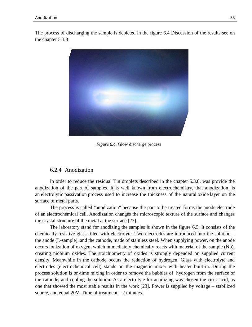
The process of discharging the sample is depicted in the figure 6.4 Discussion of the results see on
the chapter 5.3.8
Figure 6.4. Glow discharge process
6.2.4 Anodization
In order to reduce the residual Tin droplets described in the chapter 5.3.8, was provide the
anodization of the part of samples. It is well known from electrochemistry, that anodization, is
an electrolytic passivation process used to increase the thickness of the natural oxide layer on the
surface of metal parts.
The process is called "anodization" because the part to be treated forms the anode electrode
of an electrochemical cell. Anodization changes the microscopic texture of the surface and changes
the crystal structure of the metal at the surface [23].
The laboratory stand for anodizing the samples is shown in the figure 6.5. It consists of the
chemically resistive glass filled with electrolyte. Two electrodes are introduced into the solution –
the anode (L-sample), and the cathode, made of stainless steel. When supplying power, on the anode
occurs ionization of oxygen, which immediately chemically reacts with material of the sample (Nb),
creating niobium oxides. The stoichiometry of oxides is strongly depended on supplied current
density. Meanwhile in the cathode occurs the reduction of hydrogen. Glass with electrolyte and
electrodes (electrochemical cell) stands on the magnetic mixer with heater built-in. During the
process solution is on-time mixing in order to remove the bubbles of hydrogen from the surface of
the cathode, and cooling the solution. As a electrolyte for anodizing was chosen the citric acid, as
one that showed the most stable results in the work [23]. Power is supplied by voltage – stabilized
source, and equal 20V. Time of treatment – 2 minutes.

Anodization 56
a) b)
Figure 6.5. Anodization laboratory stand (a) and the L-sample after
anodization treatment(b)
6.2.5 Chemical etching
Another kind of treatment, that has been tried in order to increase the purity of the sample
surface was the chemical etching. For etching we decide to use the same solution as for BCP (HF
40%, HNO3 65% and H3PO4 85%), but without the ortophosphoric acid, which is normally used as a
buffering agent controlling the rate of etching. When introducing the sample to the solution we were
observing the high rate reaction, with a big amount of brown gas (NO3) producing. The rate of
reaction grows exponentially with the increasing the temperature. Material erosion becomes too
violent and heat evolution makes the solution to boil in 3 minutes.
Process of the chemical etching is depicted in the figure 6.6

Experimental apparatus for dipping 57
Figure 6.6. Chemical etching process
6.2.6 Experimental apparatus for dipping
Experimental apparatus, that was used for producing the Nb3Sn layer over the
superconductive 6 GHz Nb cavities and Nb samples is depicted on the figure 6.7. The high vacuum
cylindrical reaction chamber is made of Inconel: it is a Ni-Cr-Fe alloy chosen because of its stability
at the high process temperature, that we have to reach. It contains an Alumina crucible with the Tin
inside (99.99% nominal purity) (Figure 6.8 (a)). The Al2O3 vessel extraction can be done through a
long metallic rod which can be hooked up to the Inconel cooling jacket that encloses the crucible.
The vacuum chamber has a Chromel-Alumel thermocouple, which monitors temperature in the zone
between the chamber wall and the alumina vessel. A pneumatic gauge, mount in the inlet of
turbomolecular pump for preventing damage of the pump while venting and opening the chamber.
Also there are the nitrogen inlet for venting the chamber, controlled by a leak valve.
The pumping unit is made of a rotary TriScroll (12.6 m3/h) pump and a turbomolecular
pump (70 l/s). A UHV linear manipulator permits us to move the samples (cavity) from the top to
the bottom (and vice versa) and to rotate them around the chamber principle axis. To avoid
contaminations, the support for the samples is made of niobium (Figure 6.8 (b)).
The chamber (it’s lower part) can be heated by an resistive furnace (hot zone) while, to avoid
Sn vapor condensation in the manipulator and in the pumping systems, the upper section ("cold
zone") can be cooled with a water jacket.
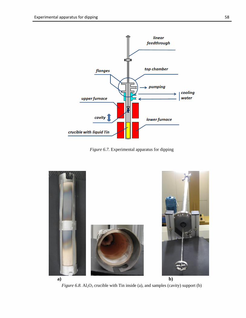
Experimental apparatus for dipping 58
Figure 6.7. Experimental apparatus for dipping
a) b)
Figure 6.8. Al2O3 crucible with Tin inside (a), and samples (cavity) support (b)
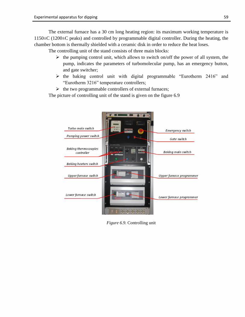
Experimental apparatus for dipping 59
The external furnace has a 30 cm long heating region: its maximum working temperature is
1150±C (1200±C peaks) and controlled by programmable digital controller. During the heating, the
chamber bottom is thermally shielded with a ceramic disk in order to reduce the heat loses.
The controlling unit of the stand consists of three main blocks:
the pumping control unit, which allows to switch on/off the power of all system, the
pump, indicates the parameters of turbomolecular pump, has an emergency button,
and gate switcher;
the baking control unit with digital programmable “Eurotherm 2416” and
“Eurotherm 3216” temperature controllers;
the two programmable controllers of external furnaces;
The picture of controlling unit of the stand is given on the figure 6.9
Figure 6.9. Controlling unit

Experimental apparatus for dipping 60
Figure 6.10. Photograph of the liquid tin
diffusion experimental stand
6.2.7 Dipping of L-samples
Samples were fixed on the support by means of Niobium wires in order to avoid
contaminations (see figure 6.11)
Figure 6.11. The way to fix the samples on the support

Experimental apparatus for dipping 61
Measuring the distance between the manipulator flange end the samples, and knowing the Sn
level in the chamber, it becomes easy to calculate the necessary displacements to position the
sample inside the liquid bath, in the hot zone or in the cold one. Below it is shown the calculations.
ρ1(Sn) = 7.365 g/cm3 (room temperature)
ρ2(Sn) = 6.99 g/cm3 (liquid)
cm
cm
3
ρ1V1 = ρ2V2 →
(cm
3)
cm
cm
After samples were fixed, and closed inside, the chamber is evacuated until p < 5∙10-6
mBar.
This process usually takes 2-3 hours. Before starting dipping, in order to degas the surface of the
chamber, a baking process was provided. Usually it's about twelve hours long: temperature of the
system, during baking process is maintained at 120OC. After baking, when the experimental
apparatus cools down, its pressure reaches the order of 10-9
– 10-10
mBar. And this pressure is a
basic for starting dipping.
Figure 6.12. L – samples after dipping
Resistive furnace annealing 62
The dipping step simply consists in the substrate lowering inside liquid tin through the linear
manipulator motion: it has been done for various combinations of T and time. Samples were
preheated in the annealing zone before dipping. In this fabrication technique is not anticipated
opening the chamber between dipping and annealing steps, that’s why it is impossible to represent
results of the dipping step before annealing of all samples. Only four samples were taken out just
after dipping in order to see the uniformity of the film, and the picture of this samples is represented
in the figure 6.12.
6.2.8 Resistive furnace annealing
In order to anneal the samples, resistive furnace is preliminary heated up to 1050OC. It is the
maximum temperature, which is limited by the melting point of Inconel – chamber and the fact, that
over this temperature, the process of hydrogen diffusion through the wall of the chamber becomes
extremely fast, and this hydrogen contaminates the samples (cavity), what is very undesirable. After
dipping step, by meaning of moving up the manipulator, samples are transported into annealing zone
for the preliminary estimated time of annealing (4 – 24 hours).
After annealing samples are moved up to the cold zone (which is cooled by water inside the
cooling jacket) in order to fix the phase of obtained film. And finally, all the system is cooled down
to the room temperature (it takes about 10 hours), pumping stops, the chamber vents with Nitrogen
in order to prevent adsorbing of air inside the chamber walls and samples, end the samples are taken
out of system.
6.2.9 Obtained films and problem of residual Tin droplets
The most representative results of the obtained films, and the regimes of producing are
shown on the table 6.2.
of the
sample
Preliminary
surface treatment
Time of
dipping,
min
Temperature
of dipping, OC
Time of
annealing,
min
Temperature
annealing, OC
1-1 alcohol + acetone
cleaning
10 min 1050 12 hours 1050
2-1 BCP
10 min
10 min 1050 12 hours 1050
3-1 BCP
10 min + glow
discharge
1 min
10 min 1050 12 hours 1050

Resistive furnace annealing 63
4-1 BCP 10 min +
glow discharge 2
min
10 min 1050 12 hours 1050
1-2 BCP
10 min
2 min 1050 4 hours 1050
2-2 BCP
10 min +
anodization
2 min 1050 4 hours 1050
3-2 chemical etching 2 min 1050 4 hours 1050
4-2 glow discharge 2 min 1050 4 hours 1050
Table 6.2. Obtained films on the L – samples by LTD with resistive furnace annealing
Pictures of the samples are represented on the figures 6.13 and 6.14 Numbers of the samples
corresponds to same on the table 6.2.
Figure 6.13. L – samples covered with Nb3Sn with different surface treatments
techniques
The main problem, which we were dialed with in this research was the problem of non-
uniform coating of the sample after dipping step – a droplet of Tin on the band part of the sample
and the residual Tin after annealing.
As one can see from the pictures, each sample has a problem of residual unreacted Tin on the
surface, especially on the band part of the sample. From the obtained results we can make the
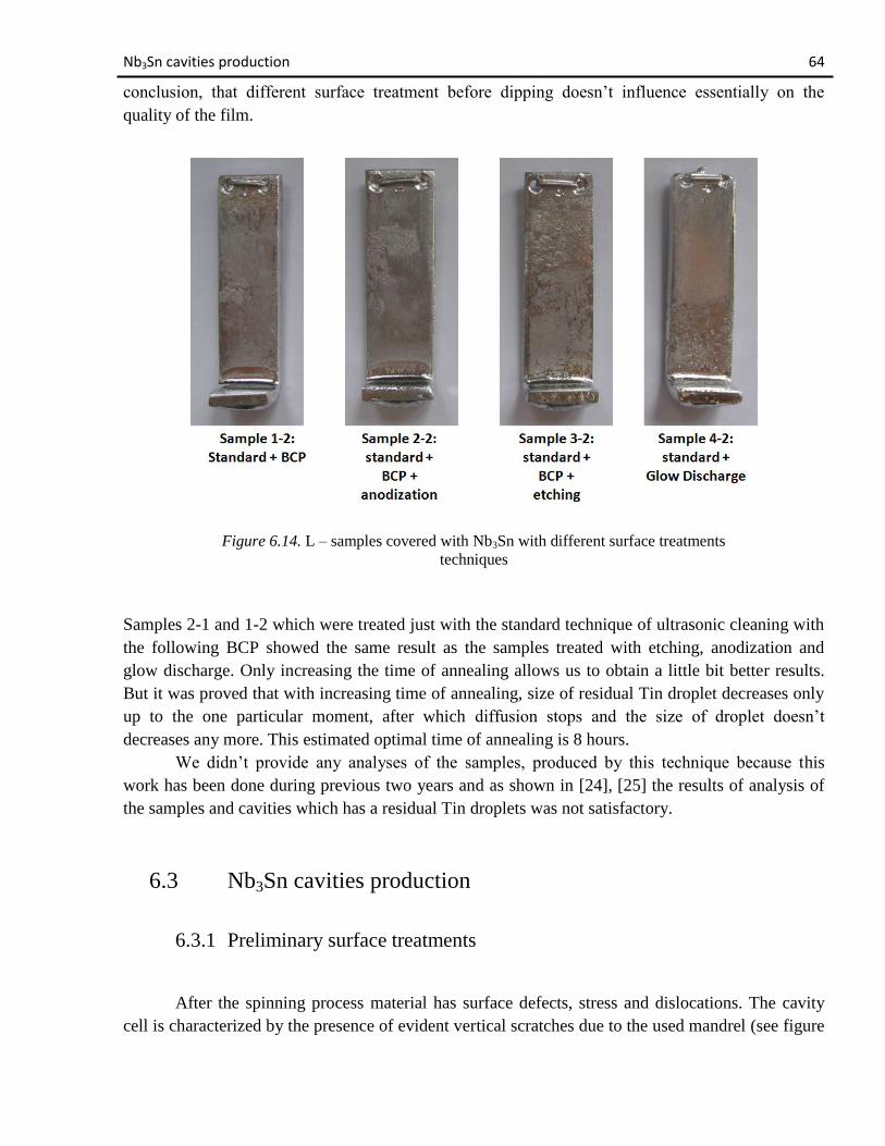
Nb3Sn cavities production 64
conclusion, that different surface treatment before dipping doesn’t influence essentially on the
quality of the film.
Figure 6.14. L – samples covered with Nb3Sn with different surface treatments
techniques
Samples 2-1 and 1-2 which were treated just with the standard technique of ultrasonic cleaning with
the following BCP showed the same result as the samples treated with etching, anodization and
glow discharge. Only increasing the time of annealing allows us to obtain a little bit better results.
But it was proved that with increasing time of annealing, size of residual Tin droplet decreases only
up to the one particular moment, after which diffusion stops and the size of droplet doesn’t
decreases any more. This estimated optimal time of annealing is 8 hours.
We didn’t provide any analyses of the samples, produced by this technique because this
work has been done during previous two years and as shown in [24], [25] the results of analysis of
the samples and cavities which has a residual Tin droplets was not satisfactory.
6.3 Nb3Sn cavities production
6.3.1 Preliminary surface treatments
After the spinning process material has surface defects, stress and dislocations. The cavity
cell is characterized by the presence of evident vertical scratches due to the used mandrel (see figure
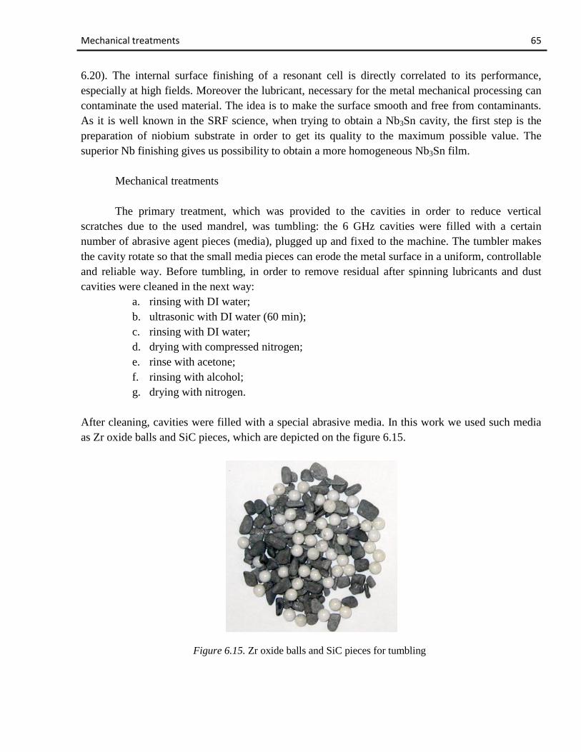
Mechanical treatments 65
6.20). The internal surface finishing of a resonant cell is directly correlated to its performance,
especially at high fields. Moreover the lubricant, necessary for the metal mechanical processing can
contaminate the used material. The idea is to make the surface smooth and free from contaminants.
As it is well known in the SRF science, when trying to obtain a Nb3Sn cavity, the first step is the
preparation of niobium substrate in order to get its quality to the maximum possible value. The
superior Nb finishing gives us possibility to obtain a more homogeneous Nb3Sn film.
Mechanical treatments
The primary treatment, which was provided to the cavities in order to reduce vertical
scratches due to the used mandrel, was tumbling: the 6 GHz cavities were filled with a certain
number of abrasive agent pieces (media), plugged up and fixed to the machine. The tumbler makes
the cavity rotate so that the small media pieces can erode the metal surface in a uniform, controllable
and reliable way. Before tumbling, in order to remove residual after spinning lubricants and dust
cavities were cleaned in the next way:
a. rinsing with DI water;
b. ultrasonic with DI water (60 min);
c. rinsing with DI water;
d. drying with compressed nitrogen;
e. rinse with acetone;
f. rinsing with alcohol;
g. drying with nitrogen.
After cleaning, cavities were filled with a special abrasive media. In this work we used such media
as Zr oxide balls and SiC pieces, which are depicted on the figure 6.15.
Figure 6.15. Zr oxide balls and SiC pieces for tumbling
Mechanical treatments 66
Cavities, with the media inside, were closed with the special plastic flanges, with use of the
rubber o-rings, and fixed inside the support by means of the plastic clamps (see figures 6.16, 6.17).
Figure 6.16. 6 GHz cavity and the plastic flange with o-ring
Figure 6.17. Filled with the media cavities fixed in a tumbling support
And finally the support with cavities inside was placed into the drum cavity holder of the
tumbler, depicted on the figure 6.18, 6.19.
Mechanical treatments 67
Figure 6.18. Tumbler drawing
Figure 6.19. Photograph or the tumbler

Mechanical treatments 68
The tumbling parameters for the 6 GHz cavities are presented on the table 6.3. The speed of
the media was calculated with use of next formula:
(6.3)
were:
Vmedia - velocity of the media sliding on cavity wall;
- angular velocity of media inside cavity;
- radius of the cavity.
Tumbler Rotary Speed
200 RPM
f = 3,3 Hz
ω = 20,7
300 RPM
f = 5 Hz
ω = 31,4
Vmedia [m/s]
On Equator
R2 = 0,02 m
0,4 0,6
Vmedia [m/s]
On Tube
R2 = 0,01 m
0,2 0,3
Fmedia [N]
Mass = 0,005 Kg
R1 = 0,24 m
0,5 1,2
Table 6.3. Tumbling parameters for the 6 GHz cavities
The pictures of the internal surface of the cavity cell-part were taken with use of the special
mini-camera, which allows to take pictures with different angle corresponding to the zero-angle
(zero angle corresponds to the position of the cavity, when it’s number, extruded on the cut-off part
is in the lowest point). The picture of the mini-camera and the results of cavity – tumbling is
presented on the figure 6.20.

Chemical treatments 69
Figure 6.20. Mini-camera for taking pictures of the internal surface of the cavity and
the results of 6GHz cavity tumbling (cell-part)
After all mechanical operations follows cavities flanges preparation. Flanges surface must be
flat and polished to prevent leaks on cavities rf testing stand. For this aim we used polishing circle
with different abrasive papers wetted with water. First is paper 400 for rough treatment which
produces flat surface. Next will go 600, 800, 1000 which will decrease roughness. Final is 1200 with
using alcohol instead of water. After lapping is necessary to make precise washing of cavity in
ultrasound bath with soap in few steps and rinsing.
Chemical treatments
The procedure and solution for 6GHz cavities BCP is the same that for Nb L-samples (see
chapter 5.2.2). But the chemical treatment is performed in a pulsed way using a closed circuit. In the
static case, a buffer layer forms the concentration gradient in the solution - metal surface zone and
H2 evolution limit the reaction rate. Hydrogen bubbles, which are not evacuated from the cavity cell
reduce the rate of chemical reaction. In the pulsed system, the acid flux is directed from the bottom
to the top of the cavity in order evacuate the hydrogen, produced during the process. The 3-way
valves are used for inversion the flux direction. Stand for pulsed BSP is represented on the figure
6.21.
Dipping 70
Figure 6.21. Stand for pulsed BSP of 6 GHz cavity
Pictures of the internal surface of the cavity before and after BCP are shown on the figure
6.22.
a) b)
Figure 6.22. Internal surface of the cavity-cell part before (a) and after (b) BCP
6.3.2 Dipping.
For dipping cavities the same experimental stand that for samples was used. Cavities were
fixed on the bottom edge of the linear feedthrough with use of Niobium wire in special way, which
limits the movement of the cavity. The picture of the cavity, fixed on the feedthrough is shown on
the figure 6.23.

Resistive furnace annealing 71
Figure 6.23. The way to fix the cavity on the support
After cavity is fixed, and closed inside, the chamber is evacuated until p < 5∙10-6
mBar. This
process usually takes 2-3 hours. Before starting dipping, in order to degas the surface of the
chamber, a baking process was provided. Usually it's about twelve hours long: temperature of the
system, during baking process is maintained at 120OC. After baking, when the experimental
apparatus cools down, its pressure reaches the order of 10-9
– 10-10
mBar. And this pressure is a
basic for starting dipping.
The dipping step simply consists in the substrate lowering inside liquid tin through the linear
manipulator motion: it has been done for various combinations of T and time.
6.3.3 Resistive furnace annealing
For annealing of each cavity, resistive furnace is preliminary heated up to 1050OC. After
dipping step, by meaning of moving up the manipulator, cavity is transported into annealing zone
for the preliminary estimated time of annealing (4 – 24 hours). All limitations of the resistive
furnace were described in the chapter 5.2.8.
After annealing cavity is moved up to the cold zone (which is cooled by water inside the
cooling jacket) in order to fix the phase of obtained film and avoid possible formation of spurious
phases such as Nb6Sn5 or NbSn2 that one can see on the Nb – Sn diagram. And finally, all the
system is cooled down to the room temperature (it takes about 10 hours), pumping stops, the
chamber vents with Nitrogen to prevent adsorbing of air inside the chamber walls and cavity, and
the cavity is taken out of system.

Obtained coatings 72
6.3.4 Obtained coatings
List of the cavities that were done with parameters of process is represented on the table 6.4.
As one can see from the table, for some cavities we provide also the pre-heating step, but the long
exposure to Sn vapors, at low temperature, could promote spurious phase formations, so soon we
decline this step.
of the
cavity
Tpre-heat, OC
tpre-heat, hours
Tdipping, OC
tdipping, min
Tanneal1, OC
tanneal1, hours
Tanneal2, OC
tanneal2, hours
Droplets of
Tin
1 300
3
1050
10
1050
4
1050
24
yes
2 1000
1
1050
5
1050
4
/ yes
3 1000
1
1050
5
1050
10
/ yes
Table 6.4. Parameters and results of coating 6 GHz cavities
The main problem of the of the method applied to the 6 GHz cavities was still the presents of
droplets of unreacted residual tin. The most problematic zones of the cavity one can see on the
figure 6.24.
Figure 6.24. Zones of the highest concentration of unreacted Tin on the
6 GHz cavity surface (Tin is marked by the red color)

Obtained coatings 73
As shown on the picture, the main zones, where droplets of Tin are concentrated, are on the
horizontal planes, because the layer of Sn there is the thickest after dipping step.
In the case of first cavity, after first annealing, the droplets of residual Tin were still present
on the internal and external surfaces. So it was decided to provide the second extra- long time
annealing (24 hours), in order to estimate possibility of removing residual Tin by slow evaporation
at 1050OC. Pictures of the external and internal surface of the first cavity are represented below.
Cavity 1 after first annealing (figure 6.25):
a) b)
c)
Figure 6.25. External surface of the cavity 1 after first annealing. Tin accumulation on the
upper part of the cell (a), clear lower part of the cell (b) and the layer of Tin on the lower
flange (c)
And the same cavity after second annealing is represented on the figure 6.26.
Obtained coatings 74
a) b)
c) d)
Figure 6.26. External surface of the cavity 1 after first annealing. Tin accumulation on the upper part of the
cell (a), upper flange and the support (b) and the layer of Tin on the lower flange (c), (d)
The second and third cavities were made with one – step annealing, 4 and 10 hours
correspondingly. But for this cavities the temperature of pre heating was increased to 1000OC. The
pictures of this cavities are presented on the figures 6.27 and 6.28.
a) b)
Figure 6.27. External surface of the cavity 2 after annealing. Tin accumulation on the
upper part of the cell (a), and the lower flange (b)

Obtained coatings 75
a) b)
c)
Figure 6.28. External surface of the cavity 3 after annealing. Tin accumulation on the upper
part of the cell (a), lower part of the cell is clear (b), and the lower flange (b) is covered with the
layer of Tin
6.4 Nb3Sn 6 GHz cavities analysis
6.4.1 Internal surface pictures by mini – camera
Because of the resonator small dimensions the 6 GHz internal surface inspection is quite
complex. 6 GHz cavities have been observed through a miniature camera (which is described in the
chapter 5.3.1) to check the material surface after each performed operation: a series of photographs
can be easily taken to monitor the internal surface of the cavity. On the picture 6.29 is represented
the pictures of the cavity 1 internal surface.

RF - test 76
Figure 6.29. Internal surface of the cavity 1 after first annealing. Accumulation of residual Tin on the
different parts of the cavity.
As one can see from the figure 6.29, the Tin droplets problem is particularly evident:
droplets are present on the both cut-off part (less) and especially the cell bottom and iris parts.
6.4.2 RF - test
The work of measuring Qvalue of the cavities which has droplets of residual Tin inside was
done for previous 3 years [24], and it was absolutely proved, that cavities with residual Tin doesn’t
show a good Qvalue. So, in order to economy time and materials, we didn’t provide rf – tests of the
cavities with residual Tin, because the result was wittingly bad. As an example, here is shown one of
results of measuring the Qvalue of the cavity with Nb3Sn film and residual Tin droplets in comparison
with pure Niobium cavity, which was treated just mechanically and BCP (figure 6.30). As one can
see from the plot, the Qvalue of treated cavity is one order of magnitude worth, than pure Niobium
cavity.

RF - test 77
Figure 6.30. Results of measuring the Qvalue of the cavity with Nb3Sn film and residual Tin
droplets in comparison with pure Niobium cavity, which was treated just mechanically and BCP

N3Sn by LTD with high-temperature annealing 78
7. Nb3Sn by LTD with high-temperature
annealing
After a lot of work, that has been done during 3 years in the Liquid Tin Diffusion method we
understood that the only one way to solve the problem of residual Tin droplets is rising the
temperature of annealing in order to improve the diffusion of Tin into Niobium, and evaporate all
residuals. The base idea of the liquid tin diffusion method with high – temperature inductive
annealing is the same as for standard LTD technique: introducing the Niobium substrate into a
molten Sn bath and in its subsequent annealing. But the high temperature annealing gives some
advantages in comparison with standard resistive furnace annealing. This advantages are:
the maximum temperature, that can be reached is much higher than the temperature of
resistive furnace and lies in the range of 1900 – 2100OC;
time for heating the cavity (or the sample) from 0 to 1500OC is less than 3 minutes;
no diffusion of the contaminations through the wall of the chamber, because it stays
relatively cold;
chamber doesn’t heats during the annealing so it becomes possible to use stainless steel as a
material for chamber;
technique doesn’t require cooling of the chamber;
7.1 Nb3Sn samples production
7.1.1 L – samples and LL – samples
For producing Nb3Sn coating by LTD with high-temperature annealing were used two kind
of samples: the L – samples and the so called LL – samples. L – samples were described in detail on
the chapter 6.2.1. The LL – samples carries out the same role that L – samples, but they are smaller
in dimensions and consequently easier for analysing. Samples are made of Niobium, has 20 mm
long, 10 mm wide and has the LL – shape as shown on the picture 7.1. Each sample has its own
number, made by extrusion.
Figure 7.1. The LL – sample
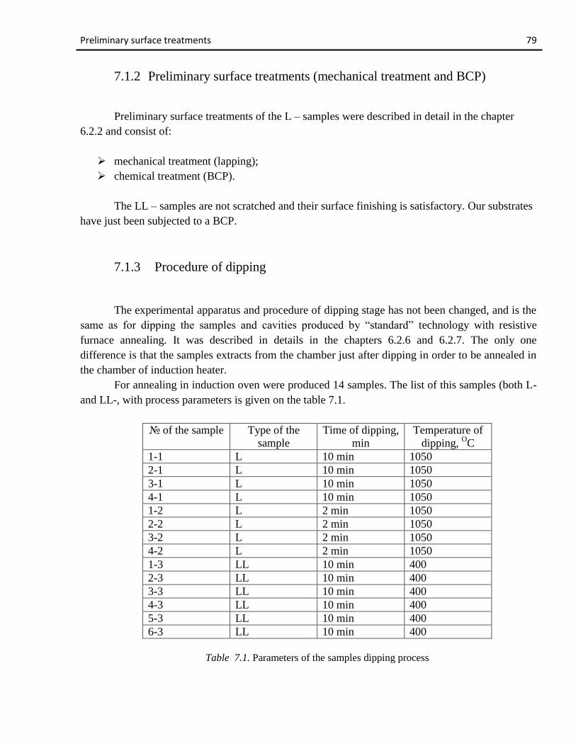
Preliminary surface treatments 79
7.1.2 Preliminary surface treatments (mechanical treatment and BCP)
Preliminary surface treatments of the L – samples were described in detail in the chapter
6.2.2 and consist of:
mechanical treatment (lapping);
chemical treatment (BCP).
The LL – samples are not scratched and their surface finishing is satisfactory. Our substrates
have just been subjected to a BCP.
7.1.3 Procedure of dipping
The experimental apparatus and procedure of dipping stage has not been changed, and is the
same as for dipping the samples and cavities produced by “standard” technology with resistive
furnace annealing. It was described in details in the chapters 6.2.6 and 6.2.7. The only one
difference is that the samples extracts from the chamber just after dipping in order to be annealed in
the chamber of induction heater.
For annealing in induction oven were produced 14 samples. The list of this samples (both L-
and LL-, with process parameters is given on the table 7.1.
of the sample Type of the
sample
Time of dipping,
min
Temperature of
dipping, OC
1-1 L 10 min 1050
2-1 L 10 min 1050
3-1 L 10 min 1050
4-1 L 10 min 1050
1-2 L 2 min 1050
2-2 L 2 min 1050
3-2 L 2 min 1050
4-2 L 2 min 1050
1-3 LL 10 min 400
2-3 LL 10 min 400
3-3 LL 10 min 400
4-3 LL 10 min 400
5-3 LL 10 min 400
6-3 LL 10 min 400
Table 7.1. Parameters of the samples dipping process

Inductive annealing experimental apparatus 80
The film, that was obtained as the result of dipping stage is depicted in the figure 7.2. As one
can see from the picture, film is not uniform, with the presence of the droplets of Tin, especially in
the corners. And this picture is representative for all produced samples after the dipping stage. From
this we can resume, that the most important stage, that influence on the quality of Nb3Sn film,
produced by LTD is annealing.
Figure 7.2. Film obtained as the result of dipping on LL – samples
7.1.4 Inductive annealing experimental apparatus
For inductive annealing both the samples and the 6 GHz cavities was specially designed a
new experimental apparatus which is depicted on the figure 7.3. It consist of the two main parts:
vacuum system and inductor.
The high vacuum cylindrical reaction chamber is made of stainless steel. In this case we
don’t need using Inconel, because the chamber stays relatively cold during the process. It contains a
7 – rings copper inductor work coil (Figure 7.4 (a)). The vacuum chamber has a Chromel-Alumel
thermocouple, which monitors it’s temperature. Inductor chamber connected to the main vacuum
chamber through the whole – metal valve. A pneumatic gauge, mount in the inlet of turbomolecular
pump for preventing damage of the pump while venting and opening the chamber. Also there is the
nitrogen inlet for venting the chamber, controlled by a leak valve.
The pumping unit is made of a rotary TriScroll (12.6 m3/h) pump and a turbomolecular
pump (70 l/s). A UHV linear manipulator, connected to the upper flange of the chamber permits

Inductive annealing experimental apparatus 81
moving the samples (cavity) up and down in the range of 50 mm in order to find the best position
inside the work coil while preparing the chamber to experiment. To avoid contaminations, the
support for the samples is made of niobium (Figure 7.4 (a)).
Figure 7.3. Inductive annealing stand
1-manipulator; 2-vacuum chamber; 3-whole metal valve; 4-window flange; 5-
pneumatic gauge; 6-turbomolecular pump; 7-gauge switcher; 8-inlet of work
coil; 9-pump controller; 10-baking control unit; 11-induction heater
controlling and inverter block; 12-inductor main switcher; 13-tank capacitors
block; 14-pressure indicator.
Vacuum chamber has a window flange which needed for precise displacing the samples
inside the work coil, and for visual control of the annealing process. As it is well known from the
theory the inductor main coil must be well insulated from the chamber. That’s why in this system
we use the lower flange (through which work coil enters the chamber) with the ceramic insulator.
During annealing inside the chamber creates the atmosphere of evaporated Tin, which
sedimentates to the walls and bottom of the chamber. To prevent short circuit of the inlet and outlet

Inductive annealing experimental apparatus 82
tubes of the work coil by sedimentated Tin we decide to use the ZrO2 balls. The capacity of the
lower flange is filled with this balls as shown on the figure 7.4 (b). After each experiment the balls
are mixed, and so we can use the one “charge” of balls for 3-5 annealings. After balls are totally
covered by Tin, they can de recovered by chemical etching and used again and again.
a) b)
Figure 7.4. Lower flange with work coil (a) and the ZrO2 balls in the lower flange
capacity (b).
1-Nb samples/cavity support; 2-work coil; 3-cavity; 4-flange; 5-cooling water
inlet/outlet
The inductor that is used in our research is the EKOHEAT Model 10C 300-0771. It contains
two main blocks: The power control block (11, figure 7.3), and the parallel resonant circuit content
of tank capacitors block (work head, 13, figure 7.3) which is connected to the copper work coil (2,
figure 7.4). Work coil made with the shape which follows the shape of the cavity for improving the
uniform heating. Power control block is made on the two inverters build on the power IGBT, and
has programmable interface. Tank capacitor block has summary capacitance of 2µF with 1000 VRMS
voltage. Here are listed some important features of the inductor heating system:
efficient heating of many part geometries (either samples or cavities);
agile operation for repeatable, reliable results;
touch – pad interface for control and programming;
backlight LCD display for indicating data;
electrically isolated water-cooled work head.

Inductive annealing procedure 83
The power can be controlled using one of following ways:
manually from the front panel;
remotely by the signals provided to the rear panel;
remotely through the RS-485 serial communication port;
from one of 10-step heating profiles specified in advance.
The parameters of the inductor are represented on the table 7.2.
Feature Value Units
Power supply
Dimensions H×D×W 432×616×451 mm
Construction aluminum
Weight 32 kg
Input AC Voltage 360-520 VRMS
Input Frequency 50-60 Hz
AC Line Power 11 kVA max
Power Factor 0.92
Output Frequency 50-150 kHz
RF Output Voltage 1020 VRMS max
Output Power 10 kW max
Work head
Dimensions H×D×W 229×203×457 mm
Mounting M6×1×12 screws (8×)
Weight 20 kg
Total capacitance 2 µF
Voltage 1000 VRMS max
Work coil
Material copper
Number of rings 7
Cooling water
Table 7.2. Parameters of the induction oven
7.1.5 Inductive annealing procedure
After finishing the dipping step, samples are mounted to the inductive annealing chamber.
For fixing the samples on the support is used Niobium wire, as shown on the figure 7.5. After
samples were fixed, and closed inside, the chamber is evacuated until p < 5∙10-6
mBar. This process
usually takes 1-1,5 hours. Before starting annealing, in order to degas the surface of the chamber
and improve vacuum, a baking process is provided. Usually it's about twelve hours long:
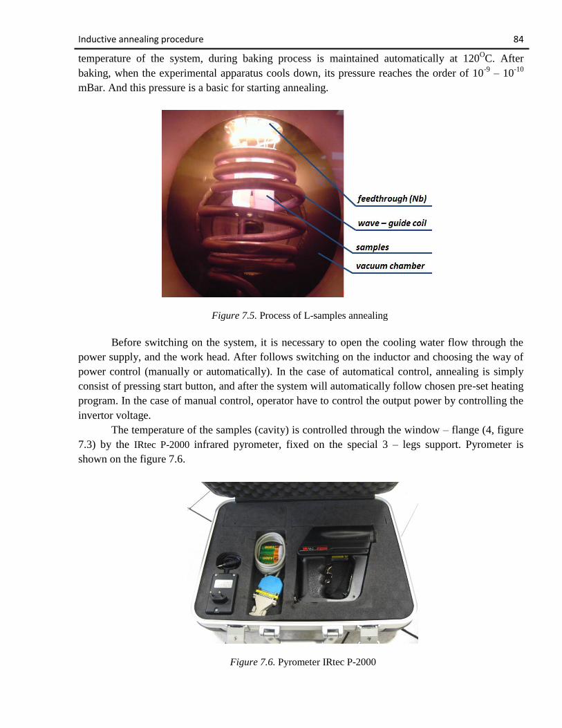
Inductive annealing procedure 84
temperature of the system, during baking process is maintained automatically at 120OC. After
baking, when the experimental apparatus cools down, its pressure reaches the order of 10-9
– 10-10
mBar. And this pressure is a basic for starting annealing.
Figure 7.5. Process of L-samples annealing
Before switching on the system, it is necessary to open the cooling water flow through the
power supply, and the work head. After follows switching on the inductor and choosing the way of
power control (manually or automatically). In the case of automatical control, annealing is simply
consist of pressing start button, and after the system will automatically follow chosen pre-set heating
program. In the case of manual control, operator have to control the output power by controlling the
invertor voltage.
The temperature of the samples (cavity) is controlled through the window – flange (4, figure
7.3) by the IRtec P-2000 infrared pyrometer, fixed on the special 3 – legs support. Pyrometer is
shown on the figure 7.6.
Figure 7.6. Pyrometer IRtec P-2000

Obtained films 85
Using this instrument permits measurement of the temperature starting from 500OC. But in
fact, during the annealing process the window is progressively metalises with the Tin, and
measurement firstly becomes not correct, and after totally impossible. That is why we were trying to
estimate the quality of the Nb3Sn film as a function of output inverter voltage, but not of
temperature.
7.1.6 Obtained films
The regimes of samples annealing are represented on the tables 7.3 (L-samples 1-2, 2-2, 3-2,
4-2); 7.4 (LL-samples 1-3, 2-3, 3-3, 4-3, 5-3, 6-3). The frequency in all cases was constant and
equals 85 kHz.
Output
voltage, V
Output power,
kW
Pressure,
mBar
approximate
temperature, OC
time of step,
min
100 0,7 1×10⁻⁵ // 1
200 2,2 1,1×10⁻⁵ 1118 1
250 3,3 9,3×10⁻⁶ 1320 1
300 4,6 2,6×10⁻⁵ 1500 2
Total Time of annealing, min 5
Table 7.3. Annealing parameters of the L-samples 1-2, 2-2, 3-2, 4-2
The photograph of the L-samples 1-2, 2-2, 3-2, 4-2 is represented on the figure 7.7.
Figure 7.7. The photograph of the L-samples 1-2, 2-2, 3-2, 4-2 after annealing in the
induction oven
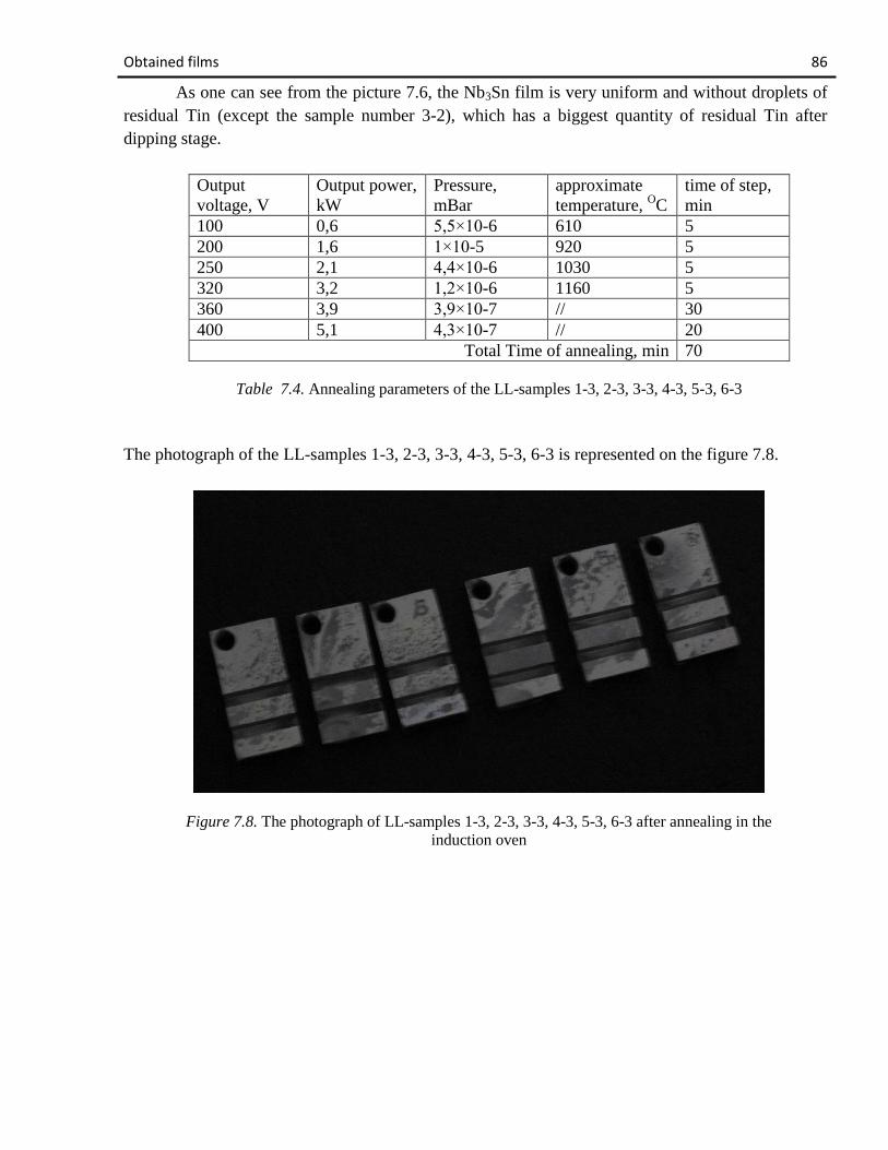
Obtained films 86
As one can see from the picture 7.6, the Nb3Sn film is very uniform and without droplets of
residual Tin (except the sample number 3-2), which has a biggest quantity of residual Tin after
dipping stage.
Output
voltage, V
Output power,
kW
Pressure,
mBar
approximate
temperature, OC
time of step,
min
100 0,6 5,5×10⁻⁶ 610 5
200 1,6 1×10⁻⁵ 920 5
250 2,1 4,4×10⁻⁶ 1030 5
320 3,2 1,2×10⁻⁶ 1160 5
360 3,9 3,9×10⁻⁷ // 30
400 5,1 4,3×10⁻⁷ // 20
Total Time of annealing, min 70
Table 7.4. Annealing parameters of the LL-samples 1-3, 2-3, 3-3, 4-3, 5-3, 6-3
The photograph of the LL-samples 1-3, 2-3, 3-3, 4-3, 5-3, 6-3 is represented on the figure 7.8.
Figure 7.8. The photograph of LL-samples 1-3, 2-3, 3-3, 4-3, 5-3, 6-3 after annealing in the
induction oven

Nb3Sn samples analysis 87
7.2 Nb3Sn samples analysis
The Nb3Sn samples we obtained are described. The instruments that were used for samples
analysing are: X-ray diffractometer to examine the crystal structures of the samples, a inductive
(phase shift) system to evaluate Tc and ΔTc. Below are reported the results of the samples analysing.
7.2.1 XRD measurements
The X-ray diffraction analysis is extremely useful to have information about the obtained
material crystal structure and plane orientations. Furthermore it is possible to detect the eventual
presence of undesired species.
The instrument at our disposal is a diffractometer "X'Pert-Pro" (produced by the Philips
company). The X-ray beam wavelength is 0.15428 nm (Cu Kα). During scanning the incident beam
is fixed at a small angle (calculated respect to the sample surface) while the detector rotate
depending on the parameters chosen through the software (mainly start and stop angles and
acquisition time). Changing the operation mode it is possible to increase the examined penetration
depth (both beam source and detector move, one towards the other). The XRD spectra have been
acquired for the most of the samples.
On the pictures 7.9, 7.10 is shown the bulk scan and the thin film scan typical spectra of
obtained coatings on the samples, produced by LTD with inductive annealing.
Figure 7.9. The bulk scan XRD spectra of the sample, produced by LTD with annealing in the
induction oven

XRD measurements 88
As it is seen from the XRD spectra, all of the peaks are associated to the Nb3Sn A15 phase,
confirming the method of LTD with inductive annealing as the very encouraging technique that
must be developed more and more.
Figure 7.10. The thin film scan XRD spectra of the sample, produced by LTD with annealing in
the induction oven
7.2.2 Inductive Tc and ΔTc measurement
Measuring Tc and ΔTc in this work was done with use of inductive method. The method
makes use of the perfect shielding of a magnetic field by a superconducting thin film carrying
subcritical current densities only. This technique implicates using of a two – coil arrangement,
which is shown on the figure 7.11. Samples were cooling down with the liquid helium, by dipping
the set up into the helium tank.
The results of measuring Tc and ΔTc on the LL – samples are represented on the table 7.5.

Inductive Tc and ΔTc measurements 89
Figure 7.11. Two coil arrangement of the inductive Tc set up
Number of
the sample
Theoretical
value
1 2 3 4 5 6
Tc1, K 18,2 17,91 17,89 17,88 17,90 17,90 17,80
ΔTc1 // 0,07 0,06 0,04 0,06 0,06 0,12
Tc2, K 9,2 9,31 9,27 9,27 9,30 9,28 9,28
ΔTc2 // 0,01 0,01 0,01 0,01 0,02 0,01
Table 7.5. Results of measuring Tc and ΔTc on the LL – samples
7.3 Nb3Sn 6 GHz cavities production
7.3.1 Preliminary surface treatments
The goal of the cavity preliminary surface treatments is to make the internal surface smooth
and free from contaminants. As it is well known in the SRF science, when trying to obtain a Nb3Sn
cavity, the first step is the preparation of niobium substrate in order to get its quality to the
maximum possible value. All the cavities, before depositing the film were treated mechanically
(tumbling) and chemically (BCP) as described in the chapter 6.3.1.
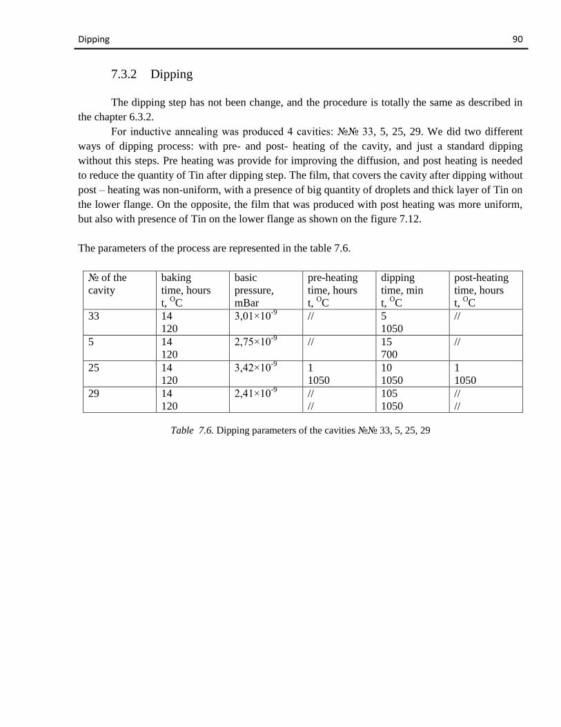
Dipping 90
7.3.2 Dipping
The dipping step has not been change, and the procedure is totally the same as described in
the chapter 6.3.2.
For inductive annealing was produced 4 cavities: 33, 5, 25, 29. We did two different
ways of dipping process: with pre- and post- heating of the cavity, and just a standard dipping
without this steps. Pre heating was provide for improving the diffusion, and post heating is needed
to reduce the quantity of Tin after dipping step. The film, that covers the cavity after dipping without
post – heating was non-uniform, with a presence of big quantity of droplets and thick layer of Tin on
the lower flange. On the opposite, the film that was produced with post heating was more uniform,
but also with presence of Tin on the lower flange as shown on the figure 7.12.
The parameters of the process are represented in the table 7.6.
of the
cavity
baking
time, hours
t, OC
basic
pressure,
mBar
pre-heating
time, hours
t, OC
dipping
time, min
t, OC
post-heating
time, hours
t, OC
33 14
120
3,01×10⁻⁹
// 5
1050
//
5 14
120
2,75×10⁻⁹
// 15
700
//
25 14
120
3,42×10⁻⁹
1
1050
10
1050
1
1050
29 14
120
2,41×10⁻⁹
//
//
105
1050
//
//
Table 7.6. Dipping parameters of the cavities 33, 5, 25, 29

Inductive annealing 91
a) b)
Figure 7.12. Cavity after dipping step. Cavity 5 (a) produced without post heating,
and cavity 25 (b) produced with post heating
7.3.3 Inductive annealing
Inductive annealing is the most important step in the LTD technique. The advantages of
inductive annealing in comparison with resistive furnace annealing are evident: it is non-contact
treatment, the heating process does not contaminate the material being heated. It is also very
efficient since the heat is actually generated inside the cavity. This can be contrasted with other
heating methods where heat is generated in a flame or heating element, which is then applied to the
workpiece.
Procedure of inductive annealing was described in details above, in the chapters 7.1.4, 7.1.5.
In the case of annealing the cavity, it was also like a samples, fixed on the support with Niobium
wires, as shown on the figures 7.4 (a), 7.13. Power of the heater was regulated manually. All
treatments was provide on the output inductor frequency of 85 kHz. Estimated experimentally
relating between the output voltage and the temperature of the cavity is shown on the figure 7.14.

Inductive annealing 92
Figure 7.13. Cavity fixed on the support for annealing
Figure 7.14. Relation between the output inductor voltage and the temperature of the cavity
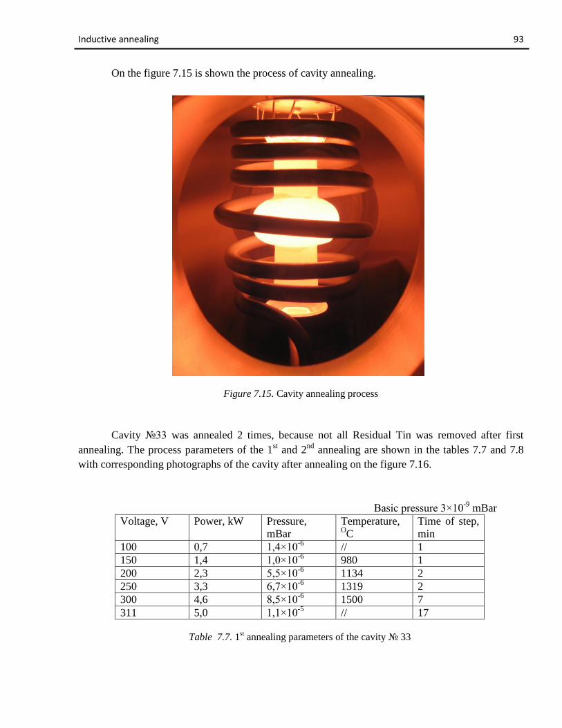
Inductive annealing 93
On the figure 7.15 is shown the process of cavity annealing.
Figure 7.15. Cavity annealing process
Cavity 33 was annealed 2 times, because not all Residual Tin was removed after first
annealing. The process parameters of the 1st and 2
nd annealing are shown in the tables 7.7 and 7.8
with corresponding photographs of the cavity after annealing on the figure 7.16.
Basic pressure 3×10⁻⁹
mBar
Voltage, V Power, kW Pressure,
mBar
Temperature, OC
Time of step,
min
100 0,7 1,4×10⁻⁶
// 1
150 1,4 1,0×10⁻⁶
980 1
200 2,3 5,5×10⁻⁶
1134 2
250 3,3 6,7×10⁻⁶
1319 2
300 4,6 8,5×10⁻⁶
1500 7
311 5,0 1,1×10⁻⁵
// 17
Table 7.7. 1st annealing parameters of the cavity 33

Inductive annealing 94
Basic pressure 7,5×10⁻⁹
mBar
Voltage, V Power, kW Pressure,
mBar
Temperature, OC
Time of step,
min
100 0,7 1,1×10⁻⁶
// 1
150 1,4 6,7×10⁻⁶
900 2
200 2,3 2,6×10⁻⁶
1128 2
250 3,3 3,2×10⁻⁶
1310 2
300 4,6 3,2×10⁻⁶
1485 2
350 6,3 4,9×10⁻⁵
1670 2
388 7,6 6,6×10⁻⁵
1800 10
Table 7.8. 2nd
annealing parameters of the cavity 33
after dipping after 1
st annealing after 2
nd annealing
Figure 7.16. Results of annealing cavity 33
On the table 7.9 is represented the parameters of annealing cavity 5. Here, one can see the
abnormal power of 1,4 kW at the output voltage of 400 V. This related to the self – igniting of the
plasma inside the coil. The explanation of this phenomena is rather simple: at this temperature
(>1800OC) the rate of Tin evaporation becomes very high, the concentration of Sn
+ ions in the
chamber increases and due to the magnetic coupling between the coil of inductor and the cavity
(which consequently means the presence of high magnetic field) we have a breakdown. This plasma
reduces the resistance between the cavity and the coil and power decreases. Plasma doesn’t damage
the inductor due to the presence of matching coil between the power supply and the resonant circuit
(see chapter 5.3.2, 5.3.5). The picture of the plasma inside the inductor chamber is shown on the
figure 7.17.

Inductive annealing 95
Basic pressure 3,7×10⁻⁹
mBar
Voltage, V Power, kW Pressure,
mBar
Temperature, OC
Time of step,
min
100 0,7 3,7×10⁻⁷
// 1
200 2,3 2,8×10⁻⁶
900 2
300 4,7 1,6×10⁻⁶
1428 2
400 1,4 4,6×10⁻⁵
1810 2
300 4,7 3,2×10⁻⁶
1485 2
Table 7.9. Annealing parameters of the cavity 5
Figure 7.17. Tin – plasma inside the vacuum chamber during
the annealing of the cavity
Pictures of the cavity 5 before and after annealing are shown on the figure 7.18.
The next cavity produced was the cavity 25. Table 7.10 represents the results of annealing.
The high values of output power at voltages 430 and 300 V corresponds to the plasma ignition in the
chamber, that considered to evaporate the residual tin from the cavity in the very short period of
time. The mechanism of ignition is described in details in the previous chapter.

Inductive annealing 96
after dipping after annealing
Figure 7.18. Results of annealing cavity 5
Basic pressure 1,2×10⁻⁸
mBar
Voltage, V Power, kW Pressure,
mBar
Temperature, OC
Time of step,
min
100 0,7 1,7×10⁻⁸
// 1
200 2,3 2,2×10⁻⁶
1124 10
300 4,6 4,4×10⁻⁶
1415 1
430 8,9 3,0×10⁻⁶
1900 0,5
300 8,9 2,6×10⁻⁶
1482 0,5
200 2,3 4,3×10⁻⁷
1156 20
Table 7.10. Annealing parameters of the cavity 25
The pictures of the cavity before and after annealing are shown on the figure 7.19
Beside this cavities, we also tried to anneal the cavities, that were produced by old technique
with resistive furnace annealing, which has the droplets of residual tin on the surface. Among them
the cavity 22. It was annealed for 30 min. with the temperature of 1200OC. The result of this
annealing is described in the chapter 7.4.1.
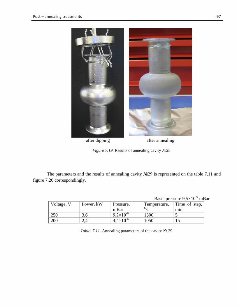
Post – annealing treatments 97
after dipping after annealing
Figure 7.19. Results of annealing cavity 25
The parameters and the results of annealing cavity 29 is represented on the table 7.11 and
figure 7.20 correspondingly.
Basic pressure 9,5×10⁻⁹
mBar
Voltage, V Power, kW Pressure,
mBar
Temperature, OC
Time of step,
min
250 3,6 9,2×10⁻⁶
1300 5
200 2,4 4,4×10⁻⁶
1050 15
Table 7.11. Annealing parameters of the cavity 29

Post – annealing treatments 98
before dipping after dipping after annealing
Figure 7.20. Results of annealing cavity 29
7.3.4 Post annealing treatment
After providing RF – tests of the cavities 22, 25 which showed a high Q – value at low
magnetization, but fast reducing Q – value with increasing the magnetization, we decide to do a
BCP of this cavity in order to reduce roughness of the internal surface. As the solution was chosen
the standard BCP solution. And the durations of etching were 20 and 10 seconds correspondingly.
The result of RF – test of this cavity is also shown in the chapter 7.4.1.
7.3.5 High pressure rinsing
Microparticle contamination has been identified to be the leading cause of field emission.
This stresses the importance of cleanness in all final treatment and assembly procedures. Rinsing
with high pressure ultrapure water (HPR) is the most effective tool to remove microparticles and
therefore reduces field emission [3]. HPR is also effective in reducing field emission which cannot
be processed during an RF-test. The process of HPR of 6 GHz cavity is shown on the figure 7.21.
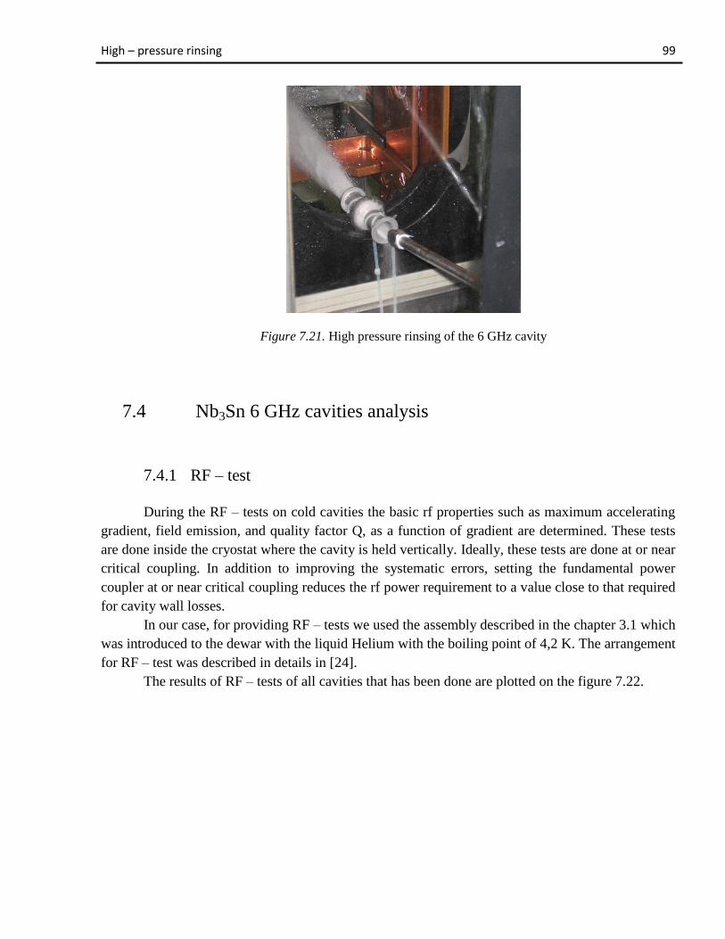
High – pressure rinsing 99
Figure 7.21. High pressure rinsing of the 6 GHz cavity
7.4 Nb3Sn 6 GHz cavities analysis
7.4.1 RF – test
During the RF – tests on cold cavities the basic rf properties such as maximum accelerating
gradient, field emission, and quality factor Q, as a function of gradient are determined. These tests
are done inside the cryostat where the cavity is held vertically. Ideally, these tests are done at or near
critical coupling. In addition to improving the systematic errors, setting the fundamental power
coupler at or near critical coupling reduces the rf power requirement to a value close to that required
for cavity wall losses.
In our case, for providing RF – tests we used the assembly described in the chapter 3.1 which
was introduced to the dewar with the liquid Helium with the boiling point of 4,2 K. The arrangement
for RF – test was described in details in [24].
The results of RF – tests of all cavities that has been done are plotted on the figure 7.22.

RF - test 100
Figure 7.22. The results of RF – tests

Discussion 101
8. Discussion
As it was proved during the previous couple years of research, the “classical” liquid Tin
diffusion technique with use of so called “double furnace process” with resistive furnace annealing
doesn’t shows the satisfactory results on both: the samples and the cavities. The big problem, that
we dialed with, using this technique was the presence of the residual drops of Tin on the surface of
the sample. Cavities, produced by this technology shows the Q – value factor one order of
magnitude lower then pure Niobium cavities. Different combinations of time – temperature regimes
of dipping and annealing were tried but the problem has not been solved. In the light of this
misfortune efforts, we decide to investigate the influence of different additional surface treatments.
Among them there were glow discharge of the sample in the Nitrogen atmosphere, anodization of
the surface in the ammonium citrate and chemical etching with use of the mixture of nitric and
fluoric acids in the 1:1 proportion. This experiments were done with use of L – samples, which has
both vertical and horizontal planes, imitating the problem zones of the cavity (flanges and the
horizontal planes of cell-part). But as it was shown above, each of those samples, independently of
the treatment method has a residual droplets after annealing. That is why we start thinking about the
increasing the annealing temperature. But first of all lets go through the reasons which doesn’t allow
us to work at higher temperatures with “standard” annealing. This reasons are:
use of the external furnace, that means a big losses in heat due to the bad thermal
conductivity of the air, which is in between of the furnace and the vacuum chamber;
the list of possible materials for vacuum chamber, heated up to the temperatures higher then
1000OC is not so wide. In our case was produced the Inconel chamber. The Inconel in used
compound has the melting point of 1100OC, so in any case it is impossible to overcome it;
all the operations must be provided in the ultra high vacuum. But the heated to the
temperature over 1000OC Inconel chamber, due to the thermal expansion allows the
diffusion of contaminations (especially hydrogen) through the wall just from the atmosphere!
and finally, the maximum temperature, that could be reached with the resistive furnace is
1200OC, but it is already not so important, because it is limited by the melting point of the
Inconel.
That’s why we decide to use another approach. We directed our efforts to finding another
king of heater, which doesn’t have all these limitations. These heater is the induction one. Let’s
briefly go through the advantages of induction heater:
The first, and the main advantage is the possibility to reach extremely high temperatures over
2000OC without heating the vacuum chamber;
Possibility to use stainless steel as the material for the chamber;
fast heating of the substrate, which exclude the formation of spurious phases like Nb6Sn5 or
NbSn2;
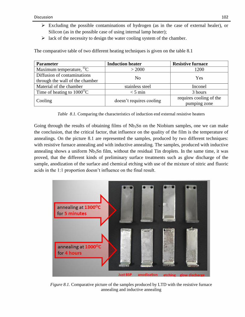
Discussion 102
Excluding the possible contaminations of hydrogen (as in the case of external healer), or
Silicon (as in the possible case of using internal lamp heater);
lack of the necessity to design the water cooling system of the chamber.
The comparative table of two different heating techniques is given on the table 8.1
Parameter Induction heater Resistive furnace
Maximum temperature, OC > 2000 1200
Diffusion of contaminations
through the wall of the chamber No Yes
Material of the chamber stainless steel Inconel
Time of heating to 1000OC < 5 min 3 hours
Cooling doesn’t requires cooling requires cooling of the
pumping zone
Table 8.1. Comparing the characteristics of induction end external resistive heaters
Going through the results of obtaining films of Nb3Sn on the Niobium samples, one we can make
the conclusion, that the critical factor, that influence on the quality of the film is the temperature of
annealings. On the picture 8.1 are represented the samples, produced by two different techniques:
with resistive furnace annealing and with inductive annealing. The samples, produced with inductive
annealing shows a uniform Nb3Sn film, without the residual Tin droplets. In the same time, it was
proved, that the different kinds of preliminary surface treatments such as glow discharge of the
sample, anodization of the surface and chemical etching with use of the mixture of nitric and fluoric
acids in the 1:1 proportion doesn’t influence on the final result.
Figure 8.1. Comparative picture of the samples produced by LTD with the resistive furnace
annealing and inductive annealing

Discussion 103
The results of XRD measurements showed the presence on the surface only the goal
compound, which is Nb3Sn (see pictures 7.9, 7.10).
As for the cavities, the results are also much better. The film of Nb3Sn on the surface of the
resonator is more uniform, without presence of the residual Tin. The highest Q – value has been
obtained on the cavity 5, which was annealed for 9 minutes with the highest temperature of
1485OC. The value of Q in this case is one order of magnitude higher then the Q – value of the
cavities annealed on the resistive furnace, and equals 1,6×10⁻⁷
, that is pretty close to the pure Nb.
Discussion 104
Future developments
The most important thing to do is the improvement of the inductive annealing technology,
keep finding the best possible ratio of time/temperature of dipping – time/temperature of annealing
parameters.
Another important thing to do is the improvement of the induction annealing system such as
designing and installation the water cooling system of the chamber in order to prevent metalising the
window with Tin during the annealing process.
As for the samples our future efforts will be directed to the estimation of the optimal
thickness of the coating, providing the SEM analysis in order to understand the crystal structure of
the films, the XRD measurements for defining the composition.
The future work with the cavities will be dialed with efforts to obtain the maximum
uniformity of the film, and maximum Q – value. The new cryostat has been designed and build, that
will give us a possibility to measure three cavities simultaneously.
List of tables 105
Conclusions
The main purpose of this work was to increase the quality of thermally diffused Nb3Sn
superconductive films over Nb substrates and in particular to avoid the residual droplets of
unreacted Tin on the substrate after annealing that was the problem of last couple of years. In order
to get a good result two different approaches were applied:
improving of existing “double furnace technology” by means of different surface pre-
treatments, and variation of the time/temperature process parameters;
development of the new high – temperature annealing technology.
In the framework of improving the “double furnace technology” we studied the influence of
preliminary surface treatments such as surface glow discharge, anodization and chemical etching.
But it was absolutely proved, that this additional treatments doesn’t influence on the quality of the
film obtained.
Developing the new technology of high temperature annealing we designed and build the
new experimental set up for annealing the 6 GHz cavities by means of induction heater instead of
external resistive furnace. With new system it is possible to reach the temperatures over 1800OC in
less than 5 minutes while the chamber remains relatively cold.
With the new technology it became possible to avoid the residual Tin droplets by means of
increasing the temperature of annealing. Samples that were made with use of inductive annealing
had the uniform coating. The XRD analysis proved that the only one component of the film is
Nb3Sn. But the Tc value of the samples is not yet satisfactory.
The 6 GHz cavities that had been annealed with induction system had much better Nb3Sn
film than the ones made by “double furnace technology”. Unfortunately it still doesn’t have the
desirable uniformity of the film, but also it doesn’t have the residual unreacted Tin. The Q – value of
the cavities annealed has the order of magnitude 10-7
that is close to the Q – value of pure Niobium
cavities.
Also it has been estimated the optimal ratio of time/temperature of dipping –
time/temperature of annealing. For the best cavity produced the dipping parameters were 15 minutes
at 700OC and annealing during 6 minutes at 1800
OC.
However the thermal diffusion technology of obtaining the Nb3Sn films has not yet achieved
its potential performance, but now we have a powerful instrument to advance quickly.

List of tables 106
List of tables
1.1 Comparison of bulk – metal superconductors…………………………………………. 20
1.2 Tc of different B1 compounds………………………………………………………….. 20
6.1 Glow discharge parameters…………………………………………………………….. 54
6.2 Obtained films on the L – samples by LTD with resistive furnace annealing………… 62
6.3 Tumbling parameters for the 6 GHz cavities…………………………………………... 69
6.4 Parameters and results of coating 6 GHz cavities……………………………………… 73
7.1 Parameters of the samples dipping process…………………………………………… 80
7.2 Parameters of the induction oven………………………………………………………. 84
7.3 Annealing parameters of the L-samples 1-2, 2-2, 3-2, 4-2…………………………….. 86
7.4 Annealing parameters of the LL-samples 1-3, 2-3, 3-3, 4-3, 5-3, 6-3…………………. 87
7.5 Results of measuring Tc and ΔTc on the LL – samples………………………………… 90
7.6 Dipping parameters of the cavities 33, 5, 25, 29………………………………… 91
7.7 1st annealing parameters of the cavity 33…………………………………………… 94
7.8 2nd
annealing parameters of the cavity 33………………………………………….. 95
7.9 Annealing parameters of the cavity 5………………………………………………. 96
7.10 Annealing parameters of the cavity 25……………………………………………… 97
7.11 Annealing parameters of the cavity 29……………………………………………… 97
8.1 Comparing the characteristics of induction end external resistive heaters…………… 102

List of figures 107
List of figures
0.1 A bulk Niobium tesla – type 9 cells superconductive cavity…………………………... 13
0.2 Schematic of a generic speed-of-light cavity. The electric field is strongest near the
symmetric axis, while the magnetic field is concentrated in the equator region………. 14
1.1 Crystal structure of B1 materials………………………………………………………. 21
2.1 Crystal structure of A-15 materials…………………………………………………….. 22
1.2 Critical temperatures of binary A15 compounds known to be superconducting………. 24
1.3 The niobium germanium phase diagram……………………………………………….. 25
1.4 Niobium Gallium phase diagram………………………………………………………. 26
1.5 (a): The A15 phase field in the Nb-Ga system; (b): the variation of critical
temperature Tc with composition along the Ga-rich phase boundary…………………. 26
1.6 Portion of the niobium aluminum phase diagram……………………………………… 27
1.7 V3Si: RRR values versus silicon content………………………………………………. 28
1.8 V3Ga: Vanadium gallium phase diagram………………………………………………. 29
3.0 On the right the scrap, of a large Nb – cavity, from which is possible to obtain 4
6GHz cavities (on the left) without any welding by spinning technology……………... 30
3.1 Stand for providing rf-test of 6 GHz cavities…………………………………………... 31
3.2 The 6 GHz cavity geometry……………………………………………………………. 31
3.3 Producing of the 1,5 GHz cavity by spinning technology……………………………... 32
3.4 6 GHz Nb cavities, produced by spinning technology…………………………………. 33
4.0 Niobium – Tin phase diagram………………………………………………………….. 34
4.1 Niobium – Tin crystal structure………………………………………………………... 35
4.2 Tc as a function of the Sn content……………………………………………………… 36
5.1 Schematic illustration of the alignment of magnetic moments for different types of
materials……………………………………………………………………………....... 41
5.2 Hysteresis curves. A virgin hysteresis curve (a) and a full hysteresis curve (b)………. 43
5.3 Parallel resonant tank circuit. 1, 2 – different values of current……………………….. 45
5.4 The L – matching network……………………………………………………………... 46
5.5 The LCLR work coil…………………………………………………………………… 47
5.6 Half bridge induction heater using LCLR – work coil………………………………… 48
5.7 Full bridge induction heater using LCLR – work coil…………………………………. 49
6.0 Shape of L-sample (a), and number of the sample (b)…………………………………. 52
6.1 L-samples with and without BCP……………………………………………………… 52
6.2 The glow discharge chamber (a) and the feedthrough with L-sample connected…….. 53
6.3 Relationship between the current, supplied to the coil and inducted magnetic field….. 54
6.4 Glow discharge process………………………………………………………………... 55
6.5 Anodization laboratory stand (a) and the L-sample after anodization treatment (b)… 56
6.6 Chemical etching process…………………………………………………………….... 57

List of figures 108
6.7 Experimental apparatus for dipping……………………………………………………. 58
6.8 Al2O3 crucible with Tin inside (a), and samples (cavity) support (b)………………….. 58
6.9 Controlling unit………………………………………………………………………… 59
6.10 Photograph of the liquid tin diffusion experimental stand…………………………….. 60
6.11 The way to fix the samples on the support…………………………………………….. 60
6.12 L – samples after dipping………………………………………………………………. 61
6.13 L – samples covered with Nb3Sn with different surface treatments techniques………. 63
6.14 L – samples covered with Nb3Sn with different surface treatments techniques……….. 64
6.15 Zr oxide balls and SiC pieces for tumbling…………………………………………….. 65
6.16 6 GHz cavity and the plastic flange with o-ring……………………………………….. 66
6.17 Filled with the media cavities fixed in a tumbling support……………………………. 66
6.18 Tumbler drawing……………………………………………………………………….. 67
6.19 Photograph or the tumbler……………………………………………………………… 67
6.20 Mini-camera for taking pictures of the internal surface of the cavity and the results of
6GHz cavity tumbling (cell-part)………………………………………………………. 69
6.21 Stand for pulsed BSP of 6 GHz cavity…………………………………………………. 70
6.22 Internal surface of the cavity-cell part before (a) and after (b) BCP…………………... 70
6.23 The way to fix the cavity on the support………………………………………………. 71
6.24 Zones of the highest concentration of unreacted Tin on the 6 GHz cavity surface (Tin
is marked by the red color)…………………………………………………………….. 72
6.25 External surface of the cavity 1 after first annealing. Tin accumulation on the upper
part of the cell (a), clear lower part of the cell (b) and the layer of Tin on the lower
flange (c)……………………………………………………………………………….. 73
6.26 External surface of the cavity 1 after first annealing. Tin accumulation on the upper
part of the cell (a), upper flange and the support (b) and the layer of Tin on the lower
flange (c), (d)…………………………………………………………………………… 74
6.27 External surface of the cavity 2 after annealing. Tin accumulation on the upper part
of the cell (a), and the lower flange (b)………………………………………………… 74
6.28 External surface of the cavity 3 after annealing. Tin accumulation on the upper part
of the cell (a), lower part of the cell is clear (b), and the lower flange (b) is covered
with the layer of Tin……………………………………………………………………. 75
6.29 Internal surface of the cavity 1 after first annealing. Accumulation of residual Tin
on the different parts of the cavity……………………………………………………... 76
6.30 Results of measuring the Qvalue of the cavity with Nb3Sn film and residual Tin
droplets in comparison with pure Niobium cavity, which was treated just
mechanically and BCP…………………………………………………………………. 77
7.2 Film obtained as the result of dipping on LL – samples……………………………….. 80
7.3 Inductive annealing stand………………………………………………………………. 81
7.4 Lower flange with work coil (a) and the ZrO2 balls in the lower flange capacity (b)…. 82
7.5 Process of L-samples annealing………………………………………………………... 84
7.6 Pyrometer IRtec P-2000………………………………………………………………... 84
7.7 The photograph of the L-samples 1-2, 2-2, 3-2, 4-2 after annealing in the induction 85

List of figures 109
oven……………………………………………………………………………………..
7.8 The photograph of LL-samples 1-3, 2-3, 3-3, 4-3, 5-3, 6-3 after annealing in the
induction oven…………………………………………………………………………. 86
7.9 The bulk scan XRD spectra of the sample, produced by LTD with annealing in the
induction oven………………………………………………………………………….. 87
7.10 The thin film scan XRD spectra of the sample, produced by LTD with annealing in
the induction oven……………………………………………………………………… 88
7.11 Two coil arrangement of the inductive Tc set up………………………………………. 89
7.12 Cavity after dipping step. Cavity 5 (a) produced without post heating, and cavity
25 (b) produced with post heating……………………………………………………… 91
7.13 Cavity fixed on the support for annealing……………………………………………… 92
7.14 Relation between the output inductor voltage and the temperature of the cavity……… 92
7.15 Cavity annealing process………………………………………………………………. 93
7.16 Results of annealing cavity 33………………………………………………………. 94
7.17 Tin – plasma inside the vacuum chamber during the annealing of the cavity………… 95
7.18 Results of annealing cavity 5………………………………………………………... 96
7.19 Results of annealing cavity 25………………………………………………………. 97
7.20 Results of annealing cavity 29………………………………………………………. 98
7.21 High pressure rinsing of the 6 GHz cavity…………………………………………….. 99
7.22 The results of RF – tests……………………………………………………………….. 100
8.1 Comparative picture of the samples produced by LTD with the resistive furnace
annealing and inductive annealing……………………………………………………... 102

Bibliography 110
Bibliography
[1] Michael Tinkham. Introduction to Superconductivity, 2nd edition (1996). McGraw-Hill
[2] J. Bardeen, L. Cooper, J. R. Schrieffer, Theory of superconductivity, Physical Review 108 (1957)
1175.
[3] H. Padamsee, J. Knoblock, T. Hays, RF Superconductivity for Accelerators, Wiley and Sons, New
York, 1998
[4] J. Jackson, Classical Electrodynamics, Wiley, New York, 2nd edition, 1975.
[5] K. Halbach, R. Holsinger, Particle Accelerators 7 (1976) 213 – 222.
[6] B. Bonin, Commissariat à l’Energie Atomique, DSM/DAPNIA, France « Materials for
superconducting cavities »
[7] R. Vaglio, Alternative superconducting materials for rf cavity applications., in: Proceedings
of the 8th Workshop on RF Superconductivity, Abano Terme, Padova, Italy,1997.
[8] S.V.Vonsovsky, Yu.A.Izyumov, E.Z.Kumaev, "Superconductivity of transition metals",
Springer-Verlag (1982)
[9] V. Palmieri Istituto Nazionale di Fisica Nucleare, Laboratori Nazionali di Legnaro, Legnaro
(Padua), ITALY «New Materials for Superconducting Radiofrequency Cavities» Proceedings
for the 10th Workshop on RF Superconductivity, 2001, Tsukuba, Japan
[10] G.F.Hardy and J.K. Hulm, Phys. Rev. 87, 884 (1953); 93, 1004 (1954)
[11] B.T. Matthias, T. Geballe, S. Geller, F. Corenzwit, Phys. Rev. 95, 1435 (1954)
[12] S.V.Vonsovsky, Yu.A.Izyumov, E.Z.Kumaev,"Superconductivity of transition metals, their
alloys and compounds", Springer-Verlag (1982)
[13] R. Blaugher, R. Hein, R. Cox, J.E. and Waterstrat, J. Low Temp. Phys. 1 (1969) 531.
[14] E. Savitskii, V. Baron, Y. Efimov, M. Bychkova, L. Myzenkova, Superconducting Materials,
Plenum Press, New York, 1973.
[15] J. Jorda, R. Flukiger, J. Muller, J. Less-Common Met. 55 (1977) 249.
[16] S. Moehlecke, PhD Thesis, Universidad Estudial de Campinas, Brazil, 1977.
[17] H. Maeda, K. Inoue, T. Kiyoshi, T. Asano, Y. Sakai, T. Takeuchi, K.Etoh, K. Aoki and G.
Kido, Physica B 216, 141 (1996)
Bibliography 111
[18] A. Godeke, International SRF Thin Films Workshop 2006, INFN-LNL,
http://master.lnl.infn.it/thinfilms/ (Lawrence Berkeley National Laboratory. Paper LBNL-
62140)
[19] J. Yasatis, R. Rose, IEEE Trans. Magn. 11 (1975) 434.
[20] Proceedings de “14th International workshop on RF Superconductivity” (SRF 2009), p.149;
web site: http://accelconf.web.cern.ch/AccelConf/srf2009/papers/tuobau06.pdf
[21] Proceedings de “14th International workshop on RF Superconductivity” (SRF 2009), p.155;
web site:http://accelconf.web.cern.ch/AccelConf/srf2009/papers/tuobau07.pdf
[22] V. Palmieri, .Spinning of TESLA-Type Cavities: Status of Art., Proc. of the 9th Workshop on
RF superconductivity, Santa Fe, USA, Nov. 1999, pp 532-537.
[23] C. Pira “Titaniocromia tramite ossidazione anodica”. Bachelor thesis, academic year 2003-
2004. Supervisor prof. V. Palmieri.
[24] S.M. Deambrosis “A method to test A-15 intermetallic compounds rf properties”. PhD thesis,
academic year 2007-2008. Supervisor prof. V. Palmieri.
[25] S.M. Deambrosis, V. Rampazzo, A.A. Rossi, V. Rupp, R.G. Sharma, S. Stark, F. Stivanello,
and V. Palmieri “A-15 superconductors by thermal diffusion in 6 GHz cavities” Proceedings
of SRF2009, Berlin, Germany
[26] M. Straumanis, S. Zyszczynsk, J. Appl. Cryst. 3 (1970) 1
[27] H. Devantay, J. Jorda, J. Decorux, M. and Muller, R. Flukiger, J. Mat. Sci. 16 (1981)
2145
[28] D. Dew-Hughes, Cryogenics 15 (1975) 475.
[29] R. Flukiger, H. Kupfer, J. Jorda, J. Muller, IEEE Trans. on Magn. MAG-23 (1980)
980.
[30] M. Beasley, Adv. Cryog. Eng. 28 (1982) 345.
[31] Julius Adams Stratton. Electromagnetic theory. IEEE Press, Piscataway, NJ, 2007.
[32] Mattew N.O. Sadiku. Elements of Electromagnetics, volume 3. Oxford University Press, Inc.,
2001.
[33] Web site dedicated to induction heating systems http://www.richieburnett.co.uk/indheat.html