the electronic watch and low-power circuits · the electronic watch and low-power circuits ... led...
TRANSCRIPT

Solid-State Circuits Society http://www.ieee.org/portal/site/sscs/menuitem.82c662ad8f3c2e3deef9cf...
1 of 19 8/16/2008 9:25 AM
The Electronic Watch and Low-Power CircuitsEric A. Vittoz, IEEE Life Fellow member, [email protected]
New Research LaboratoryThis story starts in 1962 with the foundation of CEH (Centre Electronique Horloger or “Watchmakers Electronic Center”). Thebipolar junction transistor (BJT) was 14 years old and had already replaced the vacuum tube in most electronic systems. A fewyears had passed since the invention of the integrated circuit, followed by that of the planar process by Swiss born physicist JeanHoerni.
The Swiss watch industry was flourishing, exporting about 45 million watches per year for a total value of 1.4 billion Swiss francs.But it was undergoing a deep structural mutation from its traditional organisation based on corporatism. The whole watch industrywas of a fully mechanical nature and most of the technical managers had been educated as traditional watchmakers. However,for several years, a very few visionary managers had been watching the recent development taking place on the other side of theAtlantic Ocean, in this strange new domain for them called solid-state electronics.
Led by Gerard Bauer, the dynamic director of the Federation of the Swiss Watch Industry (FH), a research group representingthe major Swiss manufacturers was created, to evaluate if and how this new electronics could once be applicable in some way tothe wristwatch itself. Through the long existing LSRH (“Swiss Laboratory for Watch Research”, founded in the 40’s for research inall aspects of the mechanical watch), they entrusted the Swiss Technical Universities with some limited contracts to evaluatethese possibilities. They received rather negative conclusions, but however decided that a new joint center would be created tosearch for possible new watch systems based on electronics. After receiving enthusiastic support from Sydney de Coulon, thegeneral Director of Ebauches SA, the powerful producer of all Swiss watch components, they hired Roger Wellinger as technicalDirector to lead the project. A Swiss electrical engineer, Roger had spent 15 years in the USA, first as an Associate Professor ofEE at Illinois State University in Urbana, then with General Electric in Schenectady.
In 1962 CEH, the new joint research laboratory, was founded in Neuchâtel by several organisations representing most of theSwiss watch industry, with a tentative global budget of 5 million Swiss Francs, to be released year after year. The generalmission of CEH was to develop new time-keeping devices. This goal was soon refined into that of developing an electronicwristwatch, with at least one advantage with respect to existing watches. No need to say that, at that time, few people couldimagine that one of the main advantages would be a much lower production cost for a better precision.
There was no real market pull: most people were happy with the precision of their automatic mechanical watch. Some electricalwatches had recently appeared on the market, replacing the mechanical drive by an electromagnetic actuator driven from a smallmercury battery through a mechanical switch. A French patent was proposing to replace the switch by a transistor (which wasrealized a few years later). However, this modest change did not bring much advantage, and those approaches were soonabandoned.
The only really new wristwatch was the Accutron that had been developed for Bulova by Swiss engineer Max Hetzel. Based on ametallic tuning fork oscillating at 360Hz and activated by a single transistor, this revolutionary watch had been commercialized in1960. It was, however, still essentially mechanical, with a complex wheel-ratchet system driving the set of gears, and at afrequency too low to avoid being affected by gravity.
The electronic quartz clock had already been invented by Warren Marrisson in 1928, and transistorized quartz marinechronometers were just available. Their volume was 1.5dm3, and their power consumption larger than 100mW. Hence a quartzwristwatch did not have to be invented: it already existed as a system. The “only” challenge was to reduce its volume to less than3cm3, and to lower its power consumption by 4 orders of magnitude, down to less than 10μW. This was the maximum acceptablepower consumption to ensure more than one year of life for the 1.35V mercury button cell compatible with the wristwatch volume.
This new lab was initially lodged just under the roof of the LSRH building in Neuchâtel (Fig. 1). In May 1962, I was the very firstelectrical engineer hired at CEH by Roger Wellinger.

Solid-State Circuits Society http://www.ieee.org/portal/site/sscs/menuitem.82c662ad8f3c2e3deef9cf...
2 of 19 8/16/2008 9:25 AM
Fig. 1: LSRH building in Neuchâtel, Switzerland. During its firstyear, CEH was lodged just under the roof of the main buildingat the left. It then moved to this wing, where the process line was installed.
A Passion for ElectricityI was born in 1938 in Lausanne. As far as I can remember, I have always been fascinated by electricity. My grandfather was anelectrical engineer working for a local power company. His cellar was a cave of treasures, full of various discarded electricitycounters. Back home, I used to take them apart, collecting the various parts. Most interesting was the sub-millimeter isolatedcopper wire of the coils. When I was about six years old, my first applications for it were 220V in-house electrical networks. Toconnect the meccano-made switches and light bulbs, I just had to scratch the isolation at the wire end with my teeth, bend it, andput it into the power plug. I learned the hard way the meaning of closing an electrical loop when I put my hands both sides of theswitch! Nobody seemed to be really worried by the number of shocks I received during this early learning period. However, myfather (also an engineer, but in civil engineering) finally decided that I should go to low voltage and he mounted an old radiotransformer in a wooden box with just the 6.3V for filament heating available from outside.
My education was in classical literature, with the threat of “descending” to scientific if my results were not good enough (so wasthe hierarchy of matters at that time!). But I lost no opportunity to communicate my passion to my classmates. When theirpresentations to the class were about poets and musicians, mine were about electronic recording and electrical transformers(with a demo based on a self-made high-voltage transformer driven by a 4.5V battery chopped by an electric doorbell!).Applications of Ohm’s law were the subject of a summer technical contest for which I built a series of demonstrators.
My interest soon concentrated on electronics, which at that time was almost synonymous to radio. At 14, I had built from scratchmy first short-wave receiver, winding the thousands of turns of the 2x350V high voltage and manually sawing and bending thealuminium plates to mount the components. I passed my ham radio license at 18 and came “on the air” with a self-madetransmitter, with an output power of 10W delivered by a Telefunken RL12P35 power tube (Fig. 2 shows a later version of mystation). This was my first contact with the USA and an excellent opportunity to start practicing my school English. I still feel theexcitement of waiting for an “opening” of the 10 meters band to contact American or Australian stations as if they were next door!With the Internet, the excitement of distant communication is lost nowadays, but at that time it was achieved with nothing morethan my homemade rig.

Solid-State Circuits Society http://www.ieee.org/portal/site/sscs/menuitem.82c662ad8f3c2e3deef9cf...
3 of 19 8/16/2008 9:25 AM
Fig. 2: At my homemade ham radio station HB9VZ in 1959.
I received my technical education from the “Ecole Polytechnique de l’Université de Lausanne” (EPUL, that later became EPFL,the Swiss Federal Institute of Technology), where the only professor of electronics was Roger Dessoulavy. I watched him as agod until I could finally attend his courses, during the 4th and last year. Most of the course was based on the vacuum tube, withjust two sessions devoted to the transistor. Upon my request, my diploma project was part of a transistorized A/D converter. Ithen spent one year as a research assistant, working in the ancient gardener’s house of EPUL and helping to speed up thisconverter to audio frequencies. That’s where Wellinger found me and asked me to join his new team. We moved to Neuchâtelwith my young wife Monique. She was going to provide me with an essential support all along my career.
Initial Research PeriodMy very first task was to demonstrate that a quartz clock could be operated with the power consumption compatible with awristwatch. I delivered a demonstrator (Fig. 3) that combined an oscillator circuit with a 10kHz commercial quartz, followed by 4divide-by-ten stages, in order to reduce the frequency down to 1Hz. These dividers were synchronized astable multivibratorsusing 2N1711 planar bipolar transistors produced by SGS that exhibited a large current gain much below the microampere level.All of the electronics was consuming less than 10μA at 1.5V. But the display was a commercially available electric clock using astepping motor and consuming more than 1mW. With this simple demonstrator on the table, Roger Wellinger had his 1.8 millionfranc budget for 1963 accepted by the board of directors. The real work could start, but experienced engineers were needed.

Solid-State Circuits Society http://www.ieee.org/portal/site/sscs/menuitem.82c662ad8f3c2e3deef9cf...
4 of 19 8/16/2008 9:25 AM
Fig. 3: Microwatt clock demonstrator.
Roger was a very enthusiastic and visionary manager. Using all possible means, he was able to convince a bunch of talentedSwiss engineers emigrated in the USA to abandon their interesting and promising jobs to come back to Switzerland and bringtheir experience to CEH. Among them, Max Forrer left General Electric in Palo Alto to lead the circuit and system section (hebecame my direct boss for the next 27 years!), and Kurt Hübner came to lead the microelectronic section with his 5-yearexperience at the Shockley Semiconductor Lab. The real work then started on four parallel paths.
Most essential was the building-up of an in-house IC facility, and the development of a process adapted to low voltage and verylow power. Although the first functional MOS transistors had already been published, it was decided to start concentrating on themore traditional bipolar process. A fully operational facility, including a mask shop, was installed in the west wing of the LSRHbuilding (Fig. 1).
The second activity was the search for an adequate time base. The goal was to obtain a precision better than 10ppm(corresponding roughly to 1 second per day) at a frequency lower than 10kHz, to limit the power needed for frequency division.The size of existing quartz resonators at this frequency was much too large, and experts in the field pretended that there was noway to reduce it without drastically reducing the quality factor. Hence we first searched for various types of metallic resonatorscombined with piezoelectric or electromagnetic transducers. We even evaluated a statistical time base using alpha particlesemitted by a radioactive source.
But none of these approaches ended successfully. It is the merit of Armin Frei, another Swiss engineer repatriated from the USA,to have attacked and solved the problem of reducing the size of a sub-10kHz quartz resonator. Against all odds and predictions,he was finally able to mount a miniaturized 8192Hz quartz oscillating in flexural mode in the vacuum of a small metallic package(Fig. 4).

Solid-State Circuits Society http://www.ieee.org/portal/site/sscs/menuitem.82c662ad8f3c2e3deef9cf...
5 of 19 8/16/2008 9:25 AM
Fig. 4: First prototype of 8192Hz small size quartz resonatordeveloped at CEH.
The third activity was a search for an adequate display system. The LCD did not exist yet and the LED had just beendemonstrated. It was decided to rely on electromechanical solutions, by taking advantage of the matchmakers’ skills inmicromechanics. Various schemes were evaluated, using electromagnetic and piezoelectric actuators. Two electromagneticsolutions were finally retained for the first prototypes.
The fourth activity was in electronics, essentially evaluating different frequency divisions. I was mostly involved in thisdevelopment; hence, I can describe it with more details.
Planar technology was very novel and only able to combine just a few components per chip. The rate at which this number couldbe increased was uncertain. No low-power process was available yet, and we did not discard the possibility to build the firstwatch by using discrete components. Therefore, our first aim was to minimize the number of components, and we started bylooking into all kinds of analog division techniques.
One possibility was to use synchronized relaxation oscillators (Fig 5a). I tried various schemes, including one based on the tunneldiode (that was considered a very promising device at that time). Another scheme consisted in the step-by-step accumulation ofsome quantity until a threshold would be reached (Fig. 5b). I first tried to accumulate magnetic flux in a tiny toroidal magnet (ofthe kind used for computer memories at that time), but the energy per cycle was too high. A better solution was to accumulate acharge in a capacitor, in a kind of switched capacitor integrator, combined with a discharge circuit made of complementary BJT’s.A hybrid version of a single divide-by-eight stage mounted in a TO5 package was presented at the 1964 International Congressof Chronometry (where CEH was asked to be present, although we were normally supposed to keep our results secret!).
Fig. 5: Analog frequency division techniques; (a) Relaxation oscillatorsynchronized by pulses; (b) Step by step accumulation. Fig. 6: Principle of phaselock loop frequency division.
It is during this period that I made my first visit to the USA, to attend the ISSCC’64 that was still held in Philadelphia. During anevening panel on “Minimum power solid-state devices and circuits”, I was asked by a friend of Wellinger to say a few words aboutour work for an electronic watch. As I can remember, this idea was considered foolish, if not impossible! This trip was also afantastic opportunity to visit a number of companies and universities and to meet personalities whose famous names wereassociated with the incipient semiconductor technology.
Analog solutions were indeed limiting the number of components, but the maximum possible dividing ratio was limited by theprecision of these components. No more than a factor ten per stage could be expected, even less with the intended integrated

Solid-State Circuits Society http://www.ieee.org/portal/site/sscs/menuitem.82c662ad8f3c2e3deef9cf...
6 of 19 8/16/2008 9:25 AM
versions. So I looked for an analog solution that could provide a very large divider ratio even with low-precision components. Thiswas based on a phaselock loop as illustrated by Fig. 6.
The loop was made of a low frequency VCO (astable multivibrator) followed by a pulse shaper, the output p of which sampled the high frequency input. The result was held by a second order filter that produced the voltage vc controlling the VCO frequency. The phase of the VCO could be locked to that of the input signal for any frequency ratio N = fin/fout that was keeping fout insidethe hold range of the loop. The divider ratio was controlled by the initial condition imposed to the loop (and stored in its filter). Thehold range could be made large enough to compensate for even a large error in the natural frequency of the VCO. The maximumpossible ratio N was limited by the jitter of the VCO. Indeed, this jitter was producing a phase noise proportional to N, thus a probability of unlocking increasing with N.
A breadboard implementation of this divider (which became the subject of my Ph.D. thesis) is shown in Fig. 7. Without theoscillator, this divider contained only 3 bipolar transistors, 4 discrete MOS transistors fabricated at CEH and a few resistors andcapacitors. A frequency ratio as high as 1000 could be obtained by means of just a few low-precision components. Consuming afew microamperes at 1.35V, it stayed in lock during the years needed to write my dissertation. This project was a lot of fun. It wasan opportunity to learn about nonlinear and discrete-time systems, and it made me love the subject of PLL. But the reliability wasdefinitely not sufficient (risk of loosing the ratio) to consider a mass production of watches based on this approach. Fortunately, inthe meantime, our in-house process developments were sufficiently advanced to consider using a cascade of integrated binarydividers instead.
Fig. 7: Experimental phaselock loop frequency divider. It includes a 8kHzoscillator based on an early quartz prototype.
The first binary divider that we developed in 1966 (Fig. 8) was a modified version of a circuit found in the literature, itself atransistor implementation of the T-Flip-Flop used with vacuum tubes. The idea of current mirrors had not been proposed yet, andneither was the implementation of lateral pnp’s (although both ideas seem so obvious a posteriori, like so many great ideas!).Hence, high-value resistors were the only available way to reduce the power. They were implemented by using the base layer,pinched between emitter E and collector C. Their maximum frequency of operation was thus limited by a large distributedcapacitor and could be maximized by letting the E and C layers unconnected (floating). Implemented with our 10 micron bipolarprocess, this divider could operate up to 5kHz for a current drain of 1μA.
Fig. 8: First binary frequency divider. Fig. 9: First prototypes of the quartzwristwatch developed by CEH.
Circuit simulators did not exist yet, so circuits had to be verified on a breadboard before integration. All parasitic capacitors wereextracted manually from the layout, but these were of course smaller than those associated with the breadboard itself. Tocircumvent this problem, the value of all extracted capacitors was multiplied by a large factor (typically 1000), whereas thefrequency was reduced by the same factor. The dynamic behaviour of the integrated version could then be predicted with goodprecision. We used this simulation technique during many subsequent years, until circuit simulators and transistor models at verylow current were finally available.
It is this integrated frequency divider that was used in the first prototypes of the electronic watch.

Solid-State Circuits Society http://www.ieee.org/portal/site/sscs/menuitem.82c662ad8f3c2e3deef9cf...
7 of 19 8/16/2008 9:25 AM
The First Quartz Wristwatch [1]The efforts of the various groups at CEH came to convergence with the realization of two different prototypes of the quartzwristwatch (Fig. 9). Both used the 8192Hz quartz cantilever developed by Armin Frei, driven by a symmetrical negativeresistance circuit. Prototype Beta 1 needed 13 stages of binary division followed by some logic to drive the moving coil of a 1Hzstepping motor. In order to reduce the power consumption, prototype Beta 2 had only 5 stages of division. The 256Hz output wasdriving an electromagnetic resonant motor, with a ratchet driving the train of wheels. In 1967, ten of these prototypes werepresented at the Neuchâtel Chronometry Observatory where they pulverized all previous results. They were then disclosed to ourunsuspecting shareholders in a memorable technical seminar.
The industrial production was organized by CEH in collaboration with several interested watch companies. It was decided to startfrom the Beta 2 prototype to ensure a battery life longer than one year. All the circuitry was integrated on a single chip, under theresponsibility of Raymond Guye. This very first large scale integration circuit for a watch (Fig. 10) combined 110 components(NPN transistors, high-value diffused resistors and junction capacitors) in an area of 8.7mm2, and was consuming 12μA at 1.3V.Several other modifications of the watch prototype were introduced to realize the industrial version (Fig. 11) that was named Beta21. An electronic module was supporting the quartz (not visible in the picture), the plastic encapsulated chip, and an adjustabletrimmer capacitor for fine frequency adjustment. The latter became the source of many problems and would have to beeliminated in the future. The components were fabricated by several Swiss companies, but the circuit was produced by CEH inthe IC facilities of its microelectronic division. A total of about 6000 units were delivered, and sold under different Swiss tradenames.
Fig. 10: First LSI circuit developed fora wristwatch.
Fig. 11: Beta 21, module of the firstcommercial watch developed at CEH.
I personally made very few direct contributions to the development of this first industrial product. Indeed, since 1967, and inparallel with the drafting of my Ph.D. dissertation, I was involved in the very early development of low-voltage CMOS circuits.
Pioneering Low-Voltage CMOS CircuitsWhile most CEH collaborators were busy working on the first watch prototypes, Fritz Leuenberger was developing a low-voltageCMOS process. Fritz had joined CEH after working in the semiconductor department of General Electric in Syracuse. Followingthe key paper of Wanlass and Sah at ISSCC’63 [2], and strongly supported by Max Forrer, he started developing low-thresholdP-channel devices (a few of them were used in my experimental PLL frequency divider) before working on a low-voltage CMOSprocess. In 1968, he had assembled a perfectly workable process [3]. The n-well was obtained by chemically etching the p-typesilicon substrate and epitaxially refilling it with n-type material. The surface was then smoothed by mechanical polishing. Amolybdenum-gold sandwich was used for the gates (and interconnections) to obtain a low threshold voltage for both types oftransistors.
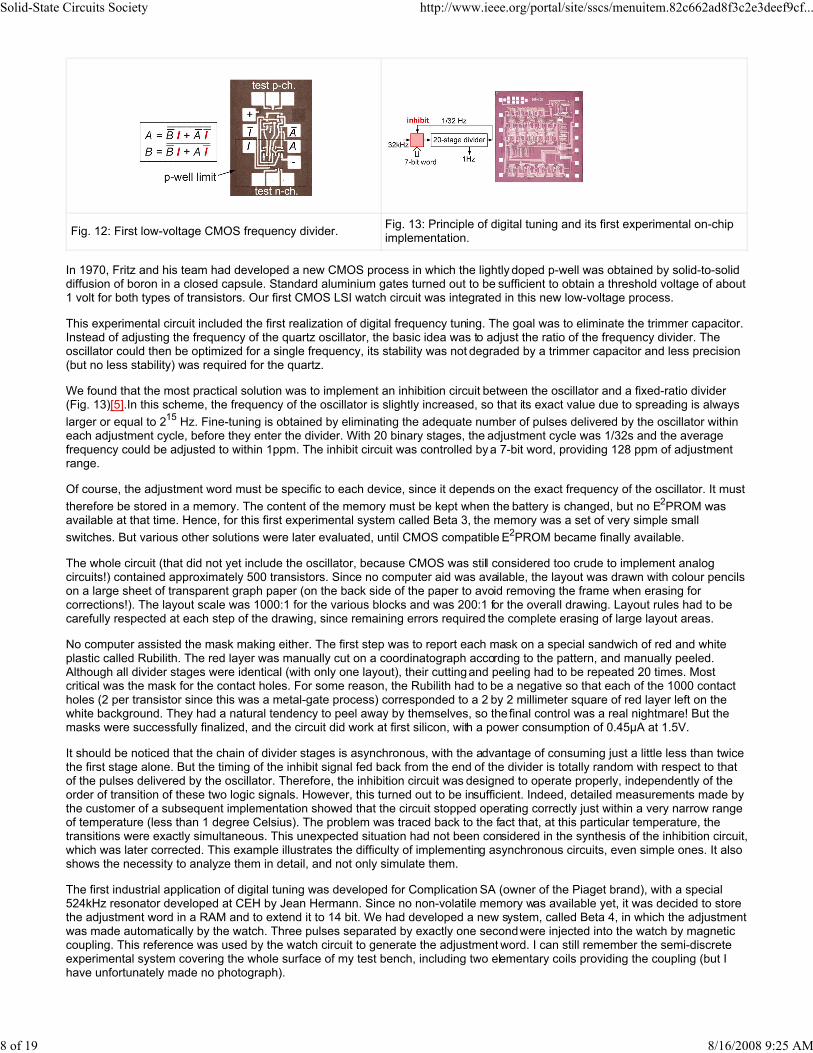
I was asked to design a frequency divider in this new process. A circuit based on transmission gates had been presented atISSCC’67 [4], but its topology was not suited to group P and N channel devices in two distinct areas. Instead, I carried out adirect Huffman synthesis of the divide-by-two function. The resulting logic equations were implemented by means of two 2-levelgates and two inverters (Fig. 12), requiring a total of 16 transistors (after merging some transistors). I drew the layout, and Fritzsuccessfully fabricated the circuit. We measured a current consumption of 10nA/kHz at 1.35V, about 20 times less than thebipolar dividers used in Beta 21. Since the maximum frequency at this low voltage was still about 200kHz, it became possible toincrease the frequency of the oscillator and thereby reduce the size of the quartz resonator. This frequency was later fixed at32kHz and is still used nowadays in most electronic watches.
Solid-State Circuits Society http://www.ieee.org/portal/site/sscs/menuitem.82c662ad8f3c2e3deef9cf...
8 of 19 8/16/2008 9:25 AM
Fig. 12: First low-voltage CMOS frequency divider. Fig. 13: Principle of digital tuning and its first experimental on-chipimplementation.
In 1970, Fritz and his team had developed a new CMOS process in which the lightly doped p-well was obtained by solid-to-soliddiffusion of boron in a closed capsule. Standard aluminium gates turned out to be sufficient to obtain a threshold voltage of about1 volt for both types of transistors. Our first CMOS LSI watch circuit was integrated in this new low-voltage process.
This experimental circuit included the first realization of digital frequency tuning. The goal was to eliminate the trimmer capacitor.Instead of adjusting the frequency of the quartz oscillator, the basic idea was to adjust the ratio of the frequency divider. Theoscillator could then be optimized for a single frequency, its stability was not degraded by a trimmer capacitor and less precision(but no less stability) was required for the quartz.
We found that the most practical solution was to implement an inhibition circuit between the oscillator and a fixed-ratio divider(Fig. 13)[5].In this scheme, the frequency of the oscillator is slightly increased, so that its exact value due to spreading is alwayslarger or equal to 215 Hz. Fine-tuning is obtained by eliminating the adequate number of pulses delivered by the oscillator withineach adjustment cycle, before they enter the divider. With 20 binary stages, the adjustment cycle was 1/32s and the averagefrequency could be adjusted to within 1ppm. The inhibit circuit was controlled by a 7-bit word, providing 128 ppm of adjustmentrange.
Of course, the adjustment word must be specific to each device, since it depends on the exact frequency of the oscillator. It musttherefore be stored in a memory. The content of the memory must be kept when the battery is changed, but no E2PROM was available at that time. Hence, for this first experimental system called Beta 3, the memory was a set of very simple smallswitches. But various other solutions were later evaluated, until CMOS compatible E2PROM became finally available.
The whole circuit (that did not yet include the oscillator, because CMOS was still considered too crude to implement analogcircuits!) contained approximately 500 transistors. Since no computer aid was available, the layout was drawn with colour pencilson a large sheet of transparent graph paper (on the back side of the paper to avoid removing the frame when erasing forcorrections!). The layout scale was 1000:1 for the various blocks and was 200:1 for the overall drawing. Layout rules had to becarefully respected at each step of the drawing, since remaining errors required the complete erasing of large layout areas.
No computer assisted the mask making either. The first step was to report each mask on a special sandwich of red and whiteplastic called Rubilith. The red layer was manually cut on a coordinatograph according to the pattern, and manually peeled.Although all divider stages were identical (with only one layout), their cutting and peeling had to be repeated 20 times. Mostcritical was the mask for the contact holes. For some reason, the Rubilith had to be a negative so that each of the 1000 contactholes (2 per transistor since this was a metal-gate process) corresponded to a 2 by 2 millimeter square of red layer left on thewhite background. They had a natural tendency to peel away by themselves, so the final control was a real nightmare! But themasks were successfully finalized, and the circuit did work at first silicon, with a power consumption of 0.45μA at 1.5V.
It should be noticed that the chain of divider stages is asynchronous, with the advantage of consuming just a little less than twicethe first stage alone. But the timing of the inhibit signal fed back from the end of the divider is totally random with respect to thatof the pulses delivered by the oscillator. Therefore, the inhibition circuit was designed to operate properly, independently of theorder of transition of these two logic signals. However, this turned out to be insufficient. Indeed, detailed measurements made bythe customer of a subsequent implementation showed that the circuit stopped operating correctly just within a very narrow rangeof temperature (less than 1 degree Celsius). The problem was traced back to the fact that, at this particular temperature, thetransitions were exactly simultaneous. This unexpected situation had not been considered in the synthesis of the inhibition circuit,which was later corrected. This example illustrates the difficulty of implementing asynchronous circuits, even simple ones. It alsoshows the necessity to analyze them in detail, and not only simulate them.
The first industrial application of digital tuning was developed for Complication SA (owner of the Piaget brand), with a special524kHz resonator developed at CEH by Jean Hermann. Since no non-volatile memory was available yet, it was decided to storethe adjustment word in a RAM and to extend it to 14 bit. We had developed a new system, called Beta 4, in which the adjustmentwas made automatically by the watch. Three pulses separated by exactly one second were injected into the watch by magneticcoupling. This reference was used by the watch circuit to generate the adjustment word. I can still remember the semi-discreteexperimental system covering the whole surface of my test bench, including two elementary coils providing the coupling (but Ihave unfortunately made no photograph).

Solid-State Circuits Society http://www.ieee.org/portal/site/sscs/menuitem.82c662ad8f3c2e3deef9cf...
9 of 19 8/16/2008 9:25 AM
The final product came to the market in 1975 and included a control box (available at the retailer’s place). The watch was placedon this box before pushing a button, and two seconds later its frequency was adjusted within 1ppm. A special very small sizebattery had been added to keep powering the RAM while the main battery was changed. As technical designers of the systems,we were disappointed to discover that the company never advertised its originality. “You do not want to look inside the belly of abeautiful girl” was their answer!
In the early 70’s, we kept working on improving the most basic blocks of the watch, the frequency divider. It was not yet clearwhether low-voltage CMOS circuits could be produced in large quantities. Thus, with my colleague Jean Fellrath, we startedexploring the possibility to use purely digital binary dividers based on BJT NAND gates. Since the most simple knownconfigurations required 6 gates, I built a specialized computer based on TTL circuits, which was searching all possibleconfigurations of n gates for a possibly simpler divider-by-two. The machine found a 4-gate structure that just required the controlof a race between two gates [6].We were trying to implement it by means of the recently published Integrated Injection Logic (I2L)when the project was abandoned in favour of CMOS solutions. And I later found my “new” circuit in the literature!
Our existing CMOS divider cell was driven by complementary input variables and was therefore sensitive to a possible racebetween them. With my collaborator Walter Hammer, we decided to search for race-free structures (meaning that no two gatestransit simultaneously), with the goal of increasing the robustness of the frequency divider and possibly reducing its powerconsumption. It also meant that such structures would have a single input (or would be what was later called “single-clockcircuits”), and that correct operation would be ensured independently of the relative speed of the various gates.
But at first had to give a precise definition of a logic gate, the elementary building block of all sequential circuits. We came to thefollowing definition [7]: a logic circuit is a gate if, and only if, it can be modelled by a single-output delay-free combinatorial circuitfollowed by an inertial delay (that filters out any pulse shorter that the delay value). A gate has therefore no internal memory. Atwo-level gate can be implemented in CMOS by means of series/parallel combinations of transistors. But it ceases to be a gate ifone input is delayed by more than the output delay (such an input delay might be due to a higher threshold value, or to somedelay in the input connection). An inverter is of course always a gate, but a cascade of 3 inverters cannot be considered as asingle gate.
Using this definition, I carried out a computer synthesis of all race-free divider blocks possible with a given number of gates. Thecomputer was the IBM 1130 of the University of Neuchâtel that was fed by punched cards. I was coming in the evening with mystack of cards, retrieving the result the next morning. It took me many days until my FORTRAN program was debugged, butfinally I got the results, which is still valid to-day: only one 4-gate race-free divider-by-two is possible whereas 9 solutions existwith 5 gates. The best of these 10 possibilities is the 5-gate structure illustrated in Fig. 14.
Fig. 14: Race-free divide-by-two cell. Fig. 15: First integrated race-free frequency divider.
The five gates and their interconnections are defined by the five equations (or rather logic implications). The input variable is I, each internal variable A to E is produced by a gate (D and E by simple inverters), and the gates are interconnected according tothe set of equations. The corresponding graph of transitions shows that no more than one variable tends to transit from any givenstate; hence there is no race between variables. The sequence of stable states shows that each variable transits at half the inputfrequency and may thus be used as output of the divider stage. This circuit was integrated experimentally in a 5μm silicon gateprocess that had been developed in the mean time [8] (Fig. 15). At 1.35V, it was consuming only 1.2nA/kHz, thus about 10 timesless the previous realization. A maximum frequency of 2MHz made it possible to use higher quartz frequencies for specialproducts, such as the Beta 4 mentioned previously. The process itself was running on a pilot line, producing a limited quantity ofindustrial circuits.
The asynchronous divide-by-two cell is the most elementary non-trivial sequential circuit, and computer synthesis of race-freesolutions was not applicable to more complex cells. But our younger colleague Christian Piguet later developed a methodologyapplicable to various types of cells, including D and JK flip-flops [9].
Returning to 1972, an important contribution was brought by my senior colleague Henri Oguey. After developing display motors,Henri had been very active in the industrialization of Beta 21. Returning to circuit design, he joined our project on new CMOSfrequency dividers. He soon pointed out that among all the transistors of a sequential circuit, only some are active to change theoutput state of each gate, by charging or discharging the output capacitor. The others are just needed to maintain establishedstates against leakage currents. They are therefore not necessary if the frequency is high enough.

Solid-State Circuits Society http://www.ieee.org/portal/site/sscs/menuitem.82c662ad8f3c2e3deef9cf...
10 of 19 8/16/2008 9:25 AM
I formalized the idea [10] and immediately tried it on my new divider. I pulled the non-necessary transistors out of their socket inmy breadboard simulator.... and the divider kept working. As illustrated in Fig. 16, the static circuit of 22 transistors wastransformed into a dynamic version of only 10 transistors (the inverters were not needed any longer, since the transistors drivenby them had been removed). Since the total capacitance to be switched was reduced, the power consumption was reduced byabout one half. The photograph shows that the dynamic circuit (D/2) is about half the area of the static version (S/2). A dynamicdivide-by-three cell (D/3) proposed by Oguey [11] is also shown.
Fig. 16: Transformation of a static circuit of Figure 14 into itsdynamic version. Each transistor is represented as a circle, with thename of the variable driving its gate. Only transistors shown in redare needed in the dynamic divider.
Fig. 17: First measurement of a MOS transistor at verylow current (annotated copy of my notebook).
A semi-dynamic version was also developed by exploiting the fact that the short duration of the input signal could be propagateddown to low frequencies by using A as output variable driving the next stage. I later carried out a systematic synthesis ofrace-free dynamic divide-by-N blocks up to N=6. We then extended the idea of race-free dynamic CMOS to other logic blocks,including D, T and JK flip-flops.
Pioneering Weak Inversion for Analog CMOSMost of a watch chip area is occupied by digital circuits. But the most critical part, the quartz oscillator, is indeed an analogcircuit. To respect the power limitations, transistors had to be biased at unusually low current levels below 1μA. The result of myfirst measurement of a MOS transistor at very low current is shown in Fig. 17.
This was in April 1967. The transistor was a P-channel device fabricated in 1966 by Fritz Leuenberger, with a threshold of about1 volt. I was deeply surprised to discover that, when the gate voltage was reduced below its threshold VT, the transfercharacteristics were nicely exponential across more than 5 decades of drain current. There was no explanation in the literature,since the transistor being always characterized by a square law behaviour. So we painfully started trying to model this strangebehaviour. With my colleague Jean Fellrath, we were struck by the similarity with the BJT and very excited by the possibility toimplement analog schemes developed for BJT’s, but with a device needing no control current.
Jean started with a known current reference (Fig. 18a), in which the size ratio K between two N-channel transistors is compensated by the building up of a voltage across a resistor. On this basis, I developed an amplitude-controlled quartzoscillator (Fig. 18b). In this circuit, the oscillation voltage at the gate of the active transistor of the oscillator is filtered out (by anon-critical RC filter) at the gate of the K-time larger device, whereas both transistors share the same DC component. As theamplitude of oscillation increases, the bias current delivered to the oscillator decreases, until equilibrium is reached. Later, theresistor shown in green line was added to limit the start-up current, and the oscillator was separated from the regulator for moreflexibility. I am still very proud of this circuit that, with these modifications, has become a standard in watch oscillators.

Solid-State Circuits Society http://www.ieee.org/portal/site/sscs/menuitem.82c662ad8f3c2e3deef9cf...
11 of 19 8/16/2008 9:25 AM
Fig. 18: Analog circuits exploiting weakinversion: (a) Current reference borrowedfrom BJT design. (b) Amplitude-controlled quartz oscillator.
Fig. 19: Model of the MOS transistor inweak inversion. , n is the slope factor and is a bias-independent thresholdvoltage.
While we were developing and testing other circuits exploiting these exponential characteristics, several authors were publishingmodels to describe this “weak inversion” or “sub-threshold” behaviour of MOS transistors (that appears as a DC leakage currentin CMOS digital circuits). Most remarkable was the paper by Swanson and Meindl [12]. Indeed, not only did the authors bringimportant improvements in modelling weak inversion, but they also showed that digital CMOS circuits could operate in weakinversion at a supply voltage as low as 200mV. But the corresponding maximum frequency was so low that the idea wasforgotten for the next 30 years!
We put together these various publications, and developed our own simple model that was directly applicable to hand-design(Fig. 19). The width-to-length ratio was originally not included inside current ID0. This current was later decomposed in the EKV model, showing its exponential dependency on the equilibrium threshold voltage VT0. This model includes several features that were kept in later developments leading to the modern EKV model: the source-drain symmetry is preserved by defining thevarious voltages with respect to the (local) substrate, and a slope factor n is introduced to characterize the reduced effect of thegate voltage. It also emphasizes the similarity with BJT’s. Indeed, it corresponds to the Ebers-Moll model of a BJT with no basecurrent. But the MOS transistor is a 4-terminal device, with the gate voltage controlling what would be the specific current of theBJT.
The model and our various circuits were presented at ESSCIRC’76 [13], followed by an extended version in our seminal paper of1977 [14]. I still remember that, after giving the ESSCIRC paper, a comment from the floor did seriously question the reliability ofanalog circuits based on the “leakage current” of transistors. Of course, weak inversion is not a leakage current. It is awell-controlled mode of operation that is only slightly dependent on process parameters. Circuits operating in weak inversionhave since been produced by hundreds of millions for applications in watches.
As already mentioned, all circuits were simulated on a breadboard, after scaling up the values of circuit capacitors to renderthose of the breadboard negligible. This approach posed a special problem for simulating quartz oscillators, because no electricalcircuit could simulate the very high quality factor Q of the resonator. While debugging and optimizing the oscillator of Beta 21, Ihad developed a special technique to solve this problem. It was based on the fact that with such a high Q, the exchange of energy between the circuit and the resonator can only take place at the fundamental frequency. The nonlinear circuit, includingthe non-motional part of the quartz resonator, was measured by injecting a sinusoidal current. The resulting voltage was filtered(by means of a band pass filter precisely tuned to the measurement frequency) to obtain the amplitude and phase of itsfundamental component. The result was then divided by the value of the injected current to obtain the circuit impedance for thefundamental frequency Zc(1) (Fig. 20).
Fig. 20: Splitting of a quartz oscillator forprecise simulation of amplitude andfrequency. Stable oscillation is obtainedforZc(1)=Zm [15].
Fig. 21: Full circuit of a quartz oscillator.The regulator has been separated fromthe core of the oscillator, with an amplifieradded to drive the frequency divider.
This is a very powerful technique [15], capable of simulating not only the amplitude of oscillation, but also the precise amount bywhich the circuit is pulling the frequency of oscillation away from the (series) mechanical resonant frequency of the quartz. It isstill very useful today, since it can be applied to computer simulation as well. It provides much more insight and precision than thestandard lengthy time simulation.
An example of full-blown version of watch oscillator with very low power consumption is illustrated in Fig. 21 [16]. This circuit wasfabricated in a bi-doped polysilicon process: in order to minimize the threshold voltage of both types of transistor, the polysilicongate layer was p-type for P-channel transistors, and n-type for N-channel devices. Hence, a lateral diode appeared at eachtransition inside the polysilicon layer (normally, it had to be short-circuited). The first application of this diode was proposed byHenri Oguey: he used its large leakage current to maintain some logic states in dynamic circuits, in a scheme calledresistance-CMOS circuits [17]. In this oscillator, they were used either as floating diodes, or to replace high-value resistors, byusing quads of diodes to obtain symmetrical voltage-current characteristics. As a result, no real resistor was needed, and thetotal current drain was less than 100nA at 32kHz, almost constant for a supply voltage ranging from 0.8 to 3 volts. The regulatoritself consumed only 5% of this current.

Solid-State Circuits Society http://www.ieee.org/portal/site/sscs/menuitem.82c662ad8f3c2e3deef9cf...
12 of 19 8/16/2008 9:25 AM
In 1975, I started the first course on integrated circuit design at EPFL in Lausanne. I specially emphasized on low-power devicesand circuits, thereby initiating a culture that has been pursued and expanded by several of my students. CEH had introduced amulti-circuit chip program (a precursor of multi-project wafers) that was running every three months, so my students could designsmall circuits and measure them after integration.
Besides the small pilot line of CEH, low-voltage CMOS circuits were produced by Faselec AG in Zurich, and by EMMicroelectronic Marin SA, close to Neuchâtel.
Further Developments in Low-Power CMOS Devices and CircuitsThe work on most basic circuits for the watch was terminated around 1977, but an important step still had to be made: the watchmicroprocessor. I must confess that, as the head of CEH circuit design activities, I was not convinced of the real need for such adevelopment. But a workgroup was created, including partners from EPFL, from the University of Neuchâtel and from the watchindustry. This group, led by my young collaborators Christian Piguet and Jean-Felix Perotto, started working on the idea of longinstructions, to minimize the rate of memory access. This was the beginning of an original series low-power microprocessorsespecially designed for watches (see the article by C. Piguet in this issue). The flexibility offered by the approach soon rendered itessential, and nowadays all electronic watches include a special microprocessor.
The watch also needed some auxiliary circuits. Among them was a circuit detecting the end of the battery life. Based on a voltagemeasurement, it required a precise voltage reference on the CMOS chip. We developed our first band gap reference bycombining the base-emitter voltage of the vertical BJT available in CMOS with a PTAT voltage produced by MOS transistors inweak inversion [18]. Another reference imagined by Oguey was again exploiting the bi-doped poly process. It was using thevoltage difference of about one band gap between the threshold voltage of two N-channel transistors with opposite types of gatedoping [19].
At that time, our low-power CMOS circuit research had been extended much beyond traditional watch circuits, this for two mainreasons. One was the need to serve customers outside the watch industry. The other was our dream to introduce many otherfunctions in the watch. Our reasoning was that since the watch occupies a unique position on its owner’s arm, it could and shouldprovide several useful functions or services. Many possibilities were proposed: calculator, electronic money, electronic key,communication device, electronic compass, altimeter, personal data storage, and physiological check of the wearer. Even thoughsome of these additional functions have later been introduced in special watches (including a GPS receiver that was not yetconceivable in the mid-seventies), this dream of a multifunctional watch never came to reality. The main technical reason is thedifficulty to manually enter information in a small device such as a watch. Not that we did not try: a variety of input devices weredeveloped and tested, essentially based on capacitive sensors implemented on the watch glass. Another reason is that a watchis considered a piece of jewellery rather than a technical device (unlike today’s portable phones).
We were given a lot of freedom to explore a wide variety of low-power building blocks. In this framework, our colleague HenriOguey proved to be particularly creative: his 26 notebooks are a mine of novel ideas, most of them unpublished or even nottested. A good example is the switched current mirror that he imagined in 1977 (Fig. 22). The explanation in French in this figurecan be translated into “obtain the same effect as with two perfectly identical transistors”. For some obscure reason, we did notapply for a patent, but I was excited by the idea and I made a test circuit in one of our multi-circuit chips. This circuit remainedunmeasured (lack of time?) till the mid-80’s, when I gave it to my student George Wegmann, as a starting point for his Ph. D.thesis. George made an excellent work, integrating an optimized version, and proving by extensive measurements that such amirror could reach a precision as good a 0.1% [20]. At the end of 1988, he was ready to publish his results when Daubert et al. published the principle that they named a current copier [21].
Fig. 22: Excerpt of Oguey’s notebook dated May 1977. Fig. 23: Principle of a class AB amplifier and transfercharacteristics in weak inversion.
Discussions with Henri Oguey were also at the origin of a new scheme for accurate compensation of offset in amplifiers [22]. In this scheme, an offset compensation voltage is stored, not at the main input of the amplifier, but at an auxiliary input of lowersensitivity. The effect of charge injection can thereby be reduced by a large factor.
After the idea of switched capacitor (SC) circuits was first published in 1977 [23], we applied it to very low-power circuits. My firstrealization was a quasi-sinusoidal SC oscillator, intended as a VCO for a tracking filter, and consuming less than 50nA [24]. As I can remember, the framework was the search for a possible watch-to-watch communication, using a very narrow bandwidth tominimize power. We later developed several versions of low-power SC circuits, in collaboration with EPFL[25], [26]. I demonstrated that operational amplifiers with low output impedance should be replaced by OTA's in order to minimize noise [27]. By operating the transistors in weak inversion, their intrinsic voltage gain was maximum, so that more than 100dB of gain couldbe obtained in a single cascoded stage (although a cascode is indeed a very special 2-stage configuration). Hence no phase

Solid-State Circuits Society http://www.ieee.org/portal/site/sscs/menuitem.82c662ad8f3c2e3deef9cf...
13 of 19 8/16/2008 9:25 AM
compensation was needed and the architecture of the OTA was very simple. But slew rate limitations were aggravated by thelow bias current level, and we had to develop some schemes for class AB operation[28]. The principle of one of our newschemes is illustrated in Fig. 23 [29]. The tail current of the input differential pair is increased proportionally to the difference of itstwo output currents. For a proportionality factor D≥1, the differential transconductance increases with the input voltage, instead ofdecreasing to zero as in a normal differential pair (D=0).
At low supply voltage, the problem of charge injection by switches (also called clock feedthough) was particularly serious. In orderto be able to reduce it by a compensation technique, I carried out the first detailed analysis of this important problem. Thisanalysis, based on an equivalent circuit, was originally only presented at a course in Leuven [27] (and also published in an obscure journal). It was later confirmed by other authors [30], and by detailed measurements in the framework of our work onswitched mirrors at EPFL[31].Latch-up was an important problem in the early time of CMOS. We discovered it accidentally,before it had been reported in the literature. My colleague Jean Hermann was developing a new type of quartz resonator, and hewanted to carry out long-term measurements inside an oven. For this purpose, I gave him one of my recently developed oscillatorchips, powered by a big 10 Ah battery. After a few days, he called me: the oscillator had stopped and the battery was empty. Itook the system back to my lab and measured it with a new battery; it was working perfectly, so I send it back to him. This cyclewas repeated several times. While I was once more measuring the circuit, the current suddenly jumped by 4 orders of magnitudewhen I switched on my big oscilloscope. It returned to its microampere level after switching off and on the supply voltage.Although we had stopped designing bipolar circuits, I had always kept an interest in the BJT. So I was quickly able to identify athyristor effect. A model made it easy to understand what should be done to avoid the problem. Latch-up could easily beeliminated in sub microampere circuits, such as watch circuits: A minimum latch-up current of about 1 mA was guaranteed byapplying adequate layout rules, and a 2kΩ poly resistor was placed in series with the 1.5V battery, limiting the maximum currentbelow this value.
My sustained interest for the BJT made me suggest to operate a standard MOS transistor as a lateral BJT (which looks obvious,at least a posteriori, given the structural similarity of the two types of devices). After negative results obtained by somecollaborators, I was not discouraged and decided to measure it myself. I took care to consider it as a 5-terminal device (the 4terminals of the MOS transistor in its well, and the substrate), and it worked as expected. My first application was a multiplecascoded current mirror shown in
Fig. 24. The same devices could be operated as MOS transistors or as lateral BJT’s, to demonstrate the drastic improvement inprecision. I also demonstrated a band gap voltage reference and a low-noise amplifier. [59] Figure 25 shows a later measurement of 1/f noise, in which the decreasing gate voltage VG is compensated by a more negative source voltage VS to maintain the drain current ID constant (at 1μA). Operation is therefore progressively moved from MOS to BJT, showing adramatic reduction of flicker noise.
Fig. 24: Concentric device can be configured as a MOStransistor or as a lateral BJT.
Fig. 25: Flicker noise measurements (from Stephan Cserveny,unpublished).
Weak inversion provides several advantages that can be exploited in low-power circuits. But this mode of operation also hassome drawbacks, the most important being the poor precision of current mirrors. Hence, even in very low-power circuits, thevarious transistors must usually be biased with various degrees of inversion, depending on their function. This is the reason whywe needed a model covering all levels of current, from weak to strong inversion. In collaboration with Stefan Cserveny, HenriOguey developed a model called CEMOS that was an important step towards our later EKV model. They introduced the notion ofcontrol voltage (that became the pinch-off voltage in EKV). They also emphasized the symmetry of the transistor by expressingthe drain current as the difference of two values of the same function, one calculated at the source, the other at the drain (thesetwo values became the forward and reverse components of drain current in the EKV model). The function itself was changingsmoothly from the exponential of weak inversion to the square law of strong inversion, by means of a mathematical interpolation.
In 1983, the CEH research laboratories were merged into CSEM (a French acronym for Swiss Centre for Electronics andMicrotechnology), a newly founded organization partially supported by the Swiss government. During its more than 20 years ofexistence, CEH had provided a very open research environment with a lot of research freedom. The definition of most of theprojects was sufficiently general to allow the researchers to explore new ideas inside wide domains. I like to compare this kind ofexploration with the exploration of unknown territories of the world. We were exploring in particular the continent of verylow-power circuits (we called them micropower circuits), with no predefined milestones (what are milestones in the exploration ofa terra incognita?). The cafeteria was always a place of intense technical discussions and exchanges between designers andprocess specialists. We were given the time and the freedom to generalize our ideas and to conceptualize them (a very importantstep to progress in research). Of course, there were dead ends, but they often could be transformed into new ideas applicableelsewhere. The lack of computer resources forced us to use analytical approaches, which give much more insight than computed

Solid-State Circuits Society http://www.ieee.org/portal/site/sscs/menuitem.82c662ad8f3c2e3deef9cf...
14 of 19 8/16/2008 9:25 AM
sets of numbers or plots (the computer is of course an invaluable complementary tool, but should not replace the analysis as isdoes too often nowadays). Overall, this CEH period was a fantastic adventure for all of us.
Low-Power Circuits at EPFL and CSEMCSEM was more development-oriented, with well-defined specifications to be reached in a well-defined period of time. I movedmore of my personal research to EPFL in collaboration with my Ph.D. students.
A very imaginative student, François Krummenacher had independently solved the problem of sensitivity of SC circuits toparasitic capacitors during his Diploma work. He later developed a low-power SC filter approach with intrinsic double correlatedsampling to reduce the 1/f noise [32], and his Ph.D. thesis was about the optimisation of very low-power SC filters. As a firstassistant, he later developed along the years a multiplicity of novel low-power circuits, including continuous-time filters[33].
François also helped me supervise the Ph.D. project of Christian Enz on high-precision CMOS micropower amplifiers. It is in thisframework that previous developments of a MOS model at CEH were pursued and extended at EPFL. This new model was latercalled EKV, after its first publication by the three of us [34]. At this stage, the model was already including the dynamic behaviourand the noise, but it still used the mathematical interpolation from weak to strong inversion proposed by Oguey and Cserveny.The model was then extended year after year with the help of several students, under the leadership of Christian Enz, who hadbecome professor. Christian also started an activity on low-power low-voltage RF CMOS circuits. Transceivers were developedthat could operate below 1V of supply voltage by biasing transistors close to or in weak inversion [35],[36]. His team also demonstrated new log domain filters based on the exponential characteristics in weak inversion [37](see the article by C. Enz in this issue).
Although CSEM was more oriented towards development and industrial projects, we kept several advanced research projects, inparticular in low-power integrated circuits. Among them was a project on analog VLSI inspired by biology. The underlying ideawas the following. It can be demonstrated that analog remains more power efficient than digital for carrying out tasks requiring nolarge signal-to-noise ratio [38], [39], [40]. This is the case for tasks of perceptive nature, like vision or audition. Instead, as our braindoes, they require a massively parallel system of strongly interconnected cells to carry out collective computation.
Thus, analog VLSI appeared best suited to implement, in particular, low-power image processing systems-on-chip (often calledsomewhat incorrectly “artificial retinas”). One important problem was (and still is) the density of interconnections that is muchlower on-chip than in the brain. One solution is to implement connections to the neighbouring cells only. This was possible for themotion detection chip shown in Fig. 26, that we developed for a pointing device [41]. This circuit was inspired from the rabbit’seye, and evaluates separately the vertical and horizontal motion components of a pattern of dots.
Fig. 26: Layout of a motion detectionchip for pointing devices.
Fig. 27: Equivalent linear networks withrespect to current. (a) Resistor R betweennodes A and B of a network of variableresistors. (b) Corresponding pseudo-resistor T in weak inversion.
For more general communication the solution was to use the scheme called address-coding events (ACE) [42]. According to this scheme, each cell produces very short pulses (called events) that code their position on a common parallel bus. The analoginformation is carried by the frequency or by the phase of these events (both of them being continuous values). Differentsolutions may be used to deal with the possible collision of these asynchronous events. At EPFL, we developed our particularscheme that simply eliminates the results of collisions [43]. This scheme was applied recently by CSEM to a remarkable analogvision-sensor chip that computes at the pixel level the contrast magnitude and direction of image features [44]. For each pixel,this pair of analog values is transmitted on two separate buses as the phase of ACE’s with respect to a common clock signal.
The whole project in bio-inspired analog VLSI was also intended to force the exploration of totally novel schemes by a kind oflateral thinking. One result was the idea of Oliver Landolt to represent and compute analog data by means of “place coding” [45]. This approach should be explored further, since it combines the advantages of digital and analog circuits: it allows one toincrease the computational accuracy (and the immunity to many kinds of perturbations) of analog data by increasing the numberof hardware cells.

Solid-State Circuits Society http://www.ieee.org/portal/site/sscs/menuitem.82c662ad8f3c2e3deef9cf...
15 of 19 8/16/2008 9:25 AM
Another by-product of bio-inspiration was the concept of pseudo-resistors. According to this concept, illustrated by Fig. 27, anynetwork of linear variable resistors can be replaced by a network of MOS transistors in weak inversion if only currents areconsidered [46]. The value of the pseudo-resistor may be controlled directly by the gate voltage of transistor T, or by the currentIc in an associated control transistor Tc. All transistors are in the same substrate, and all control transistors may share the samevoltage . If a node (e.g. node B) is grounded in the resistive network, it corresponds to a saturated transistor in thepseudo-resistive network (side B of T saturated), according to the concept of pseudo-ground.
This linearity with respect to currents can be traced back to the fact that diffusion (which is the sole cause of channel current inweak inversion) is a linear process. But the principle is also applicable if the transistors leave weak inversion (the current is thenno longer carried only by diffusion), provided all of them share the same gate voltage, as was first demonstrated by Bult andGeelen in 1992 [47]. I formalized the concept in 1997 [48] while describing a number of possible applications. I am still fascinatedby this property of current linearity that was identified only 30 years after the MOS transistor was first used. This property is linkedto the fundamental symmetry of the transistor, as expressed by the EKV model. In weak inversion, this symmetry is onlyprogressively affected when the channel is shortened, whereas structural non-homogeneities along the channel also affect it inmoderate and strong inversion [49]. But this functional symmetry is otherwise always independent of the shape of the channel.
Low-Power, Low-Voltage TodayAll of the essential CMOS watch building blocks that have been developed in the past have been adapted to more recentfabrication processes, and they are still used in modern Swiss watches. They include the oscillator, the frequency divider and thedigital tuning with an on-chip E2PROM. The experience on low-power quartz oscillator circuits is directly applicable to MEM’sresonators that have the same equivalent circuit. Special microprocessors have evolved with the increasing complexity of thewatch and are present in all modern electronic watches. Special devices such as the bipolar-operated MOS or the lateral diodeinside the polysilicon layer are available today in all or some modern sub-micron processes, but they must be characterizedbefore being used.
The modern version of the EKV transistor model is fully charge-based and continuous from weak to strong inversion. It includessecond order effects related to submicron processes and is applicable to RF IC design as well as to very low power [50]. Although it has lost the race against the PSP model [51] to become the new standard, it is implemented in many CAD tools [52].Based on the physical mechanisms underlying the transistor behaviour, it only requires a limited number of parameters that canbe predicted from the process, and it maintains the symmetry inherent to the device (which is very useful, if not absolutelynecessary, to understand and analyse some analog circuits). It provides a very precise “gm/”(transconductance-to-current ratio asa function of the normalized saturation current) relationship that is a very useful tool for optimum analog design. It is alsocoherent from its simplest form that can be used in understanding and teaching circuits, to its most detailed form applicable inCAD tools.
At the beginning of the 90’s, the World has awoken to low power. First because of the increasing importance of portable devices,but also to limit on-chip heat generation and to reduce the cost of power supplies in computers. Indeed, power consumption hasbeen moved high in the list of chip specifications (from which it was previously often simply absent). Moreover, with modernsubmicron processes, the maximum voltage must be limited to limit electric fields. Hence, low-voltage has also become veryimportant nowadays. Circuit techniques developed along the years for low power and low voltage have therefore gained moreimportance.
For analog subcircuits, a voltage reduction does not help reducing their power consumption 40. Worse, and especially below 1V,it tends to increase the minimum power needed to achieve a given speed and a given signal-to-noise ratio. One reason for this isthe reduction of maximum voltage amplitude due to the drain to source saturation voltage Vdsat of MOS transistors. The amountof channel inversion must therefore be reduced to reduce Vdsat, which reaches its minimum in weak inversion. As aconsequence, in any analog circuit operated below 0.5V, transistors must be biased close to or in weak inversion. Thisconnection of weak inversion with low voltage is more fundamental than that with low current (since transistors can in principleremain in strong inversion even at a very low-current if their length-to-width ratio in increased). The special characteristics inweak inversion permit a variety of low-power, low-voltage analog circuits, including translinear loops, log domain filters andanalog processors exploiting the concept of pseudo-resistors [53]. A recent experimental application of the latter is the on-lineminimization of the total energy spent by a multiprocessor system-on-chip to execute a set of related tasks [54].
The idea of single-clock digital circuits has been rediscovered after 25 years for application to very high-speed circuits [55]. For digital circuits, power can be reduced by reducing the supply voltage, thereby reducing the energy per transition. The resultingreduction in speed can be compensated by using a smaller feature size and/or by resorting to parallelism [56]. But to maintain asufficient gate voltage overhead (in order to maintain high speed), the threshold voltage must be reduced. As a result, at zerogate voltage the transistor is no more completely blocked since some non-negligible weak inversion current remains. Often called“DC leakage current”, this residual off-state current tends to become an important part of the total power consumption. During itsfirst 30 years of existence, the MOS transistor could be considered as an ideal on-off switch, and CMOS logic was onlyconsuming energy during transitions. The power consumption of idling gates was negligible, thus their proportion did not affectpower consumption.
Nowadays, the MOS transistor must be looked at as a voltage-controlled current modulator, with a limited on/off current ratio. Since the maximum speed is proportional to the on-current, the off-current and the resulting DC power consumption becomesproportional to the required speed. But this DC power consumed by a gate is also proportional to the idling time of this gate. Itcan therefore be reduced by increasing the duty factor of the gates, defined as the ratio between their effective switchingfrequency f and its maximum possible value.

Solid-State Circuits Society http://www.ieee.org/portal/site/sscs/menuitem.82c662ad8f3c2e3deef9cf...
16 of 19 8/16/2008 9:25 AM
Now, for a given supply voltage (hence a given gate voltage swing), the maximum on/off current ratio is obtained in weakinversion. Thus, as I have shown in a recent analysis [57], CMOS logic circuits in weak inversion can be optimized to reach theultimate minimum of power P for a given switching frequency and with a given process. This minimum is shown in Fig. 28together with the corresponding optimum supply voltage VB. The maximum possible frequency can be selected by adjusting the off current according to the model of Fig. 19, by means of the source-substrate voltage Vs. The minimum power depends on theprocess via the total load capacitance C of the gate (including interconnections). It splits into a dynamic component and a staticcomponent.
Fig. 28: Minimum power consumption P of a CMOS gate operated in weakinversion (red curve) for an average frequency f of on/off transition cycles(not to confuse with the clock frequency). Corresponding optimum supplyvoltage (black curve).
Compared with 1 Volt operation (for which the static power would be negligible), a power reduction by more than 50 would bepossible if a duty factor =1 could be ensured. But this is only possible with 3-stage ring oscillators (that are not very usefulcircuits). For a more realistic value =1/100, the reduction can still be more than a factor 10, with a maximum possible switchingfrequency of about 3MHz for a 0.18 micron process (which would reach 500MHz for a=1).
This ultimate limit assumes that the off-currents of p- and n-channel transistors are adjusted to the same value (by adjusting thesource-substrate voltage, which requires a true twin well process). It might not be reached in practice due to several side effectslike mismatch or drain induced barrier lowering. The new century has seen the emergence of a new interest for weak inversionlogic (now called sub-threshold logic) with the realization of digital sub-systems operating at a clock frequency of a few kHz and asupply voltage of just a few hundred millivolts [58] (see Executive Summary by J. Kwong and A. Chandrakasan in this issue).There is no doubt that further research in this direction (and further process scaling) will permit an increase in system speed. But,at ambient temperatures, it will never be possible to decrease the supply voltage much lower (the absolute minimum forregenerative logic being 21n(n+1 ·UP). It is interesting to point out that these voltage levels are comparable to that of the actionpotential in the brain.
The human brain is a fantastic computing machine. With its 1011 neurons (or 1012 cells if we include the supporting glial cells), itconsumes about the same power as a fast modern microprocessor. But its processing power is immensely larger. It musttherefore use much more energy efficient computation strategies. Some of them are known. A massive parallelism compensatesfor the much lower speed of each neuron (maximum firing rate of about 2kHz). But it also makes possible the spatio-temporalrepresentation and processing of information, by means of arrays of cells organized in maps. The system may be seen as digital,since it uses short pulses of fixed shape and amplitude (called the action potential) to carry the signal. But it is essentially analogsince the information is carried by the frequency and by the phase of these pulses. Its program and data memory is distributedand is stored in the pattern of interconnections and in their variable strengths (synaptic weights). Its learning capability hasinspired the approach of artificial neural networks (with interesting but limited results, due probably to an inadequate adaptation tothe silicon environment). But what is known today is certainly a very small part of all the unusual schemes exploited by the brain,and new ones are being uncovered by very active teams of neurophysiologists.
Reducing the power consumption of processing chips while increasing their complexity will be possible by further developingtraditional techniques, at all levels from process to software. But there will be limits, beyond which totally new approaches will beneeded. Why not then try to borrow some of the schemes used by the brain, thereby harvesting the results of half a billion yearsof evolution? Undoubtedly, these schemes will have to be cleverly adapted to the constraints and possibilities of the siliconenvironment. But this adaptation will only be possible if a sufficient number of open-minded deciders in the industry and inuniversities organize a close collaboration of their most inventive circuit designers with the community of brain researchers.

Solid-State Circuits Society http://www.ieee.org/portal/site/sscs/menuitem.82c662ad8f3c2e3deef9cf...
17 of 19 8/16/2008 9:25 AM
References[1] H. G. Oguey, "The first quartz wristwatch," to be published in IEEE s.
[2] F. M. Wanlass and C. T. Sah, “Nanowatt Logic Using Field-Effect Metal Oxide Semiconductor Triodes,” ISSCC’63 Digest ofTechnical Papers, pp. 32-33, 1963.
[3] F. Leuenberger and E. Vittoz, "Complementary MOS low-power low-voltage integrated binary counter," Proc.IEEE, vol.. 57,No 9, pp 1528-1532, Sept. 1969.
[4] A. K. Rapp et al. ”Complementary MOS integrated binary counter,” ISSCC’67 Digest of Technical Papers, pp. 52-53, 1967.
[5] E. Vittoz, W. Hammer, M. Kiener and D. Chauvy, "Logical circuit for the wristwatch," Eurocon 1971, Lausanne, paper F2-6.
[6] E. Vittoz, "LSI in watches," Solid-State Circuits 1976, Ed. Journal de Physique, 1977, Paris. Also published in Pulse, Jan.1978, pp. 14-20 (Invited paper ESSCIRC’76).
[7] E. Vittoz, C. Piguet and W. Hammer, "Model of the logic gate," Proc. Journées d'Electronique 1977, EPF-Lausanne, pp.455-467.
[8] E. Vittoz, B. Gerber, and F. Leuenberger, "Silicon-gate CMOS frequency divider for the electronic wrist watch," IEEE J.Solid-State Circuits, vol. SC-7, No2, pp. 100-104, April 1972.
[9] C. Piguet, "Logic synthesis of race-free asynchronous CMOS circuits," IEEE Journal of Solid-State Circuits, vol. 26, No 3,March 1991, pp. 271-380.
[10] E. Vittoz and H. Oguey, "Complementary dynamic logic circuits," Electronics Letters, 15th Jan. 1973, vol.9, No 4.
[11] H. Oguey and E. Vittoz, "CODYMOS frequency dividers achieve low power consumption and high frequency," ElectronicsLetters, 23rd August 1973, vol. 9, No 17.
[12]R. M. Swanson and J. D. Meindl, "Ion-implanted complementary MOS transistors in low-voltage circuits," IEEE Journal ofSolid-State Circuits, vol. 7, pp. 146 - 153, April 1972.
[13] E. Vittoz and J. Fellrath, "New analog CMOS IC's based on weak inversion operation," Proc. ESSCIRC '76, pp. 12-13,Toulouse, Sept. 1976.
[14] E. Vittoz and J. Fellrath, "CMOS analog integrated circuits based on weak inversion operation," IEEE J. Solid-State Circuits,vol. SC-12, pp. 224-231, June 1977.
[15] E. Vittoz, M. Degrauwe and S. Bitz, "High-performance crystal oscillator circuits: theory and applications," IEEE J.Solid-State Circuits, vol. SC-23, pp. 774-783, June 1988
[16] E. Vittoz, "Quartz oscillators for watches," invited paper, Proc. 10th International Congress of Chronometry, pp. 131-140,Geneva, 1979.
[17] H. Oguey and E. Vittoz, "Resistance-CMOS circuits," IEEE J. Solid-State Circuits, vol. SC-12, pp. 283-285, June 1977.
[18] E. Vittoz and O. Neyroud, "A low-voltage CMOS bandgap reference," IEEE J. Solid-State Circuits, vol. SC-14, pp. 573-577,June 1979.
[19]H. J. Oguey and B. Gerber, "MOS voltage reference based on polysilicon gate work function difference," IEEE Journal ofSolid-State Circuits, vol. 15, pp. 264 - 269, June 1980.
[20] G. Wegmann and E. A. Vittoz, "Analysis and improvements of accurate current mirrors," IEEE J. Solid-State Circuits, vol. 25,pp.699-706, June 1990.
[21]S. J. Daubert, D. Vallancourt and Y. P. Tsividis, “Current copier cell,” Electron. Lett., vol. 24, pp. 1560–1562, Dec.8, 1988.
[22] E. Vittoz, "Dynamic Analog Techniques," in Design of VLSI Circuits for Telecommunication and Signal Processing, EditorsJ. Franca and Y. Tsividis, Prentice Hall, 1994.
[23] B. J. Hosticka, R. W. Brodersen, and P. R. Gray, "MOS sampled data recursive filters using switched capacitor integrators,"IEEE Journal of Solid-State Circuits, vol. 12, pp. 600 - 608, December 1977.
[24] E. Vittoz, "Micropower switched-capacitor oscillator," IEEE J. Solid-State Circuits, vol. SC-14, pp. 622-624, June 1979.
[25] R. Dessoulavy, A. Knob, F. Krummenacher and E. Vittoz, "A synchronous switched-capacitor filter," IEEE J. Solid-StateCircuits, vol. SC-15, pp. 301-305, June 1980.
[26] E. Vittoz and F. Krummenacher, "Micropower SC filters in Si-gate CMOS technology," Proc. ECCTD'80, vol.1, pp.61-72,Warshaw, 1980.

Solid-State Circuits Society http://www.ieee.org/portal/site/sscs/menuitem.82c662ad8f3c2e3deef9cf...
18 of 19 8/16/2008 9:25 AM
[27] E. Vittoz, "Microwatt switched capacitor circuit design," Summer Course on SC circuits, KUL, vol.II, Leuven, June 1981.Republished in Electrocomponent Science and Technology, vol.9, pp. 263-273, 1982.
[28] F. Krummenacher, E. Vittoz and M. Degrauwe, "Class AB CMOS amplifier for micropower SC filters," Electronics Letters,25th June 1981, vol.17, No 13, pp. 433-435.
[29] M. Degrauwe, J. Rijmenants, E. Vittoz and H. De Man, "Adaptive biasing CMOS amplifiers," IEEE J. Solid-State Circuits, vol.SC-17, pp. 522-528, June 1982.
[30]B. J. Sheu and C. M. Hu, “Switched induced error voltage on a switched capacitor,” IEEE J. Solid-State Circuits, vol. SC-19,no. 4, pp. 519-525, Aug. 1984.
[31] G. Wegmann, E. Vittoz and F. Rahali, "Charge injection in analog MOS switches," IEEE J. Solid-State Circuits, vol. SC-22,pp. 1091-1097, Dec. 1987.
[32] F. Krummenacher, “Micropower switched capacitor biquadratic cell,” IEEE J. Solid-State Circuits, vol. SC-17, pp. 507-512,June 1982.
[33]F. Krummenacher and N. Joehl, "A 4-MHz CMOS continuous-time filter with on-chip automatic tuning," IEEE Journal ofSolid-State Circuits, vol. 23, pp. 750 - 758, June 1988.
[34] C. Enz, F. Krummenacher and E. Vittoz, "An analytical MOS transistor model valid in all regions of operation and dedicatedto low-voltage and low-current applications," Analog Integrated Circuits and Signal Processing, Vol.8, pp.83-114, 1995.
[35] A. S. Porret, T. Melly, D. Python, C. C. Enz and E. A. Vittoz, “An ultra low-power UHF transceiver integrated in a standarddigital CMOS process: architecture and receiver,” IEEE Journal of Solid-State Circuits, vol. 36 pp.462-466, March 2001.
[36] T. Melly, A. S. Porret, C. C. Enz and E. A. Vittoz, “An ultralow-power UHF transceiver integrated in a standard digital CMOSprocess: transmitter,” IEEE Journal of Solid-State Circuits, vol. 36 pp.467-472, March 2001.
[37i]D. Python and C. C. Enz, "A micropower class-AB CMOS log-domain filter for DECT applications," IEEE Journal ofSolid-State Circuits, vol. 36, pp. 1067 - 1075, July 2001.
[38]B. J. Hosticka, “Performance comparisons of analog and digital circuits,” Proc. IEEE, vol. 73, pp. 25-29, Jan. 1985.
[39] E. Vittoz, "Future trends of analog in the VLSI environment," invited session WEAM-9, ISCAS'90, New Orleans , May 2,1990, digest pp. 1372-1375.
[40] E. A. Vittoz and Y. P. Tsividis, “Frequency-Dynamic Range-Power,” Ch. 10 of Trade-offs in Analog Design, ed. ByC. Toumazou and G. Moschytz, Kluwer, 2002, ISBN 1-4020-7037-3.
[41l]X. Arreguit, F. A. van Schaik, F. V. Bauduin, M. Bidiville, and E. Raeber, "A CMOS motion detector system for pointingdevices," IEEE Journal of Solid-State Circuits, vol. 31, pp. 1916 - 1921, December 1996.
[42] M. Mahowald, “VLSI analogs of neuronal visual processing: a synthesis of form and function,” Ph.D. dissertation,Computation and Neural Systems, California Institute of Technology, 1992.
[43] A. Mortara, E. Vittoz and P. Venier, "A communication scheme for analog VLSI perceptive systems," IEEE J. Solid-StateCircuits, vol. 30, pp. 660-669, June 1995.
[44] P. Rüedi, P. Heim, F. Kaess, E. Grenet, F. Heitger, P. Burgi, S. Gyger, and P. Nussbaum, "A 128 × 128 pixel 120-dBdynamic-range vision-sensor chip for image contrast and orientation extraction," IEEE Journal of Solid-State Circuits, vol. 38, pp.2325 - 2333, December 2003.
[45] O. Landolt,”Place Coding in Analog VLSI,” a neuromorphic approach to computaton”, Kluwer, 1998, ISBN 0-7923-8194-7.
[46] E. Vittoz and X. Arreguit, "Linear networks based on transistors," Electronics Letters, Vol.29, pp.297-299, 4th Febr.1993.
[47] K. Bult and G. Geelen, ISSCC Digest Tech. Papers, pp.198-199, 1992.
[48] E. Vittoz, “Pseudo-resistive networks and their applications to analog collective computation,” Proc. of MicroNeuro’97,Dresden, pp.163-173, ISBN 3-86005-190-3; also Proc. ICANN’97, Lausanne, pp.1133-1150, ISBN 3-540-63631-5, SpringerVerlag, Berlin.
[49] E. Vittoz, C. Enz and F. Krummenacher,”A basic property of MOS transistors and its circuit implications,” Workshop onCompact Modelling, Nanotech 2003, WCM-MSM 2003, San Francisco, Febr. 23-27, Proc. Vol.2, pp.246-249 .
[50] C. C. Enz and E. A. Vittoz,”Charge-based MOS Transistor Modeling: The EKV model for low-power and RF IC design,” JohnWiley & Sons Inc., 2006, ISBN-13:978-0-470-85541-6.
[51] G. Gildenblat, X. Li, H. Wang, W. Wu, R. van Langevelde, A.J. Scholten, G.D.J. Smit and D.B.M. Klaassen," Introduction to

Solid-State Circuits Society http://www.ieee.org/portal/site/sscs/menuitem.82c662ad8f3c2e3deef9cf...
19 of 19 8/16/2008 9:25 AM
PSP MOSFET Model", MSM-Nanotech, 2005.
[52] http://legwww.epfl.ch/ekv/.
[53] E. Vittoz, “Analog circuits in weak inversion,” chapter 8 of A. Wang et al., Sub-Threshold Voltage Circuit design For Ultra LowPower Systems, Springer, 2006.
[54] Z. T. Deniz, Y. Leblebici, and E. Vittoz, "On-line global energy optimization in multi-core systems using principles of analogcomputation," IEEE Journal of Solid-State Circuits, vol. 42, pp.1593-1606, July 2007.
[55]Y. Ji-Ren, I. Karlsson, and C. Svensson, "A true single-phase-clock dynamic CMOS circuit technique," IEEE Journal ofSolid-State Circuits, vol. 22, pp. 899 - 901, October 1987.
[56] E. Vittoz, “Low-power design: ways to approach the limits,” Proc. ISSCC’94, pp. 14-18, San Francisco, February 16, 1994.
[57] E. Vittoz, “Weak Inversion for Ultimate Low-Power Logic,” Chapter 16 of Low-Power Electronic Design, Editor, C. Piguet,CRC Press LLC, 2004.
[l58] A. Wang, B. H. Calhoun and A. P. Chandrakasan, Sub-Threshold Voltage Circuit design For Ultra Low Power Systems, Springer, 2006.
[l59] E. Vittoz, "MOS transistors operated in the lateral bipolar mode and their applications in CMOS technology," IEEE J.Solid-State Circuits, vol. SC-18, pp. 273-279, June 1983.
From the July 2008 Issue
Printed from: http://www.ieee.org/portal/pages/sscs/08Summer/Vittoz.html