the iterative design process in research and …
TRANSCRIPT
THE ITERATIVE DESIGN PROCESS IN RESEARCH AND DEVELOPMENT
A WORK EXPERIENCE PAPER
by
George F. Sullivan III
Department of Electrical Engineering
Junior
First Co-op Work Term
National Aeronautics and Space Administration
Spring, 2013
Presented to
Dr. John Tyler
Texas A&M University
1 May 2013
I certify that this document does not contain proprietary
or sensitive information, and approve it for release.
Signature: _______________________________
Printed Name: _______________________________
Organization: _______________________________
Email Address: _______________________________
Work Phone: _______________________________
Sullivan i
ABSTRACT
The iterative design process is one of many strategies used in new product
development. Top-down development strategies, like waterfall development, place a
heavy emphasis on planning and simulation. The iterative process, on the other hand, is
better suited to the management of small to medium scale projects.
Over the past four months, I have worked with engineers at Johnson Space
Center on a multitude of electronics projects. By describing the work I have done these
last few months, analyzing the factors that have driven design decisions, and examining
the testing and verification process, I will demonstrate that iterative design is the obvious
choice for research and development projects.
Sullivan ii
TABLE OF CONTENTS
ABSTRACT i
TABLE OF CONTENTS ii
FIGURES AND TABLES iii
INTRODUCTION 1
WORK EXPERIENCE
Many Hats 2
The Modular Instrumentation System 5
JOB AMPLIFICATION
Designing an MIS Board 6
Requirements 7
Component Selection 9
Board Layout 10
Board Manufacture and Assembly 12
Testing and Verification 13
Iterative Design in Research and Development 14
CONCLUSION 15
REFERENCES 17
Sullivan iii
FIGURES AND TABLES
FIGURES
Figure 1: Circuit Board Modifications and Repair Examples 3
Figure 2: Hybrid Resistive/Capacitive Button Analysis 3
Figure 3: Prototype Electronic Textile Button 4
Figure 4: Prototype MIS Stack and 3-D Printed Enclosure 5
Figure 5: Initial Board Design and Expanded Board Set 8
Figure 6: Layout of Traces Before and After Review 11
Figure 7: Jumper Wires for Board Repair 13
TABLES
Table I: Summary of new experience and skills gained this tour 2
Table II: Initial Project Requirements versus Current Capabilities 8
Sullivan 1
INTRODUCTION
In engineering, there are many ways to solve a problem. It is nearly impossible to
find an engineering solution that is universally wrong; however, some approaches are
better suited to solving specific problems than others. The iterative design process is one
of many strategies used in new product development. Top-down development strategies,
like waterfall development, place a heavy emphasis on planning and simulation. Projects
run from a top-down perspective produce few working prototypes, if any, and often jump
straight from design to construction of a final product. This style of project management
is well suited to large and costly undertakings, such as those often found in construction.
The iterative process, on the other hand, is much better suited to the management of small
to medium scale projects. [1]
Unlike top-down models which hold nearly all production until the design phase
is completed, the iterative model integrates design and prototyping throughout the entire
life of a project. The first goal of an iterative design project is defining requirements and
developing a working prototype. The initial prototype is field tested, if applicable, and
used to gather user feedback. The data collected from testing and feedback is used to
refine requirements and guide the construction of a new prototype. The cycle of
construction, testing, and refinement continues until further changes are not needed and
the project can be considered complete.
This semester, I was a member of the Modular Instrumentation System (MIS)
project at Johnson Space Center (JSC). The MIS project is a shining example of how the
iterative design process is an excellent model for engineering work in a research and
development environment. By describing the work I have done these last few months,
analyzing the factors that have driven design decisions, and examining the testing and
Sullivan 2
verification process, I will demonstrate that iterative design is better by far for small
R&D projects than a top-down development strategy.
WORK EXPERIENCE – MANY HATS
Over the spring 2013 semester, I have performed many diverse tasks as a member
of the Command and Data Handling Branch (EV2) at JSC. EV2 handles the
development and implementation of new space avionics hardware. As the broad scope of
“space avionics hardware” implies, my branch is actively working on many different
development projects at any given time. In addition to my work with MIS, I have
contributed to a number of side projects, acquiring many new skills and greatly
expanding my engineering toolkit in the process. I will not have the chance to touch on
every item, but a list of the experience I have gained this semester is listed in Table I.
Engineering
Fundamentals
― Experience with a complete development cycle
― Introduction to the iterative design process
― Attended TSTI systems engineering course
Design
― Electronic circuit design
― Printed circuit board layout
― Embedded programming fundamentals
Software
― Altium circuit board design software
― Pro-Engineer CAD software
― TI Code Composer software development kit
Technical Work
― Prototyping using 3D printers
― Surface mount soldering
― Circuit board modification/repair
― Machine shop tools
Table I: Summary of new experience and skills gained this tour
My previous experience as an avionics technician in the Air Force translates well
to the lab environment. Many of the small technical tasks I have performed for EV2 have
revolved around physical modifications to circuit boards and enclosures. Enclosure
modification primarily involves drilling and bending sheet metal. However, circuit board
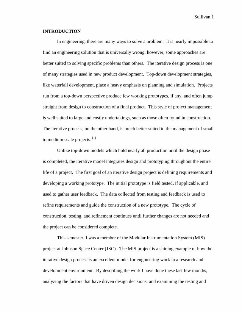
Sullivan 3
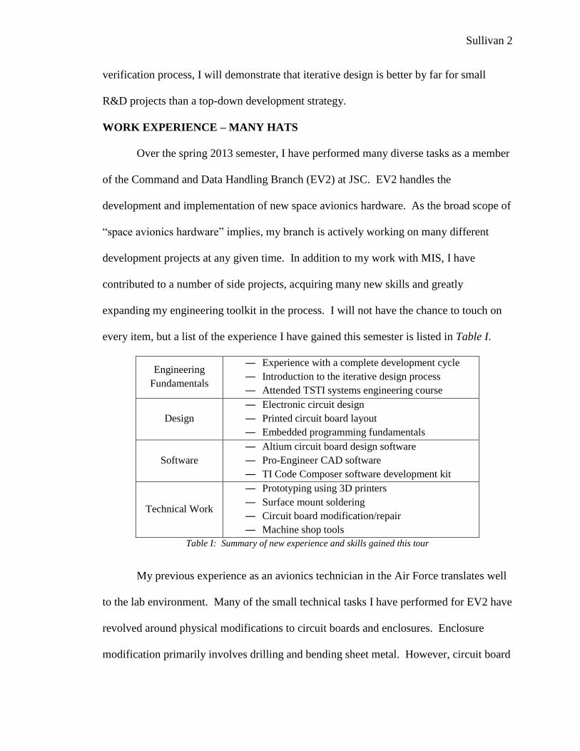
Figure 2: Georgia Tech analysis of hybrid
resistive/capacitive button functionality
modifications can be an intricate and complicated process. In situations where the circuit
paths must be modified, knives are used to cut copper traces on the surface of the board.
These traces can be extremely small; most on the MIS board are a eight thousandths of an
inch wide. Once the traces are cut, jumper wire is soldered to components on the board
to create new electrical paths. Examples of jumper wire soldering and trace cutting can
be seen in Figure 1. Due to the delicate nature of the work, some circuit board
modifications can take many hours to complete.
In addition to technical work, I have had the opportunity to directly involve
myself in the prototyping process. Early in my
tour, I worked closely with a JSC engineer in
the emerging field of wearable electronics.
Building upon the work of Georgia Tech
researchers [2]
, we constructed a working proof
of concept of a hybrid resistive/capacitive
button using an Arduino prototyping kit, a box
of electrical components, and a few wires.
Figure 1: A pair of integrated circuits, using 30 gauge wires to modify current paths. A cut trace, as seen
through a microscope (right)
Sullivan 4
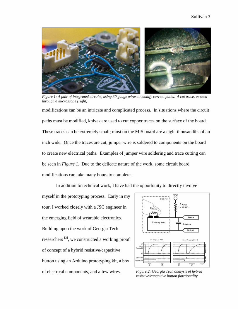
The primary challenge in
the field of wearable technology is
integrating rigid electronic
components with flexible fabrics.
The Georgia Tech-inspired hybrid
button eliminates this problem
almost entirely by moving all of the
electronic components away from
the physical button. The button itself is simply a pair of wires that registers a “press”
when a finger comes into contact with both at the same time. Note in Figure 3, how the
electronic components are not located anywhere near the button itself. These
components can be mounted anywhere on or, more importantly, off the garment. Now
that the proof-of-concept has been constructed, tested, and verified, it will be trivial for
NASA engineers to move forward with a prototype which incorporates conductive thread
woven into a garment.
As a final technical assignment, I was asked to develop a new revision of the
Modular Instrumentation System enclosure. The current enclosure is costly and, as with
any engineering design, there is always room for refinement. After learning to use the
modeling software, I simplified the existing enclosure by redesigning individual pieces to
be location and orientation agnostic. That is, rather than have unique parts for the top,
bottom, left, and right of the box, there are simply universal “end” and “side” pieces. By
reducing the number of unique parts and decreasing the complexity of the design, I was
able to cut the cost of manufacture by nearly 25%.
Figure 3: Prototype electronic textile button. Note that the
button is only the two white wires, while the rest of the
components are located on the "distant" breadboard.
Sullivan 5
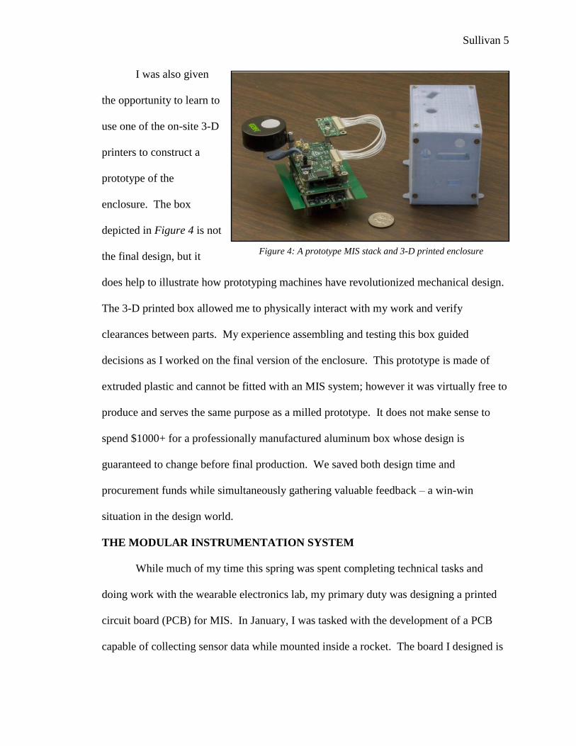
I was also given
the opportunity to learn to
use one of the on-site 3-D
printers to construct a
prototype of the
enclosure. The box
depicted in Figure 4 is not
the final design, but it
does help to illustrate how prototyping machines have revolutionized mechanical design.
The 3-D printed box allowed me to physically interact with my work and verify
clearances between parts. My experience assembling and testing this box guided
decisions as I worked on the final version of the enclosure. This prototype is made of
extruded plastic and cannot be fitted with an MIS system; however it was virtually free to
produce and serves the same purpose as a milled prototype. It does not make sense to
spend $1000+ for a professionally manufactured aluminum box whose design is
guaranteed to change before final production. We saved both design time and
procurement funds while simultaneously gathering valuable feedback – a win-win
situation in the design world.
THE MODULAR INSTRUMENTATION SYSTEM
While much of my time this spring was spent completing technical tasks and
doing work with the wearable electronics lab, my primary duty was designing a printed
circuit board (PCB) for MIS. In January, I was tasked with the development of a PCB
capable of collecting sensor data while mounted inside a rocket. The board I designed is
Figure 4: A prototype MIS stack and 3-D printed enclosure
Sullivan 6
the basis for a suborbital proof-of-concept experiment, and will be a part of the first MIS
system launched into space. The precedent-setting launch will officially mark the system
as flight-proven hardware, and open it up as a viable equipment choice for missions to the
international space station and beyond [3]
.
As far as the system itself is concerned, MIS is made up of a series of small form
factor boards (3”x1.7”) that connect to each other vertically through on-board connectors.
A set of MIS boards connected together is referred to as a “stack.” Each board in a stack
serves a specific purpose and is equipment agnostic. That is, an MIS processor board is
designed to connect to any MIS sensor board, and any combination of processors and
sensors can communicate through any MIS communications board, and so on. The idea
is to create families of reusable hardware that users can pick and choose to meet their
requirements without going through the time consuming and expensive process of
developing custom electronics. New MIS hardware is still under active development, and
I am fortunate to have had the chance to join this project at such an early stage.
JOB AMPLIFICATION – DESIGNING AN MIS BOARD
I came into this tour with only a rudimentary knowledge of logic structures and
basic circuit analysis. From this perspective, designing and building a circuit board from
scratch is no small task! Over the past four months, I have not only managed to design a
prototype sensor board – I have assembled it, programmed it, tested it, and am in the
process of designing a system demonstration.
There are many steps involved in the development of a piece of hardware, and
each one is critically important. This is especially true when that hardware is expected to
fly into space. I followed an iterative process when designing this circuit board, starting
Sullivan 7
by sitting down with my project manager and establishing design requirements. Once the
requirements were established, I selected parts and designed the board. After passing
peer review, the design was sent out to be constructed by a manufacturing house. Upon
receiving the physical boards, I populated them with electronic components using
specialized equipment. As the final step in the process, I wrote microcontroller code to
test and verify my design. During testing and verification, I corrected mistakes found in
testing and tweaked the design to improve performance and the user experience. If I
were a full-time employee, the next iteration would begin with a review of the
requirements against the results of testing. In my case, however, I will pass my work off
to another engineer for the next iteration. This process of continual refinement ensures
that the final product is streamlined and free of serious design flaws at flight time.
REQUIREMENTS
Design requirements can be broken down into two broad categories: static and
dynamic. Static requirements are often the result of physical restrictions or the operating
environment. For example, all MIS boards are required to have the same form factor, and
because they are stacked, care must be taken to ensure that components do not interfere
with other boards. Additionally, the location of the connectors and screw holes that are
used to assemble the stack must be in the same location on each board. Finally, since this
hardware is intended to fly into space, it must be as small, lightweight, low-power, and
radiation-tolerant as possible. As the name implies, “static” requirements are nearly
always absolute and unalterable once set.
In software design, design requirements can be described as a moving target
because they change with user demand [4]
. Unlike software changes, however, hardware
Sullivan 8
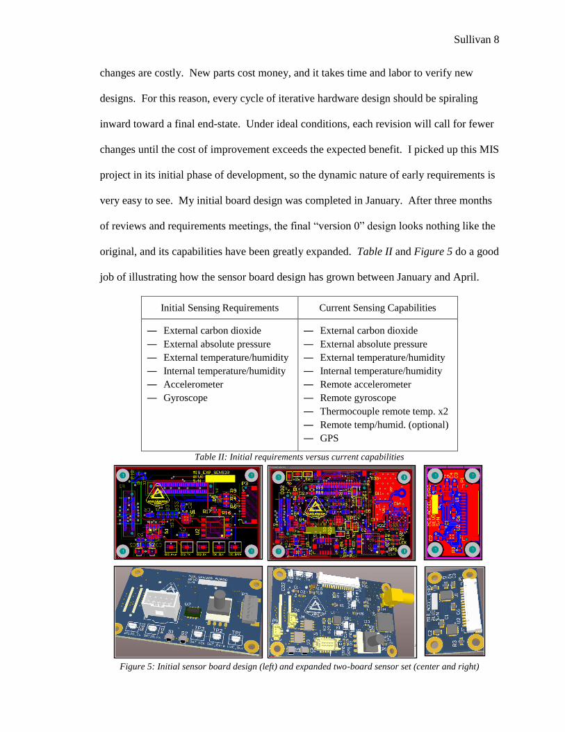
Figure 5: Initial sensor board design (left) and expanded two-board sensor set (center and right)
changes are costly. New parts cost money, and it takes time and labor to verify new
designs. For this reason, every cycle of iterative hardware design should be spiraling
inward toward a final end-state. Under ideal conditions, each revision will call for fewer
changes until the cost of improvement exceeds the expected benefit. I picked up this MIS
project in its initial phase of development, so the dynamic nature of early requirements is
very easy to see. My initial board design was completed in January. After three months
of reviews and requirements meetings, the final “version 0” design looks nothing like the
original, and its capabilities have been greatly expanded. Table II and Figure 5 do a good
job of illustrating how the sensor board design has grown between January and April.
Initial Sensing Requirements Current Sensing Capabilities
― External carbon dioxide
― External absolute pressure
― External temperature/humidity
― Internal temperature/humidity
― Accelerometer
― Gyroscope
― External carbon dioxide
― External absolute pressure
― External temperature/humidity
― Internal temperature/humidity
― Remote accelerometer
― Remote gyroscope
― Thermocouple remote temp. x2
― Remote temp/humid. (optional)
― GPS
Table II: Initial requirements versus current capabilities
Sullivan 9
COMPONENT SELECTION
Variety is an electronic designer’s best friend, but can also be their worst
nightmare. If an engineer is looking for a component that serves a specific purpose,
chances are he or she will have no trouble finding at least one. The problem is that there
are often too many to choose from. It is not uncommon to look for a particular kind of
sensor, for example, and find a mountain of parts, each one only slightly different from
its counterparts.
In situations where components are in abundance, requirements often help to
narrow down the field of candidate parts. For example, one of my sensing requirements
is to be able to take external absolute pressure readings. The sensor I select must be able
to survive in the vacuum of space – which is particularly important since not all pressure
sensors are designed to handle a true vacuum. Additionally, it must be capable of
running on 3.3 volts or less and be able to communicate digitally. Finally, it must mount
to the surface of a PCB and be equipped with a means of attaching a hose or some other
form of external measurement apparatus. In the end, my requirements narrowed my
choice of sensors from several thousand to four, and I was able to easily choose a part
that was best suited to satisfy my project’s requirements.
The selection of everything from expensive sensors to tiny microswitches were
guided by the same process. There was a great deal of research involved, and I spent
several hours on each major component, pouring over manufacturer websites and data
sheets to find parts that were best suited to the task. In some cases, using the
requirements left me with no parts to choose from. At this point, a designer must
consider which requirements are flexible enough to compromise in favor of adhering
Sullivan 10
more strictly to others. In many situations, this is the only way to find parts suited to the
job without expensive custom development.
This is called requirements trading, and an example of this can be found in the
selection of a GPS receiver for my sensor board. Even low power GPS receivers require
a lot of power to run. To find a receiver that would satisfy the MIS power requirements, I
had to find a compromise between battery life and signal quality. Low power GPS units
take much longer to lock than a standard unit, but systems which use MIS sensor
hardware will be collecting data for long periods of time. They will not require rapid
GPS response times. Therefore, if locking and tracking is sluggish, it really does not
matter. Knowing this guided me to a low-power receiver which takes a long time to lock,
but uses modern tracking technology to maintain that lock in high speed applications.
BOARD LAYOUT
Circuit board layout is one of the more complicated aspects of electronic design
work. Choosing the correct electronic components is important, and that research can be
quite time consuming; however, there are volumes upon volumes of guidelines and
considerations that must be kept in mind when laying out a circuit board. This is
especially true for sensitive radio frequency (RF) circuits. Having a large number of
board lines, or traces, further complicates matters because there are minimum spacing
requirements, especially for delicate digital signal lines. Even the simplest boards can
become very challenging to lay out if there are many traces to place.
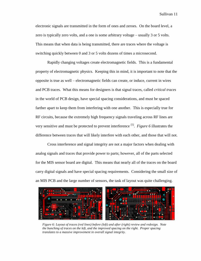
Signal integrity is the biggest concern when it comes to PCB layout. Signal
integrity means exactly what the name implies: maintaining the quality of the digital
signals that are transmitted between electronic components on the circuit boards. Digital
Sullivan 11
Figure 6: Layout of traces (red lines) before (left) and after (right) review and redesign. Note
the bunching of traces on the left, and the improved spacing on the right. Proper spacing
translates to a massive improvement in overall signal integrity.
electronic signals are transmitted in the form of ones and zeroes. On the board level, a
zero is typically zero volts, and a one is some arbitrary voltage – usually 3 or 5 volts.
This means that when data is being transmitted, there are traces where the voltage is
switching quickly between 0 and 3 or 5 volts dozens of times a microsecond.
Rapidly changing voltages create electromagnetic fields. This is a fundamental
property of electromagnetic physics. Keeping this in mind, it is important to note that the
opposite is true as well – electromagnetic fields can create, or induce, current in wires
and PCB traces. What this means for designers is that signal traces, called critical traces
in the world of PCB design, have special spacing considerations, and must be spaced
farther apart to keep them from interfering with one another. This is especially true for
RF circuits, because the extremely high frequency signals traveling across RF lines are
very sensitive and must be protected to prevent interference [5]
. Figure 6 illustrates the
difference between traces that will likely interfere with each other, and those that will not.
Cross interference and signal integrity are not a major factors when dealing with
analog signals and traces that provide power to parts; however, all of the parts selected
for the MIS sensor board are digital. This means that nearly all of the traces on the board
carry digital signals and have special spacing requirements. Considering the small size of
an MIS PCB and the large number of sensors, the task of layout was quite challenging.
Sullivan 12
BOARD MANUFACTURE AND ASSEMBLY
Within the larger iterative architecture of the MIS project, there are many
embedded iterative tasks. PCB layout is one such task: layouts are designed, reviewed,
redesigned, re-reviewed, and so on until a final design is agreed upon. In the world of
programming, these embedded iterative processes would be called “nested loops.”
Engineering is full of examples of the usefulness of iterative processes, and it is easy to
see why. Without several cycles of review and redesign, there is a good chance that
small, simple mistakes will find their way into the prototype. An unfortunate reality of
PCB design is that simple mistakes often translate to unusable boards and thousands of
wasted dollars. Once a final PCB layout is agreed upon, the design goes out to a third
party for manufacturing.
My department deals almost exclusively with prototyping. Due to the small
quantities involved in this type of work, it often falls upon us to assemble, or populate,
our circuit boards. Board population is a straightforward process. There are machines
equipped with special lifting and magnification tools, which are designed especially to
pick up and place tiny electronic components. These “pick and place” machines greatly
acceleate the assembly process. Using the machine allowed me to populate ten circuit
boards by hand, placing nearly five hundred discrete components, over the course of
several hours. Attaching these parts using hand soldering techniques is possible, but the
amount of time required would be orders of magnitude greater. Additionally, doing
anything by hand when it comes to circuit boards, especially intricate soldering work,
would create many opportunities for human error to introduce itself as a factor in the
assembly process.
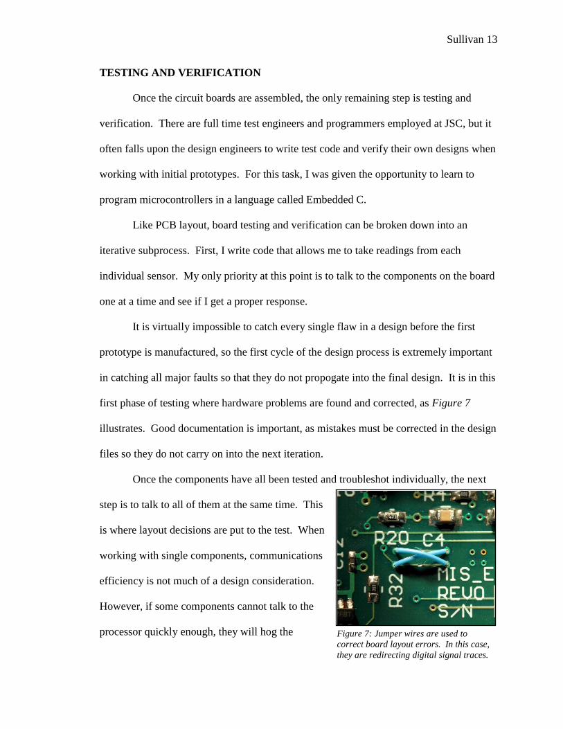
Sullivan 13
Figure 7: Jumper wires are used to
correct board layout errors. In this case,
they are redirecting digital signal traces.
TESTING AND VERIFICATION
Once the circuit boards are assembled, the only remaining step is testing and
verification. There are full time test engineers and programmers employed at JSC, but it
often falls upon the design engineers to write test code and verify their own designs when
working with initial prototypes. For this task, I was given the opportunity to learn to
program microcontrollers in a language called Embedded C.
Like PCB layout, board testing and verification can be broken down into an
iterative subprocess. First, I write code that allows me to take readings from each
individual sensor. My only priority at this point is to talk to the components on the board
one at a time and see if I get a proper response.
It is virtually impossible to catch every single flaw in a design before the first
prototype is manufactured, so the first cycle of the design process is extremely important
in catching all major faults so that they do not propogate into the final design. It is in this
first phase of testing where hardware problems are found and corrected, as Figure 7
illustrates. Good documentation is important, as mistakes must be corrected in the design
files so they do not carry on into the next iteration.
Once the components have all been tested and troubleshot individually, the next
step is to talk to all of them at the same time. This
is where layout decisions are put to the test. When
working with single components, communications
efficiency is not much of a design consideration.
However, if some components cannot talk to the
processor quickly enough, they will hog the
Sullivan 14
communications lines and bog down the entire stack. Additionally, if the electrical traces
are not spaced properly to preserve signal integrity, this is where problems will begin to
show up. Signal integrity problems often manifest as intermittent errors or erroneous
readings from sensors. In situations where such problems cannot be fixed simply through
cutting and rerouting traces, sometimes creative programming can come to the rescue and
turn a buggy board into a fully functional prototype [6]
.
Finally, once the intra-board communications have been tested and verified, the
board must be calibrated. Tests must be designed to check the accuracy of the sensors,
and if custom code must be written for specific boards to “software-calibrate” the
sensors, this is when it will be done.
Once calibration testing is complete, the prototype can be considered finished. At
this point, the design should be tested in field conditions or with users to ensure that the
designer has properly met their needs. At the time of writing this paper, I am currently
working on writing a user interface so that others can interact with my design and offer
valuable feedback which will be used to guide the next iteration or the process.
ITERATIVE DESIGN IN RESEARCH AND DEVELOPMENT
There is an old military saying which states that even the most thoughtful, best
laid battle plans never survive contact with an enemy. While there are no battles being
fought within circuit boards, this sentiment holds true in design work. No matter how
many eyes look over a design, no matter how many times it is reviewed, there will be
uncaught mistakes. These mistakes are just a part of the process and should be
expected[7]
. What makes prototyping extremely important is the fact that a large
majority of these mistakes become glariningly obvious in the testing and verification
Sullivan 15
process, and they must be corrected before the design can be verified. In this sense, it can
be said that “no circuit board design flaw survives contact with testing and verification.”
The lack of regular feedback and verification throughout the design process is one
major failing of top-down waterfall development models. Top-down development works
well in situations where costs are high and an overarching design paradigm has already
been established – such as in bridge building. Bridge designers do not have to design a
new type of bridge from scratch every time because there are already operating models to
base their work upon. However, in a research and development environment where there
are new products and ideas being developed, it is much better to start with a rough initial
prototype that meets the basic requirements, and then spiral down toward an end state
that meets all of the needs of the end-user.
Without regular testing and feedback, it can be very difficult to tell if the end
product will be something that the customer can actually use. This is where iterative
development shines, as it provides designers with regular feedback that helps to guide
their designs in the right direction. In new product development, simulation and analysis
is almost never a better choice than hardware testing and user feedback.
CONCLUSION
Simulation and analysis is no substitution for real testing and physical interaction
is no substitution. It is for this reason that the iterative design process is well suited to a
development environment where new products are being created. The MIS project is still
in its infancy. The constant stream of feedback collected from users and tests ensures
that every revision results in a prototype that spirals in toward meeting the requirements
of its customers without major design flaws. The iterative design process is quite

Sullivan 16
obviously the right choice for research and development projects, and I am thankful to
have had the chance to have experienced it firsthand.
Sullivan 17
REFERENCES
[1] Kroll, P. (2004, April 16). Transitioning from waterfall to iterative
development. Retrieved from IBM Developerworks:
http://www.ibm.com/developerworks/rational/library/4243.html
[2] Gilliland, S. (2010). The Textile Interface Swatchbook: Creating Graphical
User Interface-like Widgets with Conductive Embroidery. International Symposium on
Wearable Computers (pp. 1-8). Seoul, South Korea: Georgia Institute of Technology.
[3] Yim, H. (2013, 01 20). Conversations with Hester. (G. Sullivan, Interviewer)
[4] Larson, K. S. (2009). Applied Space Systems Engineering. In K. S. Larson,
Applied Space Systems Engineering (pp. 460-463). Boston: McGraw Hill.
[5] Herring, C. (2013, Jan-Apr). Conversations with Christy during Circuit Board
Layout Review. (G. Sullivan, Interviewer)
[6] Kim, A. (2013, Apr 23). Conversations with Alex about Software Repair. (G.
Sullivan, Interviewer)
[7] Wade, R. (2013, April 19). Conversations with Randy over PCB Design
Mistakes. (G. Sullivan, Interviewer)