the path to exascale - gtc on-demand featured...
TRANSCRIPT

The Path to ExaScale Bill Dally | Chief Scientist and SVP, Research NVIDIA | Professor (Research), EE&CS, Stanford

Scientific Discovery and Business Analytics
Driving an Insatiable Demand for More Computing Performance

The Exascale Challenge
Sustain 1EFLOPs on a “real” application
Power less than 20MW
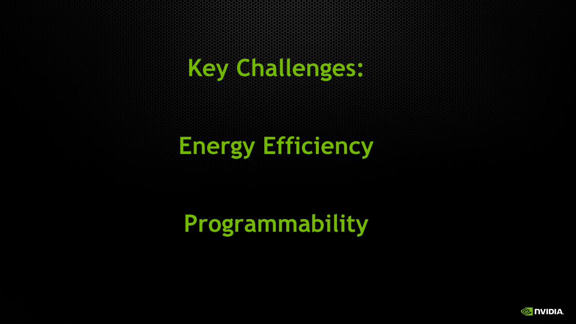
Key Challenges:
Energy Efficiency
Programmability

18,688 NVIDIA Tesla K20X GPUs
27 Petaflops Peak: 90% of Performance from GPUs
17.59 Petaflops Sustained Performance on Linpack
~2.5GFLOPS/W
TITAN
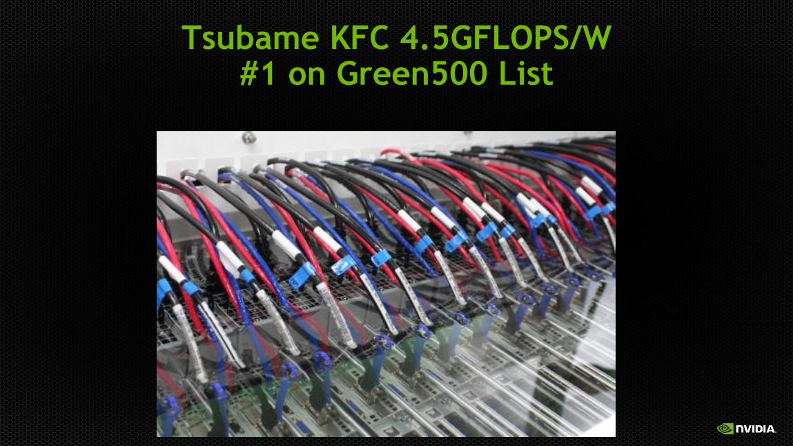
Tsubame KFC 4.5GFLOPS/W #1 on Green500 List

20PF 18,000 GPUs
10MW 2 GFLOPs/W ~10
7 Threads
You Are Here
1,000PF (50x) 72,000HCNs (4x)
20MW (2x) 50 GFLOPs/W (25x)
~1010 Threads (1000x)
2013
2023

20PF 18,000 GPUs
10MW 2 GFLOPs/W ~10
7 Threads
You Are Here
1,000PF (50x) 72,000HCNs (4x)
20MW (2x) 50 GFLOPs/W (25x)
~1010 Threads (1000x)
2013
2023
2017
CORAL 150-300PF (5-10x)
11MW (1.1x) 14-27 GFLOPs/W (7-14x)
Lots of Threads

Energy Efficiency
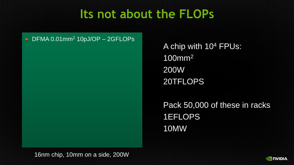
Its not about the FLOPs
16nm chip, 10mm on a side, 200W
DFMA 0.01mm2 10pJ/OP – 2GFLOPs
A chip with 104 FPUs:
100mm2
200W
20TFLOPS
Pack 50,000 of these in racks
1EFLOPS
10MW

Overhead
Locality
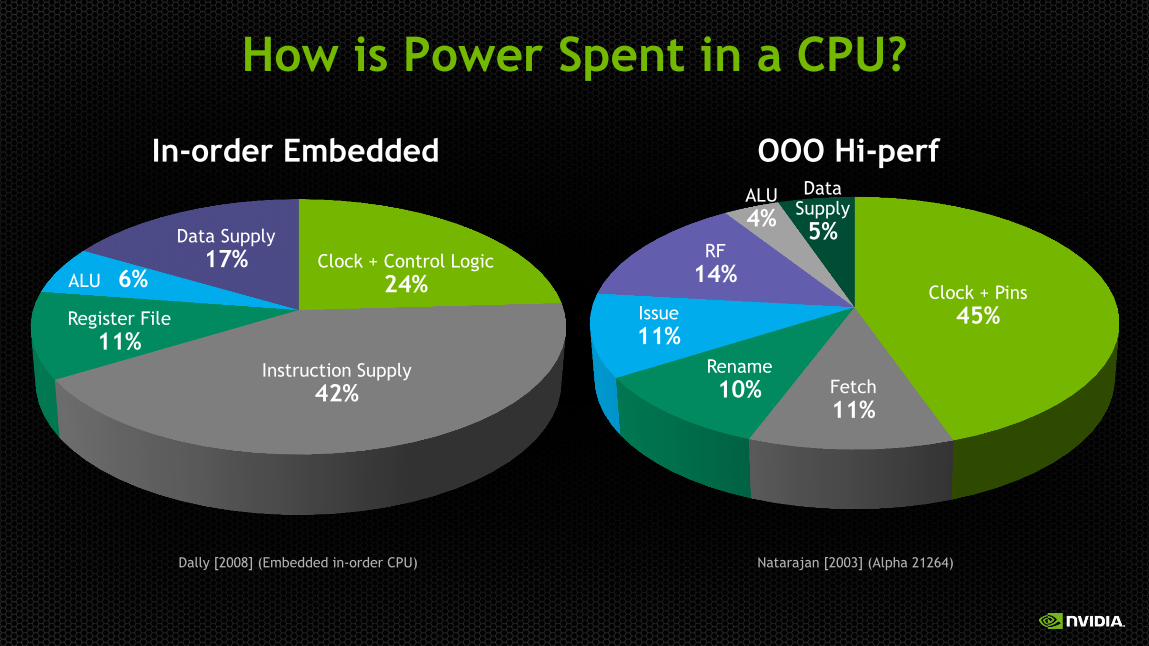
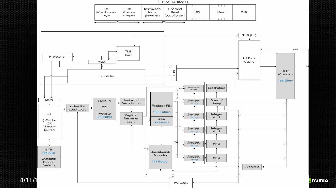
How is Power Spent in a CPU?
In-order Embedded OOO Hi-perf
Clock + Control Logic
24%
Data Supply
17%
Instruction Supply
42%
Register File
11%
ALU 6% Clock + Pins
45%
ALU
4%
Fetch
11%
Rename
10%
Issue
11%
RF
14%
Data Supply
5%
Dally [2008] (Embedded in-order CPU) Natarajan [2003] (Alpha 21264)

Overhead
980pJ
Payload
Arithmetic
20pJ
4/11/11 Milad Mohammadi 14
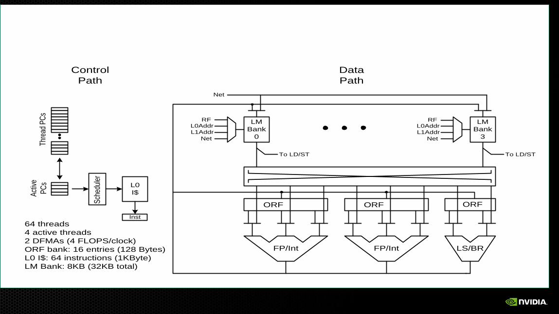
ORF ORFORF
LS/BRFP/IntFP/Int
To LD/ST
L0Addr
L1Addr
Net
LM
Bank
0
To LD/ST
LM
Bank
3
RFL0Addr
L1Addr
Net
RF
Net
Data
Path
L0
I$
Thre
ad P
Cs
Act
ive
PC
s
Inst
Control
Path
Sch
edul
er
64 threads
4 active threads
2 DFMAs (4 FLOPS/clock)
ORF bank: 16 entries (128 Bytes)
L0 I$: 64 instructions (1KByte)
LM Bank: 8KB (32KB total)

Overhead
20pJ
Payload
Arithmetic
20pJ

64-bit DP 20pJ 26 pJ 256 pJ
1 nJ
500 pJ Efficient off-chip link
256-bit buses
16 nJ DRAM Rd/Wr
256-bit access 8 kB SRAM 50 pJ
20mm
Communication Energy

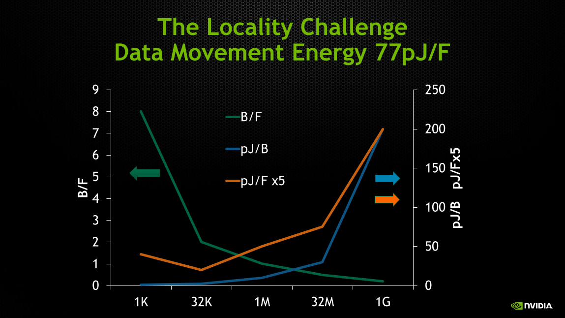
The Locality Challenge Data Movement Energy 77pJ/F
0
50
100
150
200
250
0
1
2
3
4
5
6
7
8
9
1K 32K 1M 32M 1G
pJ/B
p
J/F
x5
B/F
B/F
pJ/B
pJ/F x5

Processor Technology 40 nm 10nm
Vdd (nominal) 0.9 V 0.7 V
DFMA energy 50 pJ 7.6 pJ
64b 8 KB SRAM Rd 14 pJ 2.1 pJ
Wire energy (256 bits, 10mm) 310 pJ 174 pJ
Memory Technology 45 nm 16nm
DRAM interface pin bandwidth 4 Gbps 50 Gbps
DRAM interface energy 20-30 pJ/bit 2 pJ/bit
DRAM access energy 8-15 pJ/bit 2.5 pJ/bit
Keckler [Micro 2011], Vogelsang [Micro 2010]
Energy Shopping List
FP Op lower bound
=
4 pJ

Minimize Data Movement
Move Data More Efficiently


GRS Test Chips
Probe Station
Test Chip #1 on Board
Test Chip #2 fabricated on production GPU
Eye Diagram from Probe Poulton et al. ISSCC 2013, JSSCC Dec 2013
The Locality Challenge Data Movement Energy 77pJ/F
0
50
100
150
200
250
0
1
2
3
4
5
6
7
8
9
1K 32K 1M 32M 1G
pJ/B
p
J/F
x5
B/F
B/F
pJ/B
pJ/F x5

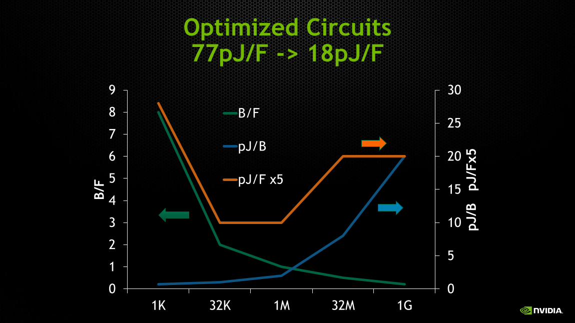
Optimized Circuits 77pJ/F -> 18pJ/F
0
5
10
15
20
25
30
0
1
2
3
4
5
6
7
8
9
1K 32K 1M 32M 1G
pJ/B
p
J/F
x5
B/F
B/F
pJ/B
pJ/F x5

Bandwidth Distribution
10% of application footprint
up to 65% of bandwidth
Can be concentrated in few data structures
Opportunities for smart data allocation and
placement in multi-level DRAM
Optimized Circuits 77pJ/F -> 18pJ/F
0
5
10
15
20
25
30
0
1
2
3
4
5
6
7
8
9
1K 32K 1M 32M 1G
pJ/B
p
J/F
x5
B/F
B/F
pJ/B
pJ/F x5

Autotuned Software 18pJ/F -> 9pJ/F
0
5
10
15
20
25
0
0.5
1
1.5
2
2.5
3
3.5
4
4.5
1K 32K 1M 32M 1G
pJ/B
p
J/F
x5
B/F
B/F
pJ/B
pJ/F x5

Simplify Programming
While Improving Locality

Parallel programming is not inherently any more difficult than serial programming However, we can make it a lot more difficult

A simple parallel program
forall molecule in set { // launch a thread array
forall neighbor in molecule.neighbors { // nested
forall force in forces { // doubly nested
molecule.force =
reduce_sum(force(molecule, neighbor))
}
}
}
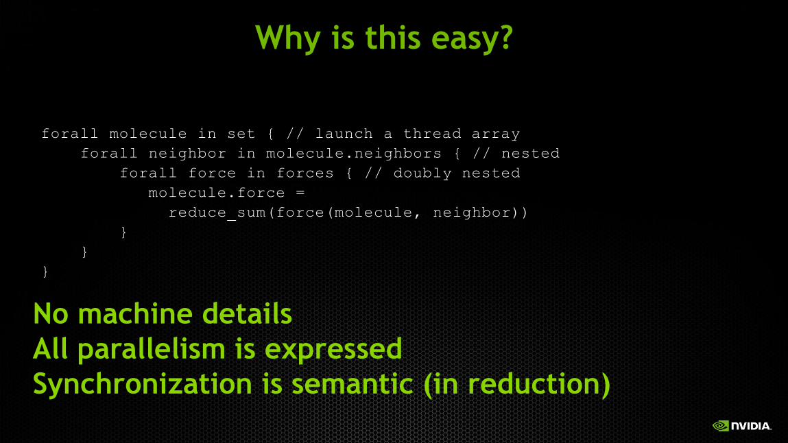
Why is this easy?
forall molecule in set { // launch a thread array
forall neighbor in molecule.neighbors { // nested
forall force in forces { // doubly nested
molecule.force =
reduce_sum(force(molecule, neighbor))
}
}
}
No machine details
All parallelism is expressed
Synchronization is semantic (in reduction)

We could make it hard
pid = fork() ; // explicitly managing threads
lock(struct.lock) ; // complicated, error-prone synchronization
// manipulate struct
unlock(struct.lock) ;
code = send(pid, tag, &msg) ; // partition across nodes

Programmers, tools, and architecture Need to play their positions
Programmer
Architecture Tools
forall molecule in set { // launch a thread array
forall neighbor in molecule.neighbors { //
forall force in forces { // doubly nested
molecule.force =
reduce_sum(force(molecule, neighbor))
}
}
}
Map foralls in time and space
Map molecules across memories
Stage data up/down hierarchy
Select mechanisms
Exposed storage hierarchy
Fast comm/sync/thread mechanisms
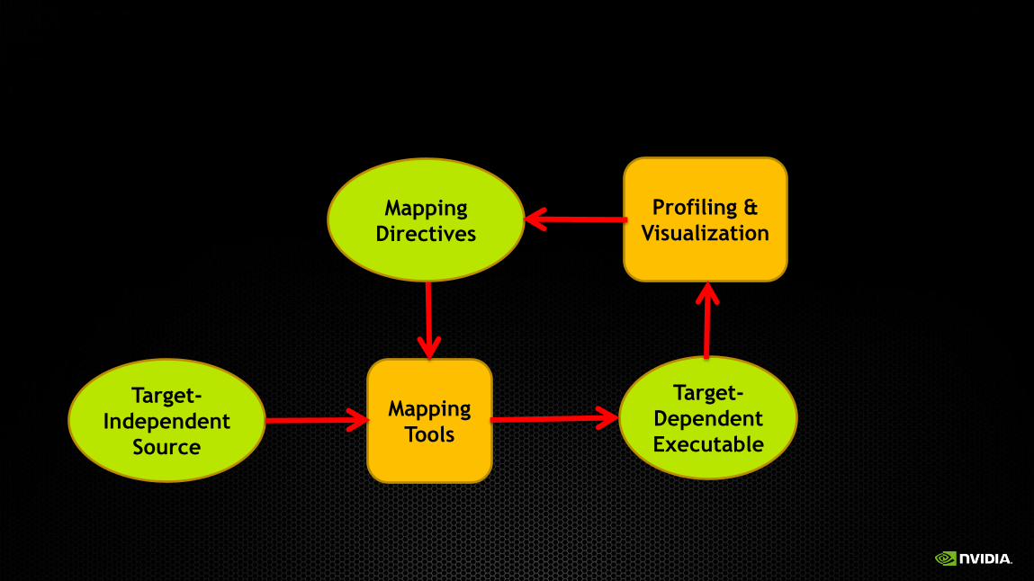
Target-
Independent
Source
Mapping
Tools
Target-
Dependent
Executable
Profiling &
Visualization Mapping
Directives

System Sketch

System Interconnect
Cabinet 0: 6.3 PF, 128 TB
System (up to 1 EF)
Cabinet 176
NoC
MC NIC
LO
C 0
LO
C 7
DRAM
Stacks
DRAM
DIMMs
NV
RAM
Node 0: 16.4 TF, 2 TB/s, 512+ GB
TO
C1
TO
C2
TO
C3
TOC0
Lane
15
Lane
0
TPC0
L20
1MB
L21
1MB
L22
1MB
L23
1MB
TP
C127
MC
Node 383
System Sketch

HPC Network
• <1ms Latency
• Scalable bandwidth
• 0.3-5% DRAM BW
• Small messages 50% @ 32B
• Global adaptive routing
• PGAS
• Collectives & Atomics
• MPI Offload
One Network
• Chip, node, system
An Enabling HPC Network
System Interconnect
Cabinet 0: 6.3 PF, 128 TB
System (up to 1 EF)
Cabinet 176
NoC
MC NIC
LO
C 0
LO
C 7
DRAM
Stacks
DRAM
DIMMs
NV
RAM
Node 0: 16.4 TF, 2 TB/s, 512+ GB
TO
C1
TO
C2
TO
C3
TOC0
Lane
15
Lane
0
TPC0
L20
1MB
L21
1MB
L22
1MB
L23
1MB
TP
C127
MC
Node 383

Co-Design

Co-Design
22.1
63.8 9.3 76.6
23
24.5
1.41
30.2
1.33 15.2
1.61 12.1
55.3 66.4
0
5
10
15
20
25
30
35
GFlops/W GOps/W
Rela
tive Im
pro
vem
ents
To E
nerg
y E
ffic
iency CNS
CoMD
Lulesh
MiniFE
SNAP
XSBench
LINPACK
Target
Tech Scaling

Summary
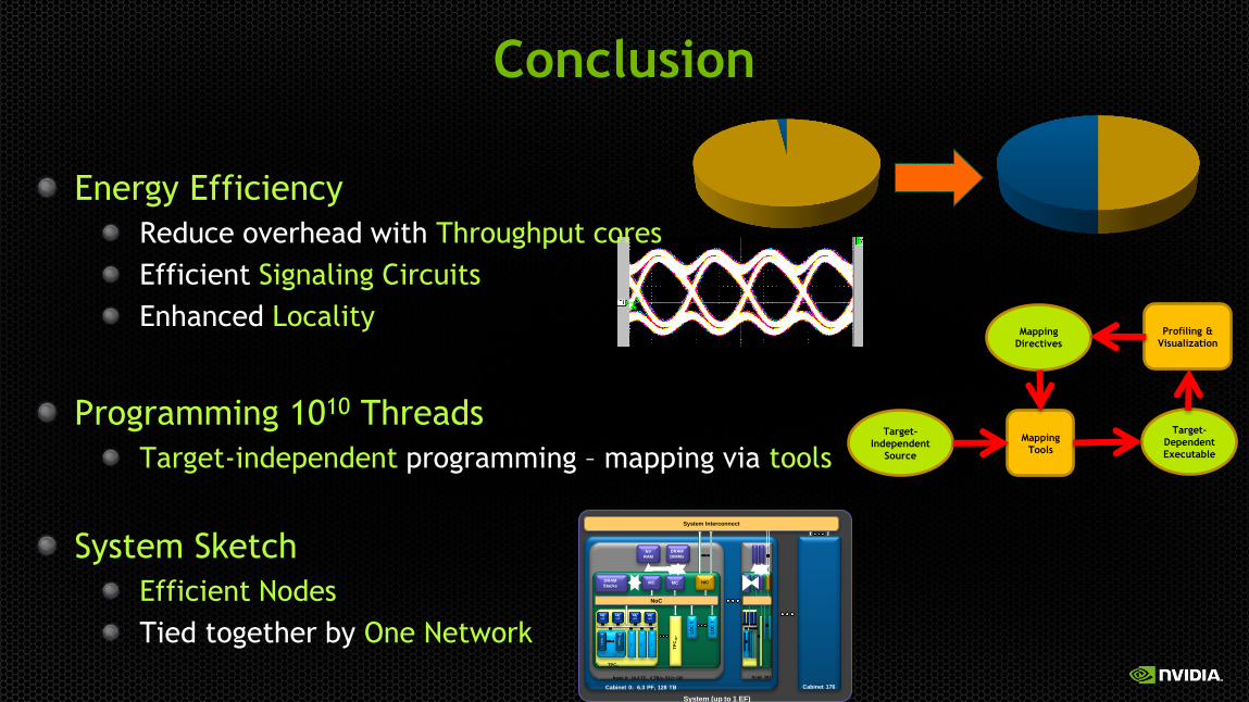
Conclusion
Energy Efficiency
Reduce overhead with Throughput cores
Efficient Signaling Circuits
Enhanced Locality
Programming 1010 Threads
Target-independent programming – mapping via tools
System Sketch
Efficient Nodes
Tied together by One Network
Target-
Independent
Source
Mapping
Tools
Target-
Dependent
Executable
Profiling &
Visualization Mapping
Directives
System Interconnect
Cabinet 0: 6.3 PF, 128 TB
System (up to 1 EF)
Cabinet 176
NoC
MC NIC
LO
C 0
LO
C 7
DRAM
Stacks
DRAM
DIMMs NV
RAM
Node 0: 16.4 TF, 2 TB/s, 512+ GB
TO
C1
TO
C2
TO
C3
TOC0
Lane
15
Lane
0
TPC0
L20
1MB
L21
1MB
L22
1MB
L23
1MB
TP
C127
MC
Node 383

“Super” Computing From Super Computers to Super Phones