the world’s best - elproscan.com · elproscan is the world’s1st commercial specm system from...
TRANSCRIPT

ElProScan SPECM System
The World’s Best
Scanning Photoelectrochemical Microscope
✓ Unique Matrix Scan with Microelectrode and Light Beam Remaining Confocal
✓ Electrochemical Signals Synchronized with Spatially Resolved Photo-Excitation
✓ Multi-Dimensional Data Obtained on the True Micron or Nano-Scale
Scanning Photoelectrochemical Microscopy
www.heka.com

❖ ElProScan is the World’s 1st commercial SPECM system from HEKA for microscopic study andimaging of photoelectrochemical processes on micron and sub-micron scale.
ElProScan - Scanning Photoelectrochemical Microscope System
❖ The innovative SPECM works for a wide range of materials and applications:
• Inorganic Semiconductors• Semiconducting Polymers
• Hybrid Nanostructures• Organic Photovoltaic Materials
• Solar to Electricity Conversion (solar cells)• Solar to Chemical Energy Conversion (Water
splitting and CO2 reduction)
• Photosterilisation, Self-Cleaning Surfaces
• Environmental (air and water) Remediation
❖ Unique system design features a Synchronized Photo-Excitation System seamlesslyintegrated with a Scanning Electrochemical Microscope (SECM) system.
Advanced SECM System from
above the sample(XYZ)
Synchronized Photo Excitation System on
the inverted bottom (F)
❖ The Modular Optical Train is compatible with most excitation light sources (LED / Laser/ Xeonarc lamp).
❖ The incident light beam spot size may be adjusted by users, ranging from ca. 1µm – 900µm.❖ The vertically mounted scanning probe remains confocal with light beam during scanning; one
scan of XY-stage yields multi-channel optical, physical and electrochemical data (3D/4D/5D…)simultaneously.
Illustrative cartoon shows a transparent substrate
2
Legend:1: Objective Lens2: Beam-Splitter3: 90° Mirror4/5/8: Special Optical Lenses6: C-mount Adapter7: Variable Field Stop9: Light Guide Adapter
A general scheme for the SPECM design

PG618USB – The Perfect Bipotentiostat for Photoelectrochemical Imaging
3
Features
• The Ultra Bipotentiostat PG618USB is designed and optimized to support cutting-edge scanningprobe experiments. The amplifier-1 channel supports larger current ranges that’re suitable forconnecting with a bulk sample electrode. The amplifier-2 features a low noise ultra-sensitivepreamplifier channel for controlling or sensing voltage and/or current of the micro-probeworking electrode.
Each HEKA SPECM system includes the best-in-class Bipotentiostat (PG618USB) for studying nanoscale electrochemical signals.
• Best-in-class current resolution of 0.15 fA in the lowest 5pA range (with current noise < 3.5 fAat 15 Hz bandwidth in 5 pA range)
• Built-in 16 bit, 200 kHz AD/DA interface with 5 μs shortest sample interval
• Additional low-current preamplifier channels can be scaled up to support triple or quadrupleWorking Electrodes
• Additional Auxiliary I/O ports empower the control of external equipment (such as light source,filter wheels, cameras, etc.)
• Can be used as a standalone Workstation for a wide range of traditional electroanalyticalapplications, including electrochemical sensing of single nanoparticles & single molecules
• Optional upgrade with high current boosters up to±50 A range
Amplifier-2
Amplifier-1
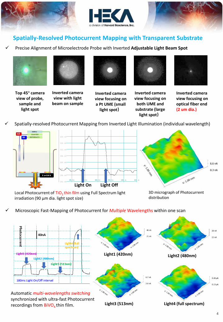
✓ Precise Alignment of Microelectrode Probe with Inverted Adjustable Light Beam Spot
✓ Microscopic Fast-Mapping of Photocurrent for Multiple Wavelengths within one scan
Spatially-Resolved Photocurrent Mapping with Transparent Substrate
Inverted camera view focusing on optical fiber end (2 um dia.)
Top 45° camera view of probe,
sample and light spot
Inverted camera view with light
beam on sample
Inverted camera view focusing on
both UME and substrate (large
light spot)
Inverted camera view focusing on a Pt UME (small
light spot)
292. nA
296. nA
300. nA
304. nA
308. nA
312. nA
316. nA
320. nA
20.0 s 40.0 s 60.0 s 80.0 s 100. s 120. s
Local Photocurrent of TiO2 thin film using Full Spectrum light irradiation (90 µm dia. light spot size)
Light On Light Off
3D micrograph of Photocurrent distribution
✓ Spatially-resolved Photocurrent Mapping from Inverted Light Illumination (individual wavelength)
Light1 (420nm) Light2 (480nm)
Light3 (513nm) Light4 (full spectrum)
Automatic multi-wavelengths switching synchronized with ultra-fast Photocurrent recordings from BiVO4 thin film.
4
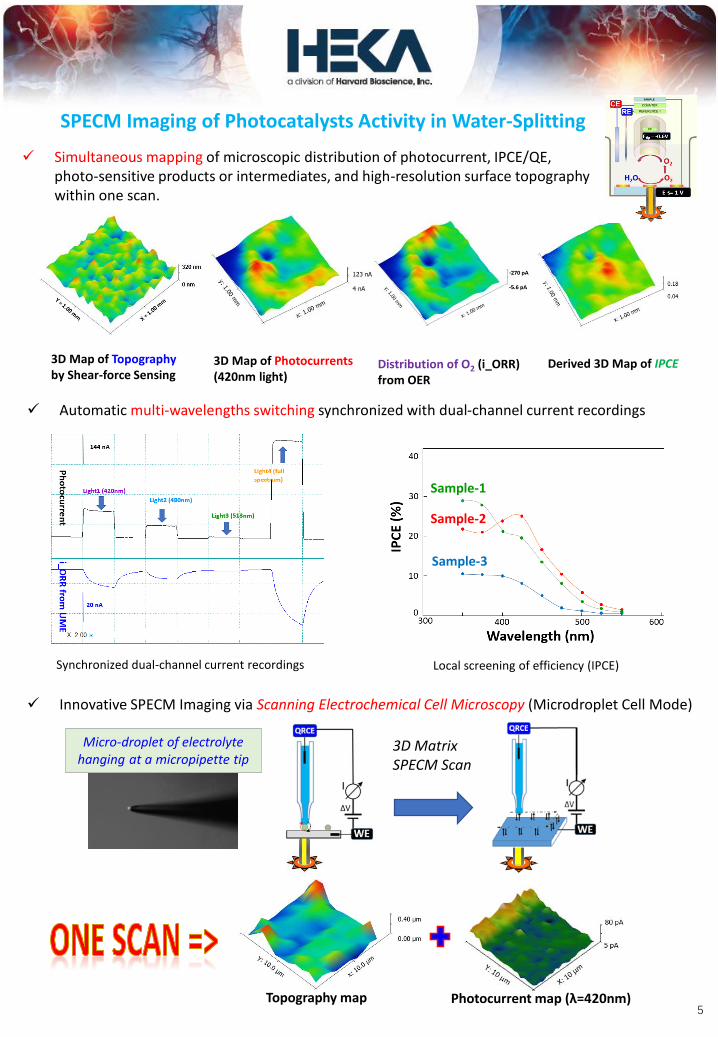
✓ Simultaneous mapping of microscopic distribution of photocurrent, IPCE/QE, photo-sensitive products or intermediates, and high-resolution surface topography within one scan.
✓ Automatic multi-wavelengths switching synchronized with dual-channel current recordings
SPECM Imaging of Photocatalysts Activity in Water-Splitting
3D Map of Photocurrents(420nm light)
Distribution of O2 (i_ORR) from OER
Derived 3D Map of IPCE
Local screening of efficiency (IPCE)Synchronized dual-channel current recordings
Sample-1
Sample-2
Sample-3
✓ Innovative SPECM Imaging via Scanning Electrochemical Cell Microscopy (Microdroplet Cell Mode)
Micro-droplet of electrolyte hanging at a micropipette tip
3D Matrix SPECM Scan
Topography map Photocurrent map (λ=420nm)5
3D Map of Topography by Shear-force Sensing

Working with Non-transparent Substrate via Opto-Pipette
✓ 2018 new system supports optical fiber couplings with Opto-micropipette techniques via SICM or SECCM configurations.
Opto-pipette used in Scanning Ion Conductance Microscopy mode
Top camera view of Opto-micropipette tip and mirror image from a wafer sample
✓ Local Photocurrent (~fA resolution) and Topography (~nm resolution) can be mapped simultaneously within one scan
✓ Improved light-beam spatial resolution vs. bulk mode (e.g. 1~2 µm vs 90 µm dia. spot)
✓ Much improved s/n ratio and ultra-low noise in Photocurrent (e.g. pA vs. nA)
✓ Only a small local spot is in contact with electrolyte at a time
✓ Multiple wavelengths of light can be automatically switched and measured in one user-defined Matrix Scan
Benefit & Novelty
Opto-pipette used in Scanning Electrochemical Cell Microscopy mode
6
Localized top-illumination mode via a quartz glass microprobe is compatible with Shear-force Topography-Sensing technique
Localized photocurrent measurements from multi-wavelength illuminations, obtained from Synchronized Optopipette-SECCM experiments.

The Most Featured and Versatile Accessories for SPECM
◼ Microelectrode Polishing Machine
◼ Electrochemical Cell Stage Insert with Temperature Control and Gas Purging
◼ Microelectrodes (Pt / Au / Carbon)
200 nm – 25 µm dia.
◼ Holders for Microelectrodes, Micropipettes and SMA-Fibers
◼ Various Light Sources & Filters
◼ Vibration-isolation & Shielding Device
7

Components and Items Technical Specifications
Po
sition
ing Syste
m w
ith In
tegrate
d M
icrosco
pe
Op
tics
X/Y/Z/F 4D positioning system4-Axis DC servo motors with Z-axis piezoelectric system (XY-axis carries sample inscanning; Z-axis carries microprobe, and F-axis drives objective lenses for precise focus).
Resolution of X/Y/Z Axis Linear Encoder of each motor axis = 2.5 nm resolution (all closed-loop controlled); 1.5nm resolution for the Z-axis piezo module; XY-scan resolution = 10 nm with 4 timesoversampling algorithm to ensure accuracy
X/Y/Z/F Axis Travel Range Automatic motor-scan range: X = 100 mm, Y = 75 mm, Z and F = 50 mm.Z-axis piezo range = 100 µm (closed-loop controlled)A manual translator unit extends XY range to additional 12 mm.
4D External JoystickFor X/Y/Z/F manual control with sub-micron accuracy; may operate in precise-slowmotion and coarse-fast motion.
Integrated Microscope Optics
The inverted optical train contains a motorized focus drive, epi-fluorescence opticsin Kohler configuration (with a variable field stop) and special coupling to a liquidlight guide, camera port with C-mount, an optional Filter cube holder, and slide-inbeam splitter and a mirror cube.Additional fixed-spot size illumination path with coupling to a FC/PC fiber isincluded. Optional objectives (4x up to 100x) can be mounted in a 6-position turretnose piece. Microscope optics transmits light of wavelength above 330nm.
Optional UpgradeTop 45° camera system may record and view the microprobe and sample surface in prepositioning, greatly facilitating Z/F-axes alignment and pre-scan preparations.
Bip
ote
ntio
stat Wo
rkStation
Voltage Range / Resolution ± 10V (in single amplifier mode) / 610 nV
Current Ranges ±20 nA to ±100 mA (Amp-1); ±5 pA to ±2 μA (Amp-2; total 18 ranges available)
Max. Current Resolution 0.15 fA in 5pA range (Amp-2);0.61 pA in 20nA range (Amp-1)
Noise in Current RMS value < 3.5 fA (at 15 Hz bandwidth in 5 pA range of Amp-2)
DAC Interface 16-bit / 5 µs fastest pulse / 200 kHz sampling rate
Optional Upgrade
(1)Current Booster for extending max. current range to ±50 A(2)External EIS measurement module (10 μHz – 1 MHz)
(3) Scanning Kelvin Probe system available as an add-on module
ElProScan SPECM System Configurations and Specifications
Ph
oto
-Excitation
System
Synchronized Multi-Wavelength Excitation System
Standard package includes: 300W Xenon arc lamp, shuttered 10-position filter wheel,fused silica light guide, 10 bandpass filters with 10nm bandwidth in the range of 350nmto 800nm, 1 neutral density filter).
Light Guide to Fiber Coupler Kit
Used for connecting a light guide with 5mm OD and 20mm length fitting to a SMA typeoptical fiber for the fixed spot-size illumination path.
Opto-Pipette Holder KitA special pipette holder with a straight optical port (SMA type) used for coupling a HEKACannula to an optical fiber for combined top-illumination in SICM/SECCM experiments.
Optional UpgradeSpecial customization is available for adding Synchronized Fluorescence Imaging
module.8

ElProScan SPECM Supported Techniques and Applications*
Supported Techniques Key Features Main Application Examples
SECM for localized 2D/3D imaging and spectroscopic measurements
Supports all existing SECM operation modes (Feedback; Generation-Collection; Redox-Competition, AC-SECM, etc.)
Mapping surface electrochemical activities of various samples and systems (e.g. biological sensors, live cells, molecular transport at porous membranes, electro- & photo-catalysts, local Corrosion processes, liquid/liquid charge transfer, micro-fabrication & micro-patterning of surface)
Simultaneous Surface Topography Mapping
Shear-force based Constant Distance scan in synchronization within SECM or AC-SECM scans (via advanced non-contact hopping mode)
(i) In situ imaging of sample’s height profiles and topography. (ii) Real-time surface-tracking of height/volume for thin-films.
Scanning Photoelectrochemical Microscopy (SPECM)
(a) Precise synchronization of SECM with multi-wavelength photo-illumination at variable controlled spot-sizes.
(b) Multi-dimensional data recordings via automated Protocol-controlled Matrix Scan.
(c) Flexible optical designs are suited for both transparent and non-transparent samples.
(d) Spatially-resolved optical and electrochemical probe coupling reaches sub-micron resolution.
(e) Versatile optical configurations support the addition of a UV-VIS-IR spectrometer via optical fiber coupling.
(i) Simultaneous microscopic imaging of localized photocurrents, IPCE/QE distribution, and photoactive intermediates or products within a single 2D/3D SECM scan.
(ii) High throughput screening of Photocatalysts via synchronized multi-wavelength excitations and multi-channel data recordings.
(iii) Localized studies of photoelectrochemistry(e.g. Localized Photocurrent Spectroscopy; kinetics study of electron-hole recombination; Spectral Resolved Transmittance / Absorbance Spectroscopy* vs. Voltage, Current, or Time)
* requires fiber-coupled spectrometers
Scanning Ion Conductance Microscopy (SICM)
(a) Three modern operation modes of SICM are supported: AC- and DC- hopping mode, and Bias-Modulated SICM.
(b) Unique probe design allows the use of Opto-pipette to combine photo-excitations with SICM.
(i) Non-destructive high-resolution topography imaging is widely suited for all delicate and soft sample surfaces in electrolyte.
(ii) Simultaneous in situ mapping of surface charge and topography via Bias-Modulated SICM.
(iii) *Simultaneous microscopic mapping of topography and photocurrents/IPCE/QE for photoactive materials.
* Requires Opto-pipette kit and light illumination controls.
Scanning Electrochemical Cell Microscopy (SECCM) and Scanning Microcapillary Contact Method (SMCM)
(a) Users may control the probe size and the spatial resolution of the scanned area (i.e. nano-/micro-pipette tip can be prepared by users).
(b) User-defined protocol script may automate a highly complex Matrix Scan with multi-dimensional data recorded.
(c) SECCM and SMCM set-up is fully compatible with photo-illumination from top and inverted optics, thus extending the schemes of experimenting in SPECM.
(d) Unique Opto-pipette holder supports the use of various combinations of bi-functional probes: such as SECM-SICM probes; Optical illumination-SICM probes; Optical illumination-SECM probes, etc.
(i) Spatially-resolved local electrochemical analysis of photo-catalysts, electro-catalysts and conductive polymers.
(ii) Simultaneous mapping of depth profiles and localized corrosion potentials.
(iii) Nanoscale mapping of redox activity of Li-ion battery cathodes materials.
(iv) Combined SPECM imaging* with simultaneous topography mapping
* Requires Opto-pipette kit and light illumination controls.
* Please also refer to HEKA’s Full ElProScan Brochure for more technical details. 9

© 1997-2018 HEKA Elektronik Dr. Schulze GmbH - a division of Harvard Bioscience
Germany HeadquartersHEKA Elektronik Dr. Schulze GmbHWiesenstraße 71D-67466 Lambrecht/PfalzGermanyPhone: +49 (0)6325 9553-0Fax: +49 (0)6325 9553-50
USA HeadquartersHEKA Instruments Inc.84 October Hill RdHolliston, MA 01746USAToll free:+1 800 272 2775Phone: +1 508 893 8999Fax: +1 508 429 5732
China OfficeHarvard Bioscience (Shanghai) Co., Ltd.Room 8C, Zhongxi Tower, 121 Jiangsu Road, Changning District, Shanghai, China, 200050Tel: +86 21-6226 0239Email: [email protected]
General Notes:Product names, models and pictures used herein are for identification purposes only and may be trademarks of their respective owners. The copyrightof the professional terminology name involved is owned by the original author and related commercial entities. HEKA disclaims any and all rights inthose marks. The technical parameters and specifications of HEKA products are subject to the final sales agreement or contract. HEKA reserves the rightto change the product parameters caused by the progress of technology and product development. Any product manufactured and sold by HEKA shallnot be used for human-related lab research or clinical treatment purposes; HEKA reserves the right to be exempt from liability for personal injury andfinancial loss caused by the incorrect operation of any HEKA equipment.。
Please contact HEKA for ElProScan SPECM at:
[email protected]@HEKA.com
10