thermoelectric generator based on carbon...
TRANSCRIPT
i
Thermoelectric Generator based on Carbon
nanotubes
By
Zakaria SAADI
University of Surrey
Department of Electronic Engineering
Faculty of Engineering and Physical Sciences
University of Surrey
Guildford, Surrey, GU2 7XH, UK
September 2018
University of Surrey
ii
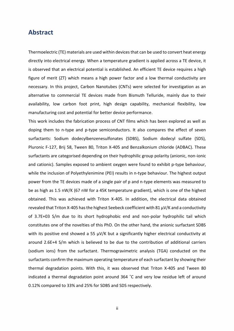
Abstract
Thermoelectric (TE) materials are used within devices that can be used to convert heat energy
directly into electrical energy. When a temperature gradient is applied across a TE device, it
is observed that an electrical potential is established. An efficient TE device requires a high
figure of merit (ZT) which means a high power factor and a low thermal conductivity are
necessary. In this project, Carbon Nanotubes (CNTs) were selected for investigation as an
alternative to commercial TE devices made from Bismuth Telluride, mainly due to their
availability, low carbon foot print, high design capability, mechanical flexibility, low
manufacturing cost and potential for better device performance.
This work includes the fabrication process of CNT films which has been explored as well as
doping them to n-type and p-type semiconductors. It also compares the effect of seven
surfactants: Sodium dodecylbenzenesulfonates (SDBS), Sodium dodecyl sulfate (SDS),
Pluronic F-127, Brij 58, Tween 80, Triton X-405 and Benzalkonium chloride (ADBAC). These
surfactants are categorised depending on their hydrophilic group polarity (anionic, non-ionic
and cationic). Samples exposed to ambient oxygen were found to exhibit p-type behaviour,
while the inclusion of Polyethylenimine (PEI) results in n-type behaviour. The highest output
power from the TE devices made of a single pair of p and n-type elements was measured to
be as high as 1.5 nW/K (67 nW for a 45K temperature gradient), which is one of the highest
obtained. This was achieved with Triton X-405. In addition, the electrical data obtained
revealed that Triton X-405 has the highest Seebeck coefficient with 81 µV/K and a conductivity
of 3.7E+03 S/m due to its short hydrophobic end and non-polar hydrophilic tail which
constitutes one of the novelties of this PhD. On the other hand, the anionic surfactant SDBS
with its positive end showed a 55 µV/K but a significantly higher electrical conductivity at
around 2.6E+4 S/m which is believed to be due to the contribution of additional carriers
(sodium ions) from the surfactant. Thermogravimetric analysis (TGA) conducted on the
surfactants confirm the maximum operating temperature of each surfactant by showing their
thermal degradation points. With this, it was observed that Triton X-405 and Tween 80
indicated a thermal degradation point around 364 ˚C and very low residue left of around
0.12% compared to 33% and 25% for SDBS and SDS respectively.

iii
In regard to the thermal behaviour of the CNT samples, it was revealed that CNT films with
lengths above 1 cm showed heat losses due to emissivity, therefore, making longer films was
deemed inefficient.
Finally, a TE device is made from the best performing surfactant (Triton X-405) because of its
optimum power factor, with 6 pairs of p and n type semiconducting CNT films. This device
was used for a motorcycle exhaust in order to simulate heat waste harvesting which resulted
in a ~ 42 mV output voltage at ~ 87 ⁰C temperature difference. This means that many
alternating pairs of p-n devices are required to achieve a high output power.
iv
Declaration of originality
I confirm that the submitted work is my own work and that I have clearly identified and fully
acknowledged all material that is entitled to be attributed to others (whether published or
unpublished). Any ideas, data, images or text resulting from the work of others are identified
as such and attributed to the original author in the text, figure captions or the bibliography. I
agree that the University may submit my work to means of checking this, such as the
plagiarism detection service Turnitin® UK. I confirm that I understand that assessed work that
has been shown to have been plagiarised will be penalised.
Author Signature: Date: 25/01/2019

v
Acknowledgements
First foremost, I am very grateful to my supervisors: Prof. Ravi Silva, Dr. Vlad Solojan and Dr.
José V. Anguita for their invaluable guidance and support to help me perform to the best of
my ability throughout these 4 years of my PhD project.
I would like to thank Dr Simon King, Ishara Dharmasena, Dr Christos Melios, Dr Imalka
Jayawardena, Dr James Clark, Dr Muhammad Ahmad, and all the lab technicians who have
helped a lot in my time at the ATI by providing me with support and guidance in my project.
Finally, and most importantly, I thank my parents for their financial support and my brother,
who have always been supportive by encouraging me and motivating me in doing a PhD
project.
vi
Conference presentations
“Thermoelectric properties of films based on carbon nanotubes”. Zakaria Saadi, José V.
Anguita, Vlad Stolojan and S. Ravi P. Silva. (Oral presentation at the EMRS conference
meeting, Warsaw, Poland, September 2016)
“Thermoelectric properties and PTCVD growth of CNTs”. Zakaria Saadi, José V. Anguita, Vlad
Stolojan and S. Ravi P. Silva. (Oral presentation at ESPRC Thermoelectric Network UK
Meeting, Glasgow, Scotland, October 2016)
“Thermoelectric devices based on carbon nanotubes”. Zakaria Saadi, Simon King, Vlad
Stolojan, José V. Anguita, and Ravi Silva. (Poster presentation at Inno LAE conference,
Genome campus, Cambridge, UK, January 2018)
vii
Contents Abstract...................................................................................................................................... ii
Declaration of originality ......................................................................................................... iv
Acknowledgements ................................................................................................................... v
Conference presentations ........................................................................................................ vi
List of Figures ............................................................................................................................. x
List of Tables ........................................................................................................................... xvi
Abbreviations and Acronyms ................................................................................................ xvii
Introduction and objective ................................................................................................ 1
1.1 Background to the project .......................................................................................... 1
1.2 Structure of the thesis ................................................................................................. 5
Theory and literature review ............................................................................................. 8
2.1 Introduction................................................................................................................. 8
2.2 Theory of thermoelectricity ........................................................................................ 9
2.3 Figure of merit ZT (TE generation and Refrigeration efficiency) .............................. 13
2.4 Solid state materials: Metals, semiconductors and insulators ................................. 18
2.5 Fermi level ................................................................................................................. 20
2.6 Inorganic thermoelectric materials ........................................................................... 23
2.6.1 Bismuth Telluride (Bi2Te3) and other materials ................................................. 23
2.7 Organic thermoelectric materials ............................................................................. 27
2.7.1 Introduction to carbon nanotubes .................................................................... 27
2.7.2 CNT synthesis ..................................................................................................... 30
2.7.3 CNT Properties ................................................................................................... 34
2.7.4 CNT dispersion/functionalization ...................................................................... 36
2.7.5 Surfactant selection ........................................................................................... 38
2.8 Optimisation of Thermoelectric properties .............................................................. 41
2.8.1 Increasing the power factor ............................................................................... 41
2.8.2 Minimising thermal conductivity ....................................................................... 42
2.9 Applications of thermoelectric materials .................................................................. 44
2.9.1 Solar thermal energy generation ....................................................................... 47
2.10 Summary ................................................................................................................... 48
Characterisation techniques ............................................................................................ 50
3.1 Electrical conductivity measurement ........................................................................ 50
viii
3.1.1 The Van der Pauw method ................................................................................ 52
3.1.2 Transmission line measurement ........................................................................ 55
3.2 Seebeck coefficient measurement ............................................................................ 57
3.3 Scanning Electron Microscopy .................................................................................. 67
3.4 Raman Spectroscopy ................................................................................................. 68
3.5 UV-VIS Spectroscopy ................................................................................................. 73
3.6 Thermogravimetric Analysis ...................................................................................... 75
3.7 Summary ................................................................................................................... 76
CNT films fabrication and characterisation .................................................................... 77
4.1 Characterisation of Thomas Swan CNTs ................................................................... 77
4.1.1 SEM analysis ....................................................................................................... 78
4.1.2 TEM analysis ....................................................................................................... 80
4.1.3 Raman analysis ................................................................................................... 82
4.1.4 TGA analysis of CNTs .......................................................................................... 85
4.2 p-type and n-type CNT films fabrication ................................................................... 87
4.2.1 Experimental procedure .................................................................................... 90
4.3 Surfactant/CNT films characterisation ...................................................................... 94
4.3.1 SEM analysis ....................................................................................................... 94
4.3.2 Raman analysis ................................................................................................... 96
4.3.3 TGA analysis of surfactants and PEI ................................................................. 104
Thermoelectric properties of CNT films ........................................................................ 107
5.1 Seebeck coefficient and electrical conductivity ...................................................... 107
5.2 TE device fabrication and characterisation ............................................................. 112
5.3 Selection of highest performing TE device (Triton X-405/CNT) .............................. 117
5.4 Effect of doubling CNT mass on electrical conductivity .......................................... 119
5.5 Summary ................................................................................................................. 121
Conclusion and Future Work ......................................................................................... 122
Appendices ............................................................................................................................ 124
I Appendix A: VACNTs synthesis and characterisation ................................................... 124
I.I Introduction ................................................................................................................ 124
I.II Description of PTCVD system .................................................................................. 125
I.III Preparation of substrate and catalyst ..................................................................... 126
I.IV VACNT fabrication using PTCVD .............................................................................. 129
ix
I.V VACNT characterisation .......................................................................................... 130
I.V.1 Optical characterisation ...................................................................................... 130
I.V.2 Raman characterisation ....................................................................................... 135
I.VI Summary ................................................................................................................. 142
II Appendix B: Electrical conductivity raw data ............................................................... 144
References ............................................................................................................................. 146
x
List of Figures
Figure 1-1. Schematic diagram of waste heat recovery conversion into electricity displaying the
energy lost at 66%, and only 34% of the energy is used by power plants, automobiles
factories and gas fields, etc [5]. ............................................................................................... 2
Figure 1-2. Schematic diagram of waste heat available in the human body and the amount of
power each body part can generate. It is notable that the chest and abdomen produce the
highest rate of power at about 36.6 mW during high activity [11]. ........................................ 3
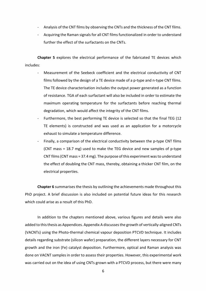
Figure 2-1. The number of Publications per year in the field of thermoelectricity between 1990
and 2016. Reproduced from the Web of Science 2018. ......................................................... 8
Figure 2-2. Schematic diagrams showing TE device configurations: (a) n-type TE elements
connected electrically and thermally in parallel, (b) n-type TE elements connected
electrically in series at opposite ends and thermally in parallel. .......................................... 10
Figure 2-3. A typical thermoelectric module showing the flow of charge carriers for both power
generation and cooling. Both electrons and holes diffuse from the hot end to the cold end.
Reproduced from [9]. ............................................................................................................ 11
Figure 2-4. Set up diagrams for: (a) Seebeck effect, (b) Peltier effect. ......................................... 12
Figure 2-5. Schematic diagrams for, (a) thermoelectric generator, (b) thermoelectric refrigerator
............................................................................................................................................... 13
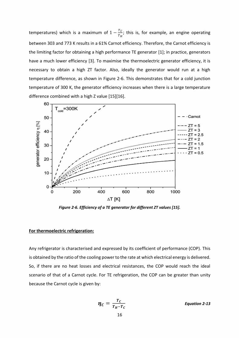
Figure 2-6. Efficiency of a TE generator for different ZT values [15]. ............................................ 16
Figure 2-7. Dependence on of electrical conductivity, Seebeck coefficient and power factor on
concentration of free carriers [16]. ....................................................................................... 19
Figure 2-8. Fermi distribution function plotted against E-EfkT [1]. .............................................. 21
Figure 2-9. Energy band diagram showing the valence and conduction bands separated by the
Fermi level. ............................................................................................................................ 21
Figure 2-10. Schematic diagram of energy states for different solids: (a) insulator, (b) intrinsic
semiconductor, (c) n-type semiconductor, (d) p-type semiconductor. ................................ 22
Figure 2-11. Crystallographic structure of Bi2Te3 by the stacking of cubes along the [111]
direction [22]. ........................................................................................................................ 23
Figure 2-12. Overview of developed thermoelectric materials and their ZT values [12][15]. ...... 26
Figure 2-13. Schematic diagram for the density of states in bulk materials in 3D, 2D, 1D and 0D
dimensionalities [30]. ............................................................................................................ 27
Figure 2-14. Schematic diagram highlighting the electronic density of states (DOS) for a
semiconducting SWCNT. The sharp peaks represent the Van Hove Singularities (VHS)
whereas the arrows show the energy difference between the sub bands [31]. .................. 29
Figure 2-15. (a) Schematic diagram of a plane graphene sheet which is rolled up to form a
carbon nanotube. (b) Atomic structure of an armchair. (c) atomic structure of a zig-zag
nanotube [36]. ....................................................................................................................... 30
Figure 2-16. Schematic diagram of the laser ablation method. A graphitic target mixed with a
catalyst is hit by a high beam laser resulting in CNTs which are deposited on a collector
[39]. ........................................................................................................................................ 31
Figure 2-17. Schematic for Arc-Discharge setup showing two electrodes where a high current is
passed through [45]. .............................................................................................................. 32
xi
Figure 2-18. CNT growth mechanism in CVD systems. It show the carbon molecules diffusing
around the metallic catalyst island which is the precursor of the CNT yield [50]. ............... 33
Figure 2-19. Schematic diagram for the CVD process for CNT synthesis. A hydrocarbon source
interacts with a catalyst inside the reactor chamber with the help of a plasma or a thermal
source like infrared lamps. The gases flow is controlled by a pressure gauge [51]. ............. 33
Figure 2-20. Schematic diagram showing the different mechanisms for the bonding of
surfactants on the SWCNT surface: (a) Surfactant micelles encapsulating a SWCNT, (b)
shows hemi-micellar absorption on the SWCNT, (c) Random formation/absorption of
surfactant molecules on SWCNT [62]. ................................................................................... 37
Figure 2-21. Graph shows the critical micelle concentration point (CMC) [66]. ........................... 39
Figure 2-22. Energy flow in internal combustion engines [4]. ....................................................... 46
Figure 2-23. Schematic diagram of a STEG system made with thermoelectric elements (p-type
and n-type semiconductors) and flat a panel on top which acts as a solar absorber (thermal
concentrator) [90]. ................................................................................................................ 48
Figure 3-1. Schematics of Van der Pauw configurations for sheet resistance showing the
different combinations [104]. ................................................................................................ 53
Figure 3-2. (a) Schematic diagram for Van der Pauw measurement sample holder, (b)
measurement rig where sample is placed on top of the black square holder and the four
external pin connectors are used to make good electrical contact [104]. ............................ 54
Figure 3-3. Metal contacts configuration for the TLM method, different spacings are used
between the metal strips for accurate measurements [107]. .............................................. 55
Figure 3-4. Typical graph of resistance showing the TLM method for various contact separations.
The data from the graph determines: TL = transfer length, RC = contact resistance, RS =
sheet resistance [107]. .......................................................................................................... 56
Figure 3-5. Calibration of the TLM method by measuring the resistivity of palladium showing two
different thicknesses. ............................................................................................................ 56
Figure 3-6. (a) Previous electrical probe used for the old setup. The benefit from using it was the
ability to lower the probe using the right hand knob. This allows to carefully control the
pressure put on the CNT sample, (b) Image showing spring loaded probes manually
controlled to prevent damage to the CNT films if they are in direct contact. ...................... 58
Figure 3-7. (a) Schematic diagram showing the components used for the Seebeck measurement
of the new setup, (b) measurement rig includes a vacuum chamber and multiple crocodile
clips to be connected for powering up the platinum resistors, as well as voltage Mueller
clips for recording potential differences across the CNT samples, plus thermocouples for
temperature recording, (c) example of CNT samples placed on a glass slide for better
handling where copper tapes and silver epoxy are used to electrically and thermally
connect the CNT samples. ..................................................................................................... 60
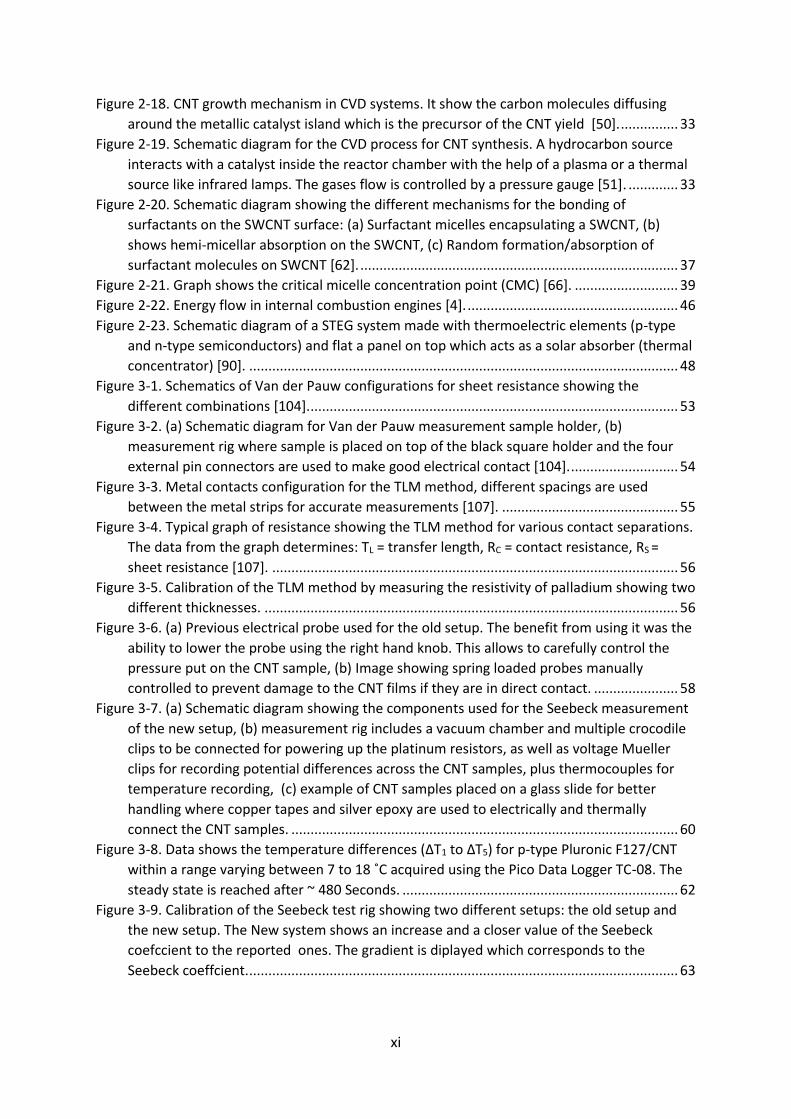
Figure 3-8. Data shows the temperature differences (ΔT1 to ΔT5) for p-type Pluronic F127/CNT
within a range varying between 7 to 18 ˚C acquired using the Pico Data Logger TC-08. The
steady state is reached after ~ 480 Seconds. ........................................................................ 62
Figure 3-9. Calibration of the Seebeck test rig showing two different setups: the old setup and
the new setup. The New system shows an increase and a closer value of the Seebeck
coefccient to the reported ones. The gradient is diplayed which corresponds to the
Seebeck coeffcient. ................................................................................................................ 63
xii
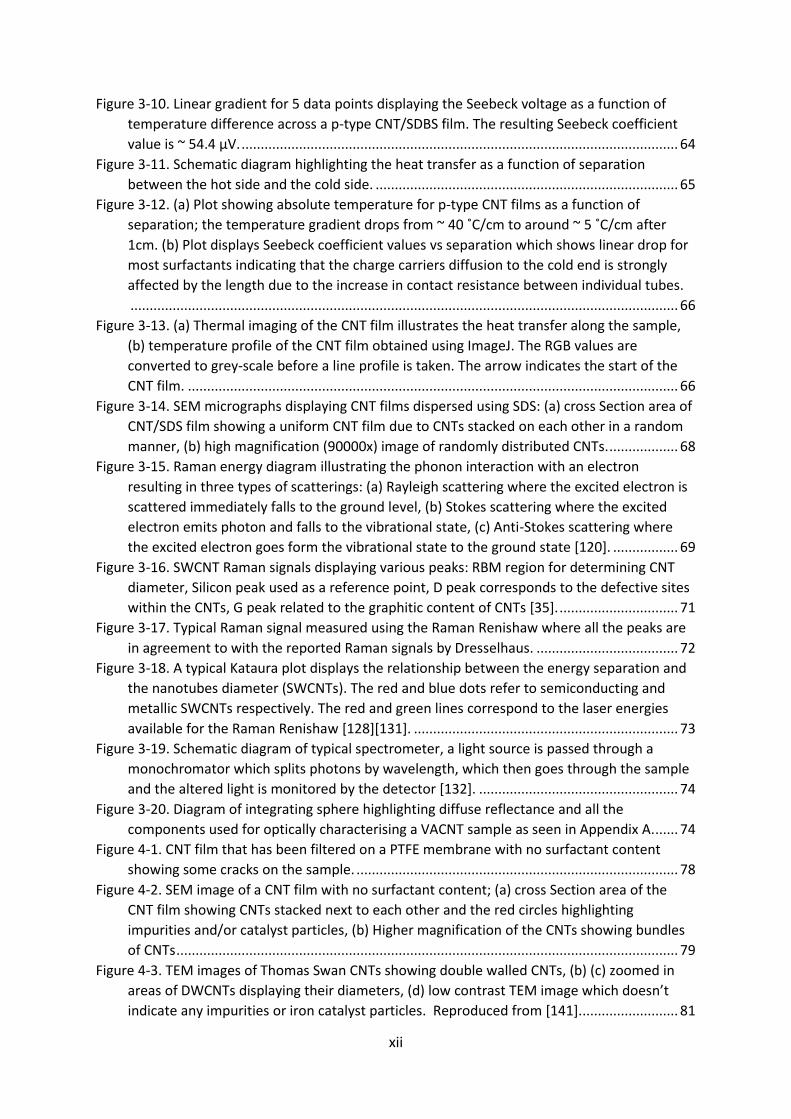
Figure 3-10. Linear gradient for 5 data points displaying the Seebeck voltage as a function of
temperature difference across a p-type CNT/SDBS film. The resulting Seebeck coefficient
value is ~ 54.4 µV. .................................................................................................................. 64
Figure 3-11. Schematic diagram highlighting the heat transfer as a function of separation
between the hot side and the cold side. ............................................................................... 65
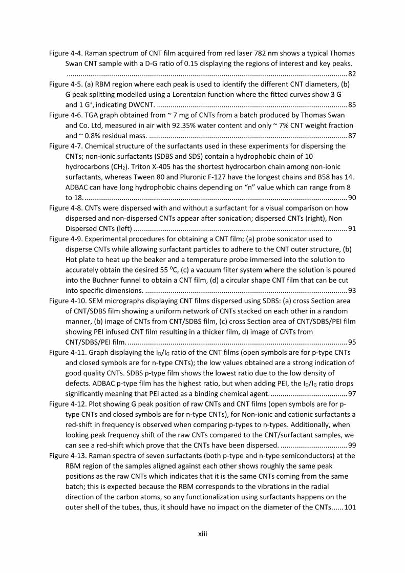
Figure 3-12. (a) Plot showing absolute temperature for p-type CNT films as a function of
separation; the temperature gradient drops from ~ 40 ˚C/cm to around ~ 5 ˚C/cm after
1cm. (b) Plot displays Seebeck coefficient values vs separation which shows linear drop for
most surfactants indicating that the charge carriers diffusion to the cold end is strongly
affected by the length due to the increase in contact resistance between individual tubes.
............................................................................................................................................... 66
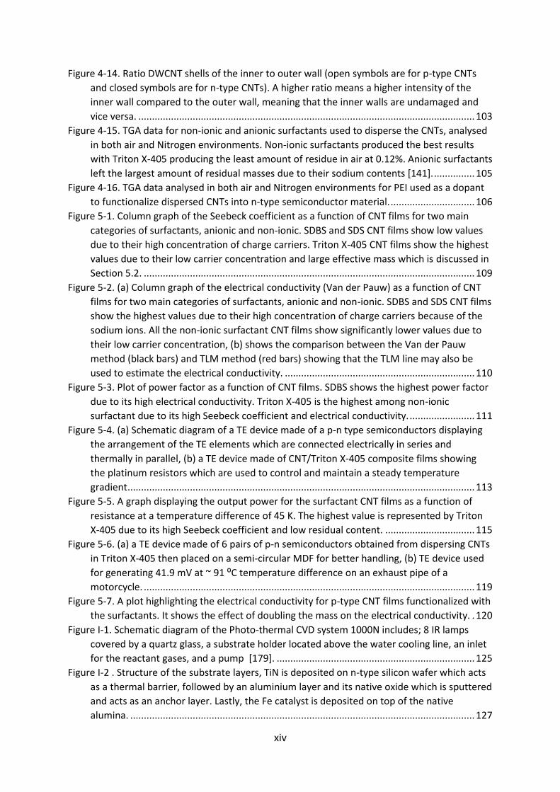
Figure 3-13. (a) Thermal imaging of the CNT film illustrates the heat transfer along the sample,
(b) temperature profile of the CNT film obtained using ImageJ. The RGB values are
converted to grey-scale before a line profile is taken. The arrow indicates the start of the
CNT film. ................................................................................................................................ 66
Figure 3-14. SEM micrographs displaying CNT films dispersed using SDS: (a) cross Section area of
CNT/SDS film showing a uniform CNT film due to CNTs stacked on each other in a random
manner, (b) high magnification (90000x) image of randomly distributed CNTs. .................. 68
Figure 3-15. Raman energy diagram illustrating the phonon interaction with an electron
resulting in three types of scatterings: (a) Rayleigh scattering where the excited electron is
scattered immediately falls to the ground level, (b) Stokes scattering where the excited
electron emits photon and falls to the vibrational state, (c) Anti-Stokes scattering where
the excited electron goes form the vibrational state to the ground state [120]. ................. 69
Figure 3-16. SWCNT Raman signals displaying various peaks: RBM region for determining CNT
diameter, Silicon peak used as a reference point, D peak corresponds to the defective sites
within the CNTs, G peak related to the graphitic content of CNTs [35]. ............................... 71
Figure 3-17. Typical Raman signal measured using the Raman Renishaw where all the peaks are
in agreement to with the reported Raman signals by Dresselhaus. ..................................... 72
Figure 3-18. A typical Kataura plot displays the relationship between the energy separation and
the nanotubes diameter (SWCNTs). The red and blue dots refer to semiconducting and
metallic SWCNTs respectively. The red and green lines correspond to the laser energies
available for the Raman Renishaw [128][131]. ..................................................................... 73
Figure 3-19. Schematic diagram of typical spectrometer, a light source is passed through a
monochromator which splits photons by wavelength, which then goes through the sample
and the altered light is monitored by the detector [132]. .................................................... 74
Figure 3-20. Diagram of integrating sphere highlighting diffuse reflectance and all the
components used for optically characterising a VACNT sample as seen in Appendix A. ...... 74
Figure 4-1. CNT film that has been filtered on a PTFE membrane with no surfactant content
showing some cracks on the sample. .................................................................................... 78
Figure 4-2. SEM image of a CNT film with no surfactant content; (a) cross Section area of the
CNT film showing CNTs stacked next to each other and the red circles highlighting
impurities and/or catalyst particles, (b) Higher magnification of the CNTs showing bundles
of CNTs ................................................................................................................................... 79
Figure 4-3. TEM images of Thomas Swan CNTs showing double walled CNTs, (b) (c) zoomed in
areas of DWCNTs displaying their diameters, (d) low contrast TEM image which doesn’t
indicate any impurities or iron catalyst particles. Reproduced from [141].......................... 81
xiii
Figure 4-4. Raman spectrum of CNT film acquired from red laser 782 nm shows a typical Thomas
Swan CNT sample with a D-G ratio of 0.15 displaying the regions of interest and key peaks.
............................................................................................................................................... 82
Figure 4-5. (a) RBM region where each peak is used to identify the different CNT diameters, (b)
G peak splitting modelled using a Lorentzian function where the fitted curves show 3 G-
and 1 G+, indicating DWCNT. ................................................................................................. 85
Figure 4-6. TGA graph obtained from ~ 7 mg of CNTs from a batch produced by Thomas Swan
and Co. Ltd, measured in air with 92.35% water content and only ~ 7% CNT weight fraction
and ~ 0.8% residual mass. ..................................................................................................... 87
Figure 4-7. Chemical structure of the surfactants used in these experiments for dispersing the
CNTs; non-ionic surfactants (SDBS and SDS) contain a hydrophobic chain of 10
hydrocarbons (CH2). Triton X-405 has the shortest hydrocarbon chain among non-ionic
surfactants, whereas Tween 80 and Pluronic F-127 have the longest chains and B58 has 14.
ADBAC can have long hydrophobic chains depending on “n” value which can range from 8
to 18. ...................................................................................................................................... 90
Figure 4-8. CNTs were dispersed with and without a surfactant for a visual comparison on how
dispersed and non-dispersed CNTs appear after sonication; dispersed CNTs (right), Non
Dispersed CNTs (left) ............................................................................................................. 91
Figure 4-9. Experimental procedures for obtaining a CNT film; (a) probe sonicator used to
disperse CNTs while allowing surfactant particles to adhere to the CNT outer structure, (b)
Hot plate to heat up the beaker and a temperature probe immersed into the solution to
accurately obtain the desired 55 ⁰C, (c) a vacuum filter system where the solution is poured
into the Buchner funnel to obtain a CNT film, (d) a circular shape CNT film that can be cut
into specific dimensions. ....................................................................................................... 93
Figure 4-10. SEM micrographs displaying CNT films dispersed using SDBS: (a) cross Section area
of CNT/SDBS film showing a uniform network of CNTs stacked on each other in a random
manner, (b) image of CNTs from CNT/SDBS film, (c) cross Section area of CNT/SDBS/PEI film
showing PEI infused CNT film resulting in a thicker film, d) image of CNTs from
CNT/SDBS/PEI film. ................................................................................................................ 95
Figure 4-11. Graph displaying the ID/IG ratio of the CNT films (open symbols are for p-type CNTs
and closed symbols are for n-type CNTs); the low values obtained are a strong indication of
good quality CNTs. SDBS p-type film shows the lowest ratio due to the low density of
defects. ADBAC p-type film has the highest ratio, but when adding PEI, the ID/IG ratio drops
significantly meaning that PEI acted as a binding chemical agent. ....................................... 97
Figure 4-12. Plot showing G peak position of raw CNTs and CNT films (open symbols are for p-
type CNTs and closed symbols are for n-type CNTs), for Non-ionic and cationic surfactants a
red-shift in frequency is observed when comparing p-types to n-types. Additionally, when
looking peak frequency shift of the raw CNTs compared to the CNT/surfactant samples, we
can see a red-shift which prove that the CNTs have been dispersed. .................................. 99
Figure 4-13. Raman spectra of seven surfactants (both p-type and n-type semiconductors) at the
RBM region of the samples aligned against each other shows roughly the same peak
positions as the raw CNTs which indicates that it is the same CNTs coming from the same
batch; this is expected because the RBM corresponds to the vibrations in the radial
direction of the carbon atoms, so any functionalization using surfactants happens on the
outer shell of the tubes, thus, it should have no impact on the diameter of the CNTs. ..... 101
xiv
Figure 4-14. Ratio DWCNT shells of the inner to outer wall (open symbols are for p-type CNTs
and closed symbols are for n-type CNTs). A higher ratio means a higher intensity of the
inner wall compared to the outer wall, meaning that the inner walls are undamaged and
vice versa. ............................................................................................................................ 103
Figure 4-15. TGA data for non-ionic and anionic surfactants used to disperse the CNTs, analysed
in both air and Nitrogen environments. Non-ionic surfactants produced the best results
with Triton X-405 producing the least amount of residue in air at 0.12%. Anionic surfactants
left the largest amount of residual masses due to their sodium contents [141]. ............... 105
Figure 4-16. TGA data analysed in both air and Nitrogen environments for PEI used as a dopant
to functionalize dispersed CNTs into n-type semiconductor material. ............................... 106
Figure 5-1. Column graph of the Seebeck coefficient as a function of CNT films for two main
categories of surfactants, anionic and non-ionic. SDBS and SDS CNT films show low values
due to their high concentration of charge carriers. Triton X-405 CNT films show the highest
values due to their low carrier concentration and large effective mass which is discussed in
Section 5.2. .......................................................................................................................... 109
Figure 5-2. (a) Column graph of the electrical conductivity (Van der Pauw) as a function of CNT
films for two main categories of surfactants, anionic and non-ionic. SDBS and SDS CNT films
show the highest values due to their high concentration of charge carriers because of the
sodium ions. All the non-ionic surfactant CNT films show significantly lower values due to
their low carrier concentration, (b) shows the comparison between the Van der Pauw
method (black bars) and TLM method (red bars) showing that the TLM line may also be
used to estimate the electrical conductivity. ...................................................................... 110
Figure 5-3. Plot of power factor as a function of CNT films. SDBS shows the highest power factor
due to its high electrical conductivity. Triton X-405 is the highest among non-ionic
surfactant due to its high Seebeck coefficient and electrical conductivity. ........................ 111
Figure 5-4. (a) Schematic diagram of a TE device made of a p-n type semiconductors displaying
the arrangement of the TE elements which are connected electrically in series and
thermally in parallel, (b) a TE device made of CNT/Triton X-405 composite films showing
the platinum resistors which are used to control and maintain a steady temperature
gradient ................................................................................................................................ 113
Figure 5-5. A graph displaying the output power for the surfactant CNT films as a function of
resistance at a temperature difference of 45 K. The highest value is represented by Triton
X-405 due to its high Seebeck coefficient and low residual content. ................................. 115
Figure 5-6. (a) a TE device made of 6 pairs of p-n semiconductors obtained from dispersing CNTs
in Triton X-405 then placed on a semi-circular MDF for better handling, (b) TE device used
for generating 41.9 mV at ~ 91 ⁰C temperature difference on an exhaust pipe of a
motorcycle. .......................................................................................................................... 119
Figure 5-7. A plot highlighting the electrical conductivity for p-type CNT films functionalized with
the surfactants. It shows the effect of doubling the mass on the electrical conductivity. . 120
Figure I-1. Schematic diagram of the Photo-thermal CVD system 1000N includes; 8 IR lamps
covered by a quartz glass, a substrate holder located above the water cooling line, an inlet
for the reactant gases, and a pump [179]. ......................................................................... 125
Figure I-2 . Structure of the substrate layers, TiN is deposited on n-type silicon wafer which acts
as a thermal barrier, followed by an aluminium layer and its native oxide which is sputtered
and acts as an anchor layer. Lastly, the Fe catalyst is deposited on top of the native
alumina. ............................................................................................................................... 127
xv
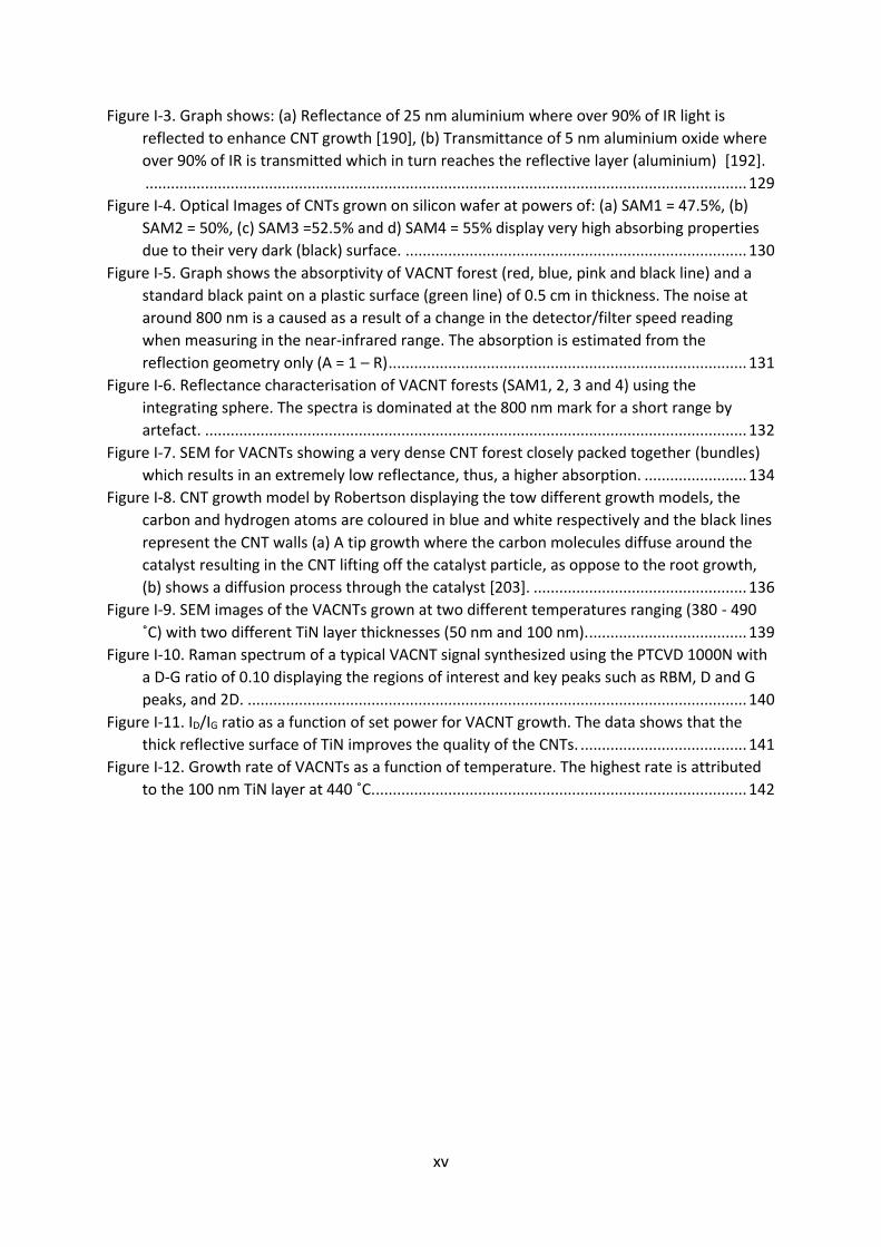
Figure I-3. Graph shows: (a) Reflectance of 25 nm aluminium where over 90% of IR light is
reflected to enhance CNT growth [190], (b) Transmittance of 5 nm aluminium oxide where
over 90% of IR is transmitted which in turn reaches the reflective layer (aluminium) [192].
............................................................................................................................................. 129
Figure I-4. Optical Images of CNTs grown on silicon wafer at powers of: (a) SAM1 = 47.5%, (b)
SAM2 = 50%, (c) SAM3 =52.5% and d) SAM4 = 55% display very high absorbing properties
due to their very dark (black) surface. ................................................................................ 130
Figure I-5. Graph shows the absorptivity of VACNT forest (red, blue, pink and black line) and a
standard black paint on a plastic surface (green line) of 0.5 cm in thickness. The noise at
around 800 nm is a caused as a result of a change in the detector/filter speed reading
when measuring in the near-infrared range. The absorption is estimated from the
reflection geometry only (A = 1 – R) .................................................................................... 131
Figure I-6. Reflectance characterisation of VACNT forests (SAM1, 2, 3 and 4) using the
integrating sphere. The spectra is dominated at the 800 nm mark for a short range by
artefact. ............................................................................................................................... 132
Figure I-7. SEM for VACNTs showing a very dense CNT forest closely packed together (bundles)
which results in an extremely low reflectance, thus, a higher absorption. ........................ 134
Figure I-8. CNT growth model by Robertson displaying the tow different growth models, the
carbon and hydrogen atoms are coloured in blue and white respectively and the black lines
represent the CNT walls (a) A tip growth where the carbon molecules diffuse around the
catalyst resulting in the CNT lifting off the catalyst particle, as oppose to the root growth,
(b) shows a diffusion process through the catalyst [203]. .................................................. 136
Figure I-9. SEM images of the VACNTs grown at two different temperatures ranging (380 - 490
˚C) with two different TiN layer thicknesses (50 nm and 100 nm). ..................................... 139
Figure I-10. Raman spectrum of a typical VACNT signal synthesized using the PTCVD 1000N with
a D-G ratio of 0.10 displaying the regions of interest and key peaks such as RBM, D and G
peaks, and 2D. ..................................................................................................................... 140
Figure I-11. ID/IG ratio as a function of set power for VACNT growth. The data shows that the
thick reflective surface of TiN improves the quality of the CNTs. ....................................... 141
Figure I-12. Growth rate of VACNTs as a function of temperature. The highest rate is attributed
to the 100 nm TiN layer at 440 ˚C. ....................................................................................... 142
xvi
List of Tables
Table 2-1. Equation parameters and their definition. ................................................................... 14
Table 2-2. Experimental results on bulk materials and their properties [22]................................ 25
Table 4-1. List of surfactants from three different categories depending on the polarity of their
hydrophilic ends: anionic with negative charge, cationic with positive charge and non-ionic
with no apparent charge. ...................................................................................................... 89
Table 4-2. CNT films thickness for both p-type and n-type semiconductors. N-type films are
thicker that the p-type samples due to the inclusion of PEI polymer which has a larger
molecular chain. .................................................................................................................... 95
Table 5-1. Comparison of triton X-405 performance against reported values by different groups.
............................................................................................................................................. 116
Table II-1. Raw data collected using the Van Der Pauw method for measuring the sheet
resistance and computing the electrical resistivity from the CNT film thicknesses. ........... 144

xvii
Abbreviations and Acronyms
α Seebeck coefficient
σ Electrical conductivity
ρ Electrical resistivity
κ Thermal conductivity
Al2O3 Aluminium oxide (Alumina)
Ar Argon
Bi2Te3 Bismuth Telluride
Brij 58 Polyethylene glycol hexadecyl ether
C2H2 Acetylene
CCVD Catalytic chemical vapour deposition
CMC Critical micelle concentration
CNT Carbon nanotube
CVD Chemical vapour deposition
DOS Density of states
dppp 1,3-bis(diphenylphosphino)propane
DW Deionized water
DWCNT Double wall carbon nanotube not defined in text
Fe Iron
H2 Hydrogen
ICE Internal Combustion Engines (defined at second use in text)
IR Infrared radiation
iTO In-plane transverse optical
iTOLA in-plane transverse optical branch + longitudinal acoustic
LA Longitudinal acoustic
LO Longitudinal optical
MDF Medium Density Fibreboard
m-SWCNT metallic single wall carbon nanotubes
MWCNT Multi wall carbon nanotube
N2 Nitrogen
xviii
Ni Nickel
NPL National Physical Laboratory
PECVD Plasma enhanced physical vapour deposition
PEI Polyethyleneimine
Pluronic F-127 Poloxamer
PTCVD Photo-thermal chemical vapour deposition
PVD Physical Vapor Deposition
RBM Radial breathing mode
SDBS Sodium dodecylbenzenesulfonate
SDS Sodium dodecyl sulfate
SEM Scanning electron microscopy
Si Silicon
SiC Silicon carbide
SiO2 Silicon dioxide
SiOx Silicon oxide(s)
s-SWCNT Semiconducting single wall carbon nanotube
STEG Solar thermoelectric generator
SWCNT Single wall carbon nanotube
TE Thermoelectric
TEG Thermoelectric generator
TEM Transmission electron microscopy
TGA Thermogravimetric analysis
TiN Titanium Nitride
TLM Transmission line measurement
tpp Triphenylphosphine
Triton X-405 Polyethylene glycol tert-octylphenyl ether
Tween 80 Polyethylene glycol sorbitan monooleate
VACNT Vertically aligned carbon nanotube
VHS Van Hove singularities
ZT Dimensionless Thermoelectric figure of merit
1
Introduction and objective
1.1 Background to the project
The increasing number of today’s world population and the decrease in fossil fuel
supplies have caused a significant increase in energy demand. This has prompted
Governments and research institutions to actively pursue alternative and clean energy
sources as well as ways to harvest wasted energy. One way to achieve this is by exploring the
use of advanced functional materials. However, there are many considerations to think of
such as: protecting the environment, efficient processing techniques, increased strength and
lightweight materials. An area of choice for modern applications would be thermoelectrics.
A thermoelectric (TE) device is an energy conversion device that uses the Seebeck
effect to produce a voltage difference when there is a temperature gradient across the device.
In an analogous manner, the Peltier effect is the generation of a heat flow (the presence of
heating or cooling) when current is passed through the device [1].
Due to high demand in energy converting materials, TE devices have drawn a broad attention
over the past few decades from various researchers, mainly because of their ability to convert
heat into electricity or vice versa. It is estimated that over 60% of the energy is lost worldwide
in the form of waste heat primarily [2]. This increase in demand has in turn raised the need
for a practical solution that can be used for various applications, which can be utilized in
different shaped components, hence the need for flexible materials.
In addition, TE devices are becoming increasingly important due to their potential applications
in energy harvesting from conventional heat-based processes. For example, conventional
thermal power stations and solar panels operate at an efficiency of 30-40%, which means that
the energy that is primarily lost by heat is estimated to account for 2/3 of the overall energy
produced [3]. Furthermore, internal combustion engines in both hydrocarbon and hybrid
electric vehicles utilize only 25% of the fuel’s energy, resulting in 75% wastage through heat
loss, mainly in the form of exhaust gas [4]. Thus, TE devices provide an important solution
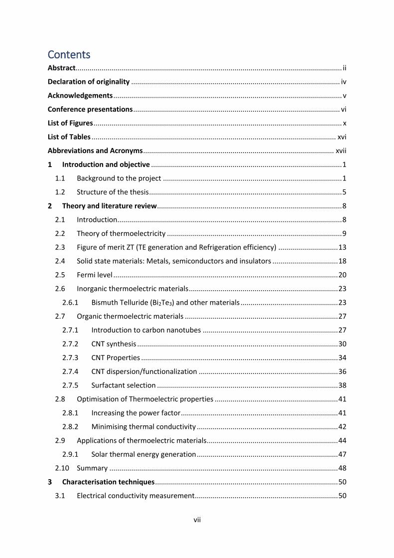
where waste heat can be harvested and then converted into electricity. Figure 1-1 describes
the energy lost in the form of waste heat where only a 1/3 is used.
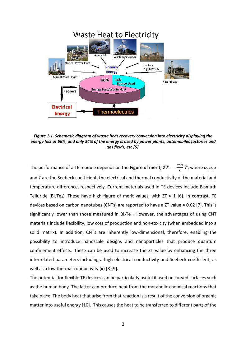
2
Figure 1-1. Schematic diagram of waste heat recovery conversion into electricity displaying the energy lost at 66%, and only 34% of the energy is used by power plants, automobiles factories and
gas fields, etc [5].
The performance of a TE module depends on the Figure of merit, 𝒁𝑻 = 𝜶𝟐𝝈
𝜿 𝑻, where α, σ, κ
and T are the Seebeck coefficient, the electrical and thermal conductivity of the material and
temperature difference, respectively. Current materials used in TE devices include Bismuth
Telluride (Bi2Te3). These have high figure of merit values, with ZT ≈ 1 [6]. In contrast, TE
devices based on carbon nanotubes (CNTs) are reported to have a ZT value ≈ 0.02 [7]. This is
significantly lower than those measured in Bi2Te3. However, the advantages of using CNT
materials include flexibility, low cost of production and non-toxicity (when embedded into a
solid matrix). In addition, CNTs are inherently low-dimensional, therefore, enabling the
possibility to introduce nanoscale designs and nanoparticles that produce quantum
confinement effects. These can be used to increase the ZT value by enhancing the three
interrelated parameters including a high electrical conductivity and Seebeck coefficient, as
well as a low thermal conductivity (κ) [8][9].
The potential for flexible TE devices can be particularly useful if used on curved surfaces such
as the human body. The latter can produce heat from the metabolic chemical reactions that
take place. The body heat that arise from that reaction is a result of the conversion of organic
matter into useful energy [10]. This causes the heat to be transferred to different parts of the
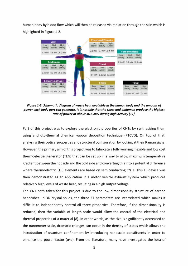
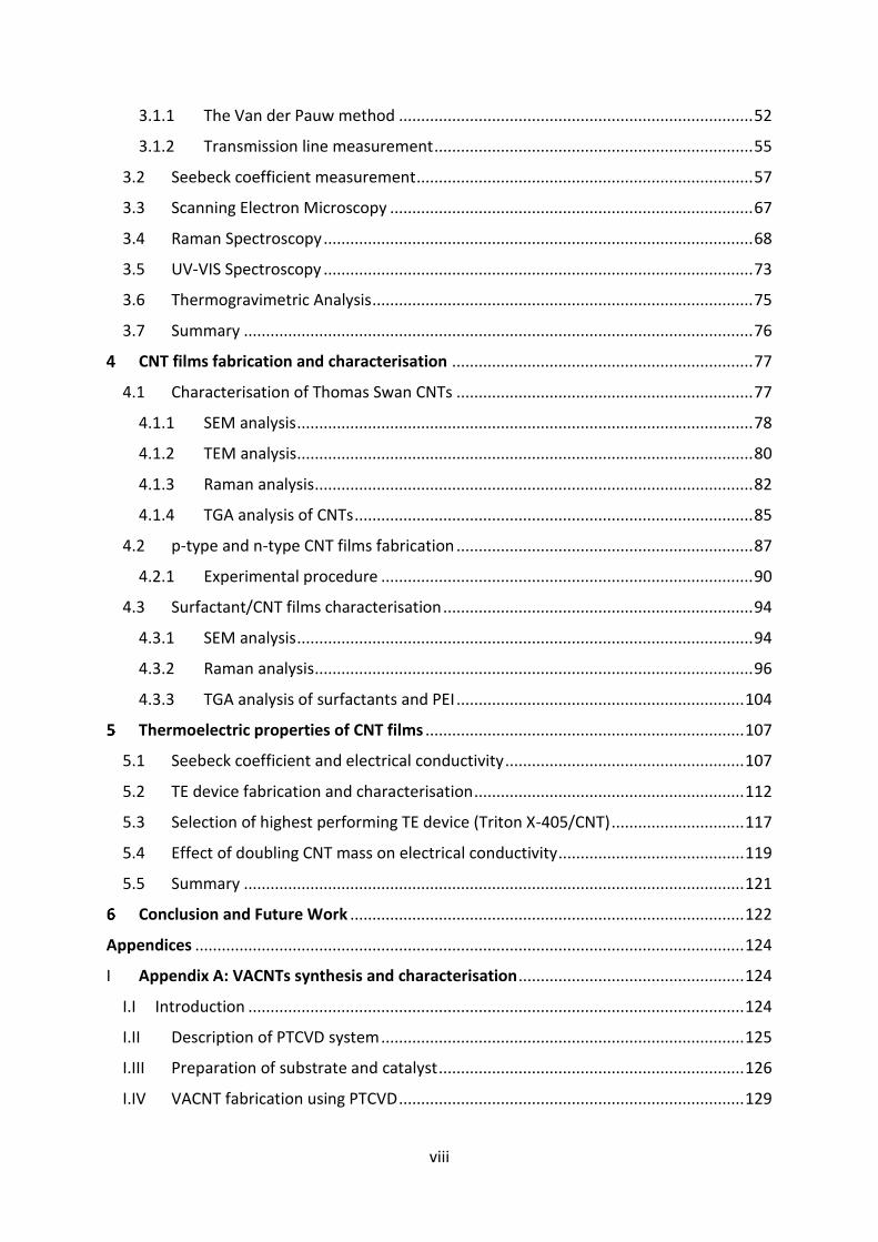
3
human body by blood flow which will then be released via radiation through the skin which is
highlighted in Figure 1-2.
Figure 1-2. Schematic diagram of waste heat available in the human body and the amount of power each body part can generate. It is notable that the chest and abdomen produce the highest
rate of power at about 36.6 mW during high activity [11].
Part of this project was to explore the electronic properties of CNTs by synthesising them
using a photo-thermal chemical vapour deposition technique (PTCVD). On top of that,
analysing their optical properties and structural configuration by looking at their Raman signal.
However, the primary aim of this project was to fabricate a fully working, flexible and low cost
thermoelectric generator (TEG) that can be set up in a way to allow maximum temperature
gradient between the hot side and the cold side and converting this into a potential difference
where thermoelectric (TE) elements are based on semiconducting CNTs. This TE device was
then demonstrated as an application in a motor vehicle exhaust system which produces
relatively high levels of waste heat, resulting in a high output voltage.
The CNT path taken for this project is due to the low-dimensionality structure of carbon
nanotubes. In 3D crystal solids, the three ZT parameters are interrelated which makes it
difficult to independently control all three properties. Therefore, if the dimensionality is
reduced, then the variable of length scale would allow the control of the electrical and
thermal properties of a material [8]. In other words, as the size is significantly decreased to
the nanometer scale, dramatic changes can occur in the density of states which allows the
introduction of quantum confinement by introducing nanoscale constituents in order to
enhance the power factor (α2σ). From the literature, many have investigated the idea of
4
decoupling the electronic Density of States (DOS) from the phonon DOS and thereby boosting
the ratio of the electrical conductivity to thermal conductivity (𝜎 𝜅⁄ ) [12][13]. So, if this can
be achieved on materials with a high Seebeck coefficient, then a high ZT can be significantly
higher. This concept of increasing the power factor will be discussed and analysed further in
Chapter 5.
Additionally, reducing the thermal conductivity is another requirement in order to obtain a
high ZT value which can be achieved by scattering of phonons; this will prevent a significant
amount of heat from flowing down across the TE elements where a temperature gradient
exists. However, characterising the thermal conductivity parameter was deemed to be a
complicated process. We attempted to measure the thermal conductivity by designing a
steady state rig adapted for thin films. However, this has proved very complicated by the fact
that the film is a random network of CNTs and the CNTs are very emissive (nearly perfect
blackbodies). Nevertheless, some very important design conclusions can be drawn from
examining the heat flux of the films (see Section 3.2). On the other hand, the power factor
proved to be a good measure of the efficiency of the films, so, we concentrated on measuring
it and finding ways to improve the power factor and investigate in detail the effect of
surfactants’ bonding onto the outer structure of CNTs and on the output power performance
of TE devices made of CNT films.
This work involves for the first time a systematic comparison between CNT films
manufactured using different surfactants, which lead to different electrical behaviour,
depending on the surfactant’s hydrophilic end polarity (positive, negative and neutral) and
direction of the dipole. A surfactant’s main advantage is to offer a non-covalent type of
functionalization, allowing the interaction between its hydrophobic part to bond with the
CNTs outer wall due to Van der Waal forces making them more soluble and less prone to
aggregate [14]. Furthermore, the data obtained from Raman spectroscopy revealed high
quality CNTs, with small variations in the D (defect) peak after functionalisation, as shown in
Section 4.3.2, which indicates that the surfactant-tube interaction is non-covalent.
Further to this, the dispersion efficiency was characterised by analysing the G (graphitic peak
Raman wavenumber position, where a shift was noticed for all surfactants/CNT composites
as a comparison to a non-functionalized CNT film. The shift in the G peak indicates that the
CNTs are coated with surfactant molecules and we also suggest that this is an indication of
the efficiency of dispersion.
5
Finally, by measuring the Seebeck coefficient and electrical conductivity, we show, for the
first time, that the optimum power factor is achieved via the non-ionic surfactant (no polarity)
Triton X-405; this gave the best performing TE device, generating ~ 1.5nW/K. In addition to
its neutral charge, Triton X-405 molecules have the shortest hydrophobic end compared to
the rest of the surfactants used for this project, which was correlated to a high Seebeck
coefficient and a relatively high electrical conductivity. This has resulted in the highest output
power which signifies that a short molecule reduces the tube-tube distance, thus, increasing
the conductivity.
1.2 Structure of the thesis
The thesis is organised as follow:
Chapter 2 discusses the theory behind thermoelectricity required to understand the
ZT parameters as well as the literature review which covers a description of the actual TE
devices that are available commercially most notably Bi2Te3. This is followed by an exploration
of the CNTs and their different synthesis techniques, their properties and how to functionalize
and disperse them. Furthermore, this chapter will also include an analysis on the categories
of surfactants used to functionalize CNTs.
Chapter 3 covers the characterisation techniques used for measuring the Seebeck
coefficient and electrical conductivity of the CNT films produced. In addition, SEM (scanning
electron microscopy), optical spectroscopy (for the as-grown CNTs using PTCVD), Raman
measurements and Thermogravimetric analysis (TGA) were all used for this project.
Chapter 4 explores the properties of Double wall CNTs (DWCNTs) synthesised by
Thomas Swan and the fabrication process of the CNT films. This chapter will include:
- Characterisation of non-functionalized (pristine) DWCNTs used for this project
which includes SEM, TEM and Raman analysis.
- Detail description of the functionalization and dispersion of the CNTs into p-type
(air exposed) and n-type (mixed with PEI) using 7 surfactants (Anionic, non-ionic
and cationic as well as the experimental process to obtain the CNT films after
vacuum filtration.
6
- Analysis of the CNT films by observing the CNTs and the thickness of the CNT films.
- Acquiring the Raman signals for all CNT films functionalized in order to understand
further the effect of the surfactants on the CNTs.
Chapter 5 explores the electrical performance of the fabricated TE devices which
includes:
- Measurement of the Seebeck coefficient and the electrical conductivity of CNT
films followed by the design of a TE device made of a p-type and n-type CNT films.
The TE device characterisation includes the output power generated as a function
of resistance. TGA of each surfactant will also be included in order to estimate the
maximum operating temperature for the surfactants before reaching thermal
degradation, which would affect the integrity of the CNT films.
- Furthermore, the best performing TE device is selected so that the final TEG (12
TE elements) is constructed and was used as an application for a motorcycle
exhaust to simulate a temperature difference.
- Finally, a comparison of the electrical conductivity between the p-type CNT films
(CNT mass = 18.7 mg) used to make the TEG device and new samples of p-type
CNT films (CNT mass = 37.4 mg). The purpose of this experiment was to understand
the effect of doubling the CNT mass, thereby, obtaining a thicker CNT film, on the
electrical properties.
Chapter 6 summarises the thesis by outlining the achievements made throughout this
PhD project. A brief discussion is also included on potential future ideas for this research
which could arise as a result of this PhD.
In addition to the chapters mentioned above, various figures and details were also
added to this thesis as Appendices. Appendix A discusses the growth of vertically-aligned CNTs
(VACNTs) using the Photo-thermal chemical vapour deposition PTCVD technique. It includes
details regarding substrate (silicon wafer) preparation, the different layers necessary for CNT
growth and the iron (Fe) catalyst deposition. Furthermore, optical and Raman analysis was
done on VACNT samples in order to assess their properties. However, this experimental work
was carried out on the idea of using CNTs grown with a PTCVD process, but there were many

7
challenges that have been faced which prevented this path to be followed, thus, commercial
CNTs (Thomas Swan) have been used instead. Therefore, some of the difficulties encountered
using this growth technique are discussed in the Appendix A.
8
Theory and literature review
2.1 Introduction
The concept of thermoelectricity was first discovered in 1821 by Thomas J. Seebeck
who first observed the behaviour of a needle of a compass that was deflected when in close
proximity to two joined metallic conductors [15]. The junction connecting the two materials
was exposed to various temperatures, therefore the degree of deflection away from the
vicinity of the joint was observed to be proportional to the temperature gradient. It was
believed that the reason for the needle’s movement was due to the electrical field created at
the junction between the conductors by the temperature difference. The opposite effect was
also discovered later on in 1834 by Jean C. A. Peltier: a current is applied to two conductors
which results in a (negative) temperature difference. Thus, heat is transferred from one point
to the other causing a cooling effect. Since then, research in the field of thermoelectricity has
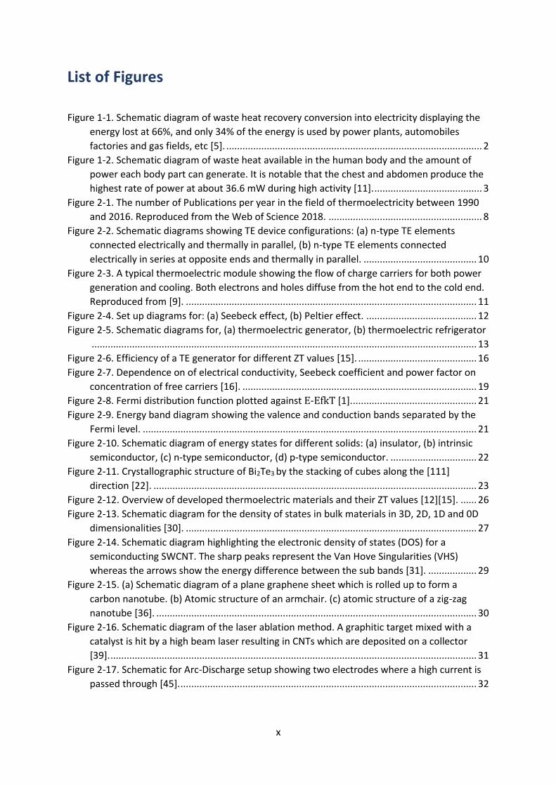
seen a significant increase. Figure 2-1 displays the number of publications from 1990 to 2016
which shows the significant worldwide adoption and activity in this area of physics by research
institutions.
Figure 2-1. The number of Publications per year in the field of thermoelectricity between 1990 and 2016. Reproduced from the Web of Science 2018.
1992 1995 1998 2001 2004 2007 2010 2013 2016
0
500
1000
1500
2000
2500
3000
Pu
blic
atio
ns
Year
9
2.2 Theory of thermoelectricity
The thermoelectric effect consists of heating the junction between two dissimilar
electrical conductors resulting in the production of an electromotive force. This phenomenon
arises due to the difference in the free movement of charge carriers (carrying charge and
heat) in metals and semiconductors. When a temperature difference exists between the
junction and the circuit-ends of the materials, the majority carriers (electrons for n-doped and
holes for p-doped) diffuse from the hot end to the cold end, where the charge carriers build
up, producing a voltage. This is known as the Seebeck effect, which is the basis of
thermoelectric power generation. Electrons and holes thermodynamically diffuse to the cold
end seeking thermal equilibrium, therefore, an electric field builds up. However, at higher
temperatures, the periodic collective excitations of a material’s atoms (phonons) will interact
with electrons and cause carrier scattering, thus, as the electron scattering increases, the
mobility decreases. In conclusion, it is ideal to operate at a relatively low average
temperature, but a high temperature gradient.
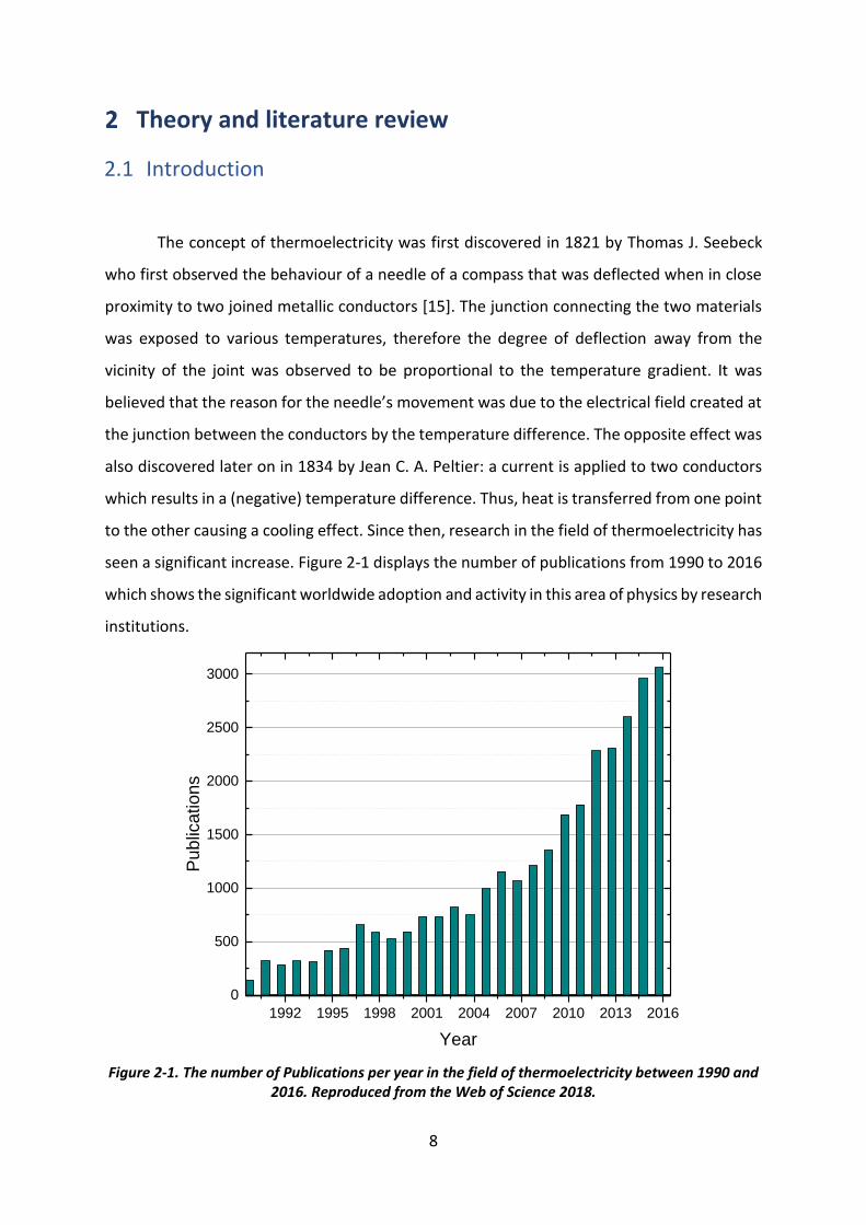
A thermoelectric device can have multiple arrangements, with the goal being to
increase the output voltage. As seen in Figure 2-2 (a), this configuration can consist of two
n-type TE elements electrically and thermally in parallel. The drawback in this design is the
generation of a low potential difference with high current. Another configuration can be
observed in Figure 2-2 (b) where two n-type TE elements are electrically connected in series
at opposite ends, and thermally in parallel. This arrangement presents a disadvantage in that,
it allows a larger heat transfer across the interconnect, thus, reducing the charge transfer
from the hot side to the cold side and the efficiency of the device.
Therefore, the solution to this problem is using n-type and p-type semiconductors in order to
form a thermocouple and increase the potential difference. Furthermore, if a thermocouple
is made of homogenous materials, then no electromotive force can be produced because the
Seebeck coefficient would be identical as seen in the following equation:
𝒅𝑬𝑨𝑩
𝒅𝑻= 𝜶𝑨 − 𝜶𝑩 Equation 2-1
10
Figure 2-2. Schematic diagrams showing TE device configurations: (a) n-type TE elements connected electrically and thermally in parallel, (b) n-type TE elements connected electrically in
series at opposite ends and thermally in parallel.
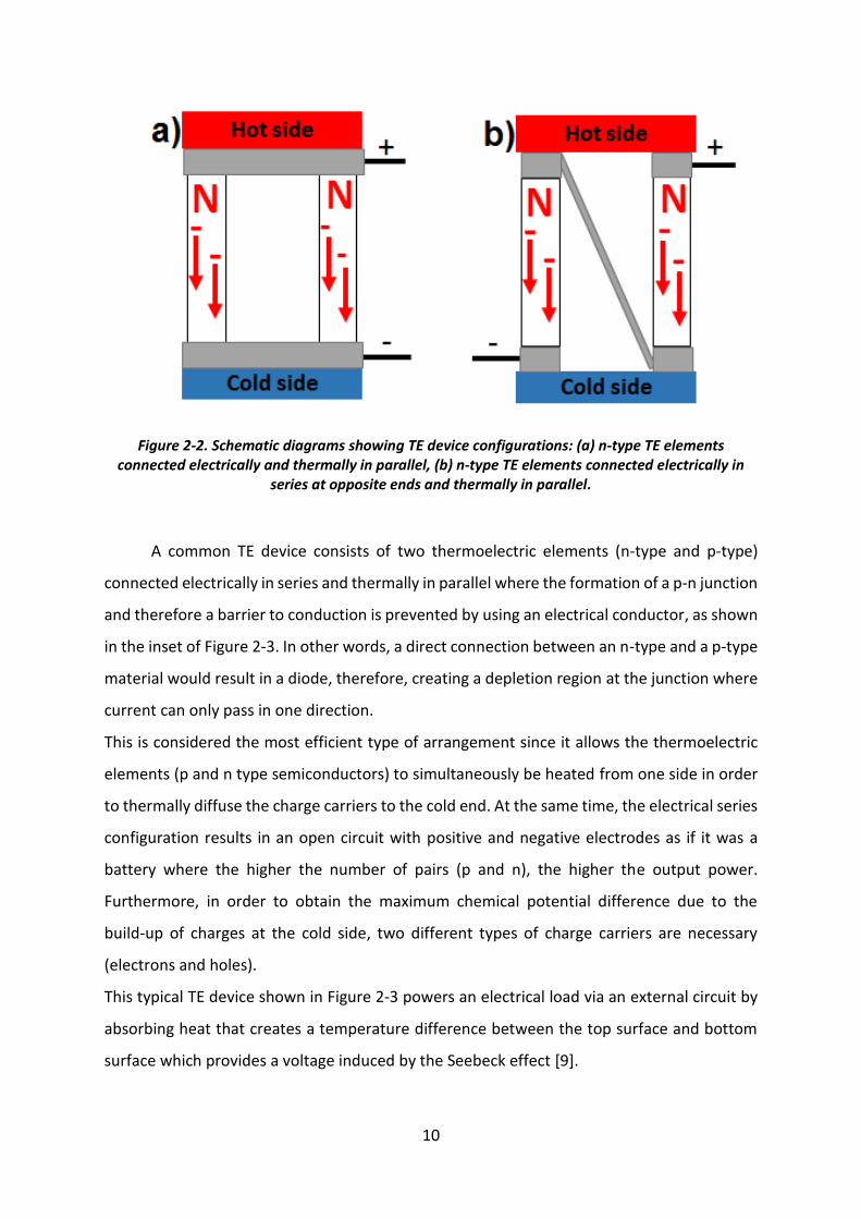
A common TE device consists of two thermoelectric elements (n-type and p-type)
connected electrically in series and thermally in parallel where the formation of a p-n junction
and therefore a barrier to conduction is prevented by using an electrical conductor, as shown
in the inset of Figure 2-3. In other words, a direct connection between an n-type and a p-type
material would result in a diode, therefore, creating a depletion region at the junction where
current can only pass in one direction.
This is considered the most efficient type of arrangement since it allows the thermoelectric
elements (p and n type semiconductors) to simultaneously be heated from one side in order
to thermally diffuse the charge carriers to the cold end. At the same time, the electrical series
configuration results in an open circuit with positive and negative electrodes as if it was a
battery where the higher the number of pairs (p and n), the higher the output power.
Furthermore, in order to obtain the maximum chemical potential difference due to the
build-up of charges at the cold side, two different types of charge carriers are necessary
(electrons and holes).
This typical TE device shown in Figure 2-3 powers an electrical load via an external circuit by
absorbing heat that creates a temperature difference between the top surface and bottom
surface which provides a voltage induced by the Seebeck effect [9].
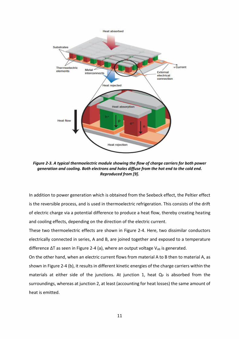
11
Figure 2-3. A typical thermoelectric module showing the flow of charge carriers for both power generation and cooling. Both electrons and holes diffuse from the hot end to the cold end.
Reproduced from [9].
In addition to power generation which is obtained from the Seebeck effect, the Peltier effect
is the reversible process, and is used in thermoelectric refrigeration. This consists of the drift
of electric charge via a potential difference to produce a heat flow, thereby creating heating
and cooling effects, depending on the direction of the electric current.
These two thermoelectric effects are shown in Figure 2-4. Here, two dissimilar conductors
electrically connected in series, A and B, are joined together and exposed to a temperature
difference ΔT as seen in Figure 2-4 (a), where an output voltage Vab is generated.
On the other hand, when an electric current flows from material A to B then to material A, as
shown in Figure 2-4 (b), it results in different kinetic energies of the charge carriers within the
materials at either side of the junctions. At junction 1, heat QP is absorbed from the
surroundings, whereas at junction 2, at least (accounting for heat losses) the same amount of
heat is emitted.
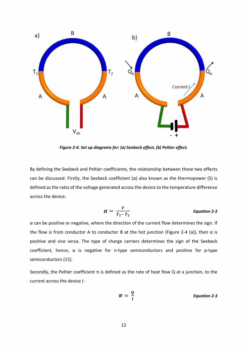
12
Figure 2-4. Set up diagrams for: (a) Seebeck effect, (b) Peltier effect.
By defining the Seebeck and Peltier coefficients, the relationship between these two effects
can be discussed. Firstly, the Seebeck coefficient (α) also known as the thermopower (S) is
defined as the ratio of the voltage generated across the device to the temperature difference
across the device:
𝜶 = 𝑽
𝑻𝟏− 𝑻𝟐 Equation 2-2
α can be positive or negative, where the direction of the current flow determines the sign. If
the flow is from conductor A to conductor B at the hot junction (Figure 2-4 (a)), then α is
positive and vice versa. The type of charge carriers determines the sign of the Seebeck
coefficient, hence, α is negative for n-type semiconductors and positive for p-type
semiconductors [15].
Secondly, the Peltier coefficient π is defined as the rate of heat flow Q at a junction, to the
current across the device I:
𝝅 = 𝑸
𝑰 Equation 2-3
13
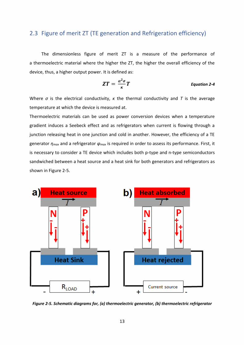
2.3 Figure of merit ZT (TE generation and Refrigeration efficiency)
The dimensionless figure of merit ZT is a measure of the performance of
a thermoelectric material where the higher the ZT, the higher the overall efficiency of the
device, thus, a higher output power. It is defined as:
𝒁𝑻 = 𝜶𝟐𝝈
𝜿𝑻 Equation 2-4
Where σ is the electrical conductivity, κ the thermal conductivity and T is the average
temperature at which the device is measured at.
Thermoelectric materials can be used as power conversion devices when a temperature
gradient induces a Seebeck effect and as refrigerators when current is flowing through a
junction releasing heat in one junction and cold in another. However, the efficiency of a TE
generator ηmax and a refrigerator φmax is required in order to assess its performance. First, it
is necessary to consider a TE device which includes both p-type and n-type semiconductors
sandwiched between a heat source and a heat sink for both generators and refrigerators as
shown in Figure 2-5.
Figure 2-5. Schematic diagrams for, (a) thermoelectric generator, (b) thermoelectric refrigerator

14
Additionally, before going through the derivation of the equations, let’s identify the different
parameters, as seen in the table below:
Table 2-1. Equation parameters and their definition.
Parameter Definition
ф Generator efficiency
COP coefficient of performance
I Current
R Material’s resistance
TH Heat source temperature
TC Heat sink temperature
�̅� Arithmetic temperature
κ Thermal conductance
Z Figure of merit
ηC Carnot cycle
γ ZT factor
αab Seebeck coefficient
ΔT Temperature difference
P Input power
For thermoelectric generation:
Since a TE converter is a heat engine, we first need to consider the converter as an ideal
generator during operation in which there are no heat losses by convection and conduction
through the surrounding medium as well as thermal radiation. Therefore, the efficiency is
defined as the ratio of the power delivered to an external load to the heat absorption at the
junction between two dissimilar materials a and b:
𝝓 = 𝒆𝒍𝒆𝒄𝒕𝒓𝒊𝒄𝒂𝒍 𝒑𝒐𝒘𝒆𝒓 𝒔𝒖𝒑𝒑𝒍𝒊𝒆𝒅 𝒕𝒐 𝒕𝒉𝒆 𝒍𝒐𝒂𝒅
𝒉𝒆𝒂𝒕 𝒆𝒏𝒆𝒓𝒈𝒚 𝒂𝒃𝒔𝒐𝒓𝒃𝒆𝒅 𝒂𝒕 𝒕𝒉𝒆 𝒉𝒐𝒕 𝒋𝒖𝒏𝒄𝒕𝒊𝒐𝒏 Equation 2-5
15
Assuming that the Seebeck coefficient, electrical conductivity and thermal conductivity are
constant and the contact resistances are negligible, then the efficiency can be expressed as:
𝝓 = 𝑰𝟐𝑹
𝜶𝒂𝒃𝑰𝑻𝑯= 𝜿(𝑻𝑯−𝑻𝑪)− 𝟏
𝟐𝑰𝟐𝑹
Equation 2-6
Efficiency is a function of the ratio of the load resistance to the sum of the thermoelectric
elements (arms) resistances, and at maximum output power, it is expressed as [16]:
𝝓𝒑 = 𝑻𝑯−𝑻𝑪
𝟑𝑻𝑯𝟐
+𝑻𝑪𝟐
+ 𝟒
𝒁
𝟏 Equation 2-7
Thus, the maximum efficiency is: 𝝓𝒎𝒂𝒙 = 𝜼𝑪𝜸 Equation 2-8
Where: 𝜼𝑪 = 𝑻𝑯−𝑻𝑪
𝑻𝑯 Equation 2-9
and 𝜸 = (√𝟏+𝐙�̅�−𝟏
√𝟏+𝐙�̅�+𝐓𝐡 𝐓𝐜⁄) Equation 2-10
Where the arithmetic temperature �̅� is given by:
�̅� = 𝑻𝑯 + 𝑻𝑪
𝟐 Equation 2-11
Therefore, the maximum TE generator efficiency is given by:
𝛈𝐦𝐚𝐱 = (𝐓𝐡− 𝐓𝐜
𝐓𝐡) (
√𝟏+𝐙�̅�−𝟏
√𝟏+𝐙�̅�+𝐓𝐡 𝐓𝐜⁄) Equation 2-12
The Carnot engine is an ideal thermodynamic generator which takes energy from a hot source
and converts some to energy and some is transferred to a cold source, reversibly, with no
losses, for which we can defined an ‘ideal’ Carnot efficiency. For a TE generator, the first ratio
of Equation 2-12 represents the Carnot efficiency (ideal heat engine, whose theoretical
maximum efficiency can be obtained when the heat engine is operating between two
16
temperatures) which is a maximum of 1 −𝑇𝐶
𝑇𝐻; this is, for example, an engine operating
between 303 and 773 K results in a 61% Carnot efficiency. Therefore, the Carnot efficiency is
the limiting factor for obtaining a high performance TE generator [1]; in practice, generators
have a much lower efficiency [3]. To maximise the thermoelectric generator efficiency, it is
necessary to obtain a high ZT factor. Also, ideally the generator would run at a high
temperature difference, as shown in Figure 2-6. This demonstrates that for a cold junction
temperature of 300 K, the generator efficiency increases when there is a large temperature
difference combined with a high Z value [15][16].
Figure 2-6. Efficiency of a TE generator for different ZT values [15].
For thermoelectric refrigeration:
Any refrigerator is characterised and expressed by its coefficient of performance (COP). This
is obtained by the ratio of the cooling power to the rate at which electrical energy is delivered.
So, if there are no heat losses and electrical resistances, the COP would reach the ideal
scenario of that of a Carnot cycle. For TE refrigeration, the COP can be greater than unity
because the Carnot cycle is given by:
𝜼𝑪 = 𝑻𝑪
𝑻𝑯−𝑻𝑪 Equation 2-13
17
Using the Kelvin relationship which relates the Peltier effect and the Seebeck effect at the
junction, it is given by:
𝜶𝒂𝒃 =𝝅𝒂𝒃
𝑻𝑪 Equation 2-14
𝝅𝒂𝒃𝑰 = 𝜶𝒂𝒃 (�̅� −∆𝑻
𝟐) 𝑰 Equation 2-15
The rate of absorption of heat from the source is expressed by:
𝑸𝒂𝒃 = 𝜶𝒂𝒃 𝑻𝑪 𝑰 − 𝟏
𝟐𝑰𝟐𝑹− 𝑲(𝑻𝑯 − 𝑻𝑪) Equation 2-16
With the input power given by:
𝑷 = 𝜶𝒂𝒃 ∆𝑻 𝑰 + 𝑰𝟐𝑹 Equation 2-17
So, a refrigerator energy efficiency which is measured by its COP which is defined as:
𝑪𝑶𝑷 = 𝑯𝒆𝒂𝒕 𝒂𝒃𝒔𝒐𝒓𝒃𝒆𝒅
𝑰𝒏𝒑𝒖𝒕 𝒑𝒐𝒘𝒆𝒓 Equation 2-18
𝑪𝑶𝑷 = 𝜶𝒂𝒃 𝑻𝑪 𝑰−
𝟏
𝟐𝑰𝟐𝑹− 𝑲(𝑻𝑯−𝑻𝑪)
𝜶𝒂𝒃 ∆𝑻 𝑰+𝑰𝟐𝑹 Equation 2-19
Then, the two current values of special interest are Iφ which gives the maximum cooling
power and satisfies the maximum COP condition can be expressed as follow [16]:
𝐼𝜙 = 𝛼𝑎𝑏(𝑇𝐻−𝑇𝐶)
√𝑅(1+𝑍𝑇)−1
Therefore, the maximum TE refrigerator efficiency is given by [17]:
𝛗𝐦𝐚𝐱 = (𝑻𝒄
𝑻𝒉− 𝑻𝒄) (
√𝟏+𝒁�̅�−𝑻𝒉 𝑻𝒄⁄
√𝟏+𝒁�̅�+𝟏) Equation 2-20
18
2.4 Solid state materials: Metals, semiconductors and insulators
After describing the efficiency of a TE device and its temperature dependency, it is
now important to understand the effect of the electrons and holes. Charge carrier
concentration influences the electrical conductivity of a material. The three parameters
relevant to thermoelectricity α, and in (Equation 2-4) are plotted as a function of electrons
and holes concentration [16] as shown in Figure 2-7. It demonstrates how the charge carrier
concentration influences the ZT parameter. The figure shows that the electrical conductivity
increases with increasing carrier concentration while at the same time, the Seebeck
coefficient decreases. This leads to an optimum power factor, which is only reached with
semiconducting materials due to their ideal carrier concentration, which is of the order of
1019 cm-3. In other words, semiconductors offer the best compromise between the Seebeck
coefficient, electrical conductivity and thermal conductivity which will maximise the efficiency
ZT of TE devices. It is noted that although the Seebeck coefficient may peak for a particular
doping level, this may not coincide with peak ZT parameter, since the doping level affects also
the thermal and electrical conductivities (higher levels increase these). These are taken into
account only for the ZT value, not the Seebeck coefficient.
Furthermore, it is known that for most electrical conductors the transport of heat (thermal
conductivity, ) is performed also by the drift of charge carriers (both electrons and holes)
whilst phonon heat transfer accounts for a more significant contribution to the thermal
conductivity of nearly 2/3. From Figure 2-7, it is observed that the electronic contribution
(representing 1/3 of the total heat conducted) increases as a function of the carrier
concentration. This further emphasizes that the optimum ZT value can be obtained with a
semiconductor material with intermediate values of carrier densities which is located at the
crossover between a metal and a semiconductor [18]. This is attributed to a large effective
mass (high Seebeck coefficient) but a low carrier mobility (low electrical conductivity); this
balance between the electrical parameters can be beneficial since a low electrical
conductivity means a low thermal conductivity, thus, a larger temperature gradient across
the material is maintained. In addition, semiconductors can be heavily doped with carrier
densities ranging from 1019 to 1021 cm-3 which would allow a higher ZT value to be obtained.
This point can be further emphasized by observing the high Seebeck coefficient and the low
electrical conductivity at low carrier concentration. It is noticed that an extremely high
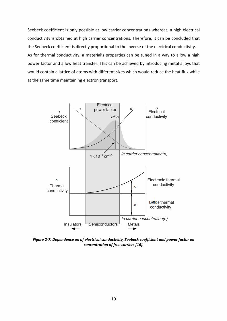
19
Seebeck coefficient is only possible at low carrier concentrations whereas, a high electrical
conductivity is obtained at high carrier concentrations. Therefore, it can be concluded that
the Seebeck coefficient is directly proportional to the inverse of the electrical conductivity.
As for thermal conductivity, a material’s properties can be tuned in a way to allow a high
power factor and a low heat transfer. This can be achieved by introducing metal alloys that
would contain a lattice of atoms with different sizes which would reduce the heat flux while
at the same time maintaining electron transport.
Figure 2-7. Dependence on of electrical conductivity, Seebeck coefficient and power factor on concentration of free carriers [16].
20
2.5 Fermi level
In crystalline metals and semiconductors, the transport of charge and heat takes place
by carrier drift and carrier diffusion. The thermal vibrations of the atoms in the crystal known
as phonons, also carry heat [1]. However, for materials with a high density of free charge
carriers, contributions from electronic effects are significantly stronger than those from
phonon wave propagation.
Drude and Lorentz proposed the idea of electrical conduction by electrons. But this was not
fully understood until the idea of the electrons interacting with the periodic potential in a
crystal lattice was introduced. This interaction causes the electrons energy to lie in discrete
bands separated by an energy gap [1].
To further understand the transport properties in a solid, it is vital to comprehend the Fermi
level. The Fermi distribution function given by equation 2-21 describes the distribution of
Fermions (such as electrons) over states of energy (E) in a system.
𝒇(𝑬) =𝟏
[𝒆(𝑬−𝑬𝒇𝒌𝑻
)+𝟏]
Equation 2-21
Where:
kB is Boltzmann's constant
T is the absolute temperature
E is the energy of the single-particle state i
EF is the total chemical potential
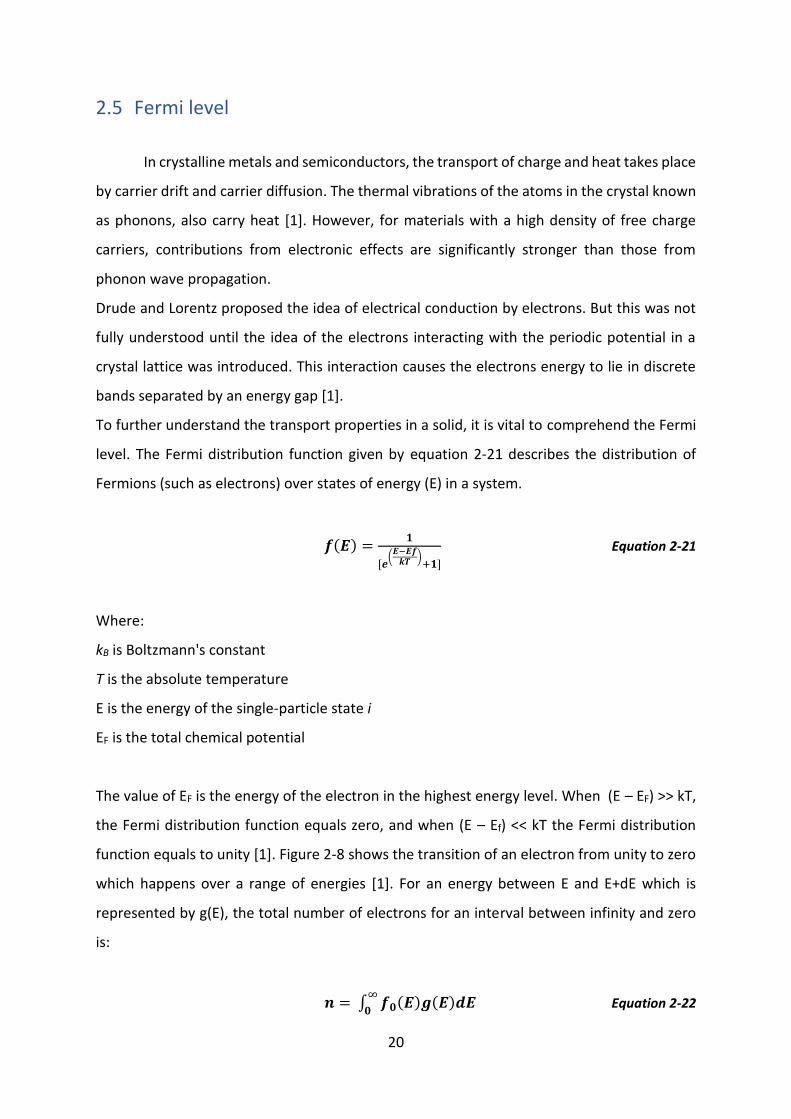
The value of EF is the energy of the electron in the highest energy level. When (E – EF) >> kT,
the Fermi distribution function equals zero, and when (E – Ef) << kT the Fermi distribution
function equals to unity [1]. Figure 2-8 shows the transition of an electron from unity to zero
which happens over a range of energies [1]. For an energy between E and E+dE which is
represented by g(E), the total number of electrons for an interval between infinity and zero
is:
𝒏 = ∫ 𝒇𝟎(𝑬)𝒈(𝑬)𝒅𝑬∞
𝟎 Equation 2-22
21
Figure 2-8. Fermi distribution function plotted against (𝑬−𝑬𝒇
𝒌𝑻) [1].
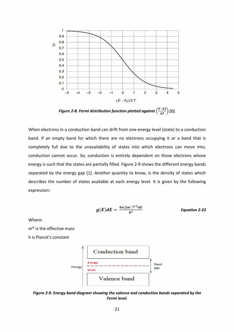
When electrons in a conduction band can drift from one energy level (state) to a conduction
band. If an empty band for which there are no electrons occupying it or a band that is
completely full due to the unavailability of states into which electrons can move into,
conduction cannot occur. So, conduction is entirely dependent on those electrons whose
energy is such that the states are partially filled. Figure 2-9 shows the different energy bands
separated by the energy gap [1]. Another quantity to know, is the density of states which
describes the number of states available at each energy level. It is given by the following
expression:
𝒈(𝑬)𝒅𝑬 = 𝟒𝝅(𝟐𝒎∗)𝟑 𝟐⁄ 𝒅𝑬
𝒉𝟑 Equation 2-23
Where:
m* is the effective mass
h is Planck’s constant
Figure 2-9. Energy band diagram showing the valence and conduction bands separated by the Fermi level.
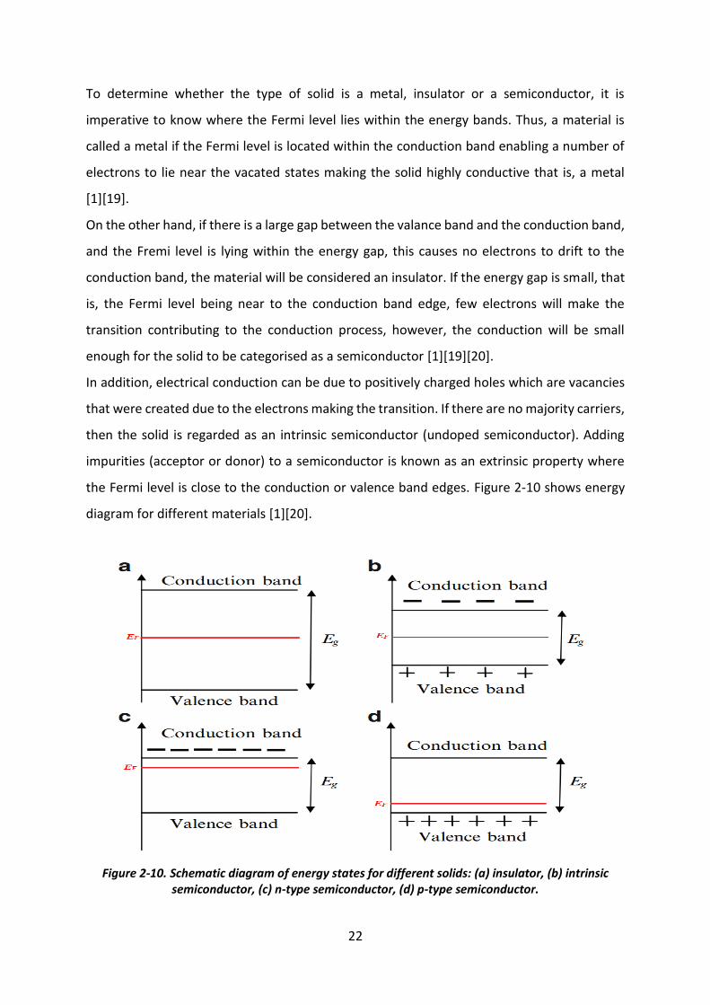
22
To determine whether the type of solid is a metal, insulator or a semiconductor, it is
imperative to know where the Fermi level lies within the energy bands. Thus, a material is
called a metal if the Fermi level is located within the conduction band enabling a number of
electrons to lie near the vacated states making the solid highly conductive that is, a metal
[1][19].
On the other hand, if there is a large gap between the valance band and the conduction band,
and the Fremi level is lying within the energy gap, this causes no electrons to drift to the
conduction band, the material will be considered an insulator. If the energy gap is small, that
is, the Fermi level being near to the conduction band edge, few electrons will make the
transition contributing to the conduction process, however, the conduction will be small
enough for the solid to be categorised as a semiconductor [1][19][20].
In addition, electrical conduction can be due to positively charged holes which are vacancies
that were created due to the electrons making the transition. If there are no majority carriers,
then the solid is regarded as an intrinsic semiconductor (undoped semiconductor). Adding
impurities (acceptor or donor) to a semiconductor is known as an extrinsic property where
the Fermi level is close to the conduction or valence band edges. Figure 2-10 shows energy
diagram for different materials [1][20].
Figure 2-10. Schematic diagram of energy states for different solids: (a) insulator, (b) intrinsic semiconductor, (c) n-type semiconductor, (d) p-type semiconductor.
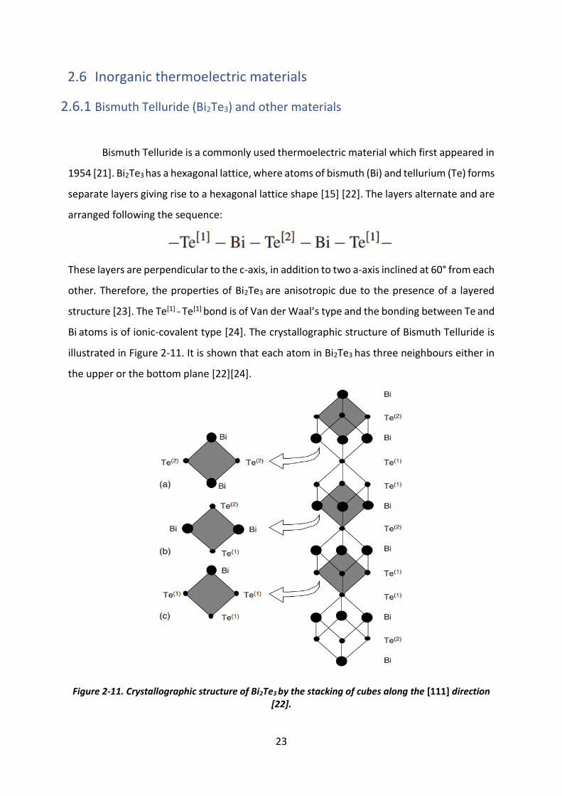
23
2.6 Inorganic thermoelectric materials
2.6.1 Bismuth Telluride (Bi2Te3) and other materials
Bismuth Telluride is a commonly used thermoelectric material which first appeared in
1954 [21]. Bi2Te3 has a hexagonal lattice, where atoms of bismuth (Bi) and tellurium (Te) forms
separate layers giving rise to a hexagonal lattice shape [15] [22]. The layers alternate and are
arranged following the sequence:
These layers are perpendicular to the c-axis, in addition to two a-axis inclined at 60° from each
other. Therefore, the properties of Bi2Te3 are anisotropic due to the presence of a layered
structure [23]. The Te[1] _ Te[1] bond is of Van der Waal’s type and the bonding between Te and
Bi atoms is of ionic-covalent type [24]. The crystallographic structure of Bismuth Telluride is
illustrated in Figure 2-11. It is shown that each atom in Bi2Te3 has three neighbours either in
the upper or the bottom plane [22][24].
Figure 2-11. Crystallographic structure of Bi2Te3 by the stacking of cubes along the [111] direction [22].
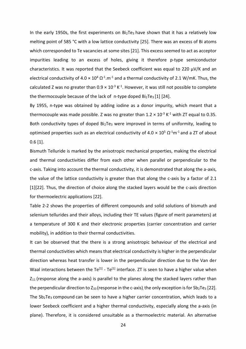
24
In the early 1950s, the first experiments on Bi2Te3 have shown that it has a relatively low
melting point of 585 °C with a low lattice conductivity [25]. There was an excess of Bi atoms
which corresponded to Te vacancies at some sites [21]. This excess seemed to act as acceptor
impurities leading to an excess of holes, giving it therefore p-type semiconductor
characteristics. It was reported that the Seebeck coefficient was equal to 220 µV/K and an
electrical conductivity of 4.0 × 10⁴ Ω-1.m-1 and a thermal conductivity of 2.1 W/mK. Thus, the
calculated Z was no greater than 0.9 × 10⁻³ K-1. However, it was still not possible to complete
the thermocouple because of the lack of n-type doped Bi2Te3 [1] [24].
By 1955, n-type was obtained by adding iodine as a donor impurity, which meant that a
thermocouple was made possible. Z was no greater than 1.2 × 10⁻³ K-1 with ZT equal to 0.35.
Both conductivity types of doped Bi2Te3 were improved in terms of uniformity, leading to
optimised properties such as an electrical conductivity of 4.0 × 10⁵ Ω-1m-1 and a ZT of about
0.6 [1].
Bismuth Telluride is marked by the anisotropic mechanical properties, making the electrical
and thermal conductivities differ from each other when parallel or perpendicular to the
c-axis. Taking into account the thermal conductivity, it is demonstrated that along the a-axis,
the value of the lattice conductivity is greater than that along the c-axis by a factor of 2.1
[1][22]. Thus, the direction of choice along the stacked layers would be the c-axis direction
for thermoelectric applications [22].
Table 2-2 shows the properties of different compounds and solid solutions of bismuth and
selenium tellurides and their alloys, including their TE values (figure of merit parameters) at
a temperature of 300 K and their electronic properties (carrier concentration and carrier
mobility), in addition to their thermal conductivities.
It can be observed that the there is a strong anisotropic behaviour of the electrical and
thermal conductivities which means that electrical conductivity is higher in the perpendicular
direction whereas heat transfer is lower in the perpendicular direction due to the Van der
Waal interactions between the Te[1] - Te[1] interface. ZT is seen to have a higher value when
Z11 (response along the a-axis) is parallel to the planes along the stacked layers rather than
the perpendicular direction to Z33 (response in the c-axis), the only exception is for Sb2Te3 [22].
The Sb2Te3 compound can be seen to have a higher carrier concentration, which leads to a
lower Seebeck coefficient and a higher thermal conductivity, especially along the a-axis (in
plane). Therefore, it is considered unsuitable as a thermoelectric material. An alternative
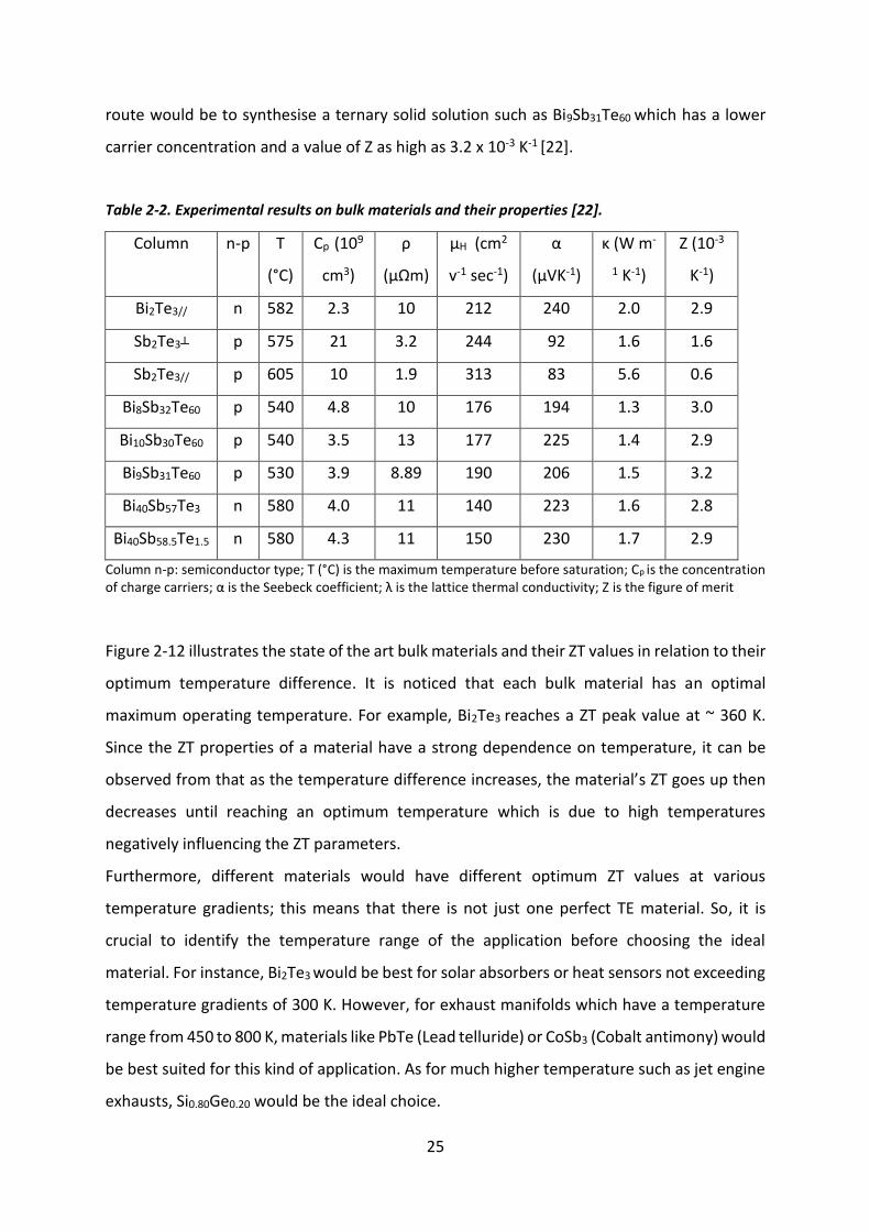
25
route would be to synthesise a ternary solid solution such as Bi9Sb31Te60 which has a lower
carrier concentration and a value of Z as high as 3.2 x 10⁻³ K-1 [22].
Table 2-2. Experimental results on bulk materials and their properties [22].
Column n-p T
(°C)
Cp (109
cm3)
ρ
(µΩm)
µH (cm2
v-1 sec-1)
α
(µVK-1)
κ (W m-
1 K-1)
Z (10-3
K-1)
Bi2Te3// n 582 2.3 10 212 240 2.0 2.9
Sb2Te3┴ p 575 21 3.2 244 92 1.6 1.6
Sb2Te3// p 605 10 1.9 313 83 5.6 0.6
Bi8Sb32Te60 p 540 4.8 10 176 194 1.3 3.0
Bi10Sb30Te60 p 540 3.5 13 177 225 1.4 2.9
Bi9Sb31Te60 p 530 3.9 8.89 190 206 1.5 3.2
Bi40Sb57Te3 n 580 4.0 11 140 223 1.6 2.8
Bi40Sb58.5Te1.5 n 580 4.3 11 150 230 1.7 2.9
Column n-p: semiconductor type; T (°C) is the maximum temperature before saturation; Cp is the concentration of charge carriers; α is the Seebeck coefficient; λ is the lattice thermal conductivity; Z is the figure of merit
Figure 2-12 illustrates the state of the art bulk materials and their ZT values in relation to their
optimum temperature difference. It is noticed that each bulk material has an optimal
maximum operating temperature. For example, Bi2Te3 reaches a ZT peak value at ~ 360 K.
Since the ZT properties of a material have a strong dependence on temperature, it can be
observed from that as the temperature difference increases, the material’s ZT goes up then
decreases until reaching an optimum temperature which is due to high temperatures
negatively influencing the ZT parameters.
Furthermore, different materials would have different optimum ZT values at various
temperature gradients; this means that there is not just one perfect TE material. So, it is
crucial to identify the temperature range of the application before choosing the ideal
material. For instance, Bi2Te3 would be best for solar absorbers or heat sensors not exceeding
temperature gradients of 300 K. However, for exhaust manifolds which have a temperature
range from 450 to 800 K, materials like PbTe (Lead telluride) or CoSb3 (Cobalt antimony) would
be best suited for this kind of application. As for much higher temperature such as jet engine
exhausts, Si0.80Ge0.20 would be the ideal choice.
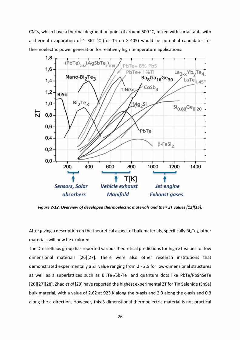
26
CNTs, which have a thermal degradation point of around 500 ˚C, mixed with surfactants with
a thermal evaporation of ~ 362 ˚C (for Triton X-405) would be potential candidates for
thermoelectric power generation for relatively high temperature applications.
Figure 2-12. Overview of developed thermoelectric materials and their ZT values [12][15].
After giving a description on the theoretical aspect of bulk materials, specifically Bi2Te3, other
materials will now be explored.
The Dresselhaus group has reported various theoretical predictions for high ZT values for low
dimensional materials [26][27]. There were also other research institutions that
demonstrated experimentally a ZT value ranging from 2 - 2.5 for low-dimensional structures
as well as a superlattices such as Bi2Te3/Sb2Te3 and quantum dots like PbTe/PbSnSeTe
[26][27][28]. Zhao et al [29] have reported the highest experimental ZT for Tin Selenide (SnSe)
bulk material, with a value of 2.62 at 923 K along the b-axis and 2.3 along the c-axis and 0.3
along the a-direction. However, this 3-dimenstional thermoelectric material is not practical
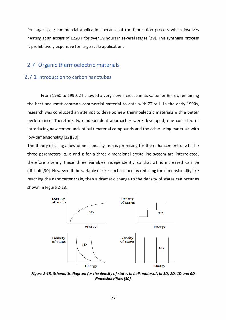
27
for large scale commercial application because of the fabrication process which involves
heating at an excess of 1220 K for over 19 hours in several stages [29]. This synthesis process
is prohibitively expensive for large scale applications.
2.7 Organic thermoelectric materials
2.7.1 Introduction to carbon nanotubes
From 1960 to 1990, ZT showed a very slow increase in its value for Bi2Te3, remaining
the best and most common commercial material to date with ZT ≈ 1. In the early 1990s,
research was conducted an attempt to develop new thermoelectric materials with a better
performance. Therefore, two independent approaches were developed; one consisted of
introducing new compounds of bulk material compounds and the other using materials with
low-dimensionality [12][30].
The theory of using a low-dimensional system is promising for the enhancement of ZT. The
three parameters, α, σ and κ for a three-dimensional crystalline system are interrelated,
therefore altering these three variables independently so that ZT is increased can be
difficult [30]. However, if the variable of size can be tuned by reducing the dimensionality like
reaching the nanometer scale, then a dramatic change to the density of states can occur as
shown in Figure 2-13.
Figure 2-13. Schematic diagram for the density of states in bulk materials in 3D, 2D, 1D and 0D dimensionalities [30].
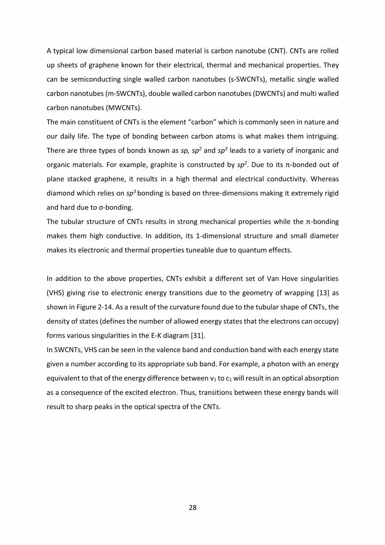
28
A typical low dimensional carbon based material is carbon nanotube (CNT). CNTs are rolled
up sheets of graphene known for their electrical, thermal and mechanical properties. They
can be semiconducting single walled carbon nanotubes (s-SWCNTs), metallic single walled
carbon nanotubes (m-SWCNTs), double walled carbon nanotubes (DWCNTs) and multi walled
carbon nanotubes (MWCNTs).
The main constituent of CNTs is the element “carbon” which is commonly seen in nature and
our daily life. The type of bonding between carbon atoms is what makes them intriguing.
There are three types of bonds known as sp, sp2 and sp3 leads to a variety of inorganic and
organic materials. For example, graphite is constructed by sp2. Due to its π-bonded out of
plane stacked graphene, it results in a high thermal and electrical conductivity. Whereas
diamond which relies on sp3 bonding is based on three-dimensions making it extremely rigid
and hard due to σ-bonding.
The tubular structure of CNTs results in strong mechanical properties while the π-bonding
makes them high conductive. In addition, its 1-dimensional structure and small diameter
makes its electronic and thermal properties tuneable due to quantum effects.
In addition to the above properties, CNTs exhibit a different set of Van Hove singularities
(VHS) giving rise to electronic energy transitions due to the geometry of wrapping [13] as
shown in Figure 2-14. As a result of the curvature found due to the tubular shape of CNTs, the
density of states (defines the number of allowed energy states that the electrons can occupy)
forms various singularities in the E-K diagram [31].
In SWCNTs, VHS can be seen in the valence band and conduction band with each energy state
given a number according to its appropriate sub band. For example, a photon with an energy
equivalent to that of the energy difference between v1 to c1 will result in an optical absorption
as a consequence of the excited electron. Thus, transitions between these energy bands will
result to sharp peaks in the optical spectra of the CNTs.
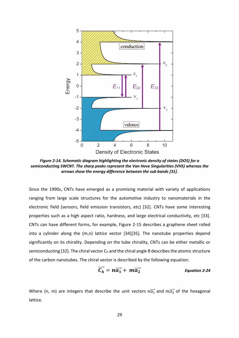
29
Figure 2-14. Schematic diagram highlighting the electronic density of states (DOS) for a semiconducting SWCNT. The sharp peaks represent the Van Hove Singularities (VHS) whereas the
arrows show the energy difference between the sub bands [31].
Since the 1990s, CNTs have emerged as a promising material with variety of applications
ranging from large scale structures for the automotive industry to nanomaterials in the
electronic field (sensors, field emission transistors, etc) [32]. CNTs have some interesting
properties such as a high aspect ratio, hardness, and large electrical conductivity, etc [33].
CNTs can have different forms, for example, Figure 2-15 describes a graphene sheet rolled
into a cylinder along the (m,n) lattice vector [34][35]. The nanotube properties depend
significantly on its chirality. Depending on the tube chirality, CNTs can be either metallic or
semiconducting [32]. The chiral vector Ch and the chiral angle θ describes the atomic structure
of the carbon nanotubes. The chiral vector is described by the following equation:
𝑪𝒉⃗⃗ ⃗⃗ = 𝒏𝒂𝟏⃗⃗ ⃗⃗ + 𝒎𝒂𝟐⃗⃗ ⃗⃗ Equation 2-24
Where (n, m) are integers that describe the unit vectors 𝑛𝑎1⃗⃗⃗⃗ and 𝑚𝑎2⃗⃗⃗⃗ of the hexagonal
lattice.
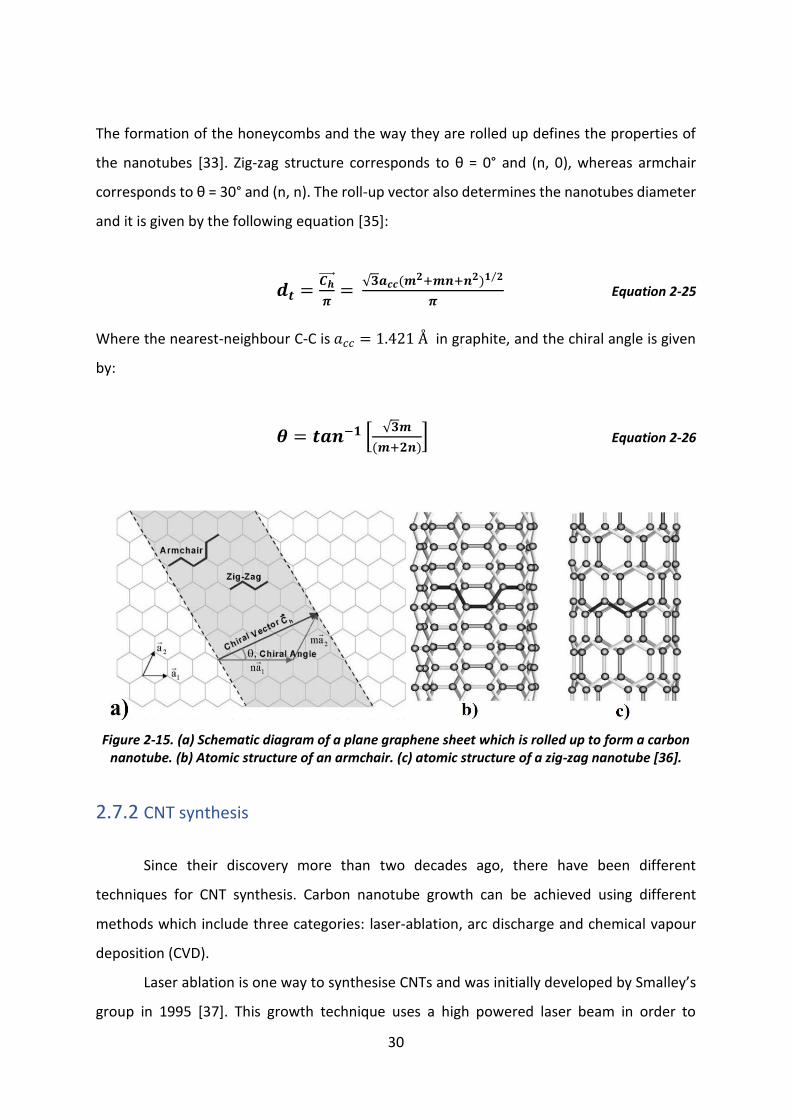
30
The formation of the honeycombs and the way they are rolled up defines the properties of
the nanotubes [33]. Zig-zag structure corresponds to θ = 0° and (n, 0), whereas armchair
corresponds to θ = 30° and (n, n). The roll-up vector also determines the nanotubes diameter
and it is given by the following equation [35]:
𝒅𝒕 =𝑪𝒉⃗⃗⃗⃗ ⃗
𝝅=
√𝟑𝒂𝒄𝒄(𝒎𝟐+𝒎𝒏+𝒏𝟐)𝟏 𝟐⁄
𝝅 Equation 2-25
Where the nearest-neighbour C-C is 𝑎𝑐𝑐 = 1.421 Å in graphite, and the chiral angle is given
by:
𝜽 = 𝒕𝒂𝒏−𝟏 [√𝟑𝒎
(𝒎+𝟐𝒏)] Equation 2-26
Figure 2-15. (a) Schematic diagram of a plane graphene sheet which is rolled up to form a carbon nanotube. (b) Atomic structure of an armchair. (c) atomic structure of a zig-zag nanotube [36].
2.7.2 CNT synthesis
Since their discovery more than two decades ago, there have been different
techniques for CNT synthesis. Carbon nanotube growth can be achieved using different
methods which include three categories: laser-ablation, arc discharge and chemical vapour
deposition (CVD).
Laser ablation is one way to synthesise CNTs and was initially developed by Smalley’s
group in 1995 [37]. This growth technique uses a high powered laser beam in order to
31
vaporise a graphite target which is mixed with a catalyst. This method is known for its high
yield that can reach as high as 70% resulting in less impurities than the arc-Discharge
method [38].
Figure 2-16 shows a typical configuration of a laser-ablation system. In a furnace of 1200 ˚C,
a target is scanned by a neodymium doped yttrium aluminium garnet (Nd:YAG). An inert gas
(argon) is used to blow the as-grown CNTs and deposit them on a soot collector. The target
used for CNT growth can have various compositions such as: iron (Fe), cobalt (Co), nickel (Ni)
and yttrium (Y).
In summary, laser-ablation is a physical technique commonly used in the industry. However,
it has a common issue consisting in the presence of impurities which requires a
post-treatment, thus, increasing manufacturing cost.
Figure 2-16. Schematic diagram of the laser ablation method. A graphitic target mixed with a catalyst is hit by a high beam laser resulting in CNTs which are deposited on a collector [39].
On the other hand, the arc discharge method is well-used as an industrial technique
[40] first proposed by Iijima et al [41] and Bethune et al [42]. It is commonly used to produce
single-walled tubes of high quality in a short time where a high current is applied into a
pressurized chamber heated at high temperature. It relies on vaporising graphite which will
in turn condensate to form CNTs [43]. Consequently, a catalyst (Fe, Co, Ni, etc) is required for
single wall carbon nanotubes (SWCNT) growth but it is not needed for multi wall carbon
nanotubes (MWCNTs). A typical setup for the arc-Discharge is shown in Figure 2-17 where a
constant current flows through two electrodes (cathode and anode). This results in a resistive
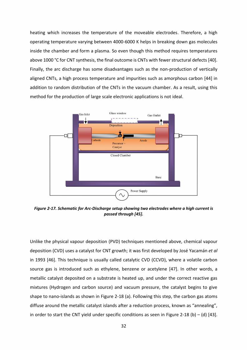
32
heating which increases the temperature of the moveable electrodes. Therefore, a high
operating temperature varying between 4000-6000 K helps in breaking down gas molecules
inside the chamber and form a plasma. So even though this method requires temperatures
above 1000 °C for CNT synthesis, the final outcome is CNTs with fewer structural defects [40].
Finally, the arc discharge has some disadvantages such as the non-production of vertically
aligned CNTs, a high process temperature and impurities such as amorphous carbon [44] in
addition to random distribution of the CNTs in the vacuum chamber. As a result, using this
method for the production of large scale electronic applications is not ideal.
Figure 2-17. Schematic for Arc-Discharge setup showing two electrodes where a high current is passed through [45].
Unlike the physical vapour deposition (PVD) techniques mentioned above, chemical vapour
deposition (CVD) uses a catalyst for CNT growth; it was first developed by José Yacamán et al
in 1993 [46]. This technique is usually called catalytic CVD (CCVD), where a volatile carbon
source gas is introduced such as ethylene, benzene or acetylene [47]. In other words, a
metallic catalyst deposited on a substrate is heated up, and under the correct reactive gas
mixtures (Hydrogen and carbon source) and vacuum pressure, the catalyst begins to give
shape to nano-islands as shown in Figure 2-18 (a). Following this step, the carbon gas atoms
diffuse around the metallic catalyst islands after a reduction process, known as “annealing”,
in order to start the CNT yield under specific conditions as seen in Figure 2-18 (b) – (d) [43].
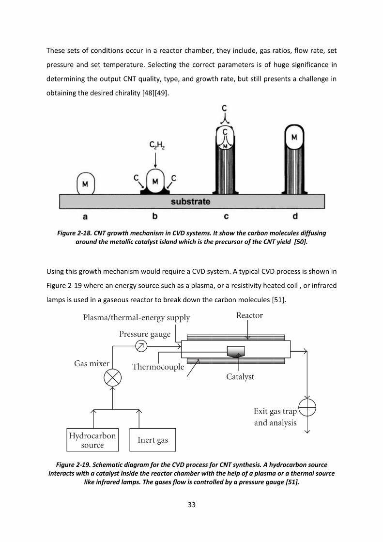
33
These sets of conditions occur in a reactor chamber, they include, gas ratios, flow rate, set
pressure and set temperature. Selecting the correct parameters is of huge significance in
determining the output CNT quality, type, and growth rate, but still presents a challenge in
obtaining the desired chirality [48][49].
Figure 2-18. CNT growth mechanism in CVD systems. It show the carbon molecules diffusing around the metallic catalyst island which is the precursor of the CNT yield [50].
Using this growth mechanism would require a CVD system. A typical CVD process is shown in
Figure 2-19 where an energy source such as a plasma, or a resistivity heated coil , or infrared
lamps is used in a gaseous reactor to break down the carbon molecules [51].
Figure 2-19. Schematic diagram for the CVD process for CNT synthesis. A hydrocarbon source interacts with a catalyst inside the reactor chamber with the help of a plasma or a thermal source
like infrared lamps. The gases flow is controlled by a pressure gauge [51].
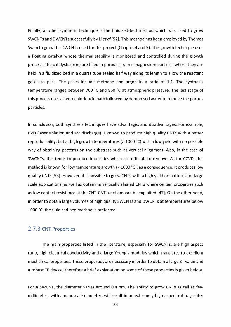
34
Finally, another synthesis technique is the fluidized-bed method which was used to grow
SWCNTs and DWCNTs successfully by Li et al [52]. This method has been employed by Thomas
Swan to grow the DWCNTs used for this project (Chapter 4 and 5). This growth technique uses
a floating catalyst whose thermal stability is monitored and controlled during the growth
process. The catalysts (iron) are filled in porous ceramic magnesium particles where they are
held in a fluidized bed in a quartz tube sealed half way along its length to allow the reactant
gases to pass. The gases include methane and argon in a ratio of 1:1. The synthesis
temperature ranges between 760 ˚C and 860 ˚C at atmospheric pressure. The last stage of
this process uses a hydrochloric acid bath followed by demonised water to remove the porous
particles.
In conclusion, both synthesis techniques have advantages and disadvantages. For example,
PVD (laser ablation and arc discharge) is known to produce high quality CNTs with a better
reproducibility, but at high growth temperatures (> 1000 °C) with a low yield with no possible
way of obtaining patterns on the substrate such as vertical alignment. Also, in the case of
SWCNTs, this tends to produce impurities which are difficult to remove. As for CCVD, this
method is known for low temperature growth (< 1000 °C), as a consequence, it produces low
quality CNTs [53]. However, it is possible to grow CNTs with a high yield on patterns for large
scale applications, as well as obtaining vertically aligned CNTs where certain properties such
as low contact resistance at the CNT-CNT junctions can be exploited [47]. On the other hand,
in order to obtain large volumes of high quality SWCNTs and DWCNTs at temperatures below
1000 ˚C, the fluidized bed method is preferred.
2.7.3 CNT Properties
The main properties listed in the literature, especially for SWCNTs, are high aspect
ratio, high electrical conductivity and a large Young’s modulus which translates to excellent
mechanical properties. These properties are necessary in order to obtain a large ZT value and
a robust TE device, therefore a brief explanation on some of these properties is given below.
For a SWCNT, the diameter varies around 0.4 nm. The ability to grow CNTs as tall as few
millimetres with a nanoscale diameter, will result in an extremely high aspect ratio, greater
35
than 106, as previously reported [54]. As a result, when using the CVD growth techniques,
vertical alignment coupled with high aspect ratio of the CNTs allows a considerable increase
in the CNT surface area. This property is particularly important when considering
functionalization since it allows dopants such as surfactants that disperse CNTs to attach their
molecules onto a single CNT shell, therefore altering their electronic properties. Additionally,
if considering VACNTs for potential TE devices, the high aspect ratio gives the possibility to
include a large number of thermoelectric elements (n-type and p-type semiconductors) in
very small substrates, resulting in high output current. Carbon nanotubes are able to break
the link between electrical and thermal conductivity because they are very good thermal
emitters (blackbodies); although heat is transmitted via phonons through the length of the
tube, a larger proportion is lost through emission, as is also shown later in Chapter 3 (Section
3.2), where we show that, for a random CNT film, the optimum device length is ~1 cm. For a
vertically-aligned CNT device, this is likely to be higher as we do not have the losses associated
with CNT-to-CNT junctions. This length limit was observed almost independently of doping or
surfactant, within the resolution of our experiment, which indicates that doping is a
secondary thermal effect, whilst it will strongly influence electrical conductivity and can thus
improve the ZT of the device. Lastly, the current produced by a TE device made of
semiconducting SWCNTs will increase with the number of vertically aligned SWCNTs resulting
in a high output power but, as discussed in Section 2.2 (TE design considerations), this will
increase the current generated only. So, to also increase the output voltage, parallel n and p
pairs of elements are needed.
Due to the CNT nanoscale dimensions, especially SWCNTs, they have emerged as promising
materials for electronic applications. Understanding the importance of their electrical
properties and because they are considered one dimensional wires, has led to investigating
ballistic conduction in CNTs, the extremely high charge carrier mobility (~106 cm2/V.s) and the
large current carrying capacity (>109 A/cm2) [55][56][57]. Conversely, the presence of
structural defects in CNTs will hinder the transport properties of the charge carriers due to a
large number of sites (holes within a CNT), however, this can be generally overcome if the
appropriate functionalization dopant is introduced where these molecules can bond to the
carbon molecules filling the empty sites.
Another property is the high mechanical strength because of a large Young’s modulus
measured to be as high as 1 TPa, which is five times greater than steel [58]. In addition, CNTs
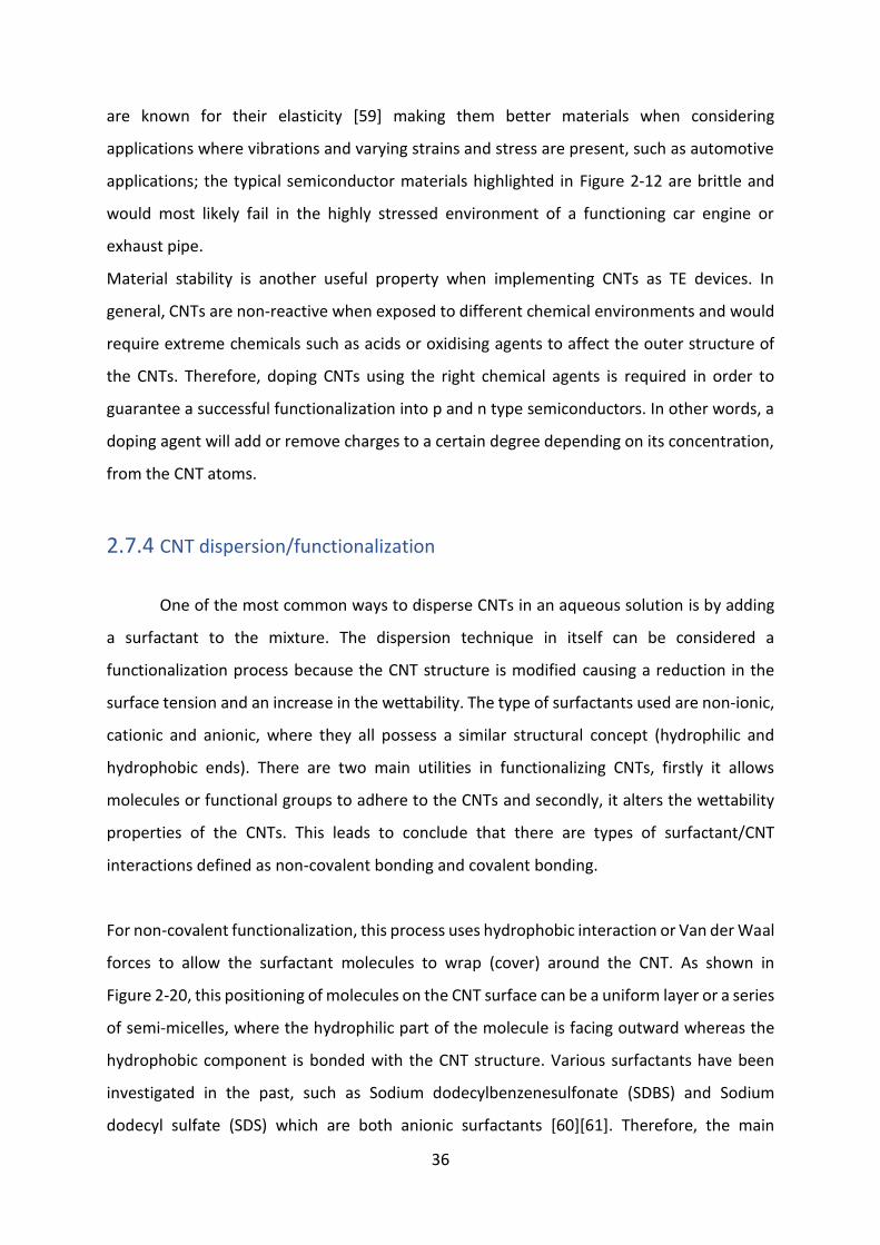
36
are known for their elasticity [59] making them better materials when considering
applications where vibrations and varying strains and stress are present, such as automotive
applications; the typical semiconductor materials highlighted in Figure 2-12 are brittle and
would most likely fail in the highly stressed environment of a functioning car engine or
exhaust pipe.
Material stability is another useful property when implementing CNTs as TE devices. In
general, CNTs are non-reactive when exposed to different chemical environments and would
require extreme chemicals such as acids or oxidising agents to affect the outer structure of
the CNTs. Therefore, doping CNTs using the right chemical agents is required in order to
guarantee a successful functionalization into p and n type semiconductors. In other words, a
doping agent will add or remove charges to a certain degree depending on its concentration,
from the CNT atoms.
2.7.4 CNT dispersion/functionalization
One of the most common ways to disperse CNTs in an aqueous solution is by adding
a surfactant to the mixture. The dispersion technique in itself can be considered a
functionalization process because the CNT structure is modified causing a reduction in the
surface tension and an increase in the wettability. The type of surfactants used are non-ionic,
cationic and anionic, where they all possess a similar structural concept (hydrophilic and
hydrophobic ends). There are two main utilities in functionalizing CNTs, firstly it allows
molecules or functional groups to adhere to the CNTs and secondly, it alters the wettability
properties of the CNTs. This leads to conclude that there are types of surfactant/CNT
interactions defined as non-covalent bonding and covalent bonding.
For non-covalent functionalization, this process uses hydrophobic interaction or Van der Waal
forces to allow the surfactant molecules to wrap (cover) around the CNT. As shown in
Figure 2-20, this positioning of molecules on the CNT surface can be a uniform layer or a series
of semi-micelles, where the hydrophilic part of the molecule is facing outward whereas the
hydrophobic component is bonded with the CNT structure. Various surfactants have been
investigated in the past, such as Sodium dodecylbenzenesulfonate (SDBS) and Sodium
dodecyl sulfate (SDS) which are both anionic surfactants [60][61]. Therefore, the main
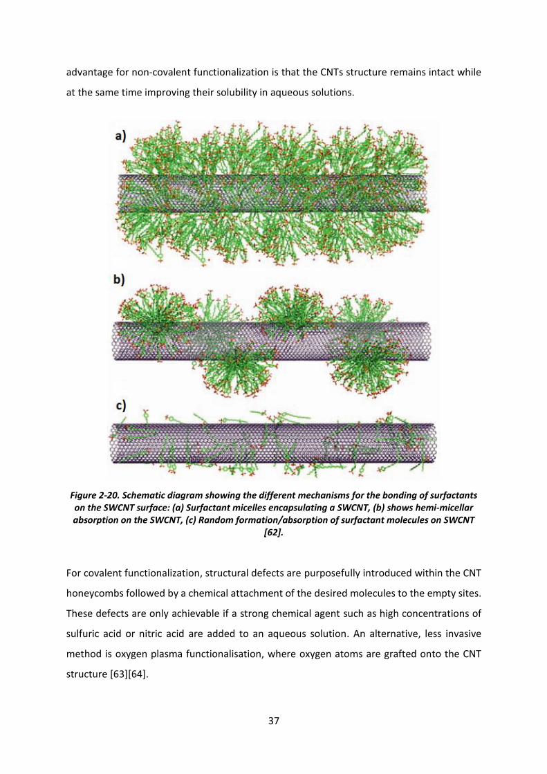
37
advantage for non-covalent functionalization is that the CNTs structure remains intact while
at the same time improving their solubility in aqueous solutions.
Figure 2-20. Schematic diagram showing the different mechanisms for the bonding of surfactants on the SWCNT surface: (a) Surfactant micelles encapsulating a SWCNT, (b) shows hemi-micellar absorption on the SWCNT, (c) Random formation/absorption of surfactant molecules on SWCNT
[62].
For covalent functionalization, structural defects are purposefully introduced within the CNT
honeycombs followed by a chemical attachment of the desired molecules to the empty sites.
These defects are only achievable if a strong chemical agent such as high concentrations of
sulfuric acid or nitric acid are added to an aqueous solution. An alternative, less invasive
method is oxygen plasma functionalisation, where oxygen atoms are grafted onto the CNT
structure [63][64].
38
In addition to ionic surfactants, non-ionic surfactants have also been reported to effectively
disperse CNTs such as Polyethylene glycol hexadecyl ether (Brij 58), Polyethylene glycol
sorbitan monooleate (Tween 80), Poloxamer (Pluronic F-127) and Polyethylene glycol tert-
octylphenyl ether (Triton X-405) which will be used for this project to determine the electrical
properties of each one and how they can affect each parameter.
2.7.5 Surfactant selection
Surfactants are differentiated by both the properties of their hydrophilic and
hydrophobic groups. In an aqueous solution, the hydrophilic end (tail) of a surfactant which
is facing outward can be anionic (negative charge), cationic (positive charge), zwitterionic
(positive and negative charge) or non-ionic (no apparent charge). As for the hydrophobic end
which adheres to the CNT structure, the majority of the surfactants are made up of a linear
chain of hydrocarbons [65]. The hydrocarbon chains can have different structural lengths
ranging between C8 to C20. Since most surfactants are used as detergents, their combined
roles include: absorption, change in the surface tension and interfacial tension, formation of
Micelles in water, wetting of solids, dispersing/aggregation of solids, foaming/defoaming and
emulsifying/demulsifying, etc [65]. Therefore, a brief explanation on some of these roles and
what is happening between CNTs and surfactant molecules is necessary.
Firstly, Absorption is the initial step of the interaction process between a surfactant and a
material. At first glance, a surfactant’s major characteristic is to be at higher concentration at
the surface than in the bulk liquid. This behaviour can occur at various interfaces such as
liquid/liquid interface, solid/liquid interface, etc. Taking the example of our experimental
work, which is an air/water surface, it was noticed that the more surfactant there is to
completely cover the top of the water surface, the more the physical and chemical changes
that occur at that interface. This can be further explained by understanding the effect of the
surface tension where it decreases as a function of an increase in the surfactant concentration
up to the point where a monolayer of a surfactant is formed, causing the surface tension to
level off as seen in Figure 2-21 below.
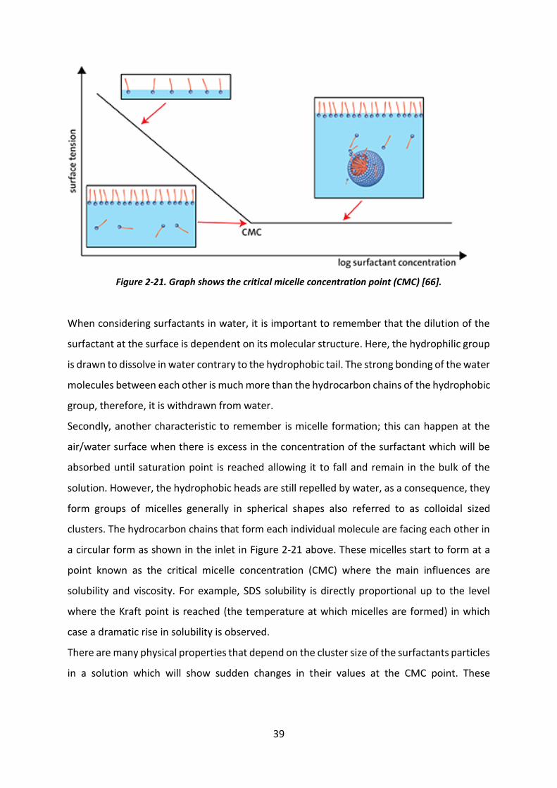
39
Figure 2-21. Graph shows the critical micelle concentration point (CMC) [66].
When considering surfactants in water, it is important to remember that the dilution of the
surfactant at the surface is dependent on its molecular structure. Here, the hydrophilic group
is drawn to dissolve in water contrary to the hydrophobic tail. The strong bonding of the water
molecules between each other is much more than the hydrocarbon chains of the hydrophobic
group, therefore, it is withdrawn from water.
Secondly, another characteristic to remember is micelle formation; this can happen at the
air/water surface when there is excess in the concentration of the surfactant which will be
absorbed until saturation point is reached allowing it to fall and remain in the bulk of the
solution. However, the hydrophobic heads are still repelled by water, as a consequence, they
form groups of micelles generally in spherical shapes also referred to as colloidal sized
clusters. The hydrocarbon chains that form each individual molecule are facing each other in
a circular form as shown in the inlet in Figure 2-21 above. These micelles start to form at a
point known as the critical micelle concentration (CMC) where the main influences are
solubility and viscosity. For example, SDS solubility is directly proportional up to the level
where the Kraft point is reached (the temperature at which micelles are formed) in which
case a dramatic rise in solubility is observed.
There are many physical properties that depend on the cluster size of the surfactants particles
in a solution which will show sudden changes in their values at the CMC point. These
40
properties include: detergency, equivalent conductivity, surface tension, interfacial tension,
light scattering and refractive index, etc.
It is thought that the hydrophobic groups of surfactants dissolved in solutions cause
distortions to the water structure thereby its free energy increases [67]. This is eliminated by
the increase in concentration of surfactant molecules at the surface and the orientation of
the hydrophobic ends away from the solvent. On the other hand, one way of reducing the
system’s free energy is micellization. However, for polar surfactants (anionic and cationic) and
non-polar surfactants (non-ionic that do not have Ethylene Oxide groups), increasing the
temperature of the solution tends to decrease the number of aggregated clusters due to the
high kinetic energy of the molecules.
Solubility is yet another parameter which is important to the field of surfactants. The best
way to increase the solubility of surfactants is to increase the temperature of the aqueous
solution.
Lastly, dispersion is also a characteristic used in this project where individual CNTs are
separated from each other. When a solid (e.g. CNT) particle is added to a liquid solution like
water, its suspension is facilitated by the use of a surfactant which will allow the particles to
be stable and spread uniformly within the bulk of the solution. Solids added to a large volume
of water will create new interfaces of solid/liquid, as a consequence, the surfactant’s role in
this case is to reduce the interfacial energy therefore resulting in the formation of new
interfaces [68].
Choosing the ideal surfactant would depend on the type of charge on the hydrophilic group
and the type of surface (material) that will interact with it. For example, to make a material’s
surface (negatively charged) hydrophobic then a cationic surfactant is ideal. The surface will
absorb the surfactant with its positive polar group contained in the hydrophilic head, which
is facing towards the surface with negative charge due to electrostatic forces (attraction),
whereas the hydrophobic group is oriented away from the surface making it water repellent.
However, if the surface is to be characterised as water-wettable (hydrophilic), then cationic
surfactants should be avoided [67].
On the other hand, non-ionics which have no apparent ionic charge (neutral) tend to be an
all-purpose surfactant since they can absorb onto surfaces with either the hydrophilic or
hydrophobic group orientated towards the surface, depending on its charge.
41
2.8 Optimisation of Thermoelectric properties
2.8.1 Increasing the power factor
The power factor is defined as the product of the Seebeck coefficient squared and the
electrical conductivity (α2 σ). These two parameters are important since they depend strongly
on the charge carriers’ concentration. Therefore, obtaining a high figure of merit requires a
high carrier concentration which leads to a high power factor.
Increasing the power factor is an active research area that requires a deep investigation of
both Seebeck coefficient and electrical conductivity. As shown in Figure 2-7, an increase in
the electrical conductivity results to a reduction to the Seebeck coefficient.
An example of increasing the power factor in bulk materials is reported by Li et al [69]. It is
believed that incorporating hard Silicon carbide (SiC) nanoparticles into Bi2Te3-based alloys
can enhance not only the thermoelectric materials properties but also the device fabrication
[70]. It is demonstrated that in Bi0.3Sb1.7Te3 alloys, a ZT value as high as 1.33 at 373 K was
obtained just by introducing an optimised amount of nano-SiC particles. The highest electrical
conductivity was reported to be 10.2 x 10⁴ S/m when adding 0.4 vol% of SiC particles. However,
even though the carrier concentration increased from 1.81 x 1019 cm-3 to 3.39 x 1019 cm-3, the
carrier mobility subsequently decreased from 365.4 cm2 V-1 s-1 to 212.1 cm2 V-1 s-1. The
addition of SiC particles is understood to cause a reduction in grain size which lead to defect
increases, thus, the carrier density increases and the mobility decreases by improving
scattering [69]. It has also been revealed that the power factor showed a maximum value of
3.93 mW K-2 around 327 when adding SiC particles.
There were also reports of increasing the power factor in SWCNTs. Nonoguchi et al [71]
reported 33 organic compounds used as dopants for tuning p-type and n-type SWCNTs for
the usage of thermoelectric power conversion materials in a temperature under 400 K.
Among all the 33 compounds, 18 of them: (phosphine derivatives and amine-, and imine-
containing molecules) have been reported to have successfully switched p-type SWCNT into
n-type SWCNTs. A Seebeck coefficient of -72 µV/K was determined when SWCNT film was
doped with triphenylphosphine (tpp) compared to polyethyleneimine (PEI) doped SWCNTs
which had a value of -34 µV/K. The films doped with tpp and dppp
42
(1,3-bis(diphenylphosphino)propane) show the highest power factor, almost 2.5 times higher
than PEI doped SWCNTs with a value of 25 µW/mK2. This clearly shows that enhancing the
Seebeck coefficient improved the power factors significantly [71][72][73].
2.8.2 Minimising thermal conductivity
A typical way of reducing the thermal conductivity is by scattering of phonons on
different types of defects. Defects can scatter the charge carriers and the lattice vibrations.
However, electrons and holes have a greater mean free path than phonons therefore carrier
mobility is expected to be affected more than on the lattice conductivity. During experiments,
it seems that the mobility of the charge carriers to the lattice conductivity can be increased
via defect scattering [1][74]. In semiconductors, the study of heat and transport is critical if
the issue of a high ZT needs to be tackled. Thus, the knowledge on materials properties is
required and how thermal conductivity can be decreased in a selective way is critical.
It is important to take into account that thermal conductivity of a semiconductor includes two
components that transport heat: the electronic component κe (electrons and holes), the
lattice component κl (phonons travelling through lattice) [9]. The Widemann-Franz law
directly relates the electronic component to the electrical conductivity and it is given by [9]:
𝜿 = 𝜿𝒆 + 𝜿𝒍 Equation 2-27
and
𝜿𝒆 = 𝑳𝝈𝑻 = 𝒏𝒆𝝁𝑳𝑻 Equation 2-28
Where L is the Lorentzian factor (2.4 x 10⁻⁸ J2K-2 C-2), σ is the electrical conductivity, T is the
temperature, n is the carrier concentration, e is the electron charge and µ is the carrier
mobility.
Since the power factor is interrelated with the thermal conductivity, then reducing the latter
can decrease the power factor. Semiconducting TE materials are heavily doped when mixed
with compounds for the purpose of increasing the electrical conductivity. This will cause
electrons and holes in heat transport contribution. The significant presence of the electronic
43
components in a material needs to be taken into consideration when minimizing thermal
conductivity [9].
There are many ways to reduce the thermal conductivity of TE materials. For example, by
alloy disorder which is a mechanism that scatters phonons to improve the electrical thermal
conductivity ratio and has proven to be more effective than electron and holes scattering.
Scattering by other phonons, grain boundaries, introducing lattice defects tend to minimize
the phonon mean free path [74].
Furthermore, the manipulation of the thermoelectric properties of nanowires through
quantum confinement of electrons has shown promising developments in energy conversion
materials [75]. It is believed that phonon transport in nanowires can behave differently to
bulk semiconductors mainly due to the modification in the confinement where boundary
scattering can be much stronger than bulk semiconductors [76].
However, reports on thermal conductivity of bulk materials have shown that its contribution
results in a high ZT. This is due to the anisotropic and anharmonic bonding found within the
structure that led to a lattice thermal conductivity of 0.23 ± 0.03 W m-1 K-1 at 973 K in SnSe
[29].
Low dimensional structure materials on the other hand show a rather high thermal
conductivity but can be substantially reduced by quenching of phonon mode in bundles and
excessive heat radiation from the surface of nanotubes as demonstrated by Aliev et al [77].
The thermal conductivity found in MWCNTs grown by CVD method was 600 ± 100 W m-1 K-1
which is less than the predicted theoretical value for SWCNTs estimated to be
6600 W m-1 K-1 [77][78]. The latter value is due to the decreased phonon scattering in a one-
dimensional system as well as the direction of the measurement which is in the longitudinal
direction (along the CNT) [13]. It is demonstrated that coupling within the large bundles of
MWCNTs and within the inner walls of the MWCNTs would decrease its thermal conductivity
to 150 W m-1 K-1. This can suppress the phonon modes, therefore, reducing the heat transport
of individual MWCNTs. Sheets of MWCNTs further reduced thermal conductivity to 50 W m-1
K-1 due to the interconnections between the tubes and the sheet imperfections like
misalignment [77].
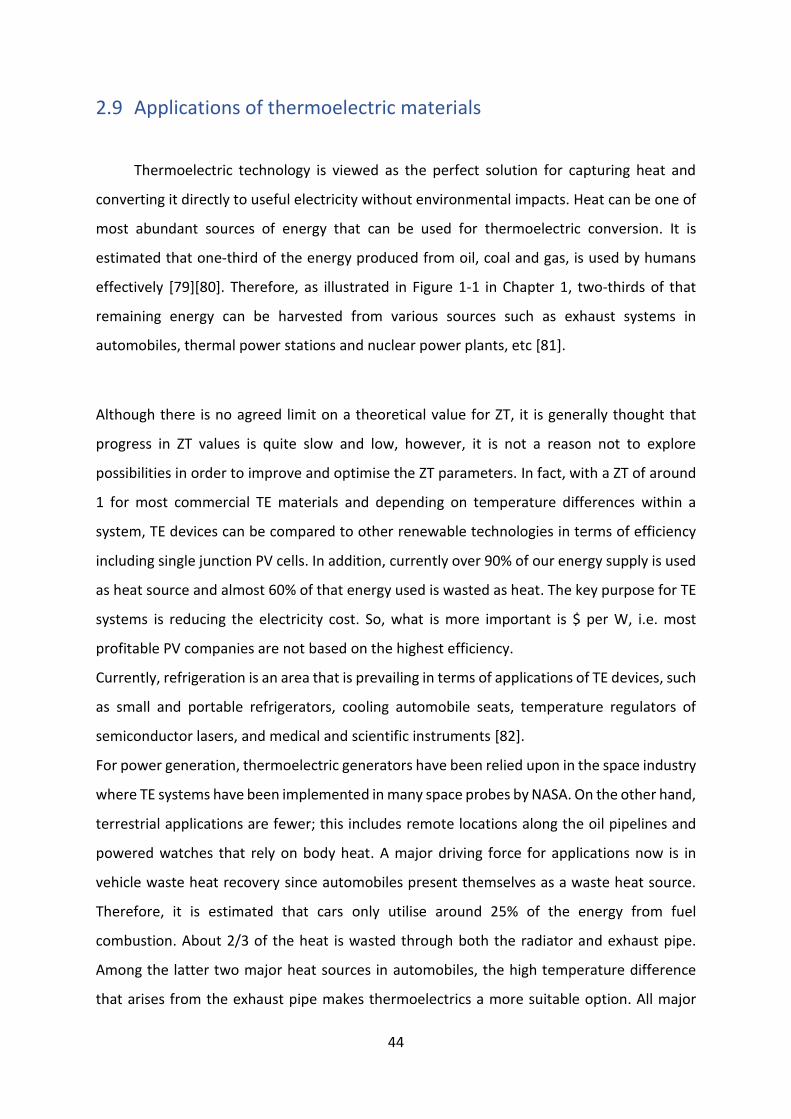
44
2.9 Applications of thermoelectric materials
Thermoelectric technology is viewed as the perfect solution for capturing heat and
converting it directly to useful electricity without environmental impacts. Heat can be one of
most abundant sources of energy that can be used for thermoelectric conversion. It is
estimated that one-third of the energy produced from oil, coal and gas, is used by humans
effectively [79][80]. Therefore, as illustrated in Figure 1-1 in Chapter 1, two-thirds of that
remaining energy can be harvested from various sources such as exhaust systems in
automobiles, thermal power stations and nuclear power plants, etc [81].
Although there is no agreed limit on a theoretical value for ZT, it is generally thought that
progress in ZT values is quite slow and low, however, it is not a reason not to explore
possibilities in order to improve and optimise the ZT parameters. In fact, with a ZT of around
1 for most commercial TE materials and depending on temperature differences within a
system, TE devices can be compared to other renewable technologies in terms of efficiency
including single junction PV cells. In addition, currently over 90% of our energy supply is used
as heat source and almost 60% of that energy used is wasted as heat. The key purpose for TE
systems is reducing the electricity cost. So, what is more important is $ per W, i.e. most
profitable PV companies are not based on the highest efficiency.
Currently, refrigeration is an area that is prevailing in terms of applications of TE devices, such
as small and portable refrigerators, cooling automobile seats, temperature regulators of
semiconductor lasers, and medical and scientific instruments [82].
For power generation, thermoelectric generators have been relied upon in the space industry
where TE systems have been implemented in many space probes by NASA. On the other hand,
terrestrial applications are fewer; this includes remote locations along the oil pipelines and
powered watches that rely on body heat. A major driving force for applications now is in
vehicle waste heat recovery since automobiles present themselves as a waste heat source.
Therefore, it is estimated that cars only utilise around 25% of the energy from fuel
combustion. About 2/3 of the heat is wasted through both the radiator and exhaust pipe.
Among the latter two major heat sources in automobiles, the high temperature difference
that arises from the exhaust pipe makes thermoelectrics a more suitable option. All major
45
automobile manufacturers have invested in thermoelectric program in order to investigate
and develop waste heat recovery technology. These programs are motivated by the strict
policies on CO2 emission imposed by governments. For example, in April 2009, the European
Parliament has set new standards (in emission performance) for new vehicles, reducing CO2
emissions from automobiles [83]. From 2012, it is estimated that a car manufacturer must
pay extra tax duty as a premium if their registered vehicles exceed the allowed emission limits.
Another factor which should motivate automotive industries to investing in Research and
Development in the sector of thermoelectrics is the ever-increasing price of oil and the
growing concern in its future availability. World renowned automobile makers such as BMW,
Volvo and General Motors are accelerating their pace in the development of energy-efficient
TE devices for heat recovery. It is widely thought that electric vehicles are the most-efficient
and environmentally friendly type of vehicles [84]. However, considering that producing
electricity in order to charge up an electric car requires natural sources like solar, gas, wind
and sea current; it renders this type of vehicles fully dependant on large infrastructures in
obtaining the energy needed to charge up the batteries. Therefore, they cannot compete
directly with petrol and diesel vehicles [85]. On the other hand, petrol and diesel vehicles will
always be a source of pollution. Consequently, to overcome these previous issues, one can
combine both systems, better known as hybrids. In recent years, the most efficient way of
transportation has been identified as hybrid electric vehicles, although they are not of
absolutely zero emission due to the use of fossil fuels [86]. Nonetheless, both hybrid vehicles
and fossil fuel vehicles use internal combustion engines (ICE) which is a very good source of
waste heat, as shown in Figure 2-22. It is estimated that about 40 % is lost as a form of heat,
with temperatures exceeding 500 ˚C at the exhaust manifold. This makes the use of
thermoelectric devices a very attractive option. The focus of research activities has been on
improving the operating temperature range and conversion efficiency of TE devices [87][88].
Converting this waste heat can positively impact an engine. For example, TE power generators
could contribute greatly in reducing fuel consumption by converting waste heat into
electricity, therefore, engine performance, reliability and efficiency could be significantly
improved. In addition, TE generators could reduce torque and horsepower losses by
eliminating secondary loads from the engine drivetrain which would help to decreasing
46
engine weight by disposing of certain components [88]. As a result, the full power produced
by the motor is directed by the drive shaft, thus improving performance and fuel economy.
However, TE power generators integrated onto the exhaust manifold can only function if the
ICE is burning fuel and not when the engine is off.
Figure 2-22. Energy flow in internal combustion engines [4].
As well as using TE generators as integrated systems for ICEs, TE technology could also lead
to implementing a reversible, reliable automotive air conditioning system that does not use
liquid coolants as refrigerants which raise concerns due to greenhouse gas emissions. This
could be integrated in a simpler and easier package making it more efficient to operate
especially if the TE devices used are flexible such as CNT films. Consequently, TE coolers come
with a disadvantage because they will certainly require more electrical power than current
mechanical systems [88].
In conclusion, considerations need to be addressed when using these TE generators after
purchasing such technology because it requires assessing the savings that a consumer makes.
In other words, the economic benefit needs to outweigh the cost. So before engineering a
system, fuel consumption should be used as a reference in order to consider system
implementation.
47
2.9.1 Solar thermal energy generation
Solar thermoelectric generator (STEG) is another application for TE devices. The idea
is to use concentrated solar energy to generate heat therefore creating electricity [89]. The
efficiency of STEGs is defined by the product of the opto-thermal efficiency and the device
efficiency. It was demonstrated experimentally by Kraemer et al [90] that a flat-panel STEG
with a high thermal concentration achieved a peak efficiency of 4.6 % under strong light arrays
of AM1.5G (1 kW m2). The resulting efficiency was 7-8 times higher than the previously
reported best value for a flat-panel STEG. A large output voltage requires a large temperature
difference between the two ends of a TE module, so instead of using costly systems such as
an optical concentrator, a highly solar-absorbing surface such as a blackbody (CNT film) is
used. The latter converts solar radiations into heat and with the use of thermal concentrators,
heat energy is directed onto the TE elements by means of lateral heat conduction. One
advantage of such a highly absorbing material (STEG) is that there is no requirement for a
tracking system, which in turn can be a cost effective technology for solar energy conversion
into electricity. In addition, it can also be integrated as solar collector tubes for producing hot
water; this shows the potential of STEGs for generating electricity and hot water
simultaneously. Figure 2-23 below illustrates a schematic of the STEG device. Some of the
literature has emphasized on the requirement of a high heat flux to be able to make
thermoelectric devices more efficient and viable. While such a system is useful in some other
applications, it is not ideal for waste heat, where energy conversion naturally involves lower
heat inputs. Therefore, it is believed that a TE device system efficiency will reduce if there is
a large mismatch in heat flux which eventually leads to extra drops in temperature differences
for TE devices.
Every year, the levelized cost (constant cost per unit of electric power generation), instant
cost, output power and overall performance of renewable systems are assessed by the energy
commissions which are then compared with alternative technologies in energy conversion
[91][92]. Since TE materials are not widely commercialized, they are not considered in these
evaluations. This means that it is up to the TE experts to analyse the cost and how it stacks up
with TE device performance. It is estimated that the capital cost of the TE elements varies
between 2$ - 5$ per Watt, and their life time is between 15 to 20 years, this makes
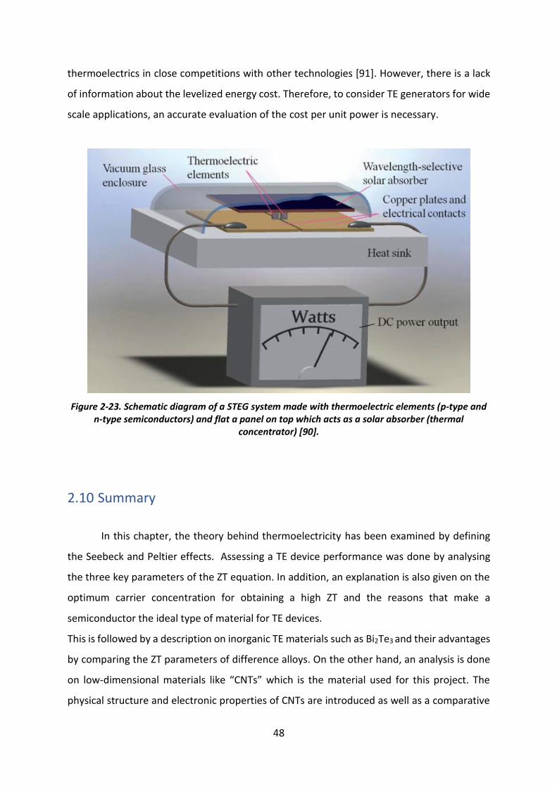
48
thermoelectrics in close competitions with other technologies [91]. However, there is a lack
of information about the levelized energy cost. Therefore, to consider TE generators for wide
scale applications, an accurate evaluation of the cost per unit power is necessary.
Figure 2-23. Schematic diagram of a STEG system made with thermoelectric elements (p-type and n-type semiconductors) and flat a panel on top which acts as a solar absorber (thermal
concentrator) [90].
2.10 Summary
In this chapter, the theory behind thermoelectricity has been examined by defining
the Seebeck and Peltier effects. Assessing a TE device performance was done by analysing
the three key parameters of the ZT equation. In addition, an explanation is also given on the
optimum carrier concentration for obtaining a high ZT and the reasons that make a
semiconductor the ideal type of material for TE devices.
This is followed by a description on inorganic TE materials such as Bi2Te3 and their advantages
by comparing the ZT parameters of difference alloys. On the other hand, an analysis is done
on low-dimensional materials like “CNTs” which is the material used for this project. The
physical structure and electronic properties of CNTs are introduced as well as a comparative
49
analysis on the different synthesis techniques used for growing CNTs. For this project, the
PTCVD which is described in Chapter 4 (Section 4.1), is the preferred technique due to its
ability to produce vertically aligned CNTs at low temperature growth.
Furthermore, the theory on the functionalization and dispersion of the CNTs is explored by
assessing the bonding of the hydrophobic tail to the CNT structure and the hydrophilic head
groups which face towards water. In addition, a description on the selection of the
requirements in selecting surfactants is also provided.
Finally, the importance of TE devices is stated by highlighting different applications of TE
devices such as hybrid systems and solar absorbers.
50
Characterisation techniques
As discussed in chapter 1, the main objective set for this project is to obtain a high
performance lightweight TE device composed of CNTs. This requires characterisation
techniques capable of accurately measuring different parameters over many length scales. In
this research, various analytical methods were used to probe samples in order to collect and
compare data with previous published work in the field of thermoelectrics. This has led to
novel directions that were key to achieving the targets set for this research. The theory and
experimental set up of the characterisation techniques used will be explained within this
Section, as well as the reasons behind why each method was selected for the project success.
3.1 Electrical conductivity measurement
Electrical conductivity is defined as a material’s ability to conduct electric current. It is
one of the key components of the ZT parameters. Measuring this accurately can help to
understand the behaviour and characteristics of the charge carriers. In addition, Chapter 5
will explain how the electrical conductivity is directly related to the Seebeck coefficient.
One of the challenges facing accurate measurements of electrical conductivity is the
geometry of the samples (CNT network, CNT rope, etc), which can significantly affect the
measured as well as the recorded values. In essence, it has been reported that conductivity
values for SWCNT films range from 12.5 S/cm [93] to ~ 10,000 S/cm [94]. Films made of HiPCo
SWCNTs dispersed using oleum were reported to have values from 900 - 1300 S/cm [95].
Other groups reported conductivity values for SWCNT films from 200 - 500 S/cm [38][96] [97].
However, for the axial conductivity of a SWCNT rope, as opposed to a film, all reported values
of CNT films were well below the range of 10,000 - 30,000 S/cm [98]. Therefore, it is believed
that the lower electrical conductivity values reported for SWCNT films are potentially due to
the misalignment or bundling of the CNTs, the increased number of Schottky barriers and
discontinuous contacts that arise in the form of tube-to-tube junctions, resulting in higher
resistances [99]. This inhomogeneity and lack of a consistent organised distribution of the
CNTs, cause various complications when measuring the electrical conductivity of a SWCNT
film. So, it is important to come up with an appropriate measurement method for CNT films.
51
In this instance, two methods were used for the conductivity measurements in order to
confirm the accuracy of the data; the Van der Pauw technique and the transmission line
measurement (TLM) technique. Both methods require the same key sets of conditions to be
met in order to be effectively used, such as: uniform shape, homogenous thickness and no
porosity. According to Zhou et al [100], it was claimed that a vacuum filtration technique
results in homogenous CNT films which meet the required key sets of conditions for the two
chosen electrical measurement methods. Therefore, as an identical filtration method was
used, it can be suggested that the CNT films in this project should also be suitable for these
measurement methods.
Both techniques require the calculation of the sheet resistance (Rs) in order to determine the
resistivity. The sheet resistance is defined as the resistance between two opposing edges of
the square sheet to be measured. The measuring current flows through a cross-Sectional area
(Wt), where (W) is the width and (t) is the thickness of the film. The length of the sample is
(L), therefore, the resistance R is given by the following expression [101]:
𝑹 = 𝝆 𝑳
𝑨 = 𝝆
𝑳
𝑾𝒕 Equation 3-1
Substituting for A gives: 𝑹𝒔 =𝝆
𝒕 Equation 3-2
Therefore, the sheet resistance is independent of the length L:
𝑹 = 𝑹𝒔𝑳
𝑾 Equation 3-3
So, the electrical resistivity 𝜌 and electrical conductivity 𝜎 can be defined as:
𝝆 = 𝑹𝒔𝒕 Equation 3-4
𝝈 = 𝟏
𝝆 Equation 3-5
For electrical characterisation, an analysis of examples of sets of data obtained from
the CNT films that will be described including their fabrication process in detail in Chapter 5.
The data analysis includes the standard deviation and the standard error. The former is
defined as a measure used to quantify the number of variations from multiple repeated data
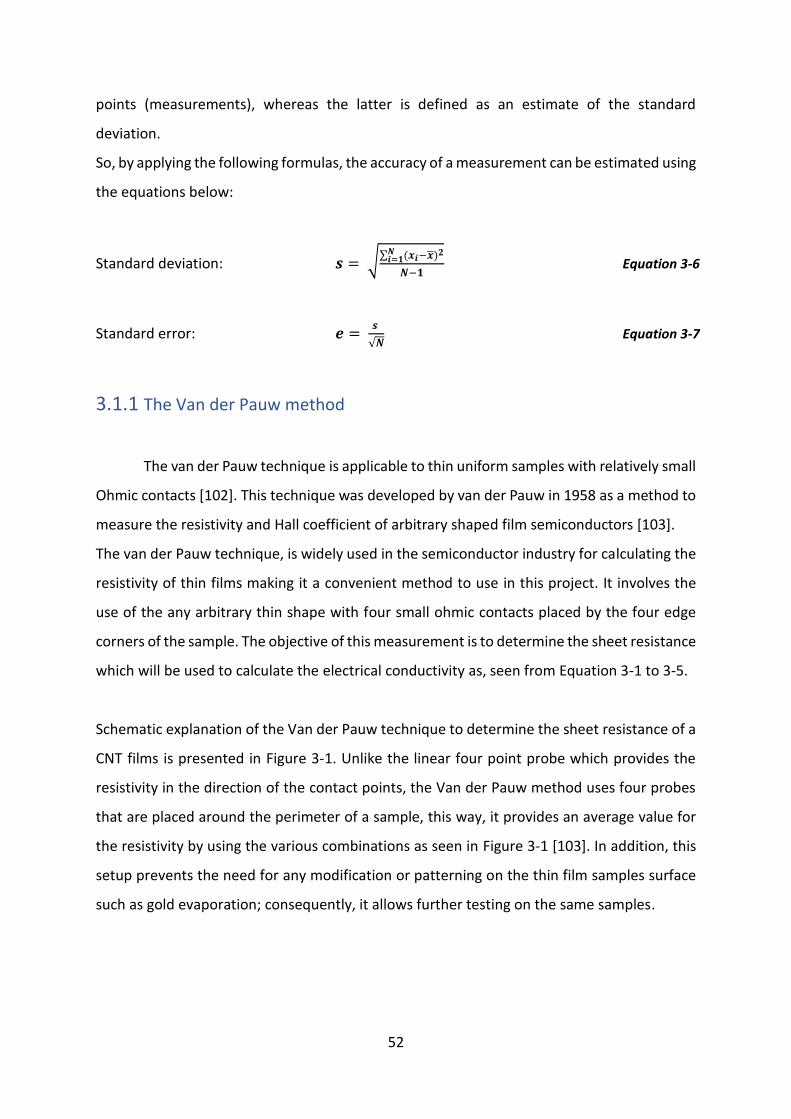
52
points (measurements), whereas the latter is defined as an estimate of the standard
deviation.
So, by applying the following formulas, the accuracy of a measurement can be estimated using
the equations below:
Standard deviation: 𝒔 = √∑ (𝒙𝒊−�̅�)𝟐𝑵
𝒊=𝟏
𝑵−𝟏 Equation 3-6
Standard error: 𝒆 = 𝒔
√𝑵 Equation 3-7
3.1.1 The Van der Pauw method
The van der Pauw technique is applicable to thin uniform samples with relatively small
Ohmic contacts [102]. This technique was developed by van der Pauw in 1958 as a method to
measure the resistivity and Hall coefficient of arbitrary shaped film semiconductors [103].
The van der Pauw technique, is widely used in the semiconductor industry for calculating the
resistivity of thin films making it a convenient method to use in this project. It involves the
use of the any arbitrary thin shape with four small ohmic contacts placed by the four edge
corners of the sample. The objective of this measurement is to determine the sheet resistance
which will be used to calculate the electrical conductivity as, seen from Equation 3-1 to 3-5.
Schematic explanation of the Van der Pauw technique to determine the sheet resistance of a
CNT films is presented in Figure 3-1. Unlike the linear four point probe which provides the
resistivity in the direction of the contact points, the Van der Pauw method uses four probes
that are placed around the perimeter of a sample, this way, it provides an average value for
the resistivity by using the various combinations as seen in Figure 3-1 [103]. In addition, this
setup prevents the need for any modification or patterning on the thin film samples surface
such as gold evaporation; consequently, it allows further testing on the same samples.
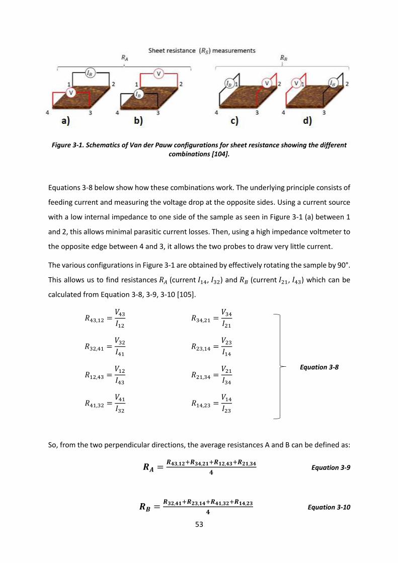
53
Figure 3-1. Schematics of Van der Pauw configurations for sheet resistance showing the different combinations [104].
Equations 3-8 below show how these combinations work. The underlying principle consists of
feeding current and measuring the voltage drop at the opposite sides. Using a current source
with a low internal impedance to one side of the sample as seen in Figure 3-1 (a) between 1
and 2, this allows minimal parasitic current losses. Then, using a high impedance voltmeter to
the opposite edge between 4 and 3, it allows the two probes to draw very little current.
The various configurations in Figure 3-1 are obtained by effectively rotating the sample by 90°.
This allows us to find resistances 𝑅𝐴 (current 𝐼14, 𝐼32) and 𝑅𝐵 (current 𝐼21, 𝐼43) which can be
calculated from Equation 3-8, 3-9, 3-10 [105].
𝑅43,12 =𝑉43
𝐼12 𝑅34,21 =
𝑉34
𝐼21
Equation 3-8
𝑅32,41 =𝑉32
𝐼41 𝑅23,14 =
𝑉23
𝐼14
𝑅12,43 =𝑉12
𝐼43 𝑅21,34 =
𝑉21
𝐼34
𝑅41,32 =𝑉41
𝐼32 𝑅14,23 =
𝑉14
𝐼23
So, from the two perpendicular directions, the average resistances A and B can be defined as:
𝑹𝑨 =𝑹𝟒𝟑,𝟏𝟐+𝑹𝟑𝟒,𝟐𝟏+𝑹𝟏𝟐,𝟒𝟑+𝑹𝟐𝟏,𝟑𝟒
𝟒 Equation 3-9
𝑹𝑩 =𝑹𝟑𝟐,𝟒𝟏+𝑹𝟐𝟑,𝟏𝟒+𝑹𝟒𝟏,𝟑𝟐+𝑹𝟏𝟒,𝟐𝟑
𝟒 Equation 3-10
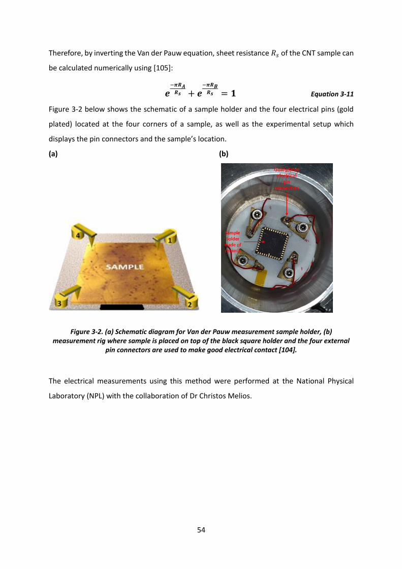
54
Therefore, by inverting the Van der Pauw equation, sheet resistance 𝑅𝑠 of the CNT sample can
be calculated numerically using [105]:
𝒆−𝝅𝑹𝑨
𝑹𝒔 + 𝒆−𝝅𝑹𝑩
𝑹𝒔 = 𝟏 Equation 3-11
Figure 3-2 below shows the schematic of a sample holder and the four electrical pins (gold
plated) located at the four corners of a sample, as well as the experimental setup which
displays the pin connectors and the sample’s location.
(a) (b)
Figure 3-2. (a) Schematic diagram for Van der Pauw measurement sample holder, (b) measurement rig where sample is placed on top of the black square holder and the four external
pin connectors are used to make good electrical contact [104].
The electrical measurements using this method were performed at the National Physical
Laboratory (NPL) with the collaboration of Dr Christos Melios.
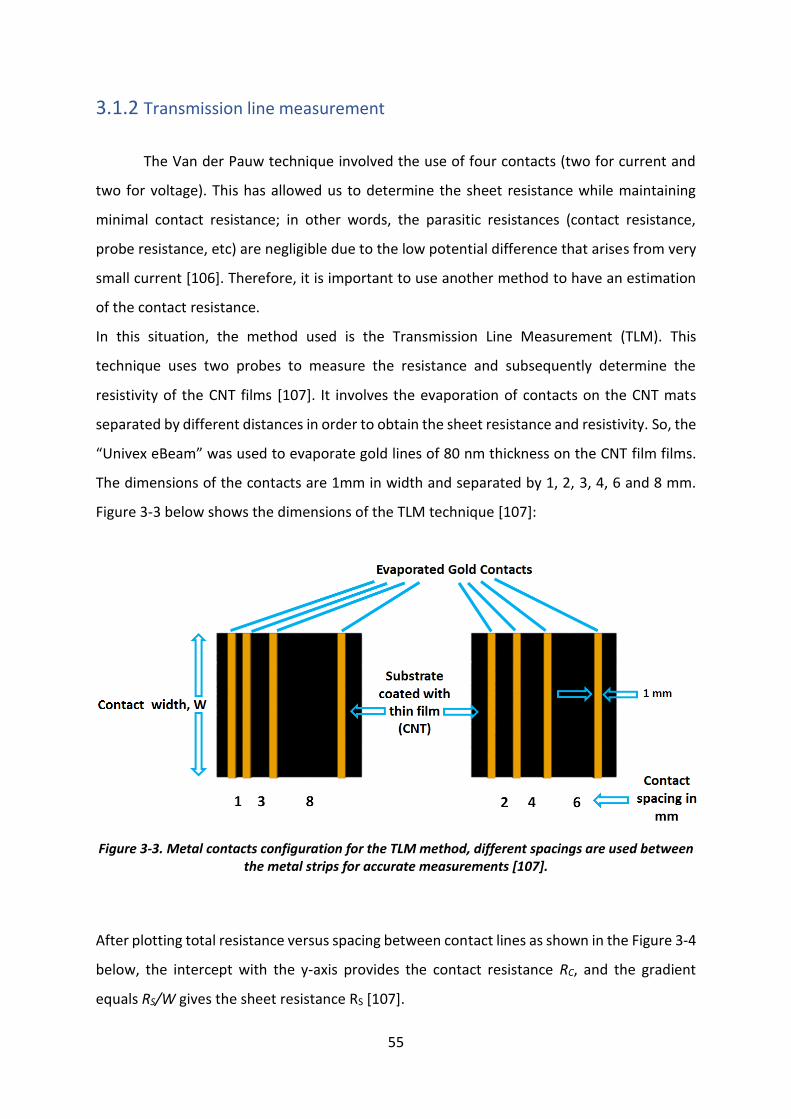
55
3.1.2 Transmission line measurement
The Van der Pauw technique involved the use of four contacts (two for current and
two for voltage). This has allowed us to determine the sheet resistance while maintaining
minimal contact resistance; in other words, the parasitic resistances (contact resistance,
probe resistance, etc) are negligible due to the low potential difference that arises from very
small current [106]. Therefore, it is important to use another method to have an estimation
of the contact resistance.
In this situation, the method used is the Transmission Line Measurement (TLM). This
technique uses two probes to measure the resistance and subsequently determine the
resistivity of the CNT films [107]. It involves the evaporation of contacts on the CNT mats
separated by different distances in order to obtain the sheet resistance and resistivity. So, the
“Univex eBeam” was used to evaporate gold lines of 80 nm thickness on the CNT film films.
The dimensions of the contacts are 1mm in width and separated by 1, 2, 3, 4, 6 and 8 mm.
Figure 3-3 below shows the dimensions of the TLM technique [107]:
Figure 3-3. Metal contacts configuration for the TLM method, different spacings are used between the metal strips for accurate measurements [107].
After plotting total resistance versus spacing between contact lines as shown in the Figure 3-4
below, the intercept with the y-axis provides the contact resistance RC, and the gradient
equals RS/W gives the sheet resistance RS [107].
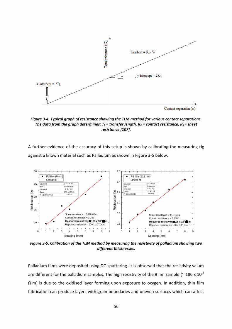
56
Figure 3-4. Typical graph of resistance showing the TLM method for various contact separations. The data from the graph determines: TL = transfer length, RC = contact resistance, RS = sheet
resistance [107].
A further evidence of the accuracy of this setup is shown by calibrating the measuring rig
against a known material such as Palladium as shown in Figure 3-5 below.
Figure 3-5. Calibration of the TLM method by measuring the resistivity of palladium showing two different thicknesses.
Palladium films were deposited using DC-sputtering. It is observed that the resistivity values
are different for the palladium samples. The high resistivity of the 9 nm sample (~ 186 x 10-9
Ω∙m) is due to the oxidised layer forming upon exposure to oxygen. In addition, thin film
fabrication can produce layers with grain boundaries and uneven surfaces which can affect
0 1 2 3 4 5 6 7 8 9
10
15
20
25
30
Sheet resistance = 2588 /sq
Contact resistance = 3.2
Measured resistivity 186 x 10-9 .m
Reported resistivity = 100 x 10-9 .m
Pd film (9 nm)
Linear fit
Resis
tance (
)
Spacing (mm)
Equation y = a + b*x
Plot Resistance
Intercept 6.4 ± 1.3
Slope 2.6k ± 289.9
R-Square(COD) 0.9522
0 1 2 3 4 5 6 7 8 9
0.6
0.8
1.0
1.2
1.4
1.6
Pd film (112 nm)
Linear fit
Re
sis
tance
(
)
Spacing (mm)
Equation y = a + b*x
Plot Resistance
Intercept 0.5 ± 0.0
Slope 117.4 ± 4.6
R-Square(COD) 0.99396
Sheet resistance = 117 /sq
Contact resistance = 0.25
Measured resistivity 105 x 10-9 .m
Reported resistivity = 100 x 10-9 .m
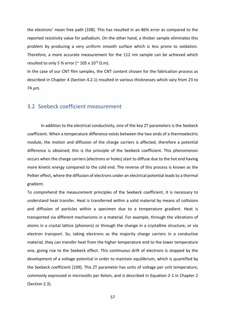
57
the electrons’ mean free path [108]. This has resulted in an 86% error as compared to the
reported resistivity value for palladium. On the other hand, a thicker sample eliminates this
problem by producing a very uniform smooth surface which is less prone to oxidation.
Therefore, a more accurate measurement for the 112 nm sample can be achieved which
resulted to only 5 % error (~ 105 x 10-9 Ω.m).
In the case of our CNT film samples, the CNT content chosen for the fabrication process as
described in Chapter 4 (Section 4.2.1) resulted in various thicknesses which vary from 23 to
74 µm.
3.2 Seebeck coefficient measurement
In addition to the electrical conductivity, one of the key ZT parameters is the Seebeck
coefficient. When a temperature difference exists between the two ends of a thermoelectric
module, the motion and diffusion of the charge carriers is affected, therefore a potential
difference is obtained; this is the principle of the Seebeck coefficient. This phenomenon
occurs when the charge carriers (electrons or holes) start to diffuse due to the hot end having
more kinetic energy compared to the cold end. The reverse of this process is known as the
Peltier effect, where the diffusion of electrons under an electrical potential leads to a thermal
gradient.
To comprehend the measurement principles of the Seebeck coefficient, it is necessary to
understand heat transfer. Heat is transferred within a solid material by means of collisions
and diffusion of particles within a specimen due to a temperature gradient. Heat is
transported via different mechanisms in a material. For example, through the vibrations of
atoms in a crystal lattice (phonons) or through the change in a crystalline structure, or via
electron transport. So, taking electrons as the majority charge carriers in a conductive
material, they can transfer heat from the higher temperature end to the lower temperature
one, giving rise to the Seebeck effect. This continuous drift of electrons is stopped by the
development of a voltage potential in order to maintain equilibrium, which is quantified by
the Seebeck coefficient [109]. This ZT parameter has units of voltage per unit temperature,
commonly expressed in microvolts per Kelvin, and is described in Equation 2-1 in Chapter 2
(Section 2.3).
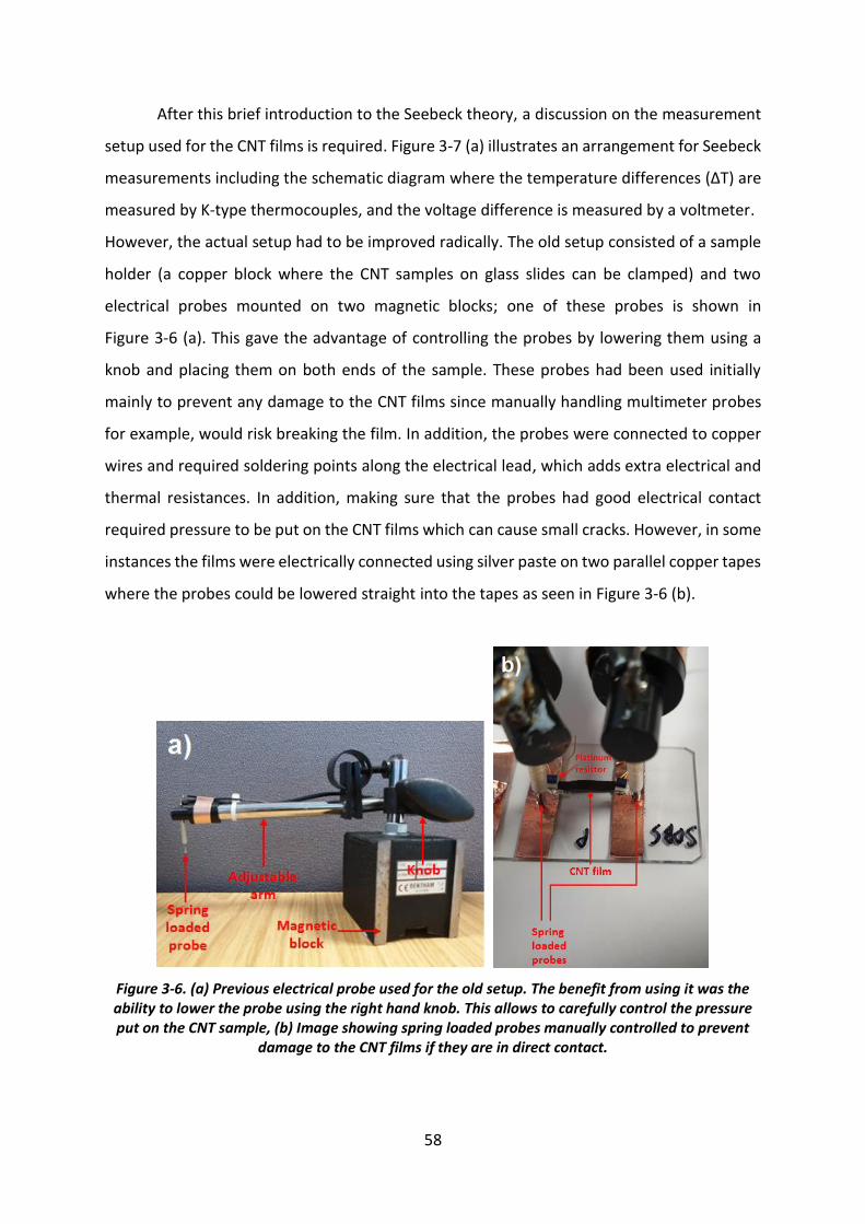
58
After this brief introduction to the Seebeck theory, a discussion on the measurement
setup used for the CNT films is required. Figure 3-7 (a) illustrates an arrangement for Seebeck
measurements including the schematic diagram where the temperature differences (ΔT) are
measured by K-type thermocouples, and the voltage difference is measured by a voltmeter.
However, the actual setup had to be improved radically. The old setup consisted of a sample
holder (a copper block where the CNT samples on glass slides can be clamped) and two
electrical probes mounted on two magnetic blocks; one of these probes is shown in
Figure 3-6 (a). This gave the advantage of controlling the probes by lowering them using a
knob and placing them on both ends of the sample. These probes had been used initially
mainly to prevent any damage to the CNT films since manually handling multimeter probes
for example, would risk breaking the film. In addition, the probes were connected to copper
wires and required soldering points along the electrical lead, which adds extra electrical and
thermal resistances. In addition, making sure that the probes had good electrical contact
required pressure to be put on the CNT films which can cause small cracks. However, in some
instances the films were electrically connected using silver paste on two parallel copper tapes
where the probes could be lowered straight into the tapes as seen in Figure 3-6 (b).
Figure 3-6. (a) Previous electrical probe used for the old setup. The benefit from using it was the ability to lower the probe using the right hand knob. This allows to carefully control the pressure put on the CNT sample, (b) Image showing spring loaded probes manually controlled to prevent
damage to the CNT films if they are in direct contact.
59
One of the issues to overcome when measuring the Seebeck coefficient is thermal resistance.
It is defined as the resistance of a material to the heat flow at the junction between the
electrical contacts and the samples. In contrast, thermal conductivity is a material’s property
which describes its ability to conduct heat. Thermal conductance is comparable to electrical
resistance. The latter is the potential difference between two points divided by the current
flowing across them. Thus, it can be concluded that there are similarities between voltage
and temperature and current and heat transfer. In essence, a voltage difference is generated
as a result to electrical conduction, whereas thermal conduction occurs as a consequence of
a temperature difference.
Thermal contact stability at the interface between the hot source and the CNT films is key to
improving the performance of the TE device. Since most surfaces including the CNT films used
are not perfectly smooth, there will be an air gap between the samples and the heat source.
Additionally, a thermal contact resistance is generated because of the large difference
between the thermal conductivity values of both air and samples which causes a contraction
of the heat flow [110]. Therefore, the output power will decrease due to the existence of the
thermal resistance which reduces the temperature gradient between the hot and cold side.
It has been reported in a previous study [111] that eliminating air gaps at the interface can be
achieved by using thermal grease which contributes to decreasing the contact resistance.
After reviewing all the potential issues that can arise for the Seebeck measurements, various
improvements were done in order to obtain near accurate data as seen in the new schematic
setup shown in Figure 3-7 (a). First of all, the measurements were performed in vacuum,
which can help in reducing thermal losses. For the preparation of the samples, silver epoxy
was used at the interface. The kit consists of both the resin (silver paste) and the hardener
(cure); the ideal mixture was 1:1 ratio. The curing time was 24 h at 25 °C or 20 - 30 min @
100 °C. The thermal conductivity value for this material is around 11 W/m.K. In addition to
using a highly conductive material to guarantee both thermal and electrical contact a glove
box was used in order to prevent oxygen from being trapped at the interface (silver epoxy
and CNT film), thus minimising thermal resistance. Also, for each sample measured, the
electrodes were soldered onto the copper tapes which will ensure an ohmic contact. Whereas
the thermocouples were covered by copper tape to reduce thermal loss.
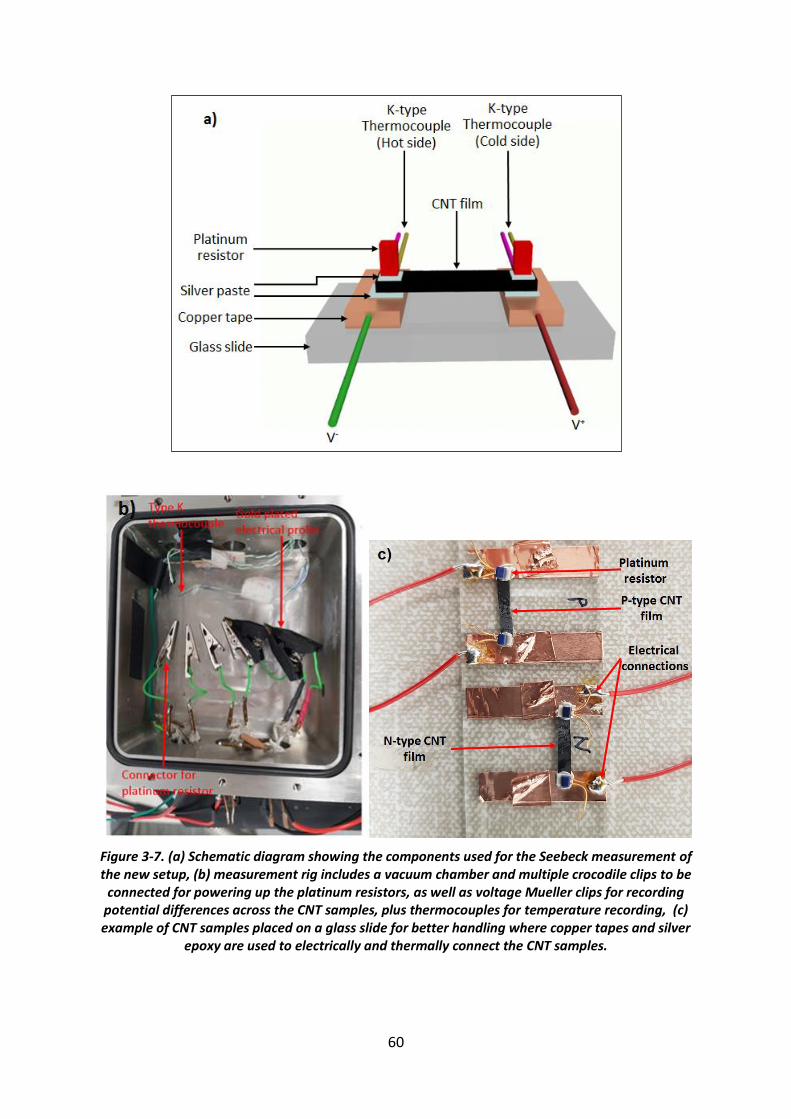
60
Figure 3-7. (a) Schematic diagram showing the components used for the Seebeck measurement of the new setup, (b) measurement rig includes a vacuum chamber and multiple crocodile clips to be
connected for powering up the platinum resistors, as well as voltage Mueller clips for recording potential differences across the CNT samples, plus thermocouples for temperature recording, (c) example of CNT samples placed on a glass slide for better handling where copper tapes and silver
epoxy are used to electrically and thermally connect the CNT samples.
61
In this project, for ease of handling and due to the fragility of the CNT films, the samples were
placed on a glass substrate positioned between two conducting copper tapes as seen in
Figure 3-7 (c). Another reason for choosing a glass slide is its low thermal conductivity which
is ~ 1 W/mK. This makes heat transfer from the hot side to the cold side extremely slow, thus
preventing any negative influence on the cold side.
One end of the sample is heated with a platinum resistor (set at a higher voltage) acting as an
active heater while the other end which acts as a heat sink was also connected to another
platinum resistor (set at lower voltage); this is to create a linear temperature gradient across
the film. This renders the CNT sample to go through a drift phase where the charge carriers
are thermally excited and drawn to the cold side, followed by a steady state. Therefore,
before collecting any data, the system must be in a steady state which takes around 480
seconds making the overall acquisition time to 500 seconds for each temperature difference
as seen in Figure 3-8. The linearity is particularly important because the Seebeck coefficient
is highly dependent on temperature change; the charge carriers’ diffusion from the hot end
to the cold end varies depending on the temperature difference across the CNT films.
Therefore, to obtain a constant Seebeck coefficient, the measurements were carried out
using the Keysight B2902A where the potential difference was computed across the samples
at five temperature gradients within a small range from 7 to 18 ˚C (ΔT1 to ΔT2). To reduce the
need for recovery time, all measurements were performed from a low temperature
difference to a high temperature difference, after reaching steady state. The cold side
temperature does increase over this period, reaching a maximum increase of ~ 3-4 ˚C; this is
small compared to the highest temperature difference (35 - 40 ˚C) and more accurate
readings would require active cooling, which would make the design much more complex (i.e.
by adding a Peltier cooler); as a good linear behaviour was observed at higher temperature
differences in Figure 3-9, this was not deemed necessary at this stage. This is only applicable
to these CNT films, and another material is likely to require active cooling. On the other hand,
Thermocouples were placed on the copper tapes in close proximity to the platinum resistors
and were covered with small copper tape. The thermocouples are used to register the
temperature differences and were measured using the Pico Data Logger TC-08 which has 8
input channels with a high 20-bit resolution ensuring that the kit can detect near instant
temperature changes. In addition, for K-type thermocouples, the TC-08 can maintain a
62
0.025 ˚C resolution over a wide temperature range (-250 to +1370 ˚C) according to its data
sheet [112].
Figure 3-8. Data shows the temperature differences (ΔT1 to ΔT5) for p-type Pluronic F127/CNT within a range varying between 7 to 18 ˚C acquired using the Pico Data Logger TC-08. The steady
state is reached after ~ 480 Seconds.
To further understand the difference between the “Old setup” and the “New setup”, a
calibration of both systems was needed to highlight the measurement setbacks that can be
encountered. Two materials were chosen for this calibration, nickel (Ni) and n-type silicon
(Si). The improved setup is referred to as “New setup” which is shown in Figure 3-7 above.
The previous setup which was used as a reference method to make improvements in the
measurements is referred to as “Old setup”. Figure 3-9 shows the data obtained for the two
setups.
0 100 200 300 400 500 600
0
2
4
6
8
10
12
14
16
18
20
Drift
state
Tem
pera
ture
diffe
rence (C
)
Time (S)
Steady
state
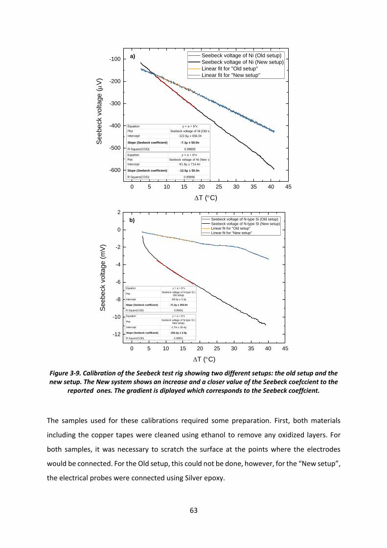
63
Figure 3-9. Calibration of the Seebeck test rig showing two different setups: the old setup and the new setup. The New system shows an increase and a closer value of the Seebeck coefccient to the
reported ones. The gradient is diplayed which corresponds to the Seebeck coeffcient.
The samples used for these calibrations required some preparation. First, both materials
including the copper tapes were cleaned using ethanol to remove any oxidized layers. For
both samples, it was necessary to scratch the surface at the points where the electrodes
would be connected. For the Old setup, this could not be done, however, for the “New setup”,
the electrical probes were connected using Silver epoxy.
0 5 10 15 20 25 30 35 40 45
-600
-500
-400
-300
-200
-100
Seebeck v
oltage (
V)
T (C)
Seebeck voltage of Ni (Old setup)
Seebeck voltage of Ni (New setup)
Linear fit for "Old setup"
Linear fit for "New setup"
Equation y = a + b*x
Plot Seebeck voltage of Ni (New s
Intercept -91.9µ ± 714.4n
Slope (Seebeck coefficient) -12.5µ ± 55.0n
R-Square(COD) 0.99896
Equation y = a + b*x
Plot Seebeck voltage of Ni (Old s
Intercept -122.6µ ± 656.0n
Slope (Seebeck coefficient) -7.1µ ± 50.0n
R-Square(COD) 0.98859
a)
0 5 10 15 20 25 30 35 40 45
-12
-10
-8
-6
-4
-2
0
2
See
be
ck v
olta
ge
(m
V)
T (C)
Seebeck voltage of N-type Si (Old setup)
Seebeck voltage of N-type SI (New setup)
Linear fit for "Old setup"
Linear fit for "New setup"
Equation y = a + b*x
PlotSeebeck voltage of N-type SI (
New setup)
Intercept -1.7m ± 26.4µ
Slope (Seebeck coefficient) -252.2µ ± 2.0µ
R-Square(COD) 0.99551
Equation y = a + b*x
PlotSeebeck voltage of N-type Si (
Old setup)
Intercept -69.5µ ± 3.3µ
Slope (Seebeck coefficient) -71.2µ ± 254.0n
R-Square(COD) 0.99591
b)
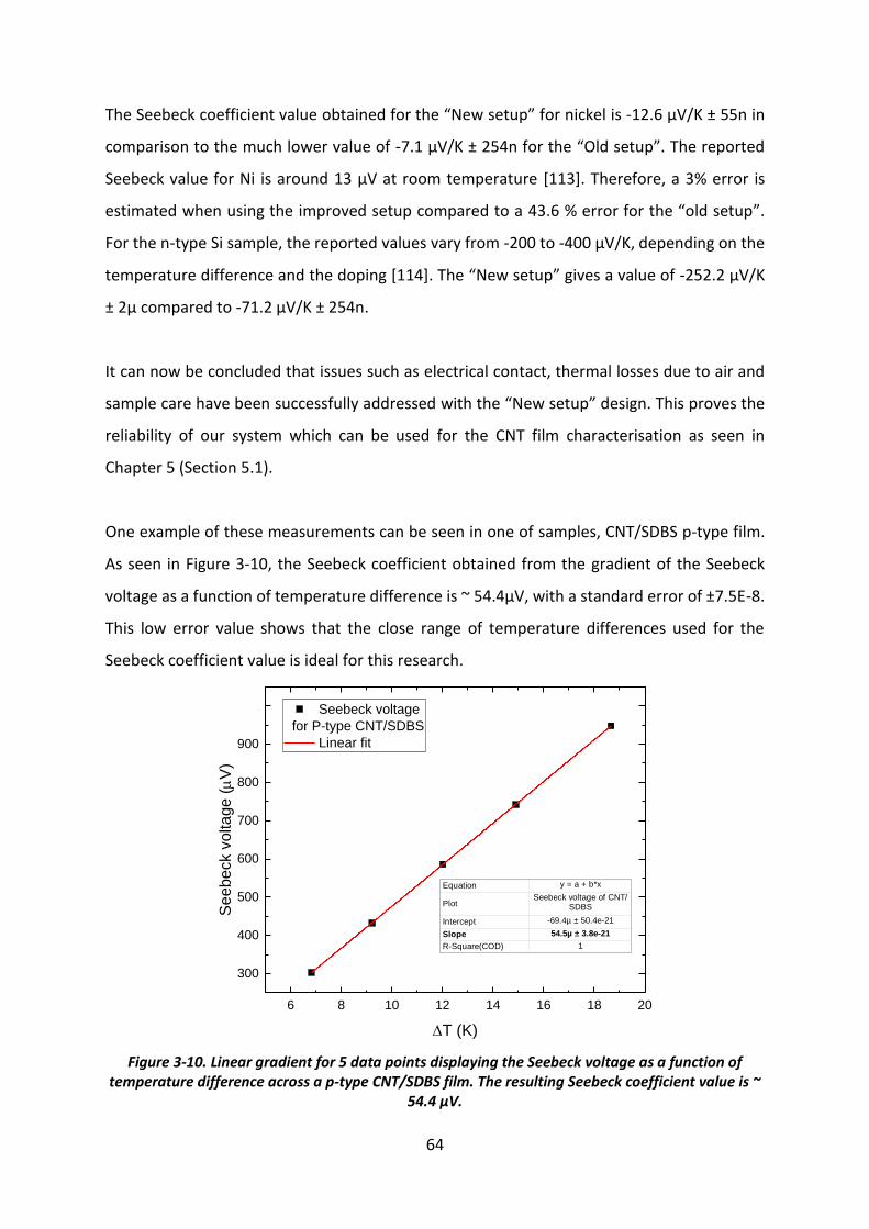
64
The Seebeck coefficient value obtained for the “New setup” for nickel is -12.6 µV/K ± 55n in
comparison to the much lower value of -7.1 µV/K ± 254n for the “Old setup”. The reported
Seebeck value for Ni is around 13 µV at room temperature [113]. Therefore, a 3% error is
estimated when using the improved setup compared to a 43.6 % error for the “old setup”.
For the n-type Si sample, the reported values vary from -200 to -400 µV/K, depending on the
temperature difference and the doping [114]. The “New setup” gives a value of -252.2 µV/K
± 2µ compared to -71.2 µV/K ± 254n.
It can now be concluded that issues such as electrical contact, thermal losses due to air and
sample care have been successfully addressed with the “New setup” design. This proves the
reliability of our system which can be used for the CNT film characterisation as seen in
Chapter 5 (Section 5.1).
One example of these measurements can be seen in one of samples, CNT/SDBS p-type film.
As seen in Figure 3-10, the Seebeck coefficient obtained from the gradient of the Seebeck
voltage as a function of temperature difference is ~ 54.4µV, with a standard error of ±7.5E-8.
This low error value shows that the close range of temperature differences used for the
Seebeck coefficient value is ideal for this research.
Figure 3-10. Linear gradient for 5 data points displaying the Seebeck voltage as a function of temperature difference across a p-type CNT/SDBS film. The resulting Seebeck coefficient value is ~
54.4 µV.
6 8 10 12 14 16 18 20
300
400
500
600
700
800
900
1k Seebeck voltage
for P-type CNT/SDBS
Linear fit
Se
ebe
ck v
olta
ge
(
V)
T (K)
Equation y = a + b*x
PlotSeebeck voltage of CNT/
SDBS
Intercept -69.4µ ± 50.4e-21
Slope 54.5µ ± 3.8e-21
R-Square(COD) 1
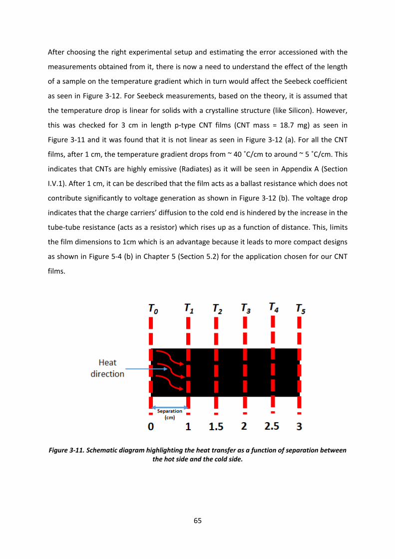
65
After choosing the right experimental setup and estimating the error accessioned with the
measurements obtained from it, there is now a need to understand the effect of the length
of a sample on the temperature gradient which in turn would affect the Seebeck coefficient
as seen in Figure 3-12. For Seebeck measurements, based on the theory, it is assumed that
the temperature drop is linear for solids with a crystalline structure (like Silicon). However,
this was checked for 3 cm in length p-type CNT films (CNT mass = 18.7 mg) as seen in
Figure 3-11 and it was found that it is not linear as seen in Figure 3-12 (a). For all the CNT
films, after 1 cm, the temperature gradient drops from ~ 40 ˚C/cm to around ~ 5 ˚C/cm. This
indicates that CNTs are highly emissive (Radiates) as it will be seen in Appendix A (Section
I.V.1). After 1 cm, it can be described that the film acts as a ballast resistance which does not
contribute significantly to voltage generation as shown in Figure 3-12 (b). The voltage drop
indicates that the charge carriers’ diffusion to the cold end is hindered by the increase in the
tube-tube resistance (acts as a resistor) which rises up as a function of distance. This, limits
the film dimensions to 1cm which is an advantage because it leads to more compact designs
as shown in Figure 5-4 (b) in Chapter 5 (Section 5.2) for the application chosen for our CNT
films.
Figure 3-11. Schematic diagram highlighting the heat transfer as a function of separation between the hot side and the cold side.
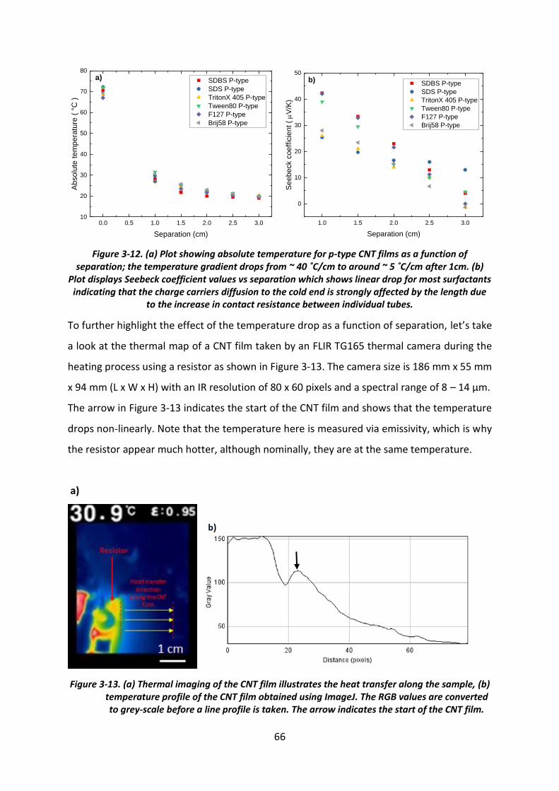
66
Figure 3-12. (a) Plot showing absolute temperature for p-type CNT films as a function of separation; the temperature gradient drops from ~ 40 ˚C/cm to around ~ 5 ˚C/cm after 1cm. (b)
Plot displays Seebeck coefficient values vs separation which shows linear drop for most surfactants indicating that the charge carriers diffusion to the cold end is strongly affected by the length due
to the increase in contact resistance between individual tubes.
To further highlight the effect of the temperature drop as a function of separation, let’s take
a look at the thermal map of a CNT film taken by an FLIR TG165 thermal camera during the
heating process using a resistor as shown in Figure 3-13. The camera size is 186 mm x 55 mm
x 94 mm (L x W x H) with an IR resolution of 80 x 60 pixels and a spectral range of 8 – 14 µm.
The arrow in Figure 3-13 indicates the start of the CNT film and shows that the temperature
drops non-linearly. Note that the temperature here is measured via emissivity, which is why
the resistor appear much hotter, although nominally, they are at the same temperature.
a)
Figure 3-13. (a) Thermal imaging of the CNT film illustrates the heat transfer along the sample, (b) temperature profile of the CNT film obtained using ImageJ. The RGB values are converted to grey-scale before a line profile is taken. The arrow indicates the start of the CNT film.
0.0 0.5 1.0 1.5 2.0 2.5 3.010
20
30
40
50
60
70
80
SDBS P-type
SDS P-type
TritonX 405 P-type
Tween80 P-type
F127 P-type
Brij58 P-type
Ab
so
lute
te
mp
era
ture
( °
C )
Separation (cm)
a)
1.0 1.5 2.0 2.5 3.0
0
10
20
30
40
50
SDBS P-type
SDS P-type
TritonX 405 P-type
Tween80 P-type
F127 P-type
Brij58 P-type
Se
ebe
ck c
oe
ffic
ien
t (
V/K
)
Separation (cm)
b)
67
3.3 Scanning Electron Microscopy
To analyse the characteristics of the CNTs within the films, a small cut was made in
order to inspect the uniformity of the films and to review the height of individual CNTs. This
analysis was performed using scanning electron microscopy (SEM). It is a technique used to
measure the height of the vertically aligned CNTs (VACNTs) on a silicon wafer and the
thickness of the CNT films. It is a quick and non-destructive imaging method conducted in a
vacuum environment [115]. In high vacuum, a better resolution can be obtained due to the
low scattering between the electrons beam and the gas atoms. Using a focused beam of
electrons from a gun, these electrons are then accelerated through a condenser lens where
they are converged using electromagnetic coils. Next, with an objective lens, the beam is
focused onto a particular area of a sample. To allow movement in the x and y direction, scan
coils present between the condenser and objective lenses use electrostatic fields to direct the
beam. Once the incident electron strikes the surface of a sample, an elastic or inelastic
scattering occurs resulting in: secondary electron emission, back-scattered electron emission,
Auger electron emission and X-ray emission. Secondary electron emission is used for
morphology analysis. This secondary electron interacts with the detector resulting in an image
where the topography and morphology of the sample can be assessed. An example of a CNT
film’s small section is shown below in Figure 3-14 (a).
In this project, the samples were placed on a sample holder positioned at a 90˚angle to the
viewing direction in order to obtain a visualisation of the uniformity of the film and the CNTs.
The sample holder on a metallic stub was covered by carbon tape to keep the sample stable.
The chamber is then shut and pumped down to a vacuum of ≤ 1 × 10⁻⁴ mbar. The SEM
apparatus used for obtaining images is the FEI Quanta ESEM. The accelerating voltage was
varied from 5 kV to 30 kV and a spot size from 3.0 to 4.0 depending on the sample. The
increase in the accelerating voltage rises up the incident beam of electrons, resulting in a
smaller beam spot which can improve resolution. The images obtained were analysed using
“ImageJ” software for assessing the height of VACNTs and thickness of CNT films.
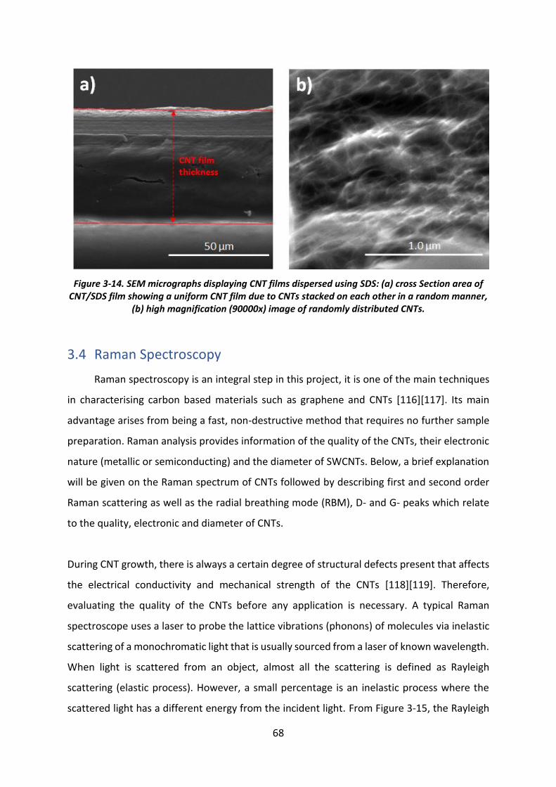
68
Figure 3-14. SEM micrographs displaying CNT films dispersed using SDS: (a) cross Section area of CNT/SDS film showing a uniform CNT film due to CNTs stacked on each other in a random manner,
(b) high magnification (90000x) image of randomly distributed CNTs.
3.4 Raman Spectroscopy
Raman spectroscopy is an integral step in this project, it is one of the main techniques
in characterising carbon based materials such as graphene and CNTs [116][117]. Its main
advantage arises from being a fast, non-destructive method that requires no further sample
preparation. Raman analysis provides information of the quality of the CNTs, their electronic
nature (metallic or semiconducting) and the diameter of SWCNTs. Below, a brief explanation
will be given on the Raman spectrum of CNTs followed by describing first and second order
Raman scattering as well as the radial breathing mode (RBM), D- and G- peaks which relate
to the quality, electronic and diameter of CNTs.
During CNT growth, there is always a certain degree of structural defects present that affects
the electrical conductivity and mechanical strength of the CNTs [118][119]. Therefore,
evaluating the quality of the CNTs before any application is necessary. A typical Raman
spectroscope uses a laser to probe the lattice vibrations (phonons) of molecules via inelastic
scattering of a monochromatic light that is usually sourced from a laser of known wavelength.
When light is scattered from an object, almost all the scattering is defined as Rayleigh
scattering (elastic process). However, a small percentage is an inelastic process where the
scattered light has a different energy from the incident light. From Figure 3-15, the Rayleigh
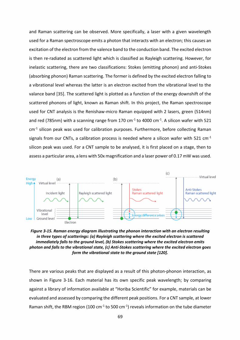
69
and Raman scattering can be observed. More specifically, a laser with a given wavelength
used for a Raman spectroscope emits a photon that interacts with an electron; this causes an
excitation of the electron from the valence band to the conduction band. The excited electron
is then re-radiated as scattered light which is classified as Rayleigh scattering. However, for
inelastic scattering, there are two classifications: Stokes (emitting phonon) and anti-Stokes
(absorbing phonon) Raman scattering. The former is defined by the excited electron falling to
a vibrational level whereas the latter is an electron excited from the vibrational level to the
valance band [35]. The scattered light is plotted as a function of the energy downshift of the
scattered phonons of light, known as Raman shift. In this project, the Raman spectroscope
used for CNT analysis is the Renishaw-micro Raman equipped with 2 lasers, green (514nm)
and red (785nm) with a scanning range from 170 cm-1 to 4000 cm-1. A silicon wafer with 521
cm-1 silicon peak was used for calibration purposes. Furthermore, before collecting Raman
signals from our CNTs, a calibration process is needed where a silicon wafer with 521 cm-1
silicon peak was used. For a CNT sample to be analysed, it is first placed on a stage, then to
assess a particular area, a lens with 50x magnification and a laser power of 0.17 mW was used.
Figure 3-15. Raman energy diagram illustrating the phonon interaction with an electron resulting in three types of scatterings: (a) Rayleigh scattering where the excited electron is scattered immediately falls to the ground level, (b) Stokes scattering where the excited electron emits
photon and falls to the vibrational state, (c) Anti-Stokes scattering where the excited electron goes form the vibrational state to the ground state [120].
There are various peaks that are displayed as a result of this photon-phonon interaction, as
shown in Figure 3-16. Each material has its own specific peak wavelength; by comparing
against a library of information available at “Horiba Scientific” for example, materials can be
evaluated and assessed by comparing the different peak positions. For a CNT sample, at lower
Raman shift, the RBM region (100 cm-1 to 500 cm-1) reveals information on the tube diameter
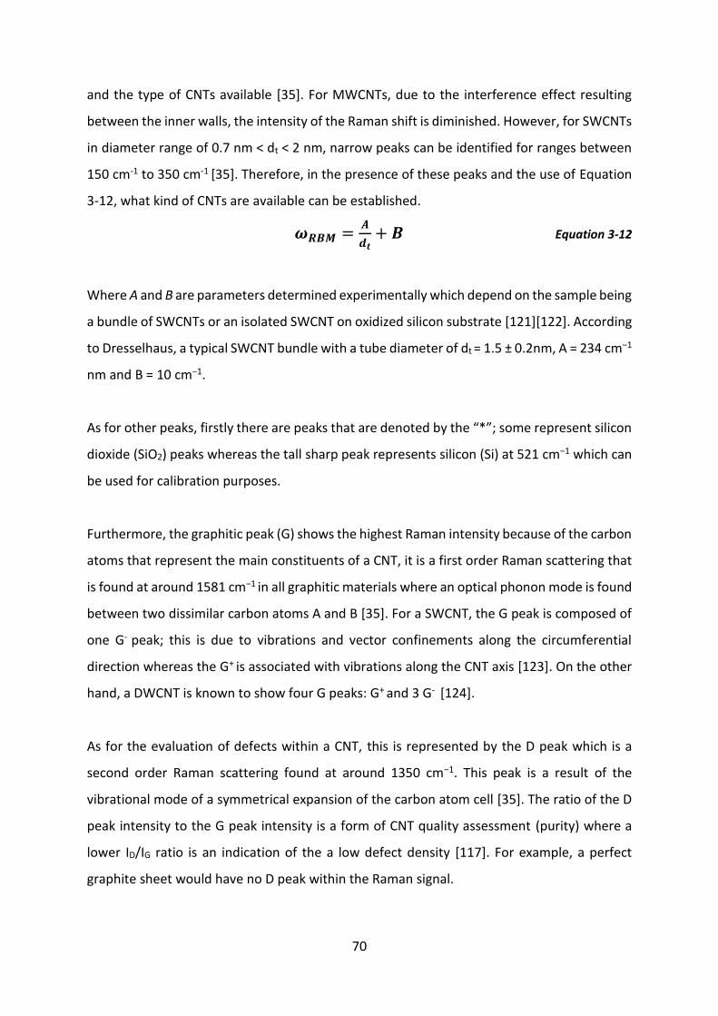
70
and the type of CNTs available [35]. For MWCNTs, due to the interference effect resulting
between the inner walls, the intensity of the Raman shift is diminished. However, for SWCNTs
in diameter range of 0.7 nm < dt < 2 nm, narrow peaks can be identified for ranges between
150 cm-1 to 350 cm-1 [35]. Therefore, in the presence of these peaks and the use of Equation
3-12, what kind of CNTs are available can be established.
𝝎𝑹𝑩𝑴 =𝑨
𝒅𝒕+ 𝑩 Equation 3-12
Where A and B are parameters determined experimentally which depend on the sample being
a bundle of SWCNTs or an isolated SWCNT on oxidized silicon substrate [121][122]. According
to Dresselhaus, a typical SWCNT bundle with a tube diameter of dt = 1.5 ± 0.2nm, A = 234 cm−1
nm and B = 10 cm−1.
As for other peaks, firstly there are peaks that are denoted by the “*”; some represent silicon
dioxide (SiO2) peaks whereas the tall sharp peak represents silicon (Si) at 521 cm−1 which can
be used for calibration purposes.
Furthermore, the graphitic peak (G) shows the highest Raman intensity because of the carbon
atoms that represent the main constituents of a CNT, it is a first order Raman scattering that
is found at around 1581 cm−1 in all graphitic materials where an optical phonon mode is found
between two dissimilar carbon atoms A and B [35]. For a SWCNT, the G peak is composed of
one G- peak; this is due to vibrations and vector confinements along the circumferential
direction whereas the G+ is associated with vibrations along the CNT axis [123]. On the other
hand, a DWCNT is known to show four G peaks: G+ and 3 G- [124].
As for the evaluation of defects within a CNT, this is represented by the D peak which is a
second order Raman scattering found at around 1350 cm−1. This peak is a result of the
vibrational mode of a symmetrical expansion of the carbon atom cell [35]. The ratio of the D
peak intensity to the G peak intensity is a form of CNT quality assessment (purity) where a
lower ID/IG ratio is an indication of the a low defect density [117]. For example, a perfect
graphite sheet would have no D peak within the Raman signal.
71
The M-band, found at around 1750 cm−1 is related to multiple layer CNTs such as DWCNTs
and MWCNTs which is defined as a combination of vibrational modes in the second order
overtone. Another peak known as the iTOLA is attributed to the combinational modes of the
in-plane transverse longitudinal acoustic (L(A) mode and longitudinal optical (LO) mode [125].
Finally, the 2D peak which is the second most intense peak after the G-band. This peak is
considered an overtone to the D-band, which is referred to as the G´ in Figure 3-16. This
number “2” associated to it is in reference to its double frequency shift of the original D peak.
Figure 3-16. SWCNT Raman signals displaying various peaks: RBM region for determining CNT diameter, Silicon peak used as a reference point, D peak corresponds to the defective sites within
the CNTs, G peak related to the graphitic content of CNTs [35].
The peak discussed above can be found in one of the samples that was measured using our
Raman system as shown in Figure 3-17. This particular CNTs were purshased from Sigma
Aldrich (product code: 773735) and were characterised for the purpose of comparison with
the peaks observed in Figure 3-16. Their high quality can be seen form the ID/IG ratio which
was calcualted to be ~ 0.06. This high purity can be attributed to the high temperature process
(˃ 700 ˚C) used during the growth which consists of a silica supported catalyst CVD method
(CoMoCAT CVD). The resulting CNTs have an avreage diameter of 0.78 nm with
semiconducting composition of approximately 95% according to the data sheet [126].
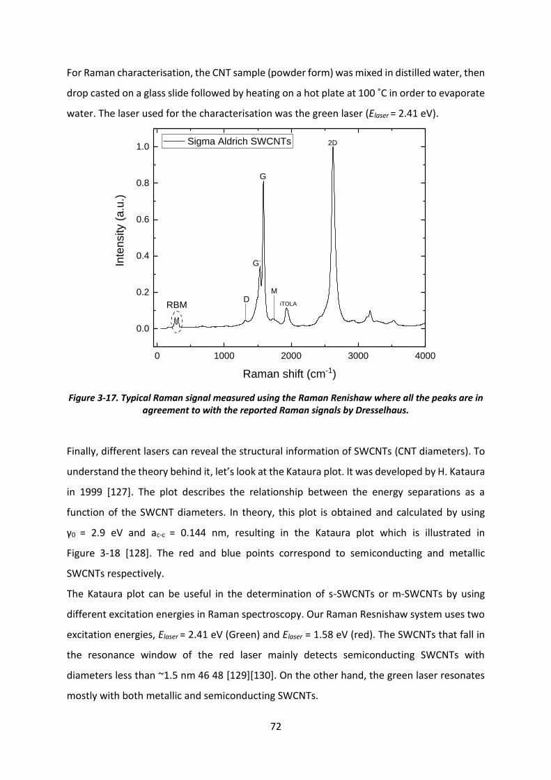
72
For Raman characterisation, the CNT sample (powder form) was mixed in distilled water, then
drop casted on a glass slide followed by heating on a hot plate at 100 ˚C in order to evaporate
water. The laser used for the characterisation was the green laser (Elaser = 2.41 eV).
Figure 3-17. Typical Raman signal measured using the Raman Renishaw where all the peaks are in agreement to with the reported Raman signals by Dresselhaus.
Finally, different lasers can reveal the structural information of SWCNTs (CNT diameters). To
understand the theory behind it, let’s look at the Kataura plot. It was developed by H. Kataura
in 1999 [127]. The plot describes the relationship between the energy separations as a
function of the SWCNT diameters. In theory, this plot is obtained and calculated by using
γ0 = 2.9 eV and ac-c = 0.144 nm, resulting in the Kataura plot which is illustrated in
Figure 3-18 [128]. The red and blue points correspond to semiconducting and metallic
SWCNTs respectively.
The Kataura plot can be useful in the determination of s-SWCNTs or m-SWCNTs by using
different excitation energies in Raman spectroscopy. Our Raman Resnishaw system uses two
excitation energies, Elaser = 2.41 eV (Green) and Elaser = 1.58 eV (red). The SWCNTs that fall in
the resonance window of the red laser mainly detects semiconducting SWCNTs with
diameters less than ~1.5 nm 46 48 [129][130]. On the other hand, the green laser resonates
mostly with both metallic and semiconducting SWCNTs.
0 1000 2000 3000 4000
0.0
0.2
0.4
0.6
0.8
1.02D
iTOLA
MD
G
G-
RBM
Inte
nsity (
a.u
.)
Raman shift (cm-1)
Sigma Aldrich SWCNTs
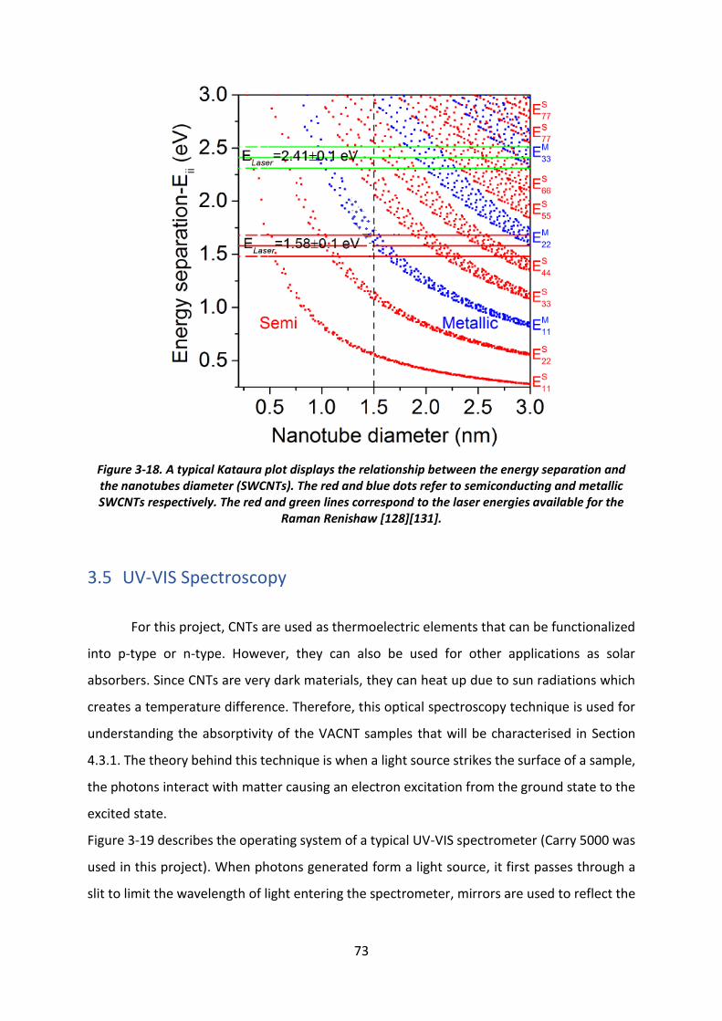
73
Figure 3-18. A typical Kataura plot displays the relationship between the energy separation and the nanotubes diameter (SWCNTs). The red and blue dots refer to semiconducting and metallic SWCNTs respectively. The red and green lines correspond to the laser energies available for the
Raman Renishaw [128][131].
3.5 UV-VIS Spectroscopy
For this project, CNTs are used as thermoelectric elements that can be functionalized
into p-type or n-type. However, they can also be used for other applications as solar
absorbers. Since CNTs are very dark materials, they can heat up due to sun radiations which
creates a temperature difference. Therefore, this optical spectroscopy technique is used for
understanding the absorptivity of the VACNT samples that will be characterised in Section
4.3.1. The theory behind this technique is when a light source strikes the surface of a sample,
the photons interact with matter causing an electron excitation from the ground state to the
excited state.
Figure 3-19 describes the operating system of a typical UV-VIS spectrometer (Carry 5000 was
used in this project). When photons generated form a light source, it first passes through a
slit to limit the wavelength of light entering the spectrometer, mirrors are used to reflect the
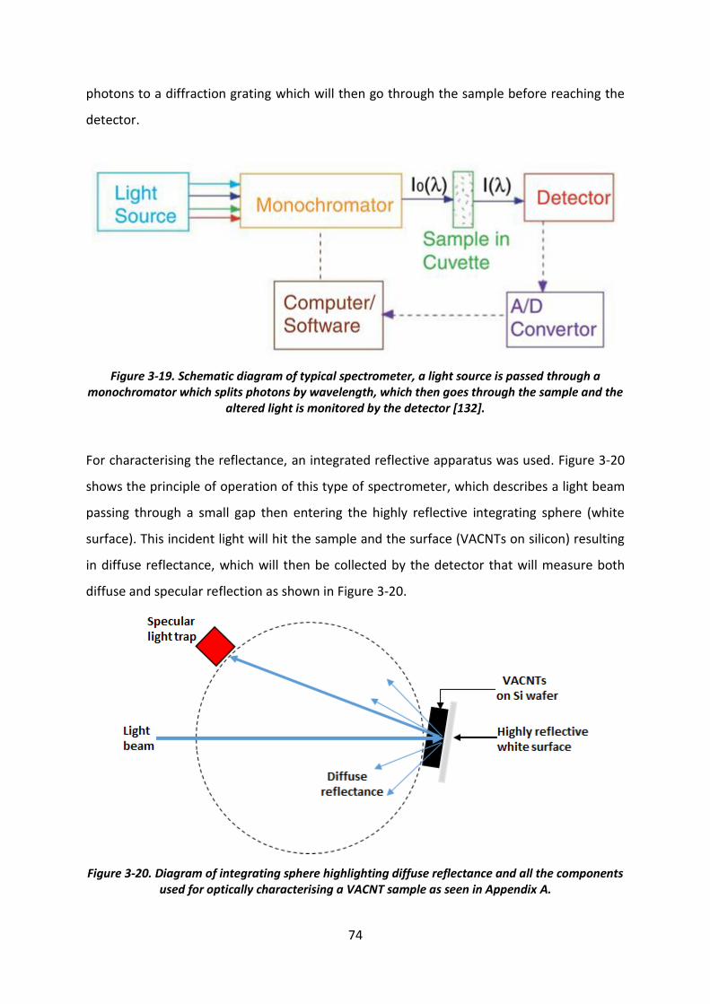
74
photons to a diffraction grating which will then go through the sample before reaching the
detector.
Figure 3-19. Schematic diagram of typical spectrometer, a light source is passed through a monochromator which splits photons by wavelength, which then goes through the sample and the
altered light is monitored by the detector [132].
For characterising the reflectance, an integrated reflective apparatus was used. Figure 3-20
shows the principle of operation of this type of spectrometer, which describes a light beam
passing through a small gap then entering the highly reflective integrating sphere (white
surface). This incident light will hit the sample and the surface (VACNTs on silicon) resulting
in diffuse reflectance, which will then be collected by the detector that will measure both
diffuse and specular reflection as shown in Figure 3-20.
Figure 3-20. Diagram of integrating sphere highlighting diffuse reflectance and all the components used for optically characterising a VACNT sample as seen in Appendix A.
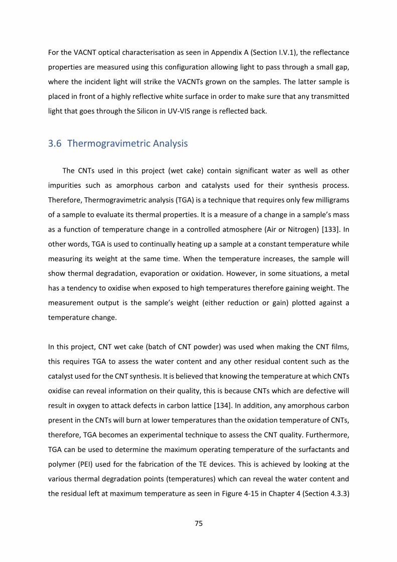
75
For the VACNT optical characterisation as seen in Appendix A (Section I.V.1), the reflectance
properties are measured using this configuration allowing light to pass through a small gap,
where the incident light will strike the VACNTs grown on the samples. The latter sample is
placed in front of a highly reflective white surface in order to make sure that any transmitted
light that goes through the Silicon in UV-VIS range is reflected back.
3.6 Thermogravimetric Analysis
The CNTs used in this project (wet cake) contain significant water as well as other
impurities such as amorphous carbon and catalysts used for their synthesis process.
Therefore, Thermogravimetric analysis (TGA) is a technique that requires only few milligrams
of a sample to evaluate its thermal properties. It is a measure of a change in a sample’s mass
as a function of temperature change in a controlled atmosphere (Air or Nitrogen) [133]. In
other words, TGA is used to continually heating up a sample at a constant temperature while
measuring its weight at the same time. When the temperature increases, the sample will
show thermal degradation, evaporation or oxidation. However, in some situations, a metal
has a tendency to oxidise when exposed to high temperatures therefore gaining weight. The
measurement output is the sample’s weight (either reduction or gain) plotted against a
temperature change.
In this project, CNT wet cake (batch of CNT powder) was used when making the CNT films,
this requires TGA to assess the water content and any other residual content such as the
catalyst used for the CNT synthesis. It is believed that knowing the temperature at which CNTs
oxidise can reveal information on their quality, this is because CNTs which are defective will
result in oxygen to attack defects in carbon lattice [134]. In addition, any amorphous carbon
present in the CNTs will burn at lower temperatures than the oxidation temperature of CNTs,
therefore, TGA becomes an experimental technique to assess the CNT quality. Furthermore,
TGA can be used to determine the maximum operating temperature of the surfactants and
polymer (PEI) used for the fabrication of the TE devices. This is achieved by looking at the
various thermal degradation points (temperatures) which can reveal the water content and
the residual left at maximum temperature as seen in Figure 4-15 in Chapter 4 (Section 4.3.3)
76
The TGA apparatus used to identify the amount of CNTs was TA Q500 TGA at the materials
lab, the measurements were performed in the air.
3.7 Summary
In this chapter, various characterisation techniques have been explored which are
important for this project in order to assess the different electrical structural properties of
the CNT films. Each analytical method has been introduced, highlighting their strengths of
proper implementation. For the electrical conductivity measurements, two different methods
are used which is necessary to confirm the data acquired from both of them.
Furthermore, an improvement of the test setup for Seebck coefficient measurement is
explained showing the difference between the old setup and the new one. In addition, an
emphasize on the importance of measuring the Seebeck coefficient as a function of
separation which will contribute into choosing the ideal length for the CNT films, thus
maximising the output power generated form the TE devices.
For the characterisation of the CNTs morphology, SEM spectroscopy was used which is
beneficial in analysing the individual CNTs and estimating the CNT films thicknesses. As for
the structural analysis of the CNTs, Raman has been described in detail, where each peak is
identified.
Finally, TGA is explored whose main purpose is to assess the amount of CNT content found in
the samples provided by Thomas Swan. Additionally, it will also be used for estimating the
thermal degradation point of each surfactant and polymer (PEI).
77
CNT films fabrication and characterisation
This chapter outlines the experimental methods used in the fabrication process of the
SWCNT films. To determine the power factor, the electrical conductivity and Seebeck
coefficient data are analysed, as well as the Raman data. The three sub-Sections of this
chapter are: characterisation of the Thomas Swan CNTs (SEM and TEM images of the non-
dispersed CNTs, their Raman signal and TGA data followed by the fabrication of SWCNT films
and TE devices for each surfactant and the characterisation of the TE devices and their
modules (n-type and p-type).
Previous work conducted in the field of TE device fabrication was done by various research
groups [14][96]-[101]. For example, Nonoguchi et al [135] investigated 33 organic compounds
as dopants for CNTs and measured their Seebeck coefficients and fabricated a TE device using
the best dopant. Another project was done by Dr Simon King at the University of Surrey [141]
where 7 surfactants were assessed for their feasibility in obtaining highly aligned areas of
electrospun CNT film nano-fibre. In this PhD project, the research is based on the same 7
surfactants which are used in fabricating the TE devices.
4.1 Characterisation of Thomas Swan CNTs
CNTs were provided by Thomas Swan and Co. Ltd. Their “Elicarb s-DWCNT” wet cake
was synthesised using a fluidized-bed chemical vapour deposition (CVD) method [52]. Iron
catalyst are filled in microscopic porous ceramic magnesium particles. After the growth
process, the particles are removed using hydrochloric acid followed by a wash in deionized
water (DW). According to the specifications (Product number PRO920), the average CNT
diameter is 0.9 - 1.7 nm with nanotube purity (Defined in Section 3.4) > 70% (catalyst residue,
ash and graphitic nanoparticles as the non-pure components) and ~ 4 µm in length. However,
for a more detail analysis and a better understanding of the physical and chemical properties
of the CNT wet cake, SEM and TEM imaging were done and Raman characterisation was
performed, in addition to TGA analysis. This will then ensure the effective use of these CNTs
in the films fabrications by determining the content of CNTs and whether or not there are
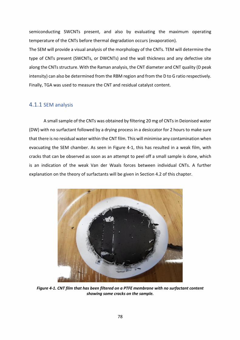
78
semiconducting SWCNTs present, and also by evaluating the maximum operating
temperature of the CNTs before thermal degradation occurs (evaporation).
The SEM will provide a visual analysis of the morphology of the CNTs. TEM will determine the
type of CNTs present (SWCNTs, or DWCNTs) and the wall thickness and any defective site
along the CNTs structure. With the Raman analysis, the CNT diameter and CNT quality (D peak
intensity) can also be determined from the RBM region and from the D to G ratio respectively.
Finally, TGA was used to measure the CNT and residual catalyst content.
4.1.1 SEM analysis
A small sample of the CNTs was obtained by filtering 20 mg of CNTs in Deionised water
(DW) with no surfactant followed by a drying process in a desiccator for 2 hours to make sure
that there is no residual water within the CNT film. This will minimise any contamination when
evacuating the SEM chamber. As seen in Figure 4-1, this has resulted in a weak film, with
cracks that can be observed as soon as an attempt to peel off a small sample is done, which
is an indication of the weak Van der Waals forces between individual CNTs. A further
explanation on the theory of surfactants will be given in Section 4.2 of this chapter.
Figure 4-1. CNT film that has been filtered on a PTFE membrane with no surfactant content showing some cracks on the sample.
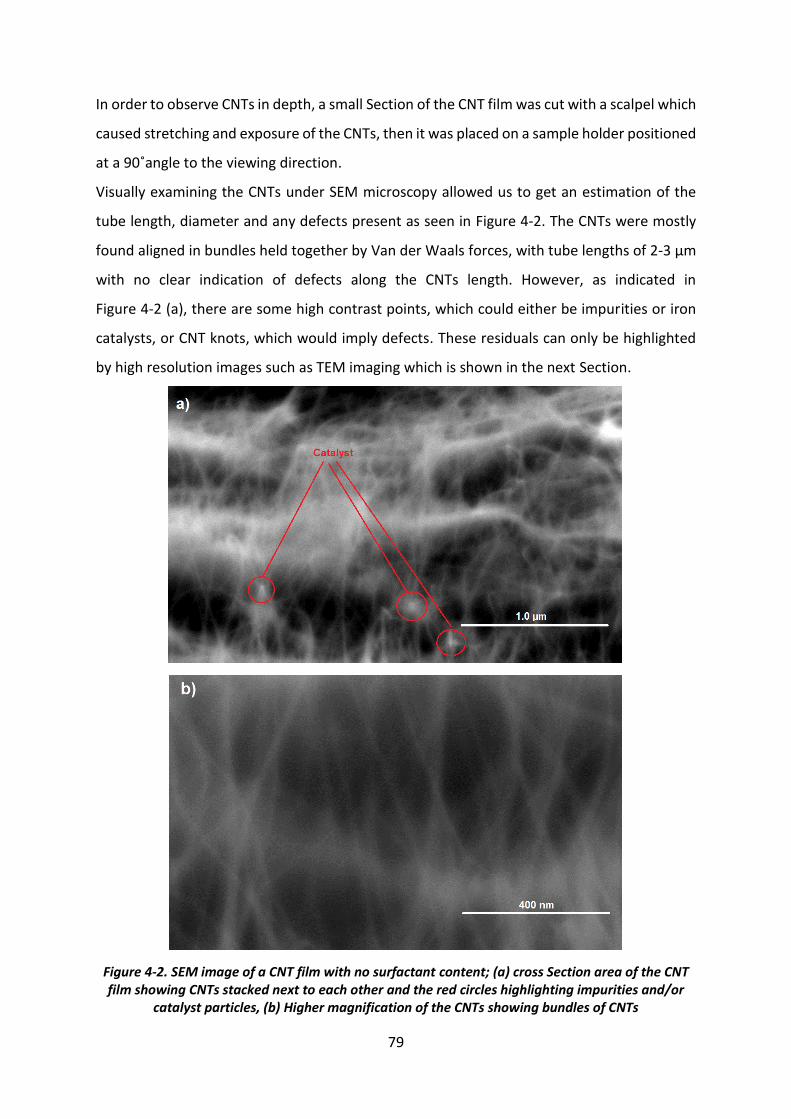
79
In order to observe CNTs in depth, a small Section of the CNT film was cut with a scalpel which
caused stretching and exposure of the CNTs, then it was placed on a sample holder positioned
at a 90˚angle to the viewing direction.
Visually examining the CNTs under SEM microscopy allowed us to get an estimation of the
tube length, diameter and any defects present as seen in Figure 4-2. The CNTs were mostly
found aligned in bundles held together by Van der Waals forces, with tube lengths of 2-3 µm
with no clear indication of defects along the CNTs length. However, as indicated in
Figure 4-2 (a), there are some high contrast points, which could either be impurities or iron
catalysts, or CNT knots, which would imply defects. These residuals can only be highlighted
by high resolution images such as TEM imaging which is shown in the next Section.
Figure 4-2. SEM image of a CNT film with no surfactant content; (a) cross Section area of the CNT film showing CNTs stacked next to each other and the red circles highlighting impurities and/or
catalyst particles, (b) Higher magnification of the CNTs showing bundles of CNTs
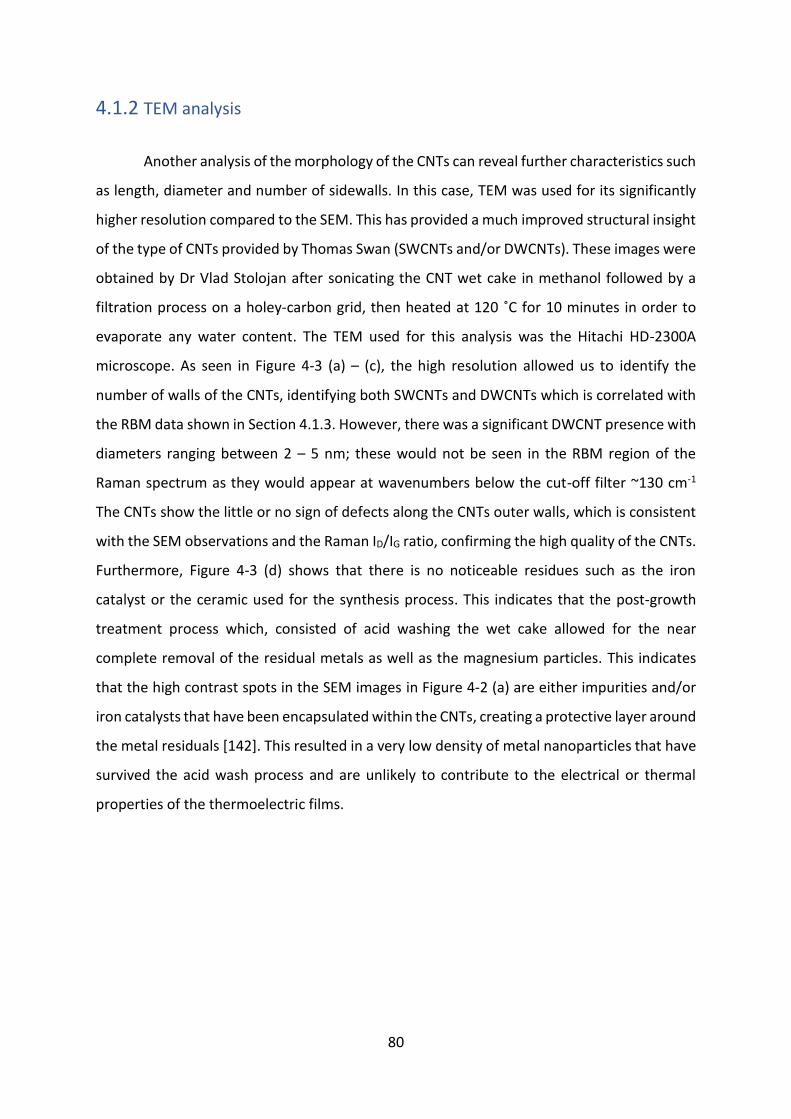
80
4.1.2 TEM analysis
Another analysis of the morphology of the CNTs can reveal further characteristics such
as length, diameter and number of sidewalls. In this case, TEM was used for its significantly
higher resolution compared to the SEM. This has provided a much improved structural insight
of the type of CNTs provided by Thomas Swan (SWCNTs and/or DWCNTs). These images were
obtained by Dr Vlad Stolojan after sonicating the CNT wet cake in methanol followed by a
filtration process on a holey-carbon grid, then heated at 120 ˚C for 10 minutes in order to
evaporate any water content. The TEM used for this analysis was the Hitachi HD-2300A
microscope. As seen in Figure 4-3 (a) – (c), the high resolution allowed us to identify the
number of walls of the CNTs, identifying both SWCNTs and DWCNTs which is correlated with
the RBM data shown in Section 4.1.3. However, there was a significant DWCNT presence with
diameters ranging between 2 – 5 nm; these would not be seen in the RBM region of the
Raman spectrum as they would appear at wavenumbers below the cut-off filter ~130 cm-1
The CNTs show the little or no sign of defects along the CNTs outer walls, which is consistent
with the SEM observations and the Raman ID/IG ratio, confirming the high quality of the CNTs.
Furthermore, Figure 4-3 (d) shows that there is no noticeable residues such as the iron
catalyst or the ceramic used for the synthesis process. This indicates that the post-growth
treatment process which, consisted of acid washing the wet cake allowed for the near
complete removal of the residual metals as well as the magnesium particles. This indicates
that the high contrast spots in the SEM images in Figure 4-2 (a) are either impurities and/or
iron catalysts that have been encapsulated within the CNTs, creating a protective layer around
the metal residuals [142]. This resulted in a very low density of metal nanoparticles that have
survived the acid wash process and are unlikely to contribute to the electrical or thermal
properties of the thermoelectric films.
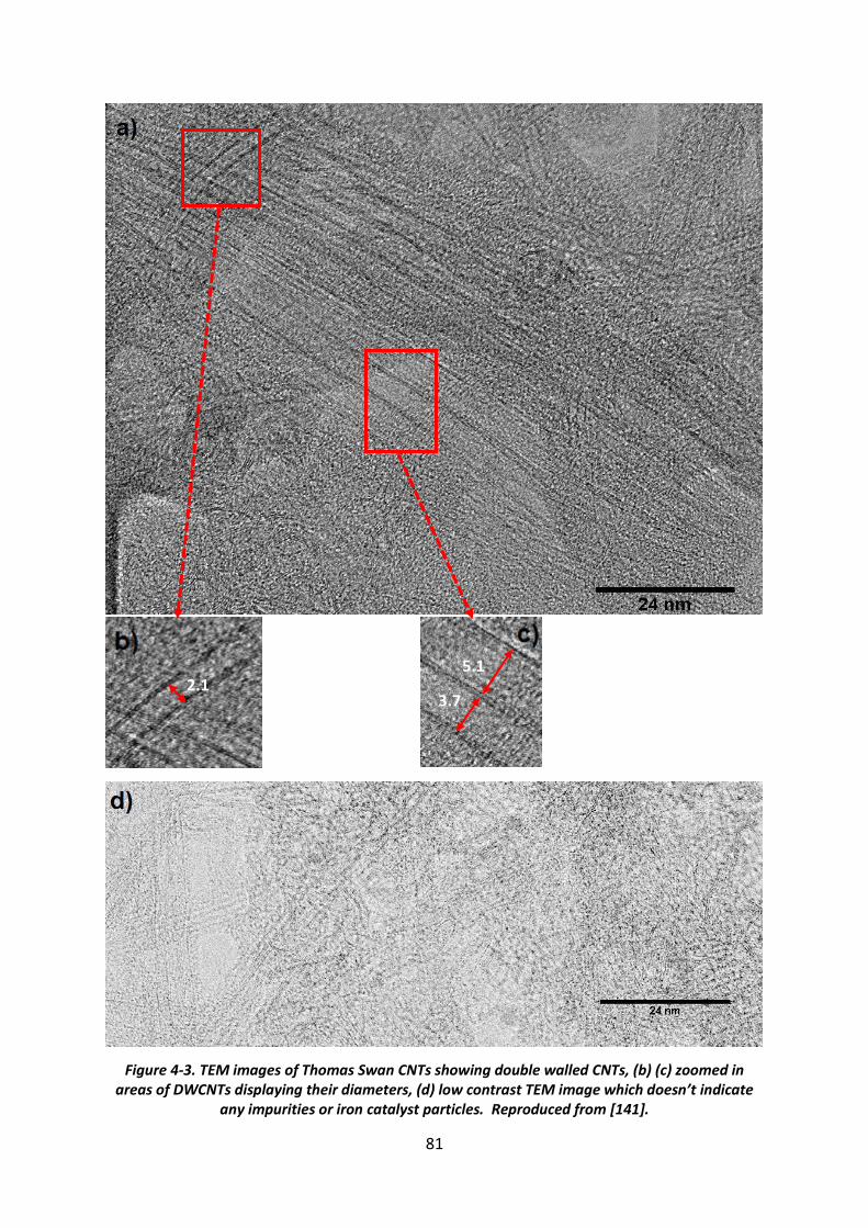
81
Figure 4-3. TEM images of Thomas Swan CNTs showing double walled CNTs, (b) (c) zoomed in areas of DWCNTs displaying their diameters, (d) low contrast TEM image which doesn’t indicate
any impurities or iron catalyst particles. Reproduced from [141].
5.1
3.7 2.1
82
4.1.3 Raman analysis
Raman Spectroscopy measurement was conducted on the CNT film described
previously in Section 4.1.1. Three Raman spectra were obtained using the red laser
(Elaser = 1.58 eV, 782 nm) from different spots of the CNT film and the average signal of the
three was taken. The resulting spectrum is shown in Figure 4-4.
From an initial analysis of the spectrum, it can be concluded that because of the low
background and the tall sharp peaks, this is really high purity CNTs [143]. If a sample has high
amorphous carbon content, the signal would be very noisy with a high D peak which would
require us to remove the background to better asses the Raman signal, however, in this case,
it wasn’t deemed necessary. Furthermore, the background is typically fluorescence which is
usually seen from amorphous carbon.
Figure 4-4. Raman spectrum of CNT film acquired from red laser 782 nm shows a typical Thomas Swan CNT sample with a D-G ratio of 0.15 displaying the regions of interest and key peaks.
0 500 1000 1500 2000 2500 3000
0.0
0.2
0.4
0.6
0.8
1.0 Pristine CNTs
2DiTOLA
M
G
Inte
nsity (
a.u
.)
Raman shift (cm-1)
RBM
D
Shoulder: G-
83
The first region of interest in the spectrum as shown in Figure 4-5 (a) displays the RBM region
or the Radial Breathing Mode (120 to 350 cm-1) which gives an indication of the different CNT
diameters depending of their Raman shift. There are four distinct broad peaks in this region
either SWCNTs or DWCNTs, therefore by applying Equation 3-5 from Chapter 3 (Section 3.4),
the diameter of the CNTs was calculated to be 1.61 nm, 1.2 nm, 1.05 nm and 0.93 nm. For
DWCNTs, it is known that the difference between the inner and outer tubes is 0.68 nm
according to Li et al [124], therefore, it can be seen that the CNTs with 0.93 nm and 1.61 nm
(difference is 0.68 nm) represent the inner and outer wall of a DWCNT.
In addition, the variations in the RBM intensity observed are dependent on the density of
states (DOS) available for the optical transitions for a particular type of CNT which includes
absorption and emission. For example, by using a tuneable laser, the joint DOS can be studied
which would allow the determination of the electronic structure of an isolated CNT at a
specific wavenumber (Raman shift). This could be achieved by plotting the resonance
intensity as a function of the value of the electronic transition energies (Eii) between the
valence bands and conduction bands [35] resulting in a resonance profile for a given (n,m)
nanotube.
To further asses the quality of the CNTs, we took into consideration the intensity of the D
peak and G peak. The ratio of ID/IG is 0.13 which is another strong indication that these CNTs
are of high quality due to the low number of defect sites within the CNT structure compared
to previously reported data [144].
When analysing the graphitic structure of the CNTs, the first and most intense peak is the G
peak. According to Dresselhaus [35], SWCNTs feature two peaks within the G peak, the G+
and the G- which are attributed to longitudinal optical (LO) and transverse optical (TO)
phonons respectively. However, for DWCNTs, we can observe four peaks, G+ and 3 G- modes
[124]. The splits displayed in the G peak can be seen in Figure 4-5 (b). This splitting is related
to the propagations of the phonons along the nanotube walls whether it is DWCNTs or
SWCNTs which will be described in Section 4.3.2.
The four peaks identified in the G peak indicate a mixture of both DWCNTs and SWCNTs,
therefore, by Looking into the G peak frequency shift which is normally located at
1581 cm-1 [143], in this particular case, the G peak is at 1587 cm-1; this confirms that the CNTs
are not dispersed (forming bundles) [145]. This is what to expect due to the experimental
procedure done for this Section, in other words, there was no surfactant added to the
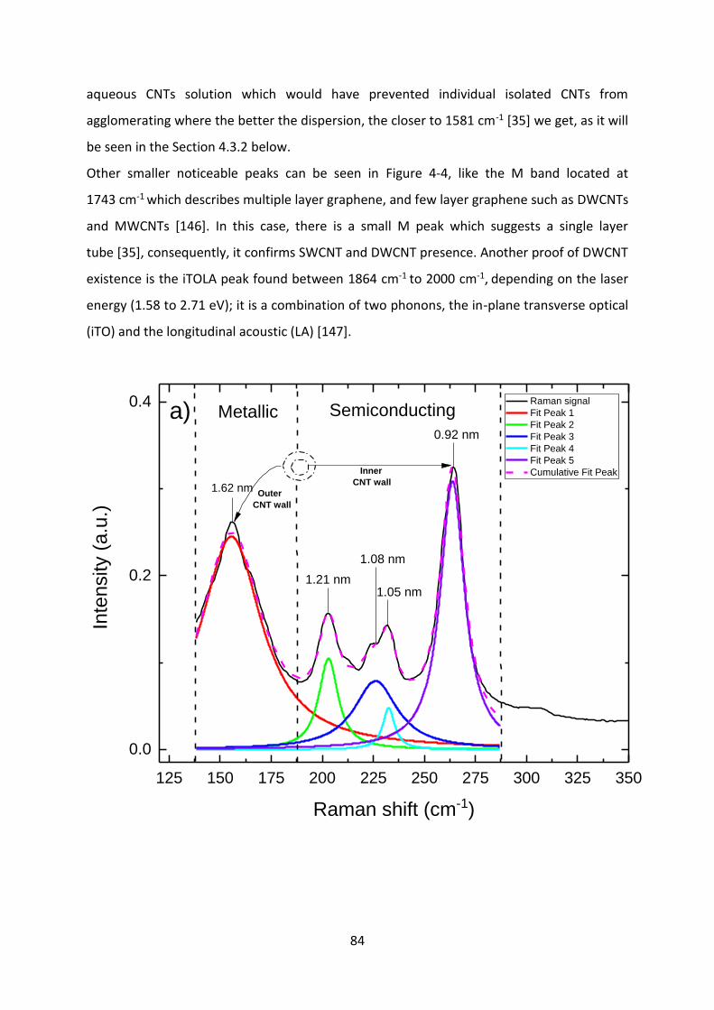
84
aqueous CNTs solution which would have prevented individual isolated CNTs from
agglomerating where the better the dispersion, the closer to 1581 cm-1 [35] we get, as it will
be seen in the Section 4.3.2 below.
Other smaller noticeable peaks can be seen in Figure 4-4, like the M band located at
1743 cm-1 which describes multiple layer graphene, and few layer graphene such as DWCNTs
and MWCNTs [146]. In this case, there is a small M peak which suggests a single layer
tube [35], consequently, it confirms SWCNT and DWCNT presence. Another proof of DWCNT
existence is the iTOLA peak found between 1864 cm-1 to 2000 cm-1, depending on the laser
energy (1.58 to 2.71 eV); it is a combination of two phonons, the in-plane transverse optical
(iTO) and the longitudinal acoustic (LA) [147].
125 150 175 200 225 250 275 300 325 350
0.0
0.2
0.4
Outer
CNT wall
a) Metallic Semiconducting
0.92 nm
1.05 nm
1.08 nm
1.21 nm
Inte
nsity (
a.u
.)
Raman shift (cm-1)
Raman signal
Fit Peak 1
Fit Peak 2
Fit Peak 3
Fit Peak 4
Fit Peak 5
Cumulative Fit Peak
1.62 nm
Inner
CNT wall
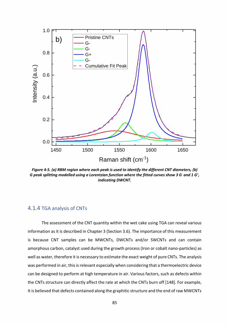
85
Figure 4-5. (a) RBM region where each peak is used to identify the different CNT diameters, (b) G peak splitting modelled using a Lorentzian function where the fitted curves show 3 G- and 1 G+,
indicating DWCNT.
4.1.4 TGA analysis of CNTs
The assessment of the CNT quantity within the wet cake using TGA can reveal various
information as it is described in Chapter 3 (Section 3.6). The importance of this measurement
is because CNT samples can be MWCNTs, DWCNTs and/or SWCNTs and can contain
amorphous carbon, catalyst used during the growth process (Iron or cobalt nano-particles) as
well as water, therefore it is necessary to estimate the exact weight of pure CNTs. The analysis
was performed in air, this is relevant especially when considering that a thermoelectric device
can be designed to perform at high temperature in air. Various factors, such as defects within
the CNTs structure can directly affect the rate at which the CNTs burn off [148]. For example,
It is believed that defects contained along the graphitic structure and the end of raw MWCNTs
1450 1500 1550 1600 1650
0.0
0.2
0.4
0.6
0.8
1.0
b)In
tensity (
a.u
.)
Raman shift (cm-1)
Pristine CNTs
G-
G-
G+
G-
Cumulative Fit PeakModel Lorentz
Equation y = y0 + (2*A/pi)*(w/(4*(x-xc)^2 + w^2))
Plot Peak1(Raman signal) Peak2(Raman signal) Peak3(Raman signal) Peak4(Raman signal)
y0* 0 ± 0 0 ± 0 0 ± 0 0 ± 0
xc 1542.73377 ± 2.83551 1559.61944 ± 0.26082 1587.648 ± 0.10767 1601.25921 ± 1.03628
w 93.35907 ± 2.6385 29.9708 ± 1.76692 22.89176 ± 0.36055 22.27137 ± 2.45613
A 14.76177 ± 1.23476 8.11399 ± 0.94922 31.42379 ± 0.94396 3.03878 ± 0.8279
y0 0 ± 0 0 ± 0 0 ± 0 0 ± 0
Reduced Chi-Sqr 3.54175E-5
R-Square(COD) 0.99946
Adj. R-Square 0.99944
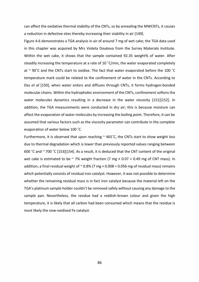
86
can affect the oxidative thermal stability of the CNTs, so by annealing the MWCNTs, it causes
a reduction in defective sites thereby increasing their stability in air [149].
Figure 4-6 demonstrates a TGA analysis in air of around 7 mg of wet cake; the TGA data used
in this chapter was acquired by Mrs Violeta Doukova from the Surrey Materials Institute.
Within the wet cake, it shows that the sample contained 92.35 weight% of water. After
steadily increasing the temperature at a rate of 10 ˚C/min, the water evaporated completely
at ~ 90˚C and the CNTs start to oxidise. The fact that water evaporated before the 100 ˚C
temperature mark could be related to the confinement of water in the CNTs. According to
Das et al [150], when water enters and diffuses through CNTs, it forms hydrogen-bonded
molecular chains. Within the hydrophobic environment of the CNTs, confinement softens the
water molecules dynamics resulting in a decrease in the water viscosity [151][152]. In
addition, the TGA measurements were conducted in dry air; this is because moisture can
affect the evaporation of water molecules by increasing the boiling point. Therefore, it can be
assumed that various factors such as the viscosity parameter can contribute in the complete
evaporation of water below 100 ˚C.
Furthermore, it is observed that upon reaching ~ 465˚C, the CNTs start to show weight loss
due to thermal degradation which is lower than previously reported values ranging between
600 ˚C and ~ 700 ˚C [153][154]. As a result, it is deduced that the CNT content of the original
wet cake is estimated to be ~ 7% weight fraction (7 mg × 0.07 = 0.49 mg of CNT mass). In
addition, a final residual weight of ~ 0.8% (7 mg × 0.008 = 0.056 mg of residual mass) remains
which potentially consists of residual iron catalyst. However, it was not possible to determine
whether the remaining residual mass is in fact iron catalyst because the material left on the
TGA’s platinum sample holder couldn’t be removed safely without causing any damage to the
sample pan. Nevertheless, the residue had a reddish-brown colour and given the high
temperature, it is likely that all carbon had been consumed which means that the residue is
most likely the now-oxidised Fe catalyst.
87
Figure 4-6. TGA graph obtained from ~ 7 mg of CNTs from a batch produced by Thomas Swan and Co. Ltd, measured in air with 92.35% water content and only ~ 7% CNT weight fraction and ~ 0.8%
residual mass.
4.2 p-type and n-type CNT films fabrication
In this Section, a detailed investigation was done on different CNT samples mixed with
seven surfactants (Anionic, non-ionic and cationic), as shown in Table 4-1 and Figure 4-7.
The choice of these surfactants is based on previous work conducted at the ATI [141]; the
work consisted of investigating CNTs dispersion using the surfactants listed in Table 4-1 and
others non-listed ones (Brij 52, Triton X-100), which vary depending on their hydrophilic end
polarity. Prior to that work, the literature had shown that there has been extensive work done
on SDS in dispersing CNTs in aqueous solution, resulting in successful dispersions making it a
reliable surfactant. This has made it broadly available at a research and industrial levels due
to its known performance in achieving greater loadings for electrospinning purposes
[155][156]. Regardless, there was no data available in quantifying surfactant performances in
0 100 200 300 400 500 600 700
0
20
40
60
80
100
6.825% CNT mass
Temperature (°C)
Weig
ht (%
)
92.35% water
72 C
Highest rate of change
588 C
0.0
0.5
1.0
1.5
2.0
2.5
0.825%
residual mass
CNT wet cake
Deri. W
eig
ht (%
/min
)
Measured in Air
90 C
Highest evaporation point
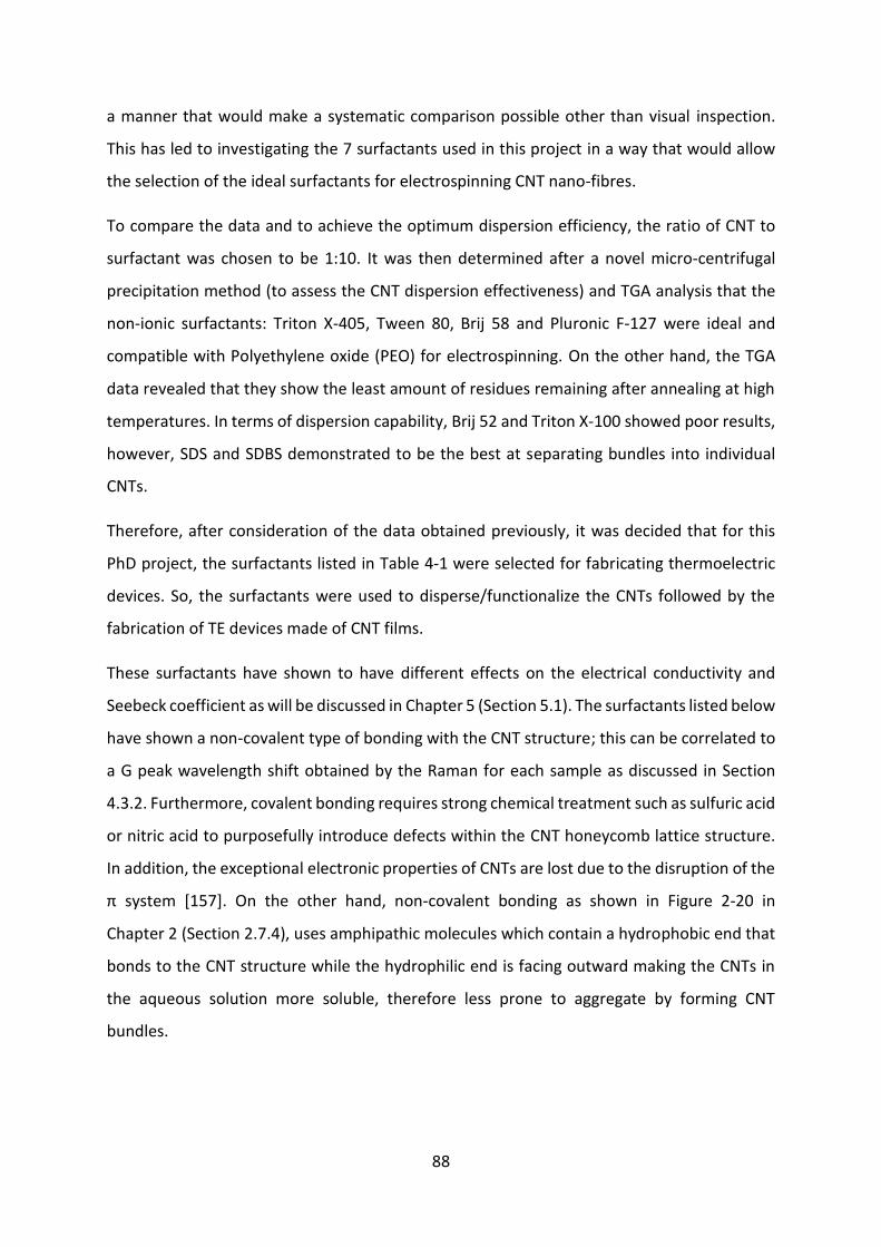
88
a manner that would make a systematic comparison possible other than visual inspection.
This has led to investigating the 7 surfactants used in this project in a way that would allow
the selection of the ideal surfactants for electrospinning CNT nano-fibres.
To compare the data and to achieve the optimum dispersion efficiency, the ratio of CNT to
surfactant was chosen to be 1:10. It was then determined after a novel micro-centrifugal
precipitation method (to assess the CNT dispersion effectiveness) and TGA analysis that the
non-ionic surfactants: Triton X-405, Tween 80, Brij 58 and Pluronic F-127 were ideal and
compatible with Polyethylene oxide (PEO) for electrospinning. On the other hand, the TGA
data revealed that they show the least amount of residues remaining after annealing at high
temperatures. In terms of dispersion capability, Brij 52 and Triton X-100 showed poor results,
however, SDS and SDBS demonstrated to be the best at separating bundles into individual
CNTs.
Therefore, after consideration of the data obtained previously, it was decided that for this
PhD project, the surfactants listed in Table 4-1 were selected for fabricating thermoelectric
devices. So, the surfactants were used to disperse/functionalize the CNTs followed by the
fabrication of TE devices made of CNT films.
These surfactants have shown to have different effects on the electrical conductivity and
Seebeck coefficient as will be discussed in Chapter 5 (Section 5.1). The surfactants listed below
have shown a non-covalent type of bonding with the CNT structure; this can be correlated to
a G peak wavelength shift obtained by the Raman for each sample as discussed in Section
4.3.2. Furthermore, covalent bonding requires strong chemical treatment such as sulfuric acid
or nitric acid to purposefully introduce defects within the CNT honeycomb lattice structure.
In addition, the exceptional electronic properties of CNTs are lost due to the disruption of the
π system [157]. On the other hand, non-covalent bonding as shown in Figure 2-20 in
Chapter 2 (Section 2.7.4), uses amphipathic molecules which contain a hydrophobic end that
bonds to the CNT structure while the hydrophilic end is facing outward making the CNTs in
the aqueous solution more soluble, therefore less prone to aggregate by forming CNT
bundles.
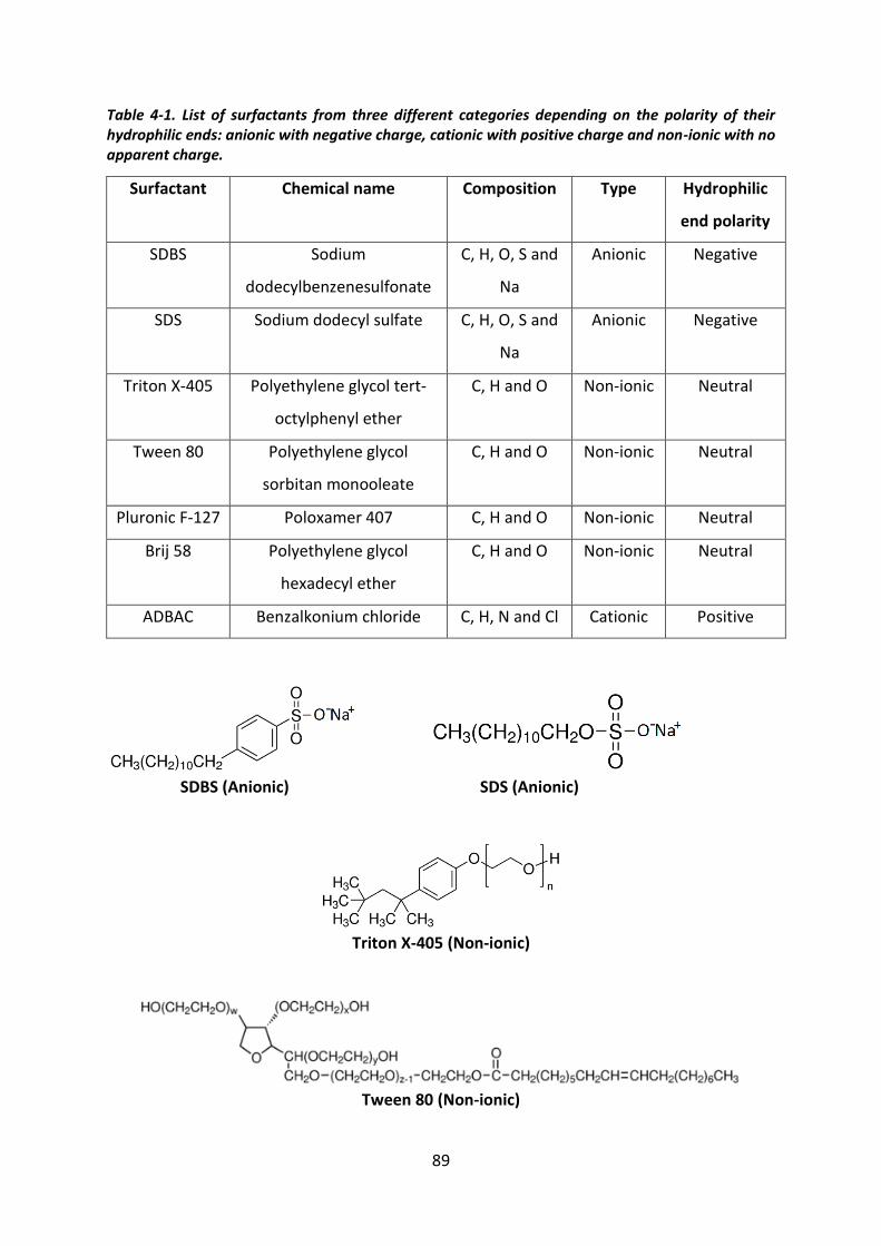
89
Table 4-1. List of surfactants from three different categories depending on the polarity of their hydrophilic ends: anionic with negative charge, cationic with positive charge and non-ionic with no apparent charge.
Surfactant Chemical name Composition Type Hydrophilic
end polarity
SDBS Sodium
dodecylbenzenesulfonate
C, H, O, S and
Na
Anionic Negative
SDS Sodium dodecyl sulfate C, H, O, S and
Na
Anionic Negative
Triton X-405 Polyethylene glycol tert-
octylphenyl ether
C, H and O Non-ionic Neutral
Tween 80 Polyethylene glycol
sorbitan monooleate
C, H and O Non-ionic Neutral
Pluronic F-127 Poloxamer 407 C, H and O Non-ionic Neutral
Brij 58 Polyethylene glycol
hexadecyl ether
C, H and O Non-ionic Neutral
ADBAC Benzalkonium chloride C, H, N and Cl Cationic Positive
SDBS (Anionic) SDS (Anionic)
Triton X-405 (Non-ionic)
Tween 80 (Non-ionic)
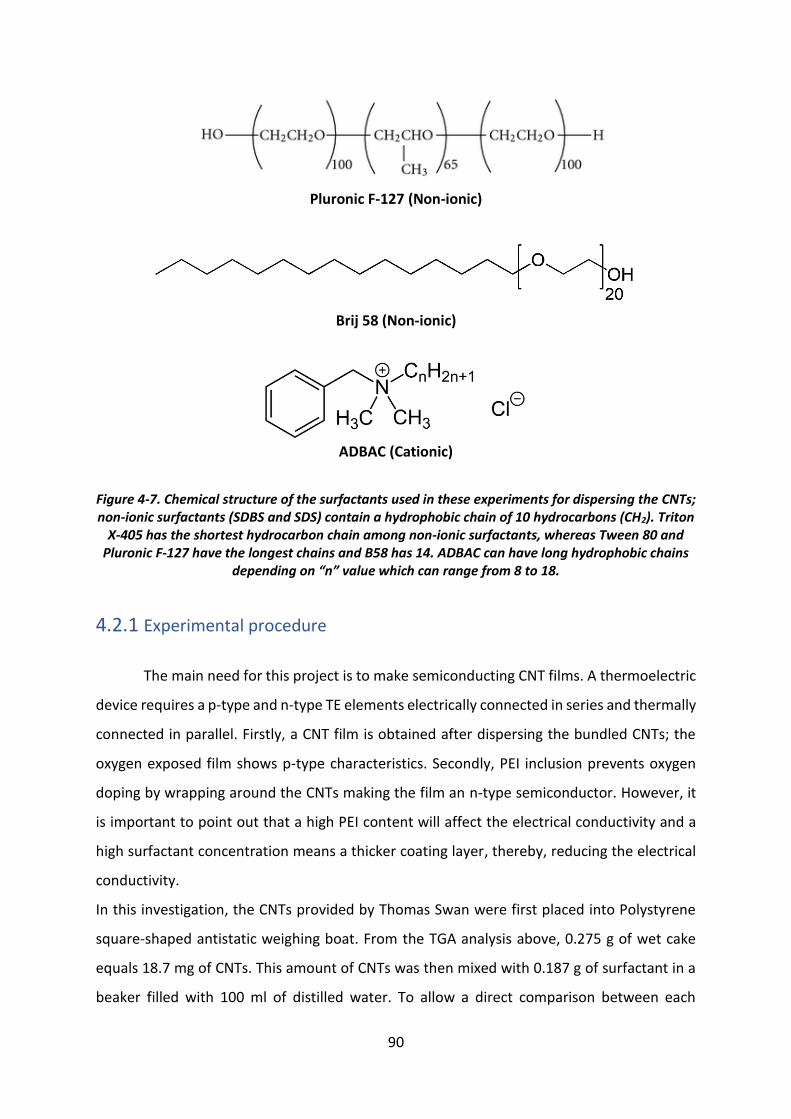
90
Pluronic F-127 (Non-ionic)
Brij 58 (Non-ionic)
ADBAC (Cationic)
Figure 4-7. Chemical structure of the surfactants used in these experiments for dispersing the CNTs; non-ionic surfactants (SDBS and SDS) contain a hydrophobic chain of 10 hydrocarbons (CH2). Triton
X-405 has the shortest hydrocarbon chain among non-ionic surfactants, whereas Tween 80 and Pluronic F-127 have the longest chains and B58 has 14. ADBAC can have long hydrophobic chains
depending on “n” value which can range from 8 to 18.
4.2.1 Experimental procedure
The main need for this project is to make semiconducting CNT films. A thermoelectric
device requires a p-type and n-type TE elements electrically connected in series and thermally
connected in parallel. Firstly, a CNT film is obtained after dispersing the bundled CNTs; the
oxygen exposed film shows p-type characteristics. Secondly, PEI inclusion prevents oxygen
doping by wrapping around the CNTs making the film an n-type semiconductor. However, it
is important to point out that a high PEI content will affect the electrical conductivity and a
high surfactant concentration means a thicker coating layer, thereby, reducing the electrical
conductivity.
In this investigation, the CNTs provided by Thomas Swan were first placed into Polystyrene
square-shaped antistatic weighing boat. From the TGA analysis above, 0.275 g of wet cake
equals 18.7 mg of CNTs. This amount of CNTs was then mixed with 0.187 g of surfactant in a
beaker filled with 100 ml of distilled water. To allow a direct comparison between each
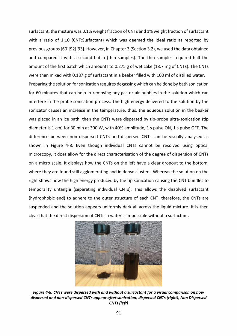
91
surfactant, the mixture was 0.1% weight fraction of CNTs and 1% weight fraction of surfactant
with a ratio of 1:10 (CNT:Surfactant) which was deemed the ideal ratio as reported by
previous groups [60][92][93]. However, in Chapter 3 (Section 3.2), we used the data obtained
and compared it with a second batch (thin samples). The thin samples required half the
amount of the first batch which amounts to 0.275 g of wet cake (18.7 mg of CNTs). The CNTs
were then mixed with 0.187 g of surfactant in a beaker filled with 100 ml of distilled water.
Preparing the solution for sonication requires degassing which can be done by bath sonication
for 60 minutes that can help in removing any gas or air bubbles in the solution which can
interfere in the probe sonication process. The high energy delivered to the solution by the
sonicator causes an increase in the temperature, thus, the aqueous solution in the beaker
was placed in an ice bath, then the CNTs were dispersed by tip-probe ultra-sonication (tip
diameter is 1 cm) for 30 min at 300 W, with 40% amplitude, 1 s pulse ON, 1 s pulse OFF. The
difference between non dispersed CNTs and dispersed CNTs can be visually analysed as
shown in Figure 4-8. Even though individual CNTs cannot be resolved using optical
microscopy, it does allow for the direct characterisation of the degree of dispersion of CNTs
on a micro scale. It displays how the CNTs on the left have a clear dropout to the bottom,
where they are found still agglomerating and in dense clusters. Whereas the solution on the
right shows how the high energy produced by the tip sonication causing the CNT bundles to
temporality untangle (separating individual CNTs). This allows the dissolved surfactant
(hydrophobic end) to adhere to the outer structure of each CNT, therefore, the CNTs are
suspended and the solution appears uniformly dark all across the liquid mixture. It is then
clear that the direct dispersion of CNTs in water is impossible without a surfactant.
Figure 4-8. CNTs were dispersed with and without a surfactant for a visual comparison on how dispersed and non-dispersed CNTs appear after sonication; dispersed CNTs (right), Non Dispersed
CNTs (left)
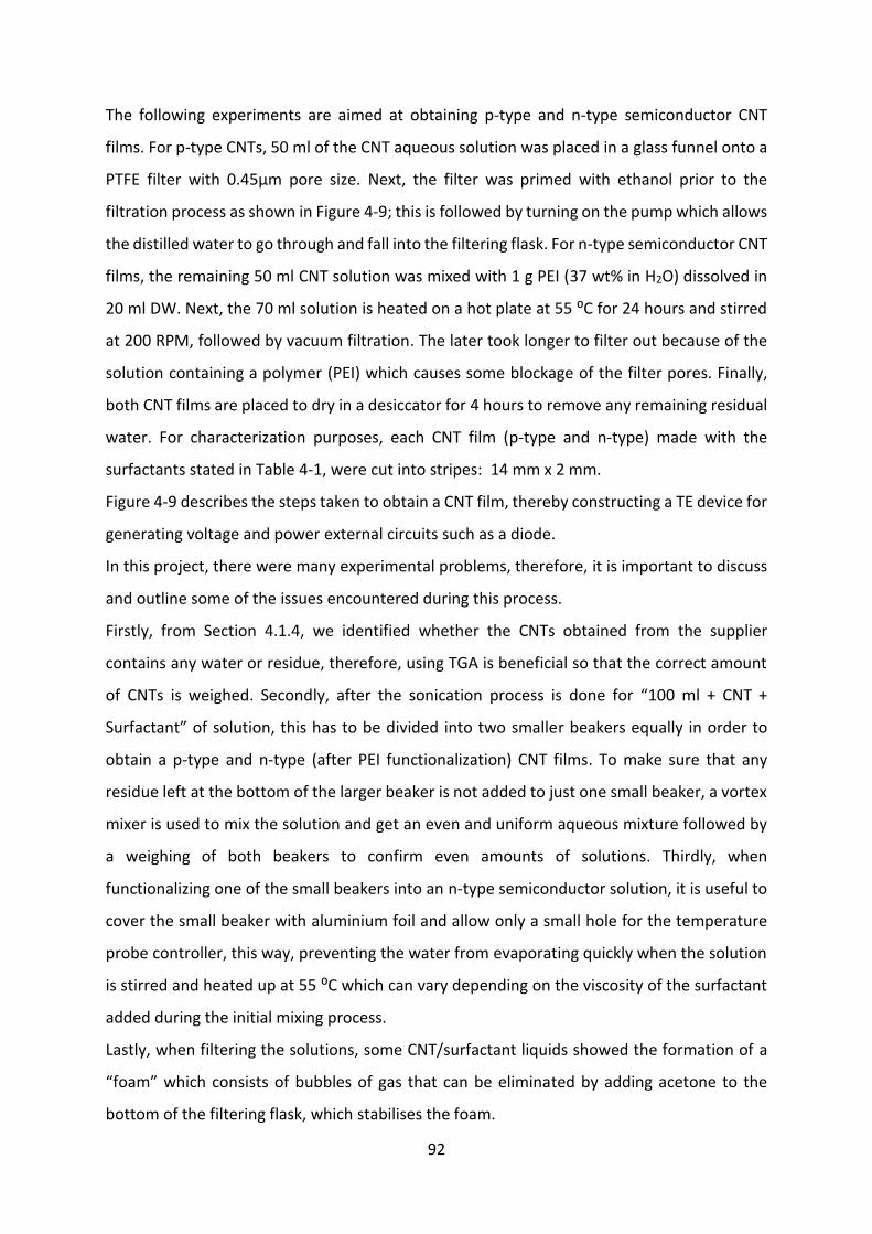
92
The following experiments are aimed at obtaining p-type and n-type semiconductor CNT
films. For p-type CNTs, 50 ml of the CNT aqueous solution was placed in a glass funnel onto a
PTFE filter with 0.45µm pore size. Next, the filter was primed with ethanol prior to the
filtration process as shown in Figure 4-9; this is followed by turning on the pump which allows
the distilled water to go through and fall into the filtering flask. For n-type semiconductor CNT
films, the remaining 50 ml CNT solution was mixed with 1 g PEI (37 wt% in H2O) dissolved in
20 ml DW. Next, the 70 ml solution is heated on a hot plate at 55 ⁰C for 24 hours and stirred
at 200 RPM, followed by vacuum filtration. The later took longer to filter out because of the
solution containing a polymer (PEI) which causes some blockage of the filter pores. Finally,
both CNT films are placed to dry in a desiccator for 4 hours to remove any remaining residual
water. For characterization purposes, each CNT film (p-type and n-type) made with the
surfactants stated in Table 4-1, were cut into stripes: 14 mm x 2 mm.
Figure 4-9 describes the steps taken to obtain a CNT film, thereby constructing a TE device for
generating voltage and power external circuits such as a diode.
In this project, there were many experimental problems, therefore, it is important to discuss
and outline some of the issues encountered during this process.
Firstly, from Section 4.1.4, we identified whether the CNTs obtained from the supplier
contains any water or residue, therefore, using TGA is beneficial so that the correct amount
of CNTs is weighed. Secondly, after the sonication process is done for “100 ml + CNT +
Surfactant” of solution, this has to be divided into two smaller beakers equally in order to
obtain a p-type and n-type (after PEI functionalization) CNT films. To make sure that any
residue left at the bottom of the larger beaker is not added to just one small beaker, a vortex
mixer is used to mix the solution and get an even and uniform aqueous mixture followed by
a weighing of both beakers to confirm even amounts of solutions. Thirdly, when
functionalizing one of the small beakers into an n-type semiconductor solution, it is useful to
cover the small beaker with aluminium foil and allow only a small hole for the temperature
probe controller, this way, preventing the water from evaporating quickly when the solution
is stirred and heated up at 55 ⁰C which can vary depending on the viscosity of the surfactant
added during the initial mixing process.
Lastly, when filtering the solutions, some CNT/surfactant liquids showed the formation of a
“foam” which consists of bubbles of gas that can be eliminated by adding acetone to the
bottom of the filtering flask, which stabilises the foam.
93
Figure 4-9. Experimental procedures for obtaining a CNT film; (a) probe sonicator used to disperse
CNTs while allowing surfactant particles to adhere to the CNT outer structure, (b) Hot plate to heat up the beaker and a temperature probe immersed into the solution to accurately obtain the
desired 55 ⁰C, (c) a vacuum filter system where the solution is poured into the Buchner funnel to obtain a CNT film, (d) a circular shape CNT film that can be cut into specific dimensions.
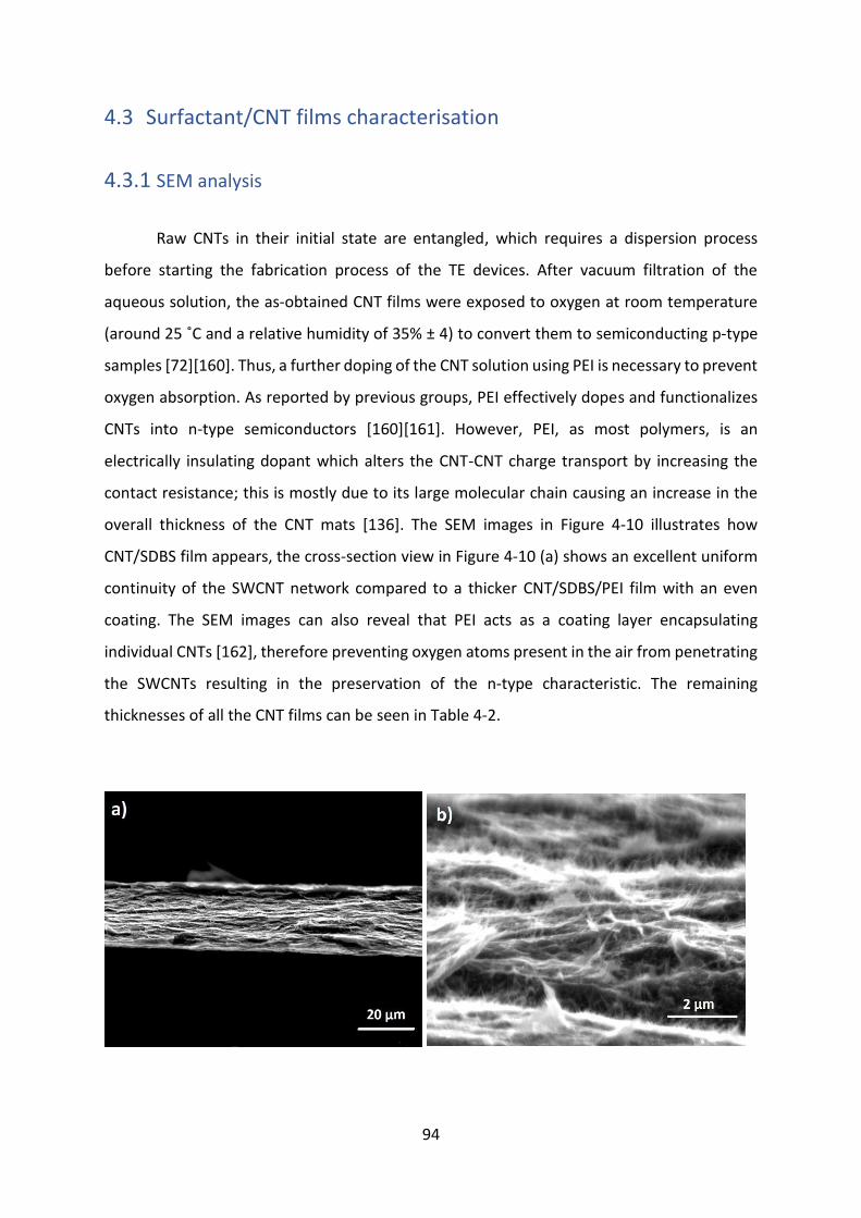
94
4.3 Surfactant/CNT films characterisation
4.3.1 SEM analysis
Raw CNTs in their initial state are entangled, which requires a dispersion process
before starting the fabrication process of the TE devices. After vacuum filtration of the
aqueous solution, the as-obtained CNT films were exposed to oxygen at room temperature
(around 25 ˚C and a relative humidity of 35% ± 4) to convert them to semiconducting p-type
samples [72][160]. Thus, a further doping of the CNT solution using PEI is necessary to prevent
oxygen absorption. As reported by previous groups, PEI effectively dopes and functionalizes
CNTs into n-type semiconductors [160][161]. However, PEI, as most polymers, is an
electrically insulating dopant which alters the CNT-CNT charge transport by increasing the
contact resistance; this is mostly due to its large molecular chain causing an increase in the
overall thickness of the CNT mats [136]. The SEM images in Figure 4-10 illustrates how
CNT/SDBS film appears, the cross-section view in Figure 4-10 (a) shows an excellent uniform
continuity of the SWCNT network compared to a thicker CNT/SDBS/PEI film with an even
coating. The SEM images can also reveal that PEI acts as a coating layer encapsulating
individual CNTs [162], therefore preventing oxygen atoms present in the air from penetrating
the SWCNTs resulting in the preservation of the n-type characteristic. The remaining
thicknesses of all the CNT films can be seen in Table 4-2.
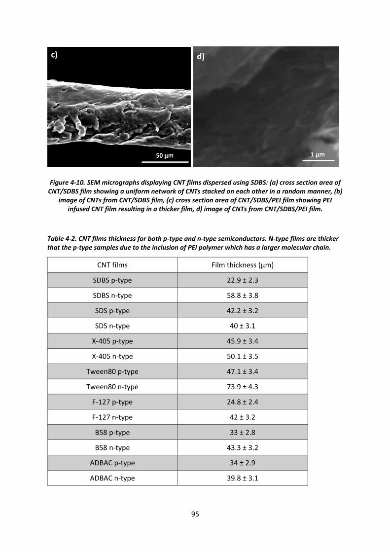
95
Figure 4-10. SEM micrographs displaying CNT films dispersed using SDBS: (a) cross section area of CNT/SDBS film showing a uniform network of CNTs stacked on each other in a random manner, (b)
image of CNTs from CNT/SDBS film, (c) cross section area of CNT/SDBS/PEI film showing PEI infused CNT film resulting in a thicker film, d) image of CNTs from CNT/SDBS/PEI film.
Table 4-2. CNT films thickness for both p-type and n-type semiconductors. N-type films are thicker that the p-type samples due to the inclusion of PEI polymer which has a larger molecular chain.
CNT films Film thickness (µm)
SDBS p-type 22.9 ± 2.3
SDBS n-type 58.8 ± 3.8
SDS p-type 42.2 ± 3.2
SDS n-type 40 ± 3.1
X-405 p-type 45.9 ± 3.4
X-405 n-type 50.1 ± 3.5
Tween80 p-type 47.1 ± 3.4
Tween80 n-type 73.9 ± 4.3
F-127 p-type 24.8 ± 2.4
F-127 n-type 42 ± 3.2
B58 p-type 33 ± 2.8
B58 n-type 43.3 ± 3.2
ADBAC p-type 34 ± 2.9
ADBAC n-type 39.8 ± 3.1
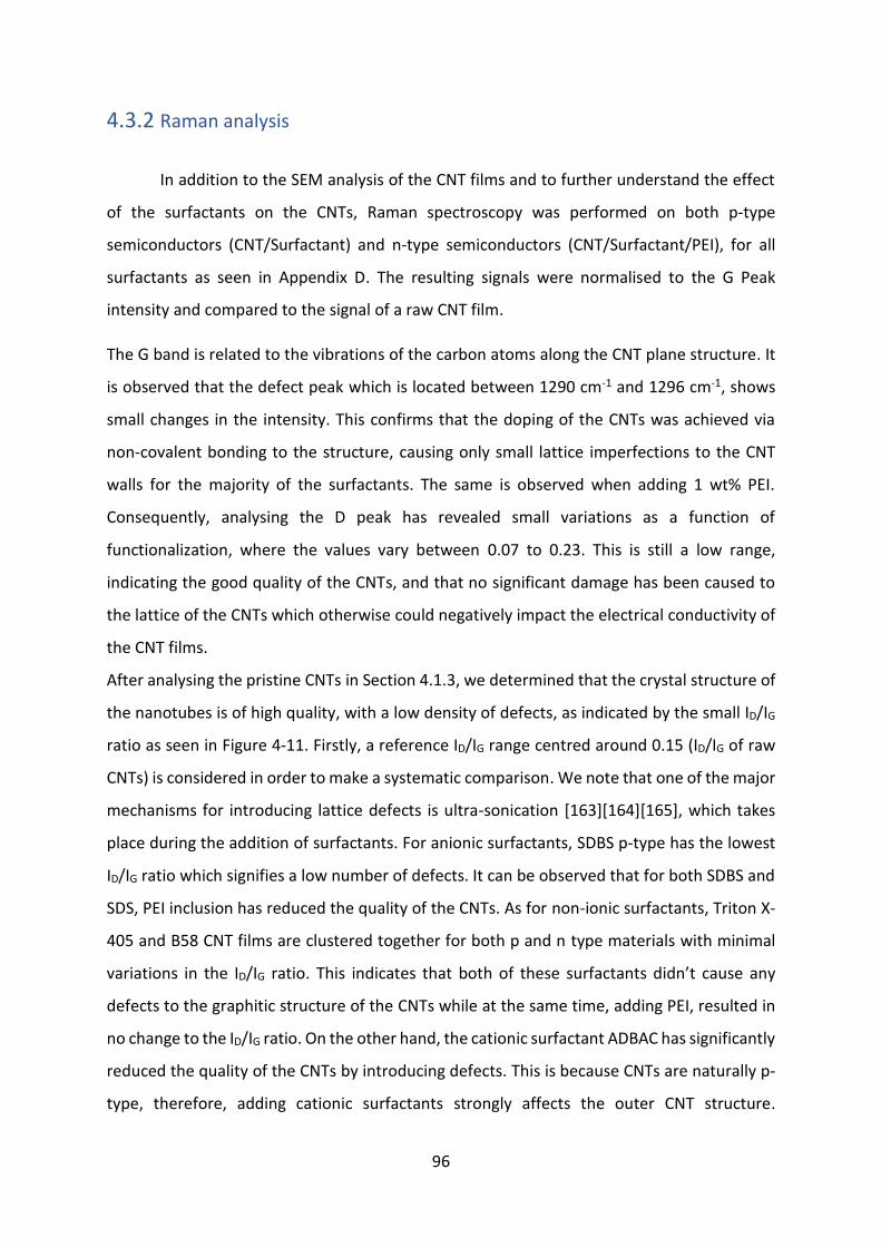
96
4.3.2 Raman analysis
In addition to the SEM analysis of the CNT films and to further understand the effect
of the surfactants on the CNTs, Raman spectroscopy was performed on both p-type
semiconductors (CNT/Surfactant) and n-type semiconductors (CNT/Surfactant/PEI), for all
surfactants as seen in Appendix D. The resulting signals were normalised to the G Peak
intensity and compared to the signal of a raw CNT film.
The G band is related to the vibrations of the carbon atoms along the CNT plane structure. It
is observed that the defect peak which is located between 1290 cm-1 and 1296 cm-1, shows
small changes in the intensity. This confirms that the doping of the CNTs was achieved via
non-covalent bonding to the structure, causing only small lattice imperfections to the CNT
walls for the majority of the surfactants. The same is observed when adding 1 wt% PEI.
Consequently, analysing the D peak has revealed small variations as a function of
functionalization, where the values vary between 0.07 to 0.23. This is still a low range,
indicating the good quality of the CNTs, and that no significant damage has been caused to
the lattice of the CNTs which otherwise could negatively impact the electrical conductivity of
the CNT films.
After analysing the pristine CNTs in Section 4.1.3, we determined that the crystal structure of
the nanotubes is of high quality, with a low density of defects, as indicated by the small ID/IG
ratio as seen in Figure 4-11. Firstly, a reference ID/IG range centred around 0.15 (ID/IG of raw
CNTs) is considered in order to make a systematic comparison. We note that one of the major
mechanisms for introducing lattice defects is ultra-sonication [163][164][165], which takes
place during the addition of surfactants. For anionic surfactants, SDBS p-type has the lowest
ID/IG ratio which signifies a low number of defects. It can be observed that for both SDBS and
SDS, PEI inclusion has reduced the quality of the CNTs. As for non-ionic surfactants, Triton X-
405 and B58 CNT films are clustered together for both p and n type materials with minimal
variations in the ID/IG ratio. This indicates that both of these surfactants didn’t cause any
defects to the graphitic structure of the CNTs while at the same time, adding PEI, resulted in
no change to the ID/IG ratio. On the other hand, the cationic surfactant ADBAC has significantly
reduced the quality of the CNTs by introducing defects. This is because CNTs are naturally p-
type, therefore, adding cationic surfactants strongly affects the outer CNT structure.
97
According to Matarredona et al [166], it is believed that depending on the pH of the
surrounding environment, CNTs can exhibit either a positive or a negative charge. Also, CNTs
interact with the hydrophobic end of the surfactant. Thus, if the CNT outer structure is
polarised, the Coulombic repulsion or attraction forces between the CNT wall and the charged
hydrophilic groups of the surfactant can occur which can significantly increase solubility.
Adding PEI to the mixture has significantly increased the quality of the CNTs which acted as a
binding chemical agent at the defect sites.
Figure 4-11. Graph displaying the ID/IG ratio of the CNT films (open symbols are for p-type CNTs and closed symbols are for n-type CNTs); the low values obtained are a strong indication of good
quality CNTs. SDBS p-type film shows the lowest ratio due to the low density of defects. ADBAC p-type film has the highest ratio, but when adding PEI, the ID/IG ratio drops significantly meaning
that PEI acted as a binding chemical agent.
Raw
CN
Ts
SD
BS
p-t
ype
SD
BS
n-T
ype
SD
S p
-type
SD
S n
-type
X405 p
-type
X405 n
-type
Tw
een80 p
-type
Tw
een80 n
-type
F127 p
-type
F127 n
-type
B58 p
-type
B58 n
-type
AD
BA
C p
-type
AD
BA
C n
-type
0.06
0.09
0.12
0.15
0.18
0.21
0.24
0.27
0.30
0 500 1000 1500 2000 2500 3000
0.0
0.2
0.4
0.6
0.8
1.0 Inset graph
Inte
nsit
y (
a.u
.)
Raman shift (cm-1)
Cationic
surfactants
Non-ionic
surfactants
I D/I
G r
atio
CNT films
Anionic
surfactants
Reference D/G range
98
After analysing the quality of the CNTs by looking at the ID/IG ratio, we now look at the degree
of dispersion of CNT bundles. This is achieved by assessing the effect of surfactants on the
frequency shift of the Raman G peak; this is because the hydrophobic end of the surfactant
bonds with the outer structure of the CNTs. As discussed in Chapter 2 (Section 2.5.4), CNTs in
their natural state after synthesis are closely packed together in bundles due to Van der Waal
forces [98]. A bundle of CNTs can have any number of entangled CNTs, agglomerating
together with an attraction energy estimated to be 500 eV/μm of tube-tube contact
[167][168]. In order to disperse CNTs in water, surfactant molecules are directed in a way that
allows their hydrophobic tails to face toward the CNTs while the hydrophilic ends are facing
towards water as shown in Figure 2-20 in Chapter 2 (Section 2.7.4).
As a result, the surfactant’s main role is to separate CNT bundles during the ultra-sonication
process in order to obtain CNT films after vacuum filtration, therefore, the reason for this
analysis is relating the dispersion to the G peak wavenumber. This will cause a red shift in the
G peak frequency as shown in Figure 4-12.
It is known that the G peak is associated with the longitudinal optical (LO) phonon mode in
which the vibrations occur along the nanotube axis [169]. Its wavenumber ωG+ is sensitive to
the addition of dopants during the charge transfer between carbon atoms and, in this case;
surfactants and PEI, where the blue shift is for acceptors (holes/p-type) and red shift is for
donors (electrons/n-type) [170].
Generally, it is thought that because the hexagonal units of hydrophobic chains match well
with the carbon unit cells, the hydrophobic tail groups tend to lie flat on the CNTs surface
[171]. Therefore, the hydrophobic tail length of a surfactant greatly affects the molecules
absorption and consequently the dispersion.
The data from Figure 4-12 gives a comparative Raman analysis of the CNT films dispersed
using the surfactants listed in Table 4-1 in Section 4.2, and the PEI doped CNTs. It is noticed
that the G peak frequency shift ranges from 1587 cm-1 to 1583 cm-1 for all the CNT/Surfactant
mixture. Furthermore, the degree of dispersion can have a direct impact on the homogeneity
and stability of the CNT film, therefore, a valid method of analysing the state of dispersion is
by visual inspection [172]. For example, the G peak frequency for the pristine CNT film is at
1587 cm-1; this has resulted in poor mechanical properties that can be observed on the CNT
film as shown in Figure 4-1 in Section 4.1.1 where cracks are visible. As a result, it can be
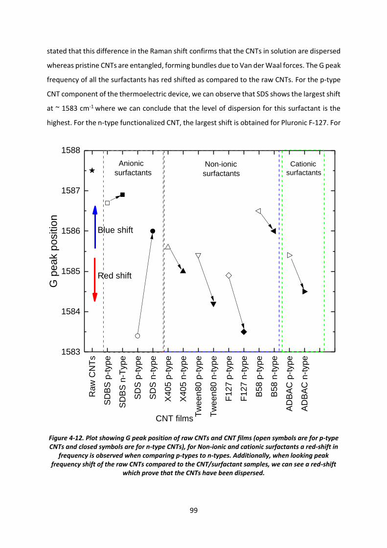
99
stated that this difference in the Raman shift confirms that the CNTs in solution are dispersed
whereas pristine CNTs are entangled, forming bundles due to Van der Waal forces. The G peak
frequency of all the surfactants has red shifted as compared to the raw CNTs. For the p-type
CNT component of the thermoelectric device, we can observe that SDS shows the largest shift
at ~ 1583 cm-1 where we can conclude that the level of dispersion for this surfactant is the
highest. For the n-type functionalized CNT, the largest shift is obtained for Pluronic F-127. For
Figure 4-12. Plot showing G peak position of raw CNTs and CNT films (open symbols are for p-type CNTs and closed symbols are for n-type CNTs), for Non-ionic and cationic surfactants a red-shift in
frequency is observed when comparing p-types to n-types. Additionally, when looking peak frequency shift of the raw CNTs compared to the CNT/surfactant samples, we can see a red-shift
which prove that the CNTs have been dispersed.
Raw
CN
Ts
SD
BS
p-t
yp
e
SD
BS
n-T
yp
e
SD
S p
-typ
e
SD
S n
-typ
e
X40
5 p
-typ
e
X40
5 n
-typ
e
Tw
een
80
p-t
yp
e
Tw
een
80
n-t
yp
e
F1
27
p-t
yp
e
F1
27
n-t
yp
e
B58
p-t
yp
e
B58
n-t
yp
e
AD
BA
C p
-type
AD
BA
C n
-type
1583
1584
1585
1586
1587
1588
Red shift
Cationic
surfactants
Non-ionic
surfactants
Anionic
surfactants
G p
eak p
ositio
n
CNT films
Blue shift
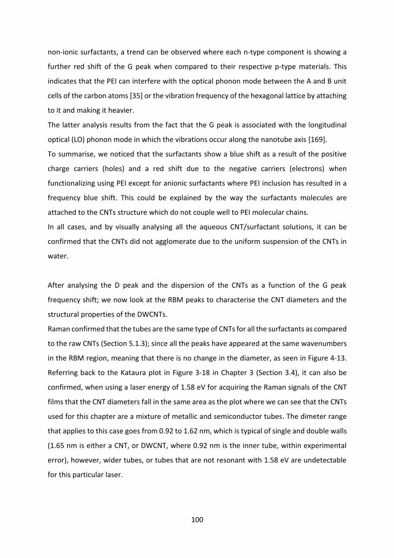
100
non-ionic surfactants, a trend can be observed where each n-type component is showing a
further red shift of the G peak when compared to their respective p-type materials. This
indicates that the PEI can interfere with the optical phonon mode between the A and B unit
cells of the carbon atoms [35] or the vibration frequency of the hexagonal lattice by attaching
to it and making it heavier.
The latter analysis results from the fact that the G peak is associated with the longitudinal
optical (LO) phonon mode in which the vibrations occur along the nanotube axis [169].
To summarise, we noticed that the surfactants show a blue shift as a result of the positive
charge carriers (holes) and a red shift due to the negative carriers (electrons) when
functionalizing using PEI except for anionic surfactants where PEI inclusion has resulted in a
frequency blue shift. This could be explained by the way the surfactants molecules are
attached to the CNTs structure which do not couple well to PEI molecular chains.
In all cases, and by visually analysing all the aqueous CNT/surfactant solutions, it can be
confirmed that the CNTs did not agglomerate due to the uniform suspension of the CNTs in
water.
After analysing the D peak and the dispersion of the CNTs as a function of the G peak
frequency shift; we now look at the RBM peaks to characterise the CNT diameters and the
structural properties of the DWCNTs.
Raman confirmed that the tubes are the same type of CNTs for all the surfactants as compared
to the raw CNTs (Section 5.1.3); since all the peaks have appeared at the same wavenumbers
in the RBM region, meaning that there is no change in the diameter, as seen in Figure 4-13.
Referring back to the Kataura plot in Figure 3-18 in Chapter 3 (Section 3.4), it can also be
confirmed, when using a laser energy of 1.58 eV for acquiring the Raman signals of the CNT
films that the CNT diameters fall in the same area as the plot where we can see that the CNTs
used for this chapter are a mixture of metallic and semiconductor tubes. The dimeter range
that applies to this case goes from 0.92 to 1.62 nm, which is typical of single and double walls
(1.65 nm is either a CNT, or DWCNT, where 0.92 nm is the inner tube, within experimental
error), however, wider tubes, or tubes that are not resonant with 1.58 eV are undetectable
for this particular laser.
101
Figure 4-13. Raman spectra of seven surfactants (both p-type and n-type semiconductors) at the RBM region of the samples aligned against each other shows roughly the same peak positions as
the raw CNTs which indicates that it is the same CNTs coming from the same batch; this is expected because the RBM corresponds to the vibrations in the radial direction of the carbon
atoms, so any functionalization using surfactants happens on the outer shell of the tubes, thus, it should have no impact on the diameter of the CNTs.
Previously, a description was given on the G peak shift which confirmed the efficiency of a
surfactant in dispersing CNTs by showing a red shift when compared to the raw CNTs
wavenumber at 1587 cm-1. In addition to that, the ID/IG ratio of ADBAC p-type was estimated
to be the highest at 0.23 which indicates a higher density of defects. On the other hand, SDBS
p-type was measured to be the lowest ID/IG ratio at 0.1. Therefore, to comprehend potential
reasons for such a difference in CNT quality, a further analysis is required by looking at the
RBM region and more specifically the intensity of each of the Raman signals originating from
the inner and outer walls of the DWCNTs. It is known that peak intensity changes in the RBM
are a consequence of the optical transitions at the density of states [173]. So it was observed
126 168 210 252 294 3360.0
0.2
0.4
Raw CNT
SDBS p-type
SDBS n-type
SDS p-type
SDS n-type
X405 p-type
X405 n-type
Tween80 p-type
Tween80 n-type
F127 p-type
F127 n-type
B58 p-type
B58 n-type
ADBAC p-type
ADBAC n-type
0.92 nm
1.05 nm
1.08 nm
1.21 nm
1.62 nm
Metallic Semiconducting
Inner
CNT wall Outer
CNT wall
Inte
nsity (
a.u
.)
Raman shift (cm-1)
102
from Figure 4-13 that the two most dominant peaks in terms of intensity are the outer wall
(1.62 nm in diameter) and the inner wall (0.92 nm id diameter), this means that the majority
of the CNTs detected by the Raman laser are DWCNTs. Therefore, comparing the ratio of the
inner and outer wall of the DWCNT Raman intensities of each CNT film, we can observe which
CNT shell is more dominant as well as looking at the possible effect of each surfactant as seen
in Figure 4-14. For example, raw DWCNTs display a ratio of ~ 1 where the intensities of both
inner and outer walls are equal; thus, we can use it as a reference point when comparing the
rest of the samples. The most noticeable ratio of 2.5 is for SDBS p-type CNTs, which shows a
higher contribution of the inner wall. This could be correlated with the fact that the quality of
the CNTs found in this sample show a value of 0.1. Consequently, this could mean that the
higher RBM Raman intensity of the inner wall indicates that the outer wall has been
significantly affected whereas the inner wall has remained intact. Furthermore, it is believed
that the strong absorption onto the graphitic surface of SDBS molecules is due to hydrophobic
tail group containing the benzene ring which relies on π-π stacking interaction [158]; this
could potentially mean that the outer DWCNT shell has been damaged. Another reason could
be that the strong π-π bonding has dampened the radial vibrations, reducing the intensity of
the RBM peak. In other words, the surfactant wraps around the outer shell resulting in a
decrease to its vibration amplitude and possibly changing the vibrational energy. On the other
hand, adding PEI, SDBS n-type shows a decrease in the DWCNT walls RBM ratio which means
that the polymer has attached less tightly to the outer shell causing an increase in the outer
wall presence by reducing the number of defects. Another sample to notice is ADBAC p-type
CNTs which has the highest ID/IG ratio, indicating a high number of defects. The inner/outer
wall RBM ratio of 0.57 signifies that the inner wall is more affected than the outer wall. This
could possibly be due to the molecule size of 175 pm where the negatively charged chlorine
molecule can be sucked inside the DWCNT, therefore, an interaction happens with the inner
wall causing defects to its graphite structure. Furthermore, there is a possibility that the high
compression from the surfactant hydrophobic tail is due to the strong binding that dampens
the inner tube.
For non-ionic surfactants, it is observed that there are small variations between the p-type
and n-type at ratios below 1 (except for p-type X-405) which means a stronger interaction
with the outer walls.
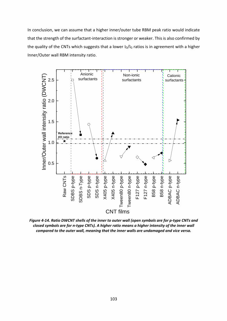
103
In conclusion, we can assume that a higher inner/outer tube RBM peak ratio would indicate
that the strength of the surfactant-interaction is stronger or weaker. This is also confirmed by
the quality of the CNTs which suggests that a lower ID/IG ratios is in agreement with a higher
Inner/Outer wall RBM intensity ratio.
Figure 4-14. Ratio DWCNT shells of the inner to outer wall (open symbols are for p-type CNTs and closed symbols are for n-type CNTs). A higher ratio means a higher intensity of the inner wall
compared to the outer wall, meaning that the inner walls are undamaged and vice versa.
Raw
CN
Ts
SD
BS
p-t
yp
e
SD
BS
n-T
yp
e
SD
S p
-typ
e
SD
S n
-typ
e
X40
5 p
-typ
e
X40
5 n
-typ
e
Tw
een
80
p-t
yp
e
Tw
een
80
n-t
yp
e
F1
27
p-t
yp
e
F1
27
n-t
yp
e
B58
p-t
yp
e
B58
n-t
yp
e
AD
BA
C p
-type
AD
BA
C n
-type
0.5
1.0
1.5
2.0
2.5 Cationic
surfactants
Non-ionic
surfactants
Anionic
surfactants
Reference
I/O ratio
Inner/
Oute
r w
all
inte
nsity r
atio (
DW
CN
T)
CNT films
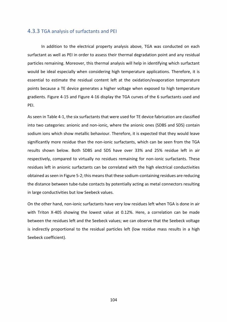
104
4.3.3 TGA analysis of surfactants and PEI
In addition to the electrical property analysis above, TGA was conducted on each
surfactant as well as PEI in order to assess their thermal degradation point and any residual
particles remaining. Moreover, this thermal analysis will help in identifying which surfactant
would be ideal especially when considering high temperature applications. Therefore, it is
essential to estimate the residual content left at the oxidation/evaporation temperature
points because a TE device generates a higher voltage when exposed to high temperature
gradients. Figure 4-15 and Figure 4-16 display the TGA curves of the 6 surfactants used and
PEI.
As seen in Table 4-1, the six surfactants that were used for TE device fabrication are classified
into two categories: anionic and non-ionic, where the anionic ones (SDBS and SDS) contain
sodium ions which show metallic behaviour. Therefore, it is expected that they would leave
significantly more residue than the non-ionic surfactants, which can be seen from the TGA
results shown below. Both SDBS and SDS have over 33% and 25% residue left in air
respectively, compared to virtually no residues remaining for non-ionic surfactants. These
residues left in anionic surfactants can be correlated with the high electrical conductivities
obtained as seen in Figure 5-2; this means that these sodium-containing residues are reducing
the distance between tube-tube contacts by potentially acting as metal connectors resulting
in large conductivities but low Seebeck values.
On the other hand, non-ionic surfactants have very low residues left when TGA is done in air
with Triton X-405 showing the lowest value at 0.12%. Here, a correlation can be made
between the residues left and the Seebeck values; we can observe that the Seebeck voltage
is indirectly proportional to the residual particles left (low residue mass results in a high
Seebeck coefficient).
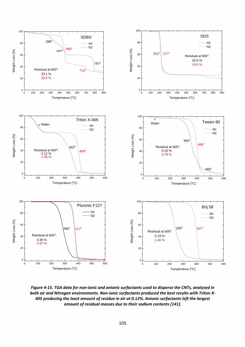
105
Figure 4-15. TGA data for non-ionic and anionic surfactants used to disperse the CNTs, analysed in both air and Nitrogen environments. Non-ionic surfactants produced the best results with Triton X-
405 producing the least amount of residue in air at 0.12%. Anionic surfactants left the largest amount of residual masses due to their sodium contents [141].
0 100 200 300 400 500 600 700 800 9000
20
40
60
80
100
713o
787o
298o
Air
N2
We
igh
t L
oss (
%)
Temperature (oC)
SDBS
Residual at 900o:
33.1 %
29.0 %
460o
447o
0 100 200 300 400 500 600 700 800 9000
20
40
60
80
100
Air
N2
Weig
ht Loss (
%)
Temperature (oC)
SDS
Residual at 900o:
25.5 %
19.0 %
217o211o
0 100 200 300 400 500 600
0
20
40
60
80
100
Air
N2
We
igh
t L
oss (
%)
Temperature (oC)
Triton X-405Water
Residual at 600o:0.12 %1.36 %
362o
409o
0 100 200 300 400 500 600
0
20
40
60
80
100
495o
Air
N2W
eig
ht L
oss (
%)
Temperature (oC)
Tween 80Water
Residual at 600o:0.16 %2.78 %
364o
406o
0 100 200 300 400 500 600
0
20
40
60
80
100
Air
N2
We
igh
t L
oss (
%)
Temperature (oC)
Pluronic F127
Residual at 600o:
0.36 %0.87 %
377o285o
0 100 200 300 400 500 600
0
20
40
60
80
100
Air
N2
We
igh
t L
oss (
%)
Temperature (oC)
Brij 58
Residual at 600o:
0.19 %
1.46 %
407o265o
106
As for PEI, which is the only polymer in this project used to functionalize CNTs into n-type
semiconductors; TGA reveals that at 650 ˚C, there is a very low residual left with 0.27 % in air
and 0.24 % in nitrogen.
Figure 4-16. TGA data analysed in both air and Nitrogen environments for PEI used as a dopant to functionalize dispersed CNTs into n-type semiconductor material.
In summary, it was shown that the non-ionic surfactants are ideal materials for CNT dispersion
due to their low residual content in comparison to the anionic surfactants. However, it is
noted that all the non-ionic surfactants as well as PEI have lower evaporation points
compared to raw CNTs as seen in Figure 4-6 in Section 4.1.4 where the oxidisation
temperature is ~ 590 ˚C. This can be advantageous if the CNTs are needed to be recovered
within a standard oven that doesn’t require a vacuum environment, and thus reducing the
process cost for commercial purposes such as CNT alignment processes [141]. However, in
this situation, if the CNT films were to be used for temperatures higher than that of the
respective evaporation point of the surfactants then this can cause the film to deteriorate
(shrinking) and lose its mechanical integrity causing a short circuit therefore loss of output
power.
0 100 200 300 400 500 600
0
20
40
60
80
100
We
igh
t L
oss (
%)
Temperature (C)
Air
N2
PEI
Residual at 650:
0.27 %
0.24 %
350320
107
Thermoelectric properties of CNT films
After the Raman analysis of the raw CNTs and doped CNTs (p-type and n-type), we
determined the various effects that the surfactants and PEI have on the CNTs, mainly seen
from the shifts in the G peak. Now, we will look at two important ZT parameters, the Seebeck
coefficient (Figure 5-1) and the electrical conductivity (Figure 5-2) measured using the Van
der Pauw technique (Raw data in Appendix B) and the Transmission Line Method.
Thermogravimetric Analysis (TGA) (Figure 4-15 and Figure 4-16) was also performed on the
surfactants in both Nitrogen (N2) and Air in order to determine their thermal degradation
stages and whether any residual masses were left.
During the experimental phase of cutting the CNT films into small dimensions in order to make
TE devices, the cationic surfactant ADBAC did not produce a rectangular film. This is because
the integrity of the film didn’t hold causing it to break apart, therefore no Seebeck voltage
and electrical conductivity values could be obtained.
5.1 Seebeck coefficient and electrical conductivity
From Figure 5-1, the most striking observation to make is the successful conversion of
the p-type CNTs to n-type CNT films after inclusion of PEI. This is seen from the negative
Seebeck values which prove that the majority charge carriers (electrons) have gathered to the
cold end due to thermal diffusion, thus resulting in a negative potential difference. Next, we
notice that the effect of PEI shows that most n-type materials have lower electrical
conductivity values (ranging from 1.0E+03 to 3.6E+03 S/m, see Figure 5-2) than their
respective like-for-like surfactant p-type semiconductors. This is likely caused by the
electrically insulating properties of the polymer resulting in an increase in the distance
between CNTs and in the narrowing of the electronic transport channels causing a reduction
in their conductivity.
Figure 5-2 (b) shows that the TLM method is giving similar results for the conductivity as the
van der Pauw method, and either can be used; however, once metal contacts are deposited
on the film for the TLM method, that film cannot be directly used to manufacture a TE devices,
therefore the van der Pauw method was preferred.
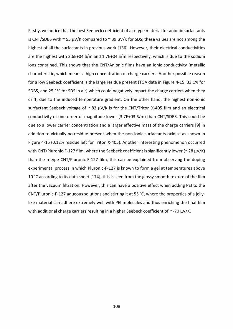
108
Firstly, we notice that the best Seebeck coefficient of a p-type material for anionic surfactants
is CNT/SDBS with ~ 55 µV/K compared to ~ 39 µV/K for SDS; these values are not among the
highest of all the surfactants in previous work [136]. However, their electrical conductivities
are the highest with 2.6E+04 S/m and 1.7E+04 S/m respectively, which is due to the sodium
ions contained. This shows that the CNT/Anionic films have an ionic conductivity (metallic
characteristic, which means a high concentration of charge carriers. Another possible reason
for a low Seebeck coefficient is the large residue present (TGA data in Figure 4-15: 33.1% for
SDBS, and 25.1% for SDS in air) which could negatively impact the charge carriers when they
drift, due to the induced temperature gradient. On the other hand, the highest non-ionic
surfactant Seebeck voltage of ~ 82 µV/K is for the CNT/Triton X-405 film and an electrical
conductivity of one order of magnitude lower (3.7E+03 S/m) than CNT/SDBS. This could be
due to a lower carrier concentration and a larger effective mass of the charge carriers [9] in
addition to virtually no residue present when the non-ionic surfactants oxidise as shown in
Figure 4-15 (0.12% residue left for Triton X-405). Another interesting phenomenon occurred
with CNT/Pluronic-F-127 film, where the Seebeck coefficient is significantly lower (~ 28 µV/K)
than the n-type CNT/Pluronic-F-127 film, this can be explained from observing the doping
experimental process in which Pluronic-F-127 is known to form a gel at temperatures above
10 ˚C according to its data sheet [174]; this is seen from the glossy smooth texture of the film
after the vacuum filtration. However, this can have a positive effect when adding PEI to the
CNT/Pluronic-F-127 aqueous solutions and stirring it at 55 ˚C, where the properties of a jelly-
like material can adhere extremely well with PEI molecules and thus enriching the final film
with additional charge carriers resulting in a higher Seebeck coefficient of ~ -70 µV/K.
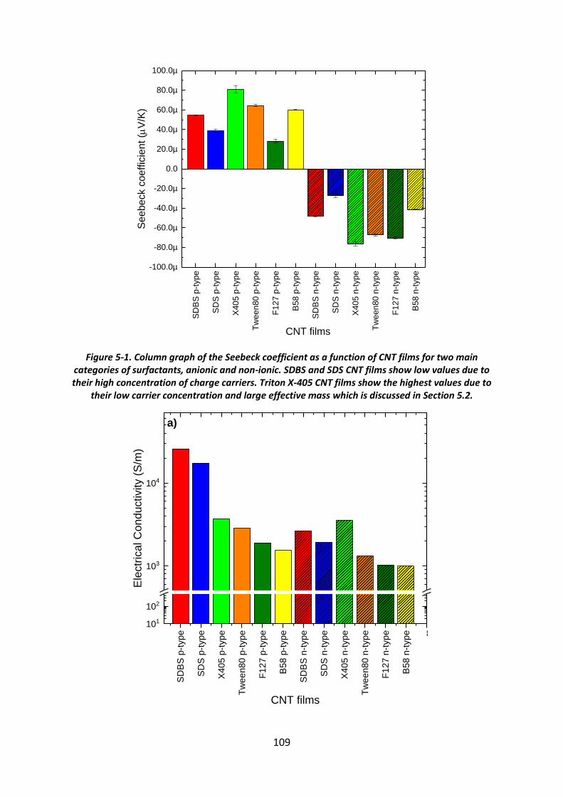
109
Figure 5-1. Column graph of the Seebeck coefficient as a function of CNT films for two main categories of surfactants, anionic and non-ionic. SDBS and SDS CNT films show low values due to their high concentration of charge carriers. Triton X-405 CNT films show the highest values due to
their low carrier concentration and large effective mass which is discussed in Section 5.2.
SD
BS
p-t
yp
e
SD
S p
-typ
e
X405 p
-typ
e
Tw
een80 p
-typ
e
F127
p-t
ype
B58 p
-typ
e
SD
BS
n-t
yp
e
SD
S n
-typ
e
X405 n
-typ
e
Tw
een80 n
-typ
e
F127
n-t
ype
B58 n
-typ
e
-100.0µ
-80.0µ
-60.0µ
-40.0µ
-20.0µ
0.0
20.0µ
40.0µ
60.0µ
80.0µ
100.0µ
Seebeck c
oeffic
ient (
V/K
)
CNT films
SD
BS
p-t
ype
SD
S p
-type
X405 p
-type
Tw
een80 p
-type
F127 p
-type
B58 p
-type
SD
BS
n-t
ype
SD
S n
-type
X405 n
-type
Tw
een80 n
-type
F127 n
-type
B58 n
-type --
101
102
103
104
Ele
ctr
ica
l C
on
du
ctivity (
S/m
)
CNT films
a)
110
Figure 5-2. (a) Column graph of the electrical conductivity (Van der Pauw) as a function of CNT films for two main categories of surfactants, anionic and non-ionic. SDBS and SDS CNT films show the highest values due to their high concentration of charge carriers because of the sodium ions.
All the non-ionic surfactant CNT films show significantly lower values due to their low carrier concentration, (b) shows the comparison between the Van der Pauw method (black bars) and TLM
method (red bars) showing that the TLM line may also be used to estimate the electrical conductivity.
A further aspect of these measurements to analyse is the length of the hydrocarbon chain of
both anionic and non-ionic surfactants; we notice from their chemical structure as seen in
Figure 4-7 that SDBS and SDS contain a hydrophobic chain of 10 hydrocarbons (CH2). On the
other hand, Triton X-405 has the shortest hydrocarbon chain among non-ionic surfactants,
whereas Tween 80 and Pluronic F-127 have the longest chains. In general, there are various
effects of the nature of the hydrophobic group that should be taken into consideration when
interaction between two materials happen (surfactant and CNTs). For example, by increasing
the length of the hydrophobic group, this tends to decrease the solubility of the surfactant in
water and increases its solubility in organic solvents [67]. In addition, it can cause closer
packing of the surfactant molecules at the interface therefore forming micelles.
Consequently, the melting point of the surfactant and of the absorbed film increases.
However, introducing branching into the hydrocarbon chain of a surfactant such as Tween 80
and Pluronic F-127 can contribute in increasing its solubility in water. So in conclusion, the
SD
BS
P-t
ype
SD
S P
-typ
e
X40
5 P
-typ
e
Tw
een
80 P
-type
F1
27 P
-type
B58
P-t
yp
e
SD
BS
N-t
yp
e
SD
S N
-type
X405 N
-typ
e
Tw
een
80
N-t
ype
F1
27
N-t
ype
B58 N
-type --
1E-11
1E-10
1E-9
10
100
1000
10000 Van der Pauw
Transmission Line Measurement
Ele
ctr
ica
l C
on
du
ctivity (
S/m
)
CNT films
b)
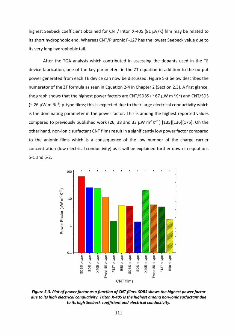
111
highest Seebeck coefficient obtained for CNT/Triton X-405 (81 µV/K) film may be related to
its short hydrophobic end. Whereas CNT/Pluronic F-127 has the lowest Seebeck value due to
its very long hydrophobic tail.
After the TGA analysis which contributed in assessing the dopants used in the TE
device fabrication, one of the key parameters in the ZT equation in addition to the output
power generated from each TE device can now be discussed. Figure 5-3 below describes the
numerator of the ZT formula as seen in Equation 2-4 in Chapter 2 (Section 2.3). A first glance,
the graph shows that the highest power factors are CNT/SDBS (~ 67 μW m-1K-2) and CNT/SDS
(~ 26 μW m-1K-2) p-type films; this is expected due to their large electrical conductivity which
is the dominating parameter in the power factor. This is among the highest reported values
compared to previously published work (26, 38 and 33 μW m-1K-2 ) [135][136][175]. On the
other hand, non-ionic surfactant CNT films result in a significantly low power factor compared
to the anionic films which is a consequence of the low number of the charge carrier
concentration (low electrical conductivity) as it will be explained further down in equations
5-1 and 5-2.
Figure 5-3. Plot of power factor as a function of CNT films. SDBS shows the highest power factor due to its high electrical conductivity. Triton X-405 is the highest among non-ionic surfactant due
to its high Seebeck coefficient and electrical conductivity.
SD
BS
p-t
yp
e
SD
S p
-typ
e
X4
05
p-t
yp
e
Tw
ee
n8
0 p
-typ
e
F1
27
p-t
yp
e
B5
8 p
-typ
e
SD
BS
n-t
yp
e
SD
S n
-typ
e
X4
05
n-t
yp
e
Tw
ee
n8
0 n
-typ
e
F1
27
n-t
yp
e
B5
8 n
-typ
e
0.1
1
10
100
Po
we
r F
acto
r (
W m
-1K
-2 )
CNT films
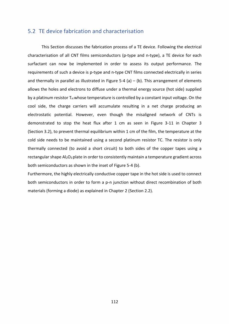
112
5.2 TE device fabrication and characterisation
This Section discusses the fabrication process of a TE device. Following the electrical
characterisation of all CNT films semiconductors (p-type and n-type), a TE device for each
surfactant can now be implemented in order to assess its output performance. The
requirements of such a device is p-type and n-type CNT films connected electrically in series
and thermally in parallel as illustrated in Figure 5-4 (a) – (b). This arrangement of elements
allows the holes and electrons to diffuse under a thermal energy source (hot side) supplied
by a platinum resistor TH whose temperature is controlled by a constant input voltage. On the
cool side, the charge carriers will accumulate resulting in a net charge producing an
electrostatic potential. However, even though the misaligned network of CNTs is
demonstrated to stop the heat flux after 1 cm as seen in Figure 3-11 in Chapter 3
(Section 3.2), to prevent thermal equilibrium within 1 cm of the film, the temperature at the
cold side needs to be maintained using a second platinum resistor TC. The resistor is only
thermally connected (to avoid a short circuit) to both sides of the copper tapes using a
rectangular shape Al2O3 plate in order to consistently maintain a temperature gradient across
both semiconductors as shown in the inset of Figure 5-4 (b).
Furthermore, the highly electrically conductive copper tape in the hot side is used to connect
both semiconductors in order to form a p-n junction without direct recombination of both
materials (forming a diode) as explained in Chapter 2 (Section 2.2).
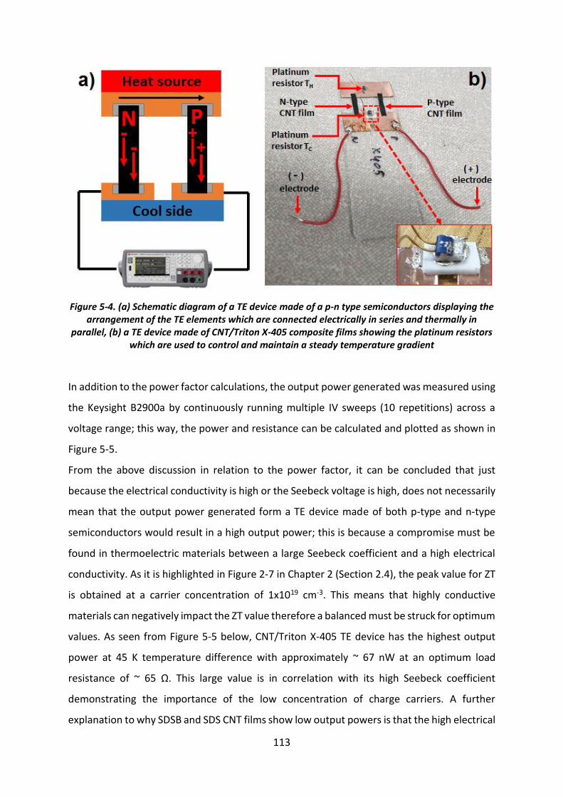
113
Figure 5-4. (a) Schematic diagram of a TE device made of a p-n type semiconductors displaying the arrangement of the TE elements which are connected electrically in series and thermally in
parallel, (b) a TE device made of CNT/Triton X-405 composite films showing the platinum resistors which are used to control and maintain a steady temperature gradient
In addition to the power factor calculations, the output power generated was measured using
the Keysight B2900a by continuously running multiple IV sweeps (10 repetitions) across a
voltage range; this way, the power and resistance can be calculated and plotted as shown in
Figure 5-5.
From the above discussion in relation to the power factor, it can be concluded that just
because the electrical conductivity is high or the Seebeck voltage is high, does not necessarily
mean that the output power generated form a TE device made of both p-type and n-type
semiconductors would result in a high output power; this is because a compromise must be
found in thermoelectric materials between a large Seebeck coefficient and a high electrical
conductivity. As it is highlighted in Figure 2-7 in Chapter 2 (Section 2.4), the peak value for ZT
is obtained at a carrier concentration of 1x1019 cm-3. This means that highly conductive
materials can negatively impact the ZT value therefore a balanced must be struck for optimum
values. As seen from Figure 5-5 below, CNT/Triton X-405 TE device has the highest output
power at 45 K temperature difference with approximately ~ 67 nW at an optimum load
resistance of ~ 65 Ω. This large value is in correlation with its high Seebeck coefficient
demonstrating the importance of the low concentration of charge carriers. A further
explanation to why SDSB and SDS CNT films show low output powers is that the high electrical
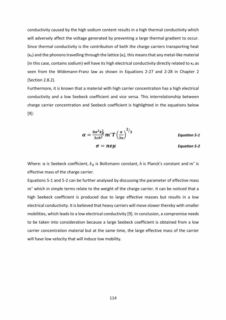
114
conductivity caused by the high sodium content results in a high thermal conductivity which
will adversely affect the voltage generated by preventing a large thermal gradient to occur.
Since thermal conductivity is the contribution of both the charge carriers transporting heat
(κe) and the phonons travelling through the lattice (κl), this means that any metal-like material
(in this case, contains sodium) will have its high electrical conductivity directly related to κe as
seen from the Widemann-Franz law as shown in Equations 2-27 and 2-28 in Chapter 2
(Section 2.8.2).
Furthermore, it is known that a material with high carrier concentration has a high electrical
conductivity and a low Seebeck coefficient and vice versa. This interrelationship between
charge carrier concentration and Seebeck coefficient is highlighted in the equations below
[9]:
𝜶 =𝟖𝝅𝟐𝒌𝑩
𝟐
𝟑𝒆𝒉𝟐𝒎∗𝑻(
𝝅
𝟑𝒏)𝟐
𝟑⁄ Equation 5-1
𝝈 = 𝒏𝒆𝝁 Equation 5-2
Where: α is Seebeck coefficient, 𝑘𝐵 is Boltzmann constant, ℎ is Planck’s constant and 𝑚∗ is
effective mass of the charge carrier.
Equations 5-1 and 5-2 can be further analysed by discussing the parameter of effective mass
𝑚∗ which in simple terms relate to the weight of the charge carrier. It can be noticed that a
high Seebeck coefficient is produced due to large effective masses but results in a low
electrical conductivity. It is believed that heavy carriers will move slower thereby with smaller
mobilities, which leads to a low electrical conductivity [9]. In conclusion, a compromise needs
to be taken into consideration because a large Seebeck coefficient is obtained from a low
carrier concentration material but at the same time, the large effective mass of the carrier
will have low velocity that will induce low mobility.
115
Figure 5-5. A graph displaying the output power for the surfactant CNT films as a function of resistance at a temperature difference of 45 K. The highest value is represented by Triton X-405
due to its high Seebeck coefficient and low residual content.
From the output power data obtained, Triton X-405 has produced the highest value,
therefore, it was compared against other TE devices that have been reported previously as
seen in Table 5-1. From the results obtained in this project, we can observe that our findings
are comparable and competitive in terms of the output power generated which is estimated
to be 1.48 nW/K. To put this value into context, we look at different groups and what has
been achieved. For example, Nonoguchi et al [135] compared 33 compounds which act as
dopants in order to disperse CNTs and add charges to their structure which alters the
electrical properties of the CNT films. It was found that tpp-doped SWCNTs and TCNQ-doped
SWCNTs resulted to a ZT of 0.073 and 1.8 nW/K. This high value could be attributed to a
different chemical structure of the dopants which can strongly bond to the outer structure of
the CNTs, thus, increasing the charge density and the electrical conductivity.
0 50 100 150 200 250 300 350 400 450 5000
10
20
30
40
50
60
70
71
232 176
P (
nW
)
R (Ohm)
X405
SDBS
Tween80
F127
B58
SDS
67
45
86
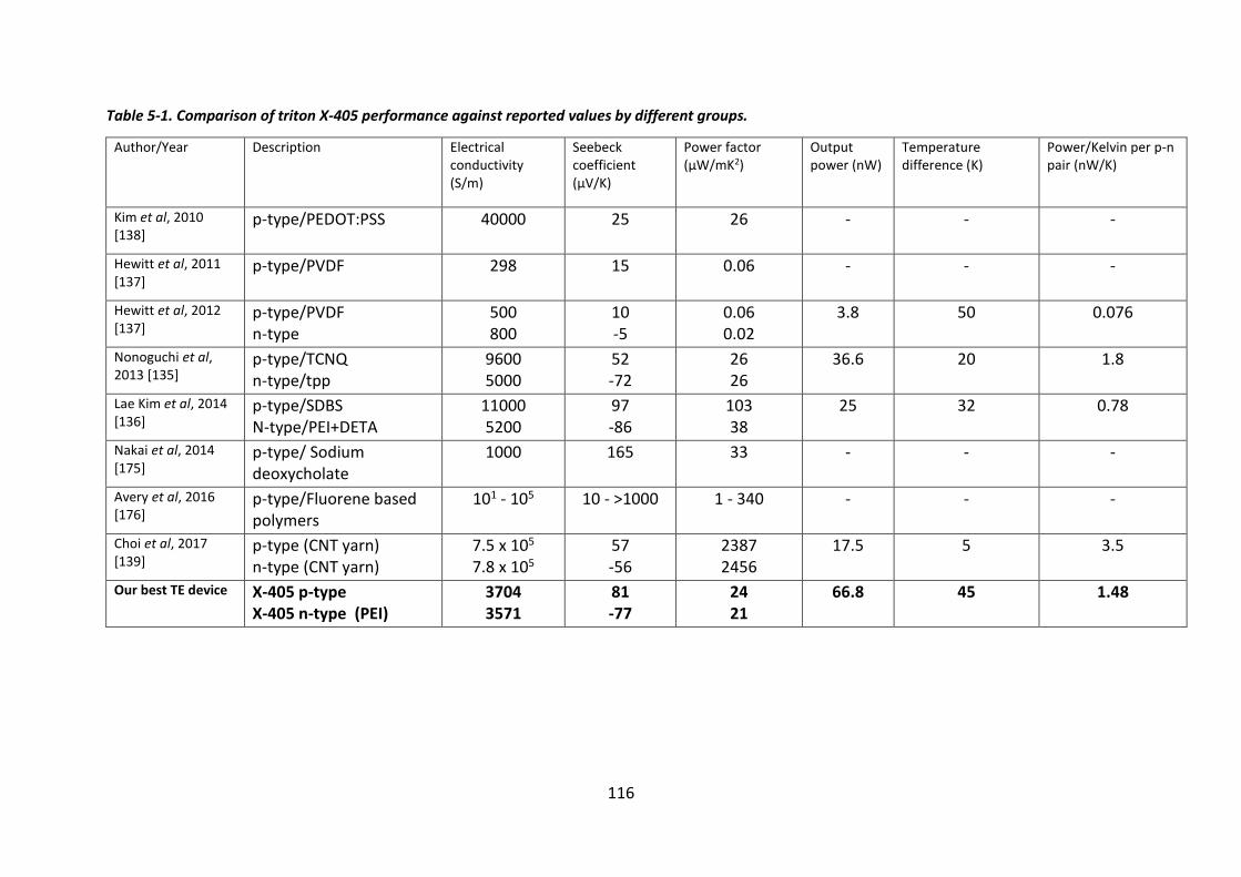
116
Table 5-1. Comparison of triton X-405 performance against reported values by different groups.
Author/Year Description Electrical conductivity (S/m)
Seebeck coefficient (µV/K)
Power factor (µW/mK2)
Output power (nW)
Temperature difference (K)
Power/Kelvin per p-n pair (nW/K)
Kim et al, 2010 [138]
p-type/PEDOT:PSS 40000
25
26
-
-
-
Hewitt et al, 2011 [137]
p-type/PVDF
298
15
0.06
-
-
-
Hewitt et al, 2012 [137]
p-type/PVDF n-type
500 800
10 -5
0.06 0.02
3.8 50 0.076
Nonoguchi et al, 2013 [135]
p-type/TCNQ n-type/tpp
9600 5000
52 -72
26 26
36.6 20 1.8
Lae Kim et al, 2014 [136]
p-type/SDBS N-type/PEI+DETA
11000 5200
97 -86
103 38
25 32 0.78
Nakai et al, 2014 [175]
p-type/ Sodium deoxycholate
1000 165 33 - - -
Avery et al, 2016 [176]
p-type/Fluorene based polymers
101 - 105 10 - >1000 1 - 340 - - -
Choi et al, 2017 [139]
p-type (CNT yarn) n-type (CNT yarn)
7.5 x 10⁵ 7.8 x 10⁵
57 -56
2387 2456
17.5 5 3.5
Our best TE device X-405 p-type X-405 n-type (PEI)
3704 3571
81 -77
24 21
66.8 45 1.48
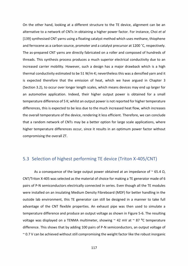
117
On the other hand, looking at a different structure to the TE device, alignment can be an
alternative to a network of CNTs in obtaining a higher power factor. For instance, Choi et al
[139] synthesised CNT yarns using a floating catalyst method which uses methane, thiophene
and ferrocene as a carbon source, promoter and a catalyst precursor at 1200 ˚C, respectively.
The as-prepared CNT yarns are directly fabricated on a roller and composed of hundreds of
threads. This synthesis process produces a much superior electrical conductivity due to an
increased carrier mobility. However, such a design has a major drawback which is a high
thermal conductivity estimated to be 51 W/m·K; nevertheless this was a densified yarn and it
is expected therefore that the emission of heat, which we have argued in Chapter 3
(Section 3.2), to occur over longer length scales, which means devices may end up larger for
an automotive application. Indeed, their higher output power is obtained for a small
temperature difference of 5 K; whilst an output power is not reported for higher temperature
differences, this is expected to be less due to the much increased heat flow, which increases
the overall temperature of the device, rendering it less efficient. Therefore, we can conclude
that a random network of CNTs may be a better option for large scale applications, where
higher temperature differences occur, since it results in an optimum power factor without
compromising the overall ZT.
5.3 Selection of highest performing TE device (Triton X-405/CNT)
As a consequence of the large output power obtained at an impedance of ~ 65.4 Ω,
CNT/Triton X-405 was selected as the material of choice for making a TE generator made of 6
pairs of P-N semiconductors electrically connected in series. Even though all the TE modules
were installed on an insulating Medium Density Fibreboard (MDF) for better handling in the
outside lab environment, this TE generator can still be designed in a manner to take full
advantage of the CNT flexible properties. An exhaust pipe was then used to simulate a
temperature difference and produce an output voltage as shown in Figure 5-6. The resulting
voltage was displayed on a TENMA multimeter, showing ~ 42 mV at ~ 87 ⁰C temperature
difference. This shows that by adding 100 pairs of P-N semiconductors, an output voltage of
~ 0.7 V can be achieved without still compromising the weight factor like the robust inorganic
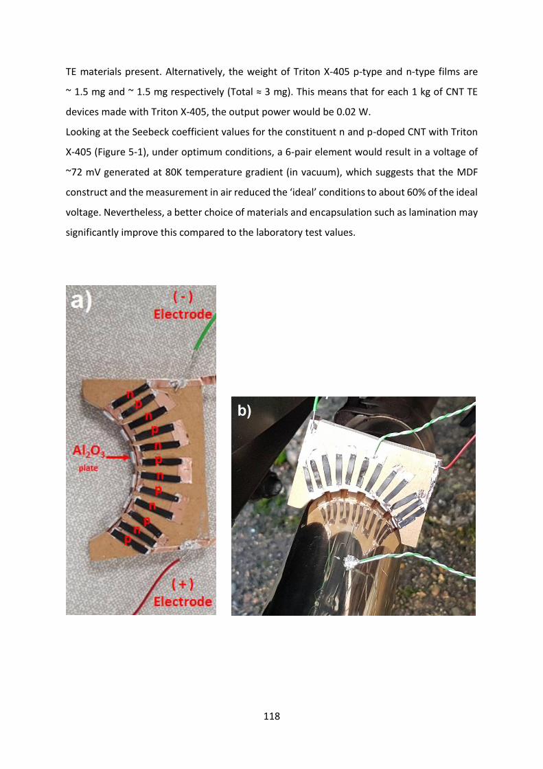
118
TE materials present. Alternatively, the weight of Triton X-405 p-type and n-type films are
~ 1.5 mg and ~ 1.5 mg respectively (Total ≈ 3 mg). This means that for each 1 kg of CNT TE
devices made with Triton X-405, the output power would be 0.02 W.
Looking at the Seebeck coefficient values for the constituent n and p-doped CNT with Triton
X-405 (Figure 5-1), under optimum conditions, a 6-pair element would result in a voltage of
~72 mV generated at 80K temperature gradient (in vacuum), which suggests that the MDF
construct and the measurement in air reduced the ‘ideal’ conditions to about 60% of the ideal
voltage. Nevertheless, a better choice of materials and encapsulation such as lamination may
significantly improve this compared to the laboratory test values.
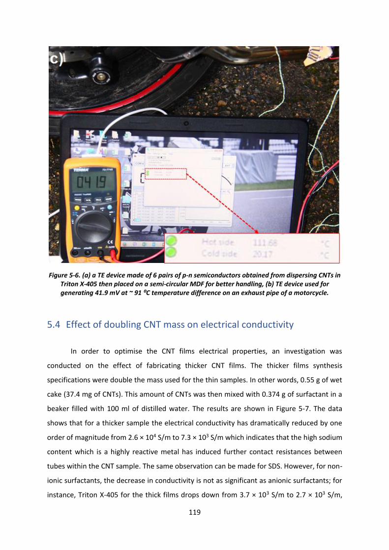
119
Figure 5-6. (a) a TE device made of 6 pairs of p-n semiconductors obtained from dispersing CNTs in Triton X-405 then placed on a semi-circular MDF for better handling, (b) TE device used for generating 41.9 mV at ~ 91 ⁰C temperature difference on an exhaust pipe of a motorcycle.
5.4 Effect of doubling CNT mass on electrical conductivity
In order to optimise the CNT films electrical properties, an investigation was
conducted on the effect of fabricating thicker CNT films. The thicker films synthesis
specifications were double the mass used for the thin samples. In other words, 0.55 g of wet
cake (37.4 mg of CNTs). This amount of CNTs was then mixed with 0.374 g of surfactant in a
beaker filled with 100 ml of distilled water. The results are shown in Figure 5-7. The data
shows that for a thicker sample the electrical conductivity has dramatically reduced by one
order of magnitude from 2.6 × 10⁴ S/m to 7.3 × 10³ S/m which indicates that the high sodium
content which is a highly reactive metal has induced further contact resistances between
tubes within the CNT sample. The same observation can be made for SDS. However, for non-
ionic surfactants, the decrease in conductivity is not as significant as anionic surfactants; for
instance, Triton X-405 for the thick films drops down from 3.7 × 10³ S/m to 2.7 × 10³ S/m,
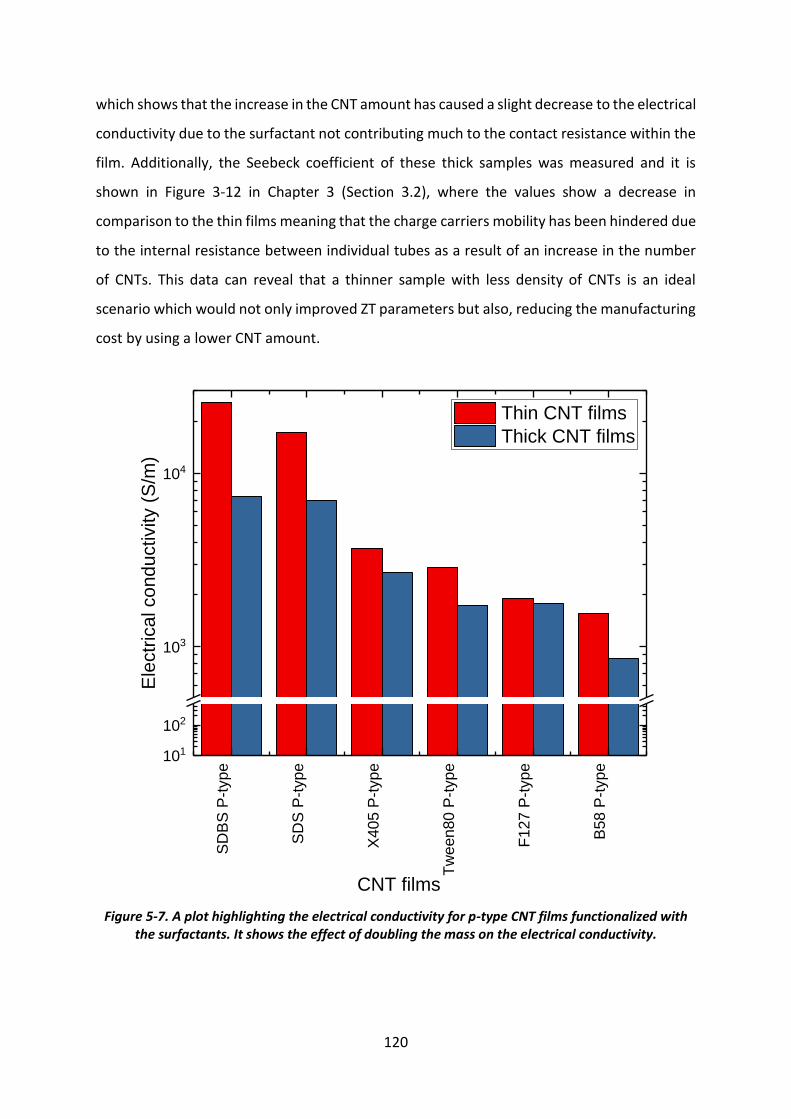
120
which shows that the increase in the CNT amount has caused a slight decrease to the electrical
conductivity due to the surfactant not contributing much to the contact resistance within the
film. Additionally, the Seebeck coefficient of these thick samples was measured and it is
shown in Figure 3-12 in Chapter 3 (Section 3.2), where the values show a decrease in
comparison to the thin films meaning that the charge carriers mobility has been hindered due
to the internal resistance between individual tubes as a result of an increase in the number
of CNTs. This data can reveal that a thinner sample with less density of CNTs is an ideal
scenario which would not only improved ZT parameters but also, reducing the manufacturing
cost by using a lower CNT amount.
Figure 5-7. A plot highlighting the electrical conductivity for p-type CNT films functionalized with the surfactants. It shows the effect of doubling the mass on the electrical conductivity.
SD
BS
P-t
ype
SD
S P
-type
X405 P
-type
Tw
een80 P
-type
F127 P
-type
B58 P
-type
101
102
103
104
Ele
ctr
ica
l co
nd
uctivity (
S/m
)
CNT films
Thin CNT films
Thick CNT films
121
5.5 Summary
In this chapter, we discussed the fabrication of TE devices made of CNTs provided by
Thomas Swan. We first analysed the pristine (raw) CNTs using SEM spectroscopy, Raman and
TGA. This was followed by comparing the effect of seven surfactants from three different
categories (anionic, non-ionic and cationic) used to disperse the CNTs and functionalizing
them by adding PEI. The obtained solution was then vacuum filtered in order to get flat CNT
films. The latter materials were then analysed by Raman which helped in understanding the
effects of surfactants on the outer structure of the CNTs and the efficiency of dispersion.
Furthermore, thermoelectric properties such as the Seebeck coefficient and electrical
conductivity were measured and it was determined that the sodium content in anionic
surfactants contributes positively to get a high electrical conductivity, however, it negatively
impacts the Seebeck coefficient. On the other hand, non-ionic surfactants showed some of
the highest Seebeck values especially Triton X-405 which resulted in a value of 81 µV/K and
an output power of ~ 67 nW at 45 K temperature difference. Due to these high values, Triton
X-405 CNT films were chosen to be the ideal material for the exhaust system application.
Finally, an investigation was conducted on the effect of doubling the CNT content which
showed that the metallic behaviour of SDBS and SDS has contributed to the increase in the
film resistance causing the electrical conductivity to decrease.
122
Conclusion and Future Work
After recognizing the high energy demands of our modern society due to a larger
population compared to the last decade and due to shortage of fossil fuels as well, scientific
institutions have increased their efforts in developing highly efficient advanced materials as
an alternative to current energy sources. These functional materials must meet certain
criteria, such as having a very low environmental impact, high strength, long durability and
low weight. This is why they are becoming increasingly the ideal choice of materials for
modern applications. Therefore, a device that is capable of harvesting waste heat and
converting it into useful electricity is an even better system to investigate. Such material is a
“thermoelectric device” which applies the principal of the Seebeck effect in order to generate
voltage. However, current TE devices available commercially in the market such as those
made of Bi2Te3 are bulky, toxic and expensive to manufacture. This is where CNTs become an
alternative option since they offer many possibilities to alter their thermoelectric parameters;
Seebeck coefficient, electrical and thermal conductivity independently. The low
dimensionality that they offer makes them an attractive material due to the possibility of
inducing quantum effects to affect the phonon transport at the density of states.
CNTs are allotropes of carbon which is in the form of a rolled up sheet of graphene. They can
be s-SWCNTs, m-SWCNTs, DWCNTs or MWCNTs. Each type presents different electronic
characteristics which can be used for various applications. For example, metallic CNTs would
be the perfect candidates for use as electrical connectors, whereas semiconductors can be
used for making TE devices. The use of s-SWCNTs is the best option because they offer the
optimum concentration of charge carriers, which results into the highest power factor along
with an ideal thermal conductivity.
In this thesis, CNT synthesis using the PTCVD technique was explored. This system offers the
option of a low temperature growth process which is beneficial for large scale applications,
as well as vertical alignment. The investigation conducted in Chapter 4 has resulted in a high
quality (ID/IG ratio) of 0.07 and a height of 152 µm.
In chapter 5, TE device fabrication was explored in detail, where the CNTs used were high
quality CNTs provided by Thomas Swan. The Raman characterisation confirmed the high
quality of these CNTs which is 0.15 for raw CNTs.
123
In addition, the fabrication process of TE devices was performed with the use of 7 surfactants
of different hydrophilic group polarity (anionic, non-ionic and cationi(c). The results obtained
for the ZT parameters showed that anionic surfactants have high electrical conductivities due
to their sodium content, but low Seebeck coefficients due to their metallic behaviour, which
leads to a low thermal gradient. On the other hand, non-ionic surfactants exhibited the best
Seebeck coefficient values due to their low concentration of charge carriers.
This led to the selection of Triton X-405 as the ideal surfactant for dispersing the CNTs, thus,
obtaining a thin film with a high power factor and a high output power of 66.9 nW at 45 K
temperature difference.
Finally, all the characterisations carried out on the CNT films have contributed in achieving
the main objective set for this project, which was fabricating a working TE device which can
be used on a motorcycle exhaust and other applications to harvest waste heat.
For future work, it was determined that throughout the characterisations conducted
on the CNTs, there were many examples of further investigations that can be carried out in
order to optimise the ZT parameters.
For instance, the CNTs used in Chapter 5 for the TE device fabrication were characterised by
Raman to be mostly DWCNTs with a mixture of metallic and semiconducting CNTs. Since it is
known theoretically that semiconductors are the ideal type of materials, it is worth exploring
the possibility of reducing the number of metallic CNTs by the use of an electrical breakdown
technique (burning off). This is because the presence of both type of conductors within a film
would result in internal short circuits, therefore reducing the potential voltage generated.
Another area to research is the CNT alignment in a film. This would greatly increase the
electrical conductivity due to low contact resistance at the junctions between the tubes.
However, this could significantly increase the thermal conductivity due to the direct phonon
conduction at the DOS.
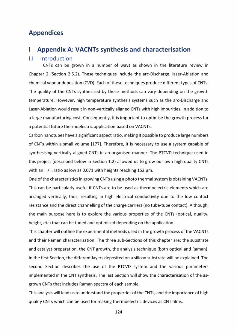
124
Appendices
I Appendix A: VACNTs synthesis and characterisation I.I Introduction CNTs can be grown in a number of ways as shown in the literature review in
Chapter 2 (Section 2.5.2). These techniques include the arc-Discharge, laser-Ablation and
chemical vapour deposition (CVD). Each of these techniques produce different types of CNTs.
The quality of the CNTs synthesised by these methods can vary depending on the growth
temperature. However, high temperature synthesis systems such as the arc-Discharge and
Laser-Ablation would result in non-vertically aligned CNTs with high impurities, in addition to
a large manufacturing cost. Consequently, it is important to optimise the growth process for
a potential future thermoelectric application based on VACNTs.
Carbon nanotubes have a significant aspect ratio, making it possible to produce large numbers
of CNTs within a small volume [177]. Therefore, it is necessary to use a system capable of
synthesising vertically aligned CNTs in an organised manner. The PTCVD technique used in
this project (described below in Section 1.2) allowed us to grow our own high quality CNTs
with an ID/IG ratio as low as 0.071 with heights reaching 152 µm.
One of the characteristics in growing CNTs using a photo thermal system is obtaining VACNTs.
This can be particularly useful if CNTs are to be used as thermoelectric elements which are
arranged vertically, thus, resulting in high electrical conductivity due to the low contact
resistance and the direct channelling of the charge carriers (no tube-tube contact). Although,
the main purpose here is to explore the various properties of the CNTs (optical, quality,
height, etc) that can be tuned and optimised depending on the application.
This chapter will outline the experimental methods used in the growth process of the VACNTs
and their Raman characterisation. The three sub-Sections of this chapter are: the substrate
and catalyst preparation, the CNT growth, the analysis technique (both optical and Raman).
In the first Section, the different layers deposited on a silicon substrate will be explained. The
second Section describes the use of the PTCVD system and the various parameters
implemented in the CNT synthesis. The last Section will show the characterisation of the as-
grown CNTs that includes Raman spectra of each sample.
This analysis will lead us to understand the properties of the CNTs, and the importance of high
quality CNTs which can be used for making thermoelectric devices as CNT films.
125
I.II Description of PTCVD system
In this project, the synthesis of CNTs was performed by photo-thermal chemical vapour
deposition (PTCVD). As reported by Chen et al [49][178], this technique involves the use of
high energy arrays of lamps directed downward on the substrate.
Figure I-1. Schematic diagram of the Photo-thermal CVD system 1000N includes; 8 IR lamps covered by a quartz glass, a substrate holder located above the water cooling line, an inlet for the
reactant gases, and a pump [179].
As noted in Section 2.7.2, different methods for growing CNTs were introduced and discussed.
Conventionally, there are two commonly used methods to grow CNTs which are the catalytic
chemical vapour deposition (CCVD) and the plasma enhanced physical vapour deposition
(PECVD). However, CCVD is a lengthy CNT synthesis technique due to the long process in
reaching the optimum temperature and the time it takes for the chamber to cool down. On
the other hand, PECVD reduces the quality of the CNTs due to the ion bombardment [180].
This happens during the sputtering process by which the substrate holder and the chamber
wall exposed are affected resulting in impurities being deposited into the CNTs. Here, a
different CVD design was adopted for the CNT growth known as photo-thermal CVD (PTCVD)
[49]. The motivation behind this system is its compatibility with CMOS technology and its
ability to grow CNTs over large-areas in excess of 4 inches at industrial scale. Moreover, the
126
capability of synthesising CNTs at low temperatures while maintaining the silicon substrate
below 350 ˚C which was successfully achieved at the ATI by Chen et al [178]. This technology
is based on a top down heating method where the energy is delivered using IR radiations from
the top which will thermally activate the catalyst with the contribution of a carbon source
[179].
This system is equipped with eight infrared (IR) lamps to control the temperature during the
growth process. Figure I-1 shows a schematic of the PTCVD and the various modules which
include: IR lamps installed on the top of the chamber covered and isolated by a quartz
window, a pyrometer which monitors the temperature at the bottom of the substrate (named
TS), inlets and outlets for letting the gases in and for extraction and a water-cooled bottom
plate [179].
In addition, this growth technique can not only deliver heat directly onto a cooled substrate,
it can also produce vertically aligned CNTs which can be used as interconnects in CMOS
technology and other electronic applications where alignment is required. This is achieved by
controlling the formation of the seeds (iron catalyst) during the annealing process. For
example, it has been reported that by Ahmad et al [181] that tuning the thickness of the
Titanium Nitride (TiN) which is defined in the next Section, can result in a desirable catalyst
diameter with a narrow distribution of the CNT. The higher density of the catalyst islands
results in self-organisation of the CNTs into vertically-aligned forests, helped by the
temperature gradient across the CNT (always hotter at the top of the film). This route of
varying the TiN layer thickness has been employed in this work, however, a novel set of gas
ratios is used which resulted in very low CNT quality which hasn’t been reported before.
I.III Preparation of substrate and catalyst
A silicon wafer was used as a substrate for the CNT growth, which is a very common
material for this type of growth. In addition, TiN was employed in order to prevent the catalyst
from diffusing into the silicon and consequently resulting in the formation of noncatalytic
silicide, thus, it serves the purpose of a diffusion barrier [182][183]. As reported by Simmons
et al, due to the increased kinetics, silicide has been shown to inhibit primarily SWCNT growth
which is synthesised at higher temperatures rather than MWCNT [184]. Furthermore,
according to Cao et al, it has been proved that increasing the silicon dioxide layer thickness
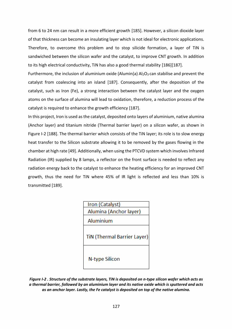
127
from 6 to 24 nm can result in a more efficient growth [185]. However, a silicon dioxide layer
of that thickness can become an insulating layer which is not ideal for electronic applications.
Therefore, to overcome this problem and to stop silicide formation, a layer of TiN is
sandwiched between the silicon wafer and the catalyst, to improve CNT growth. In addition
to its high electrical conductivity, TiN has also a good thermal stability [186][187].
Furthermore, the inclusion of aluminium oxide (Alumin(a) Al2O3 can stabilise and prevent the
catalyst from coalescing into an island [187]. Consequently, after the deposition of the
catalyst, such as Iron (Fe), a strong interaction between the catalyst layer and the oxygen
atoms on the surface of alumina will lead to oxidation, therefore, a reduction process of the
catalyst is required to enhance the growth efficiency [187].
In this project, Iron is used as the catalyst, deposited onto layers of aluminium, native alumina
(Anchor layer) and titanium nitride (Thermal barrier layer) on a silicon wafer, as shown in
Figure I-2 [188]. The thermal barrier which consists of the TiN layer; its role is to slow energy
heat transfer to the Silicon substrate allowing it to be removed by the gases flowing in the
chamber at high rate [49]. Additionally, when using the PTCVD system which involves Infrared
Radiation (IR) supplied by 8 lamps, a reflector on the front surface is needed to reflect any
radiation energy back to the catalyst to enhance the heating efficiency for an improved CNT
growth, thus the need for TiN where 45% of IR light is reflected and less than 10% is
transmitted [189].
Figure I-2 . Structure of the substrate layers, TiN is deposited on n-type silicon wafer which acts as a thermal barrier, followed by an aluminium layer and its native oxide which is sputtered and acts
as an anchor layer. Lastly, the Fe catalyst is deposited on top of the native alumina.
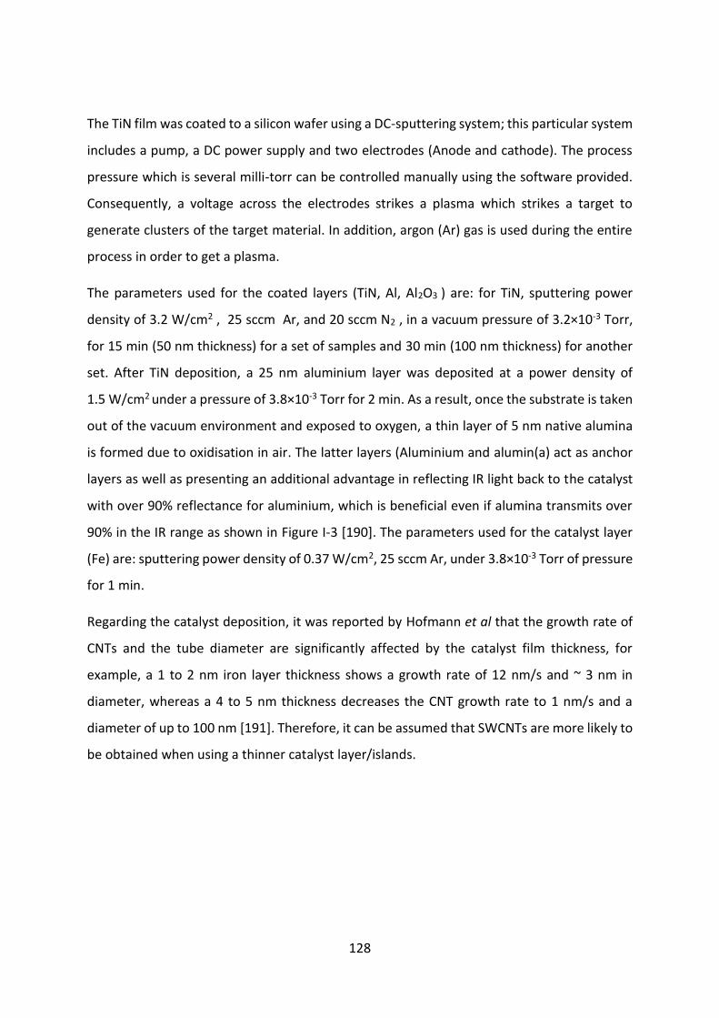
128
The TiN film was coated to a silicon wafer using a DC-sputtering system; this particular system
includes a pump, a DC power supply and two electrodes (Anode and cathode). The process
pressure which is several milli-torr can be controlled manually using the software provided.
Consequently, a voltage across the electrodes strikes a plasma which strikes a target to
generate clusters of the target material. In addition, argon (Ar) gas is used during the entire
process in order to get a plasma.
The parameters used for the coated layers (TiN, Al, Al2O3 ) are: for TiN, sputtering power
density of 3.2 W/cm2 , 25 sccm Ar, and 20 sccm N2 , in a vacuum pressure of 3.2×10⁻³ Torr,
for 15 min (50 nm thickness) for a set of samples and 30 min (100 nm thickness) for another
set. After TiN deposition, a 25 nm aluminium layer was deposited at a power density of
1.5 W/cm2 under a pressure of 3.8×10⁻³ Torr for 2 min. As a result, once the substrate is taken
out of the vacuum environment and exposed to oxygen, a thin layer of 5 nm native alumina
is formed due to oxidisation in air. The latter layers (Aluminium and alumin(a) act as anchor
layers as well as presenting an additional advantage in reflecting IR light back to the catalyst
with over 90% reflectance for aluminium, which is beneficial even if alumina transmits over
90% in the IR range as shown in Figure I-3 [190]. The parameters used for the catalyst layer
(Fe) are: sputtering power density of 0.37 W/cm2, 25 sccm Ar, under 3.8×10⁻³ Torr of pressure
for 1 min.
Regarding the catalyst deposition, it was reported by Hofmann et al that the growth rate of
CNTs and the tube diameter are significantly affected by the catalyst film thickness, for
example, a 1 to 2 nm iron layer thickness shows a growth rate of 12 nm/s and ~ 3 nm in
diameter, whereas a 4 to 5 nm thickness decreases the CNT growth rate to 1 nm/s and a
diameter of up to 100 nm [191]. Therefore, it can be assumed that SWCNTs are more likely to
be obtained when using a thinner catalyst layer/islands.
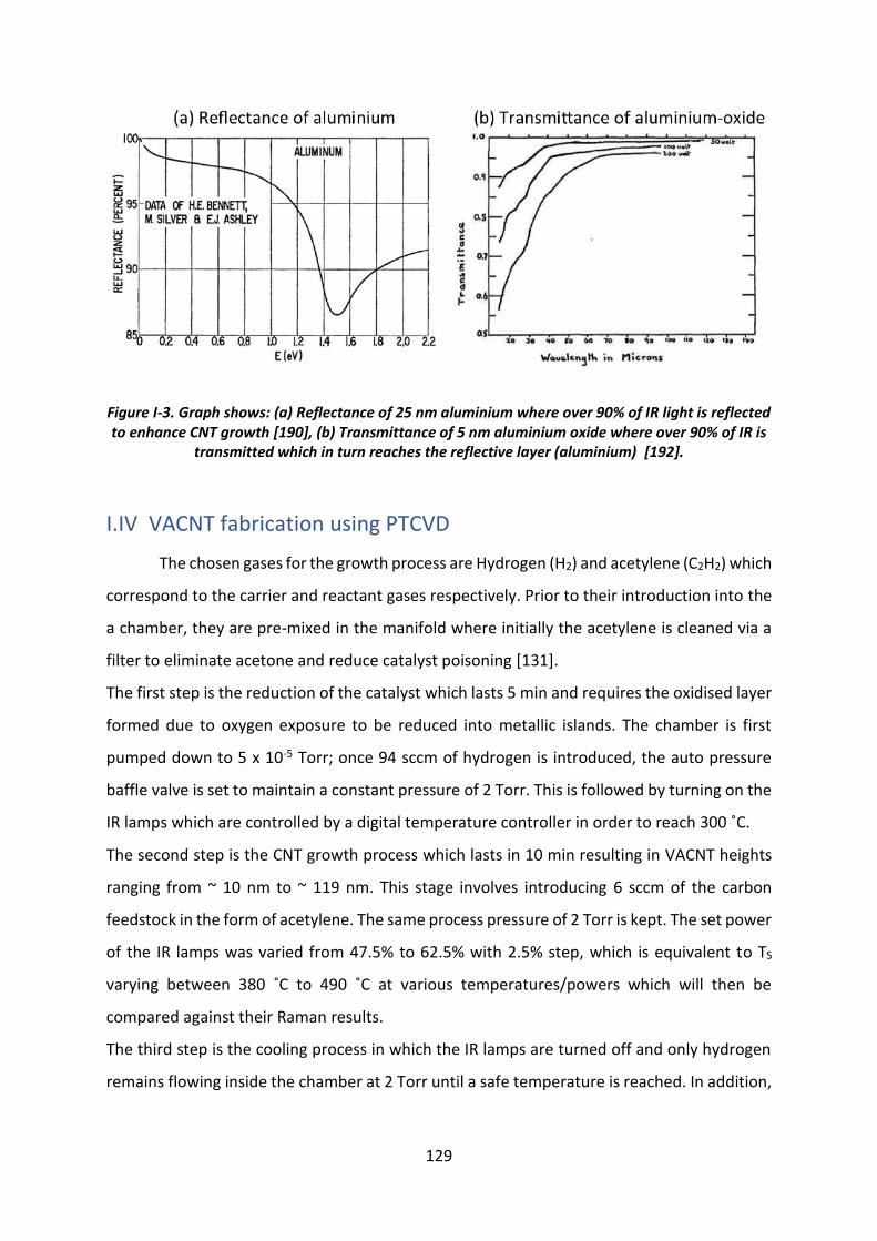
129
Figure I-3. Graph shows: (a) Reflectance of 25 nm aluminium where over 90% of IR light is reflected to enhance CNT growth [190], (b) Transmittance of 5 nm aluminium oxide where over 90% of IR is
transmitted which in turn reaches the reflective layer (aluminium) [192].
I.IV VACNT fabrication using PTCVD
The chosen gases for the growth process are Hydrogen (H2) and acetylene (C2H2) which
correspond to the carrier and reactant gases respectively. Prior to their introduction into the
a chamber, they are pre-mixed in the manifold where initially the acetylene is cleaned via a
filter to eliminate acetone and reduce catalyst poisoning [131].
The first step is the reduction of the catalyst which lasts 5 min and requires the oxidised layer
formed due to oxygen exposure to be reduced into metallic islands. The chamber is first
pumped down to 5 x 10⁻⁵ Torr; once 94 sccm of hydrogen is introduced, the auto pressure
baffle valve is set to maintain a constant pressure of 2 Torr. This is followed by turning on the
IR lamps which are controlled by a digital temperature controller in order to reach 300 ˚C.
The second step is the CNT growth process which lasts in 10 min resulting in VACNT heights
ranging from ~ 10 nm to ~ 119 nm. This stage involves introducing 6 sccm of the carbon
feedstock in the form of acetylene. The same process pressure of 2 Torr is kept. The set power
of the IR lamps was varied from 47.5% to 62.5% with 2.5% step, which is equivalent to TS
varying between 380 ˚C to 490 ˚C at various temperatures/powers which will then be
compared against their Raman results.
The third step is the cooling process in which the IR lamps are turned off and only hydrogen
remains flowing inside the chamber at 2 Torr until a safe temperature is reached. In addition,
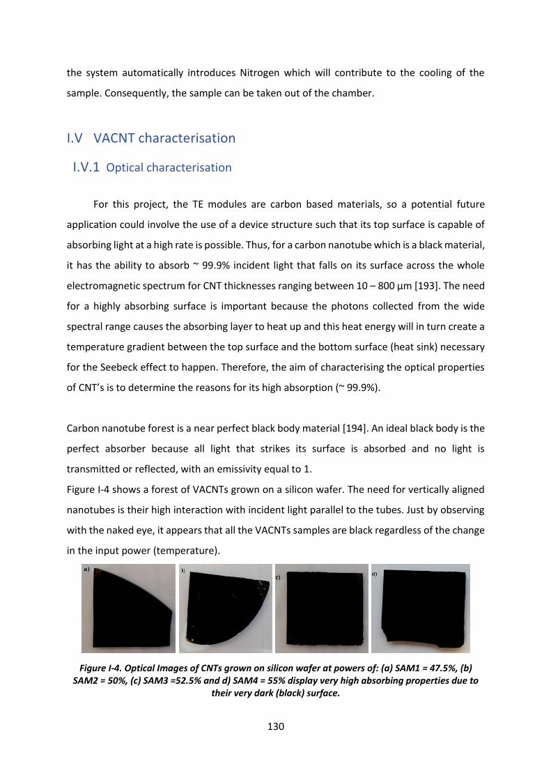
130
the system automatically introduces Nitrogen which will contribute to the cooling of the
sample. Consequently, the sample can be taken out of the chamber.
I.V VACNT characterisation
I.V.1 Optical characterisation
For this project, the TE modules are carbon based materials, so a potential future
application could involve the use of a device structure such that its top surface is capable of
absorbing light at a high rate is possible. Thus, for a carbon nanotube which is a black material,
it has the ability to absorb ~ 99.9% incident light that falls on its surface across the whole
electromagnetic spectrum for CNT thicknesses ranging between 10 – 800 µm [193]. The need
for a highly absorbing surface is important because the photons collected from the wide
spectral range causes the absorbing layer to heat up and this heat energy will in turn create a
temperature gradient between the top surface and the bottom surface (heat sink) necessary
for the Seebeck effect to happen. Therefore, the aim of characterising the optical properties
of CNT’s is to determine the reasons for its high absorption (~ 99.9%).
Carbon nanotube forest is a near perfect black body material [194]. An ideal black body is the
perfect absorber because all light that strikes its surface is absorbed and no light is
transmitted or reflected, with an emissivity equal to 1.
Figure I-4 shows a forest of VACNTs grown on a silicon wafer. The need for vertically aligned
nanotubes is their high interaction with incident light parallel to the tubes. Just by observing
with the naked eye, it appears that all the VACNTs samples are black regardless of the change
in the input power (temperature).
Figure I-4. Optical Images of CNTs grown on silicon wafer at powers of: (a) SAM1 = 47.5%, (b) SAM2 = 50%, (c) SAM3 =52.5% and d) SAM4 = 55% display very high absorbing properties due to
their very dark (black) surface.
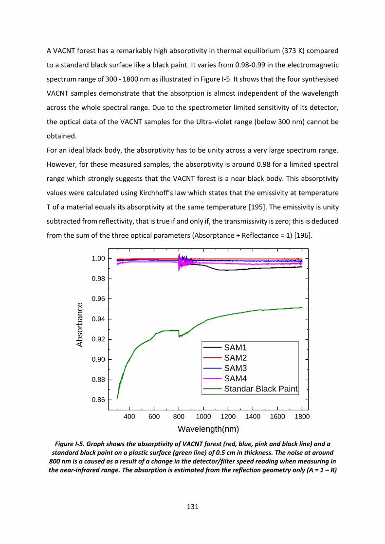
131
A VACNT forest has a remarkably high absorptivity in thermal equilibrium (373 K) compared
to a standard black surface like a black paint. It varies from 0.98-0.99 in the electromagnetic
spectrum range of 300 - 1800 nm as illustrated in Figure I-5. It shows that the four synthesised
VACNT samples demonstrate that the absorption is almost independent of the wavelength
across the whole spectral range. Due to the spectrometer limited sensitivity of its detector,
the optical data of the VACNT samples for the Ultra-violet range (below 300 nm) cannot be
obtained.
For an ideal black body, the absorptivity has to be unity across a very large spectrum range.
However, for these measured samples, the absorptivity is around 0.98 for a limited spectral
range which strongly suggests that the VACNT forest is a near black body. This absorptivity
values were calculated using Kirchhoff’s law which states that the emissivity at temperature
T of a material equals its absorptivity at the same temperature [195]. The emissivity is unity
subtracted from reflectivity, that is true if and only if, the transmissivity is zero; this is deduced
from the sum of the three optical parameters (Absorptance + Reflectance = 1) [196].
400 600 800 1000 1200 1400 1600 1800
0.86
0.88
0.90
0.92
0.94
0.96
0.98
1.00
Ab
so
rban
ce
Wavelength(nm)
SAM1
SAM2
SAM3
SAM4
Standar Black Paint
Figure I-5. Graph shows the absorptivity of VACNT forest (red, blue, pink and black line) and a standard black paint on a plastic surface (green line) of 0.5 cm in thickness. The noise at around
800 nm is a caused as a result of a change in the detector/filter speed reading when measuring in the near-infrared range. The absorption is estimated from the reflection geometry only (A = 1 – R)
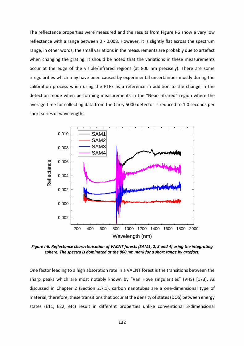
132
The reflectance properties were measured and the results from Figure I-6 show a very low
reflectance with a range between 0 - 0.008. However, it is slightly flat across the spectrum
range, in other words, the small variations in the measurements are probably due to artefact
when changing the grating. It should be noted that the variations in these measurements
occur at the edge of the visible/infrared regions (at 800 nm precisely). There are some
irregularities which may have been caused by experimental uncertainties mostly during the
calibration process when using the PTFE as a reference in addition to the change in the
detection mode when performing measurements in the “Near-infrared” region where the
average time for collecting data from the Carry 5000 detector is reduced to 1.0 seconds per
short series of wavelengths.
200 400 600 800 1000 1200 1400 1600 1800 2000
-0.002
0.000
0.002
0.004
0.006
0.008
0.010
Re
fle
cta
nce
Wavelength (nm)
SAM1
SAM2
SAM3
SAM4
Figure I-6. Reflectance characterisation of VACNT forests (SAM1, 2, 3 and 4) using the integrating sphere. The spectra is dominated at the 800 nm mark for a short range by artefact.
One factor leading to a high absorption rate in a VACNT forest is the transitions between the
sharp peaks which are most notably known by “Van Hove singularities” (VHS) [173]. As
discussed in Chapter 2 (Section 2.7.1), carbon nanotubes are a one-dimensional type of
material, therefore, these transitions that occur at the density of states (DOS) between energy
states (E11, E22, etc) result in different properties unlike conventional 3-dimensional
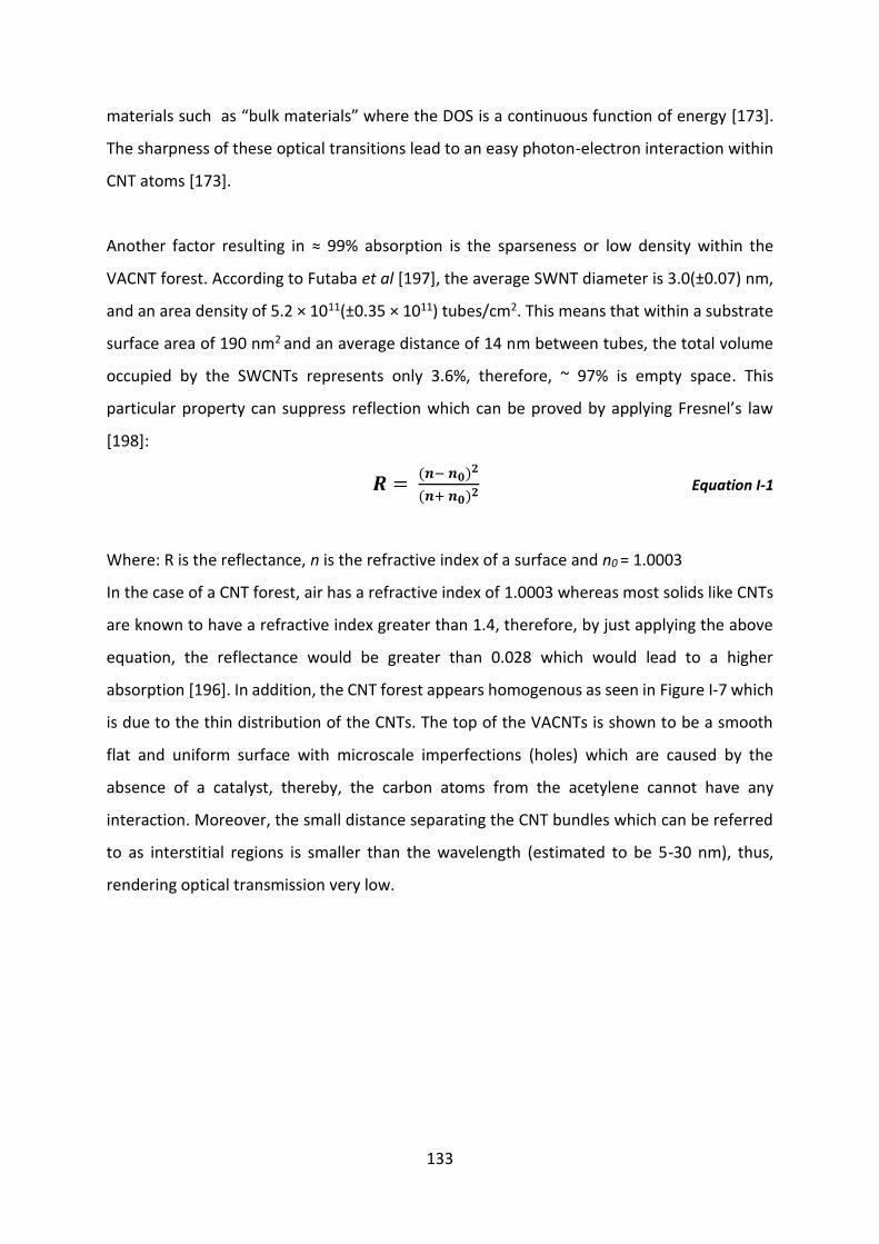
133
materials such as “bulk materials” where the DOS is a continuous function of energy [173].
The sharpness of these optical transitions lead to an easy photon-electron interaction within
CNT atoms [173].
Another factor resulting in ≈ 99% absorption is the sparseness or low density within the
VACNT forest. According to Futaba et al [197], the average SWNT diameter is 3.0(±0.07) nm,
and an area density of 5.2 × 10¹¹(±0.35 × 10¹¹) tubes/cm2. This means that within a substrate
surface area of 190 nm2 and an average distance of 14 nm between tubes, the total volume
occupied by the SWCNTs represents only 3.6%, therefore, ~ 97% is empty space. This
particular property can suppress reflection which can be proved by applying Fresnel’s law
[198]:
𝑹 = (𝒏− 𝒏𝟎)
𝟐
(𝒏+ 𝒏𝟎)𝟐 Equation I-1
Where: R is the reflectance, n is the refractive index of a surface and n0 = 1.0003
In the case of a CNT forest, air has a refractive index of 1.0003 whereas most solids like CNTs
are known to have a refractive index greater than 1.4, therefore, by just applying the above
equation, the reflectance would be greater than 0.028 which would lead to a higher
absorption [196]. In addition, the CNT forest appears homogenous as seen in Figure I-7 which
is due to the thin distribution of the CNTs. The top of the VACNTs is shown to be a smooth
flat and uniform surface with microscale imperfections (holes) which are caused by the
absence of a catalyst, thereby, the carbon atoms from the acetylene cannot have any
interaction. Moreover, the small distance separating the CNT bundles which can be referred
to as interstitial regions is smaller than the wavelength (estimated to be 5-30 nm), thus,
rendering optical transmission very low.
134
Figure I-7. SEM for VACNTs showing a very dense CNT forest closely packed together (bundles) which results in an extremely low reflectance, thus, a higher absorption.
The results presented above are almost similar to those presented by Mizuno et al [196]. The
data presented by the group show that SWCNT have an emissivity of 0.98 - 0.99 across the
UV-far IR.
These properties will benefit TE generators made of VACNTs since a high absorption will
maximise the temperature gradient across a TE device. Our values are close to Surrey
NanoSystems where they have synthesised an extremely dark material (CNTs) called
“Vantablack” which absorbs incident radiation at 99.965% [199].
In conclusion, the above results have proven that vertically aligned carbon nanotubes have
some useful properties for potential future TE devices used as light absorbers, with an
absorptivity close to unity. From an optical point of view, CNTs are black, owing their very low
reflectance and high emissivity to the homogenous sparseness of the VACNT forest in addition
to the uniform alignment structure which is critical in achieving a near black body.
135
I.V.2 Raman characterisation
From Chapter 3.4, a detail description of the Raman technique was provided where
the different peaks associated with a typical Raman CNT signal are shown.
For this Section, the quality of the nanotube will be determined as well as the type of CNTs,
which can be either MWCNT or SWCNT (SWCNT can be either semiconducting or metallic),
using “Raman spectroscopy”. This is particularly important if VACNTs are to be used as
thermoelectric elements, because it a TE device requires both n-type and p-type
semiconductors connected in series, thus, identifying the quality and the type of the CNTs is
necessary.
The experimental work for this Section involves two groups of different thicknesses of
titanium nitride layer, A1 is the set of samples which has 50 nm TiN layer whereas A2 has 100
nm TiN layer. The remaining growth parameters are the same as mentioned in
Section 4.3
For this characterisation, the laser used was ELaser = 2.42 eV which corresponds to λ = 540 nm.
This laser is able to detect both semiconducting (150-210 cm-1) and metallic (210-280 cm-1)
SWCNT in the radial breathing mode (RBM) regions (150-300 cm-1), unlike the red laser with
ELaser = 1.58 eV and λ = 782 nm which can only measure semiconducting SWCNT in the same
region as seen in the Kataura plot in Chapter 3.4 [35] [49][200].
Our CNTs are synthesised using the PTCVD system as described by Shang et al [179]. Before
proceeding to the SEM and Raman data analysis; first, a brief description is given on the
growth model. Baker et al [201], suggested the “Volume diffusion model” which is based on
a top-down heating operating method where the top surface of the iron catalyst is sufficiently
heated to allow the carbon atoms dissociated from the acetylene molecules to interact with
the catalyst islands. Since there is an induced temperature gradient within the catalyst; this
leads the carbon atoms to migrate with high diffusivity to the bottom of the catalyst (colder
side). As a result, the dissociated carbon atoms dissolve and diffuse into the catalyst (Surface
diffusion or bulk diffusion) until a saturated state is reached [202]. A model is shown in
Figure I-8 which was suggested by John Robertson [203].
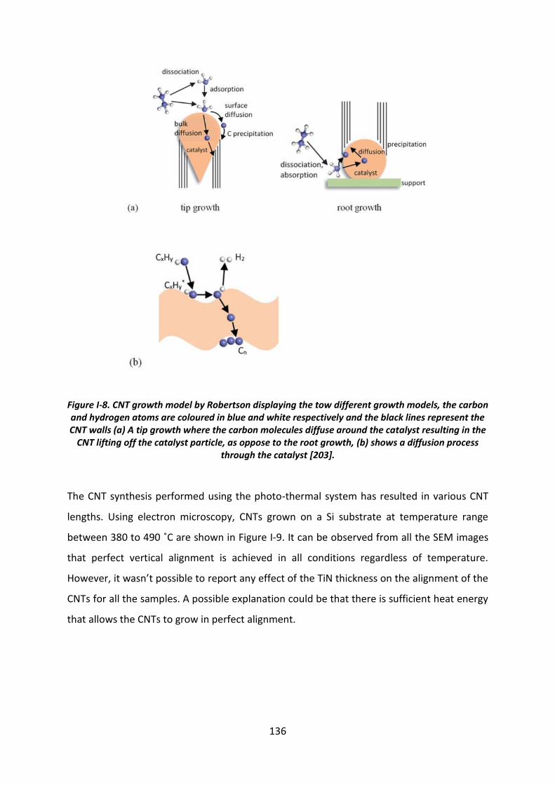
136
Figure I-8. CNT growth model by Robertson displaying the tow different growth models, the carbon and hydrogen atoms are coloured in blue and white respectively and the black lines represent the CNT walls (a) A tip growth where the carbon molecules diffuse around the catalyst resulting in the
CNT lifting off the catalyst particle, as oppose to the root growth, (b) shows a diffusion process through the catalyst [203].
The CNT synthesis performed using the photo-thermal system has resulted in various CNT
lengths. Using electron microscopy, CNTs grown on a Si substrate at temperature range
between 380 to 490 ˚C are shown in Figure I-9. It can be observed from all the SEM images
that perfect vertical alignment is achieved in all conditions regardless of temperature.
However, it wasn’t possible to report any effect of the TiN thickness on the alignment of the
CNTs for all the samples. A possible explanation could be that there is sufficient heat energy
that allows the CNTs to grow in perfect alignment.
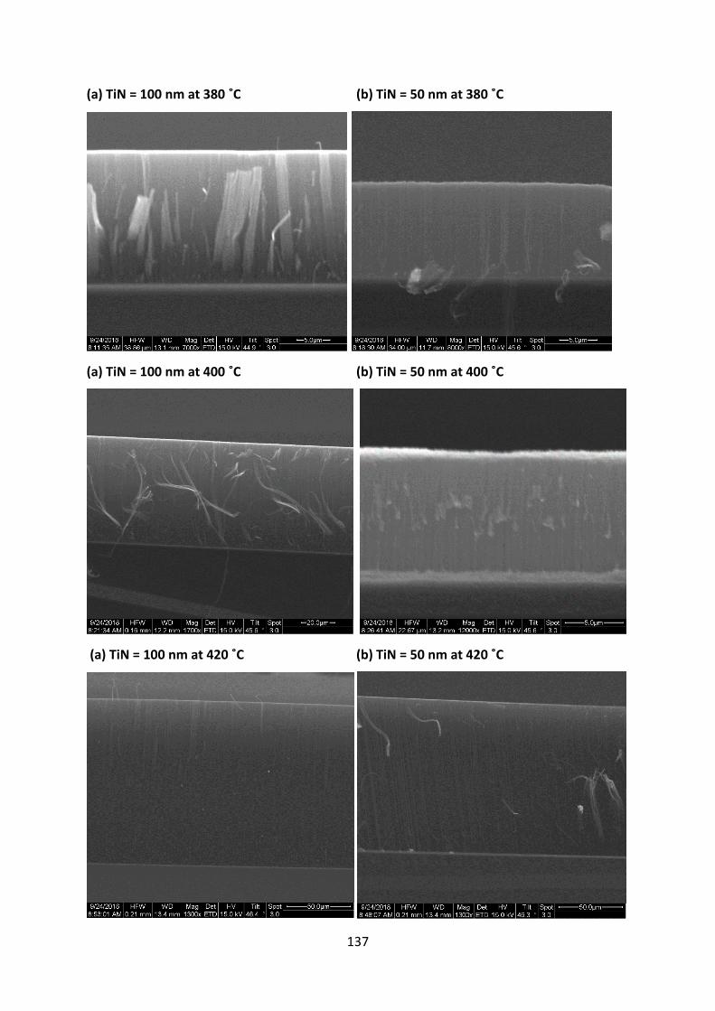
137
(a) TiN = 100 nm at 380 ˚C (b) TiN = 50 nm at 380 ˚C
(a) TiN = 100 nm at 400 ˚C (b) TiN = 50 nm at 400 ˚C
(a) TiN = 100 nm at 420 ˚C (b) TiN = 50 nm at 420 ˚C
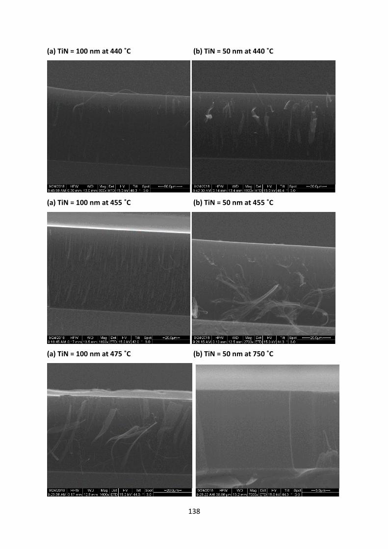
138
(a) TiN = 100 nm at 440 ˚C (b) TiN = 50 nm at 440 ˚C
(a) TiN = 100 nm at 455 ˚C (b) TiN = 50 nm at 455 ˚C
(a) TiN = 100 nm at 475 ˚C (b) TiN = 50 nm at 750 ˚C
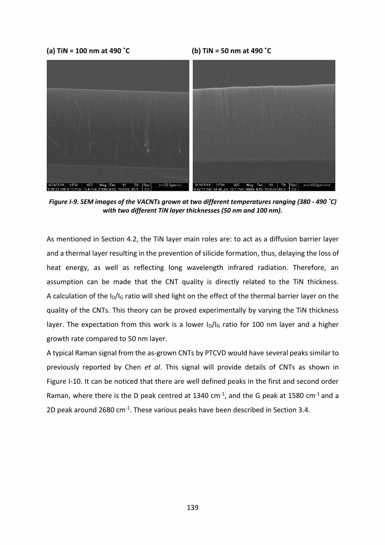
139
(a) TiN = 100 nm at 490 ˚C (b) TiN = 50 nm at 490 ˚C
Figure I-9. SEM images of the VACNTs grown at two different temperatures ranging (380 - 490 ˚C) with two different TiN layer thicknesses (50 nm and 100 nm).
As mentioned in Section 4.2, the TiN layer main roles are: to act as a diffusion barrier layer
and a thermal layer resulting in the prevention of silicide formation, thus, delaying the loss of
heat energy, as well as reflecting long wavelength infrared radiation. Therefore, an
assumption can be made that the CNT quality is directly related to the TiN thickness.
A calculation of the ID/IG ratio will shed light on the effect of the thermal barrier layer on the
quality of the CNTs. This theory can be proved experimentally by varying the TiN thickness
layer. The expectation from this work is a lower ID/IG ratio for 100 nm layer and a higher
growth rate compared to 50 nm layer.
A typical Raman signal from the as-grown CNTs by PTCVD would have several peaks similar to
previously reported by Chen et al. This signal will provide details of CNTs as shown in
Figure I-10. It can be noticed that there are well defined peaks in the first and second order
Raman, where there is the D peak centred at 1340 cm-1, and the G peak at 1580 cm-1 and a
2D peak around 2680 cm-1. These various peaks have been described in Section 3.4.
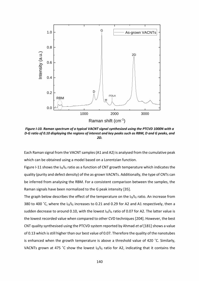
140
Figure I-10. Raman spectrum of a typical VACNT signal synthesized using the PTCVD 1000N with a D-G ratio of 0.10 displaying the regions of interest and key peaks such as RBM, D and G peaks, and
2D.
Each Raman signal from the VACNT samples (A1 and A2) is analysed from the cumulative peak
which can be obtained using a model based on a Lorentzian function.
Figure I-11 shows the ID/IG ratio as a function of CNT growth temperature which indicates the
quality (purity and defect density) of the as-grown VACNTs. Additionally, the type of CNTs can
be inferred from analysing the RBM. For a consistent comparison between the samples, the
Raman signals have been normalized to the G peak intensity [35].
The graph below describes the effect of the temperature on the ID/IG ratio. An increase from
380 to 400 ˚C, where the ID/IG increases to 0.21 and 0.29 for A2 and A1 respectively, then a
sudden decrease to around 0.10, with the lowest ID/IG ratio of 0.07 for A2. The latter value is
the lowest recorded value when compared to other CVD techniques [204]. However, the best
CNT quality synthesised using the PTCVD system reported by Ahmad et al [181] shows a value
of 0.13 which is still higher than our best value of 0.07. Therefore the quality of the nanotubes
is enhanced when the growth temperature is above a threshold value of 420 ˚C. Similarly,
VACNTs grown at 475 ˚C show the lowest ID/IG ratio for A2, indicating that it contains the
1000 2000 3000
0.0
0.2
0.4
0.6
0.8
1.0
2D
iTOLA
M
G
Inte
nsity (
a.u
.)
Raman shift (cm-1)
As-grown VACNTs
RBM
D
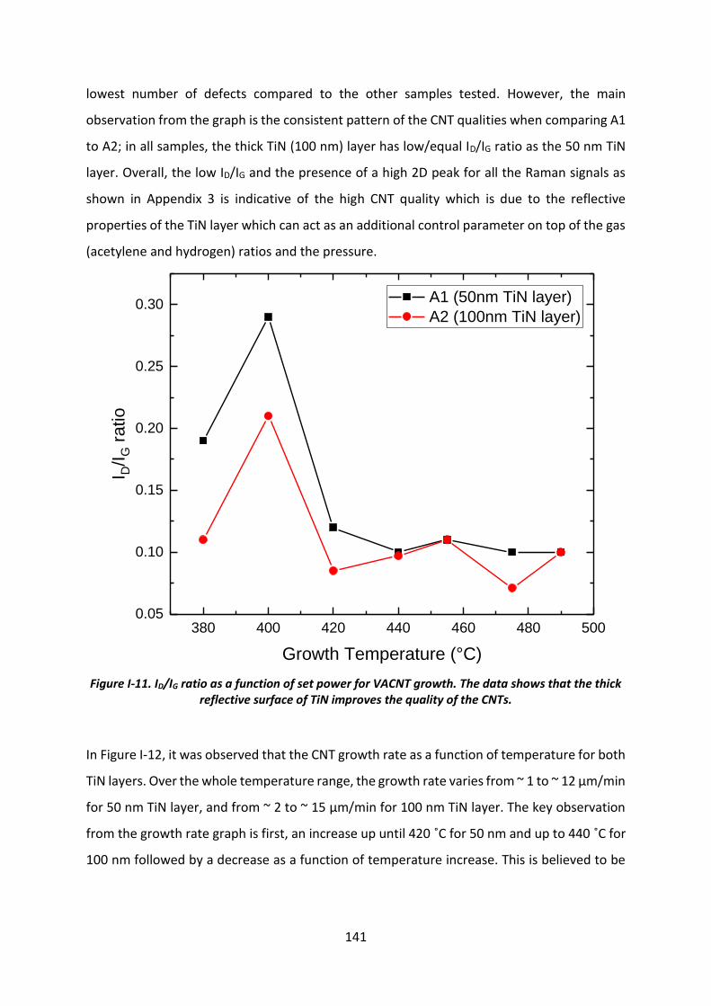
141
lowest number of defects compared to the other samples tested. However, the main
observation from the graph is the consistent pattern of the CNT qualities when comparing A1
to A2; in all samples, the thick TiN (100 nm) layer has low/equal ID/IG ratio as the 50 nm TiN
layer. Overall, the low ID/IG and the presence of a high 2D peak for all the Raman signals as
shown in Appendix 3 is indicative of the high CNT quality which is due to the reflective
properties of the TiN layer which can act as an additional control parameter on top of the gas
(acetylene and hydrogen) ratios and the pressure.
Figure I-11. ID/IG ratio as a function of set power for VACNT growth. The data shows that the thick reflective surface of TiN improves the quality of the CNTs.
In Figure I-12, it was observed that the CNT growth rate as a function of temperature for both
TiN layers. Over the whole temperature range, the growth rate varies from ~ 1 to ~ 12 µm/min
for 50 nm TiN layer, and from ~ 2 to ~ 15 µm/min for 100 nm TiN layer. The key observation
from the growth rate graph is first, an increase up until 420 ˚C for 50 nm and up to 440 ˚C for
100 nm followed by a decrease as a function of temperature increase. This is believed to be
380 400 420 440 460 480 5000.05
0.10
0.15
0.20
0.25
0.30 A1 (50nm TiN layer)
A2 (100nm TiN layer)
I D/I
G r
atio
Growth Temperature (°C)
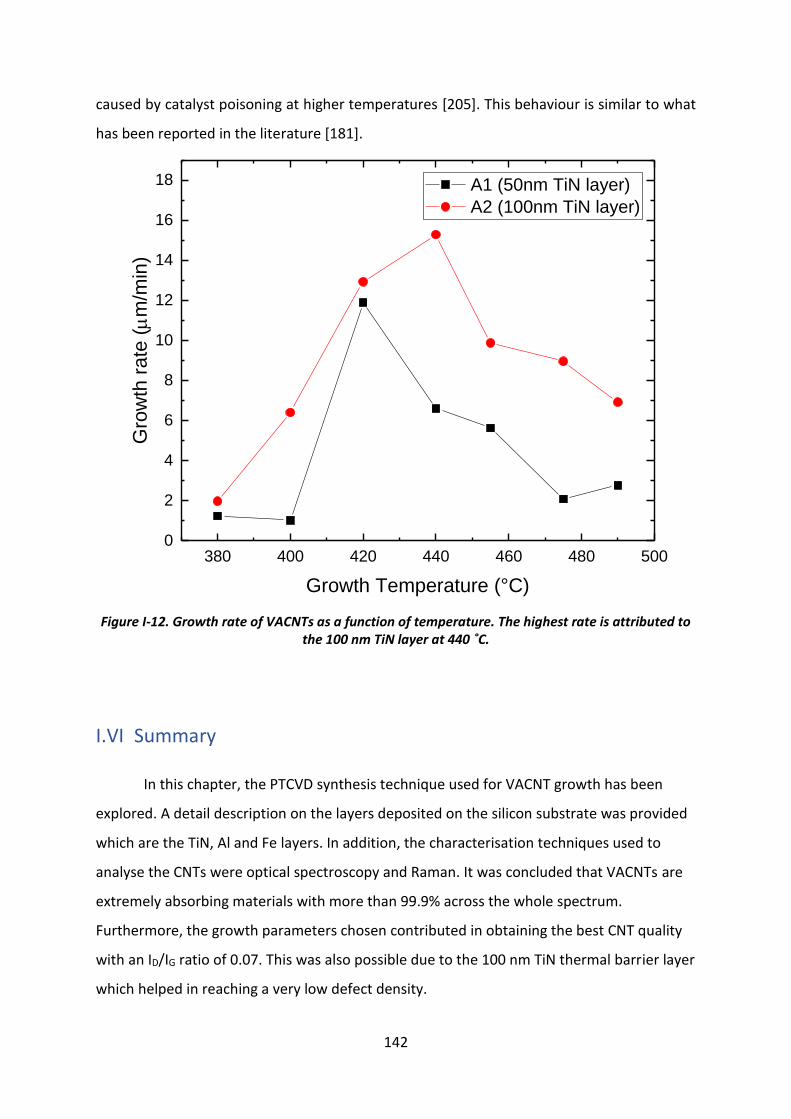
142
caused by catalyst poisoning at higher temperatures [205]. This behaviour is similar to what
has been reported in the literature [181].
Figure I-12. Growth rate of VACNTs as a function of temperature. The highest rate is attributed to the 100 nm TiN layer at 440 ˚C.
I.VI Summary
In this chapter, the PTCVD synthesis technique used for VACNT growth has been
explored. A detail description on the layers deposited on the silicon substrate was provided
which are the TiN, Al and Fe layers. In addition, the characterisation techniques used to
analyse the CNTs were optical spectroscopy and Raman. It was concluded that VACNTs are
extremely absorbing materials with more than 99.9% across the whole spectrum.
Furthermore, the growth parameters chosen contributed in obtaining the best CNT quality
with an ID/IG ratio of 0.07. This was also possible due to the 100 nm TiN thermal barrier layer
which helped in reaching a very low defect density.
380 400 420 440 460 480 5000
2
4
6
8
10
12
14
16
18 A1 (50nm TiN layer)
A2 (100nm TiN layer)
Gro
wth
ra
te (
m/m
in)
Growth Temperature (°C)
143
Finally, even though the PTCVD method presents many advantages in obtaining high quality
CNTs and vertically aligned, there were some challenges that led to not using the as-grown
CNTs, but instead, working on commercial CNTs (Thomas Swan) for the fabrication of the TE
devices. Some of the difficulties include the reliability of the system in producing repeatable
results. On numerous occasions, the system was not able to grow CNTs when using the exact
same parameters and same catalyst conditions. This could well be attributed to many
variables that will make it difficult to identify and fix the problem. Such variables include the
acetylene cylinder which is located outside the building making the reactant gas temperature
variant depending on the season. Also, the build-up of a carbon ash layer on the quartz glass
which separates the IR lamps, thus, altering the intensity of the IR radiation and the ultimate
substrate temperature. This carbon layer could not be cleaned with acetone or isopropanol
(IPA), which means a stronger chemical like and acid may be appropriate, however, for health
and safety reasons, this cannot be done outside a fume cupboard. Furthermore, this system
is used for Diamond-like carbon (DLC) deposition which has caused an unknown layer of
material to be coated on the chamber walls which is easily blown (as dust) when venting the
chamber.
Overall, the process was not as reliable as desired for reproducible growth, and Thomas Swan
CNTs were used instead.
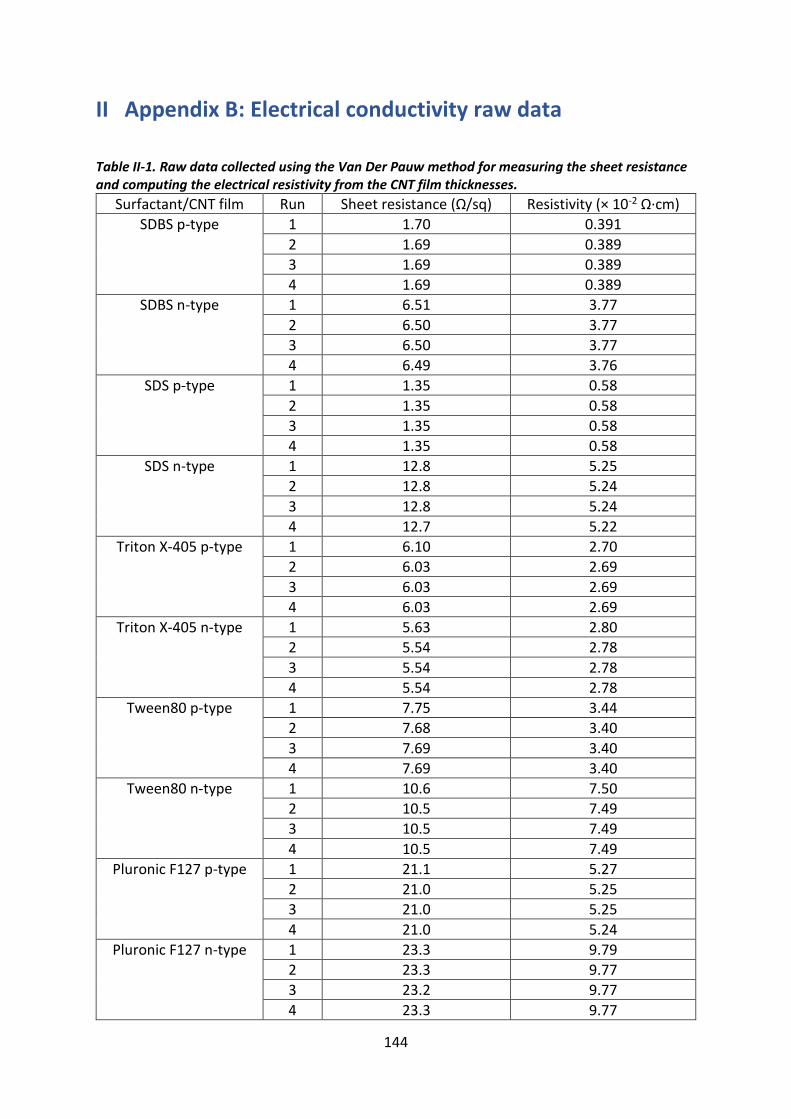
144
II Appendix B: Electrical conductivity raw data
Table II-1. Raw data collected using the Van Der Pauw method for measuring the sheet resistance and computing the electrical resistivity from the CNT film thicknesses.
Surfactant/CNT film Run Sheet resistance (Ω/sq) Resistivity (× 10-2 Ω∙cm)
SDBS p-type 1 1.70 0.391
2 1.69 0.389
3 1.69 0.389
4 1.69 0.389
SDBS n-type 1 6.51 3.77
2 6.50 3.77
3 6.50 3.77
4 6.49 3.76
SDS p-type 1 1.35 0.58
2 1.35 0.58
3 1.35 0.58
4 1.35 0.58
SDS n-type 1 12.8 5.25
2 12.8 5.24
3 12.8 5.24
4 12.7 5.22
Triton X-405 p-type 1 6.10 2.70
2 6.03 2.69
3 6.03 2.69
4 6.03 2.69
Triton X-405 n-type 1 5.63 2.80
2 5.54 2.78
3 5.54 2.78
4 5.54 2.78
Tween80 p-type 1 7.75 3.44
2 7.68 3.40
3 7.69 3.40
4 7.69 3.40
Tween80 n-type 1 10.6 7.50
2 10.5 7.49
3 10.5 7.49
4 10.5 7.49
Pluronic F127 p-type 1 21.1 5.27
2 21.0 5.25
3 21.0 5.25
4 21.0 5.24
Pluronic F127 n-type 1 23.3 9.79
2 23.3 9.77
3 23.2 9.77
4 23.3 9.77
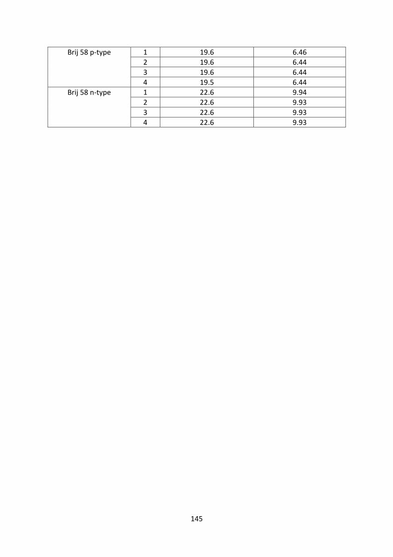
145
Brij 58 p-type 1 19.6 6.46
2 19.6 6.44
3 19.6 6.44
4 19.5 6.44
Brij 58 n-type 1 22.6 9.94
2 22.6 9.93
3 22.6 9.93
4 22.6 9.93
146
References
[1] H. J. Goldsmid, Introduction to Thermoelectricity, 9th ed. Springer, 2010.
[2] X. Zhang and L.-D. Zhao, “Thermoelectric materials: Energy conversion between heat
and electricity,” Journal of Materiomics, vol. 1, no. 2. pp. 92–105, 2015.
[3] Z. B. Tang, Y. D. Deng, C. Q. Su, W. W. Shuai, and C. J. Xie, “A research on
thermoelectric generator’s electrical performance under temperature mismatch
conditions for automotive waste heat recovery system,” Case Stud. Therm. Eng., vol.
5, pp. 143–150, 2015.
[4] C. Yu and K. T. Chau, “Thermoelectric automotive waste heat energy recovery using
maximum power point tracking,” Energy Convers. Manag., vol. 50, no. 6, pp. 1506–
1512, 2009.
[5] “Waste heat to electricity.” [Online]. Available:
https://www.flickr.com/photos/oregonstateuniversity/6152696629/. [Accessed: 15-
Apr-2018].
[6] M. Saleemi, M. S. Toprak, S. Li, M. Johnsson, and M. Muhammed, “Synthesis,
processing, and thermoelectric properties of bulk nanostructured bismuth telluride
(Bi2Te3),” J. Mater. Chem., vol. 22, p. 725, 2012.
[7] N. Toshima, “Recent progress of organic and hybrid thermoelectric materials,” Synth.
Met., vol. 225, pp. 3–21, 2017.
[8] M. S. Dresselhaus et al., “New directions for low-dimensional thermoelectric
materials,” Adv. Mater., vol. 19, pp. 1043–1053, 2007.
[9] G. J. Snyder and E. S. Toberer, “Complex thermoelectric materials.,” Nat. Mater., vol.
7, no. February, pp. 105–114, 2008.
[10] F. Suarez, A. Nozariasbmarz, D. Vashaee, and M. C. Öztürk, “Designing thermoelectric
generators for self-powered wearable electronics,” Energy Environ. Sci., vol. 9, no. 6,
pp. 2099–2113, 2016.
[11] “Harvesting heat from the human body,” in www.idtechex.com, 2017.
147
[12] J. R. Sootsman, D. Y. Chung, and M. G. Kanatzidis, “New and old concepts in
thermoelectric materials,” Angew. Chemie - Int. Ed., vol. 48, pp. 8616–8639, 2009.
[13] P. R. Bandaru, “Electrical properties and applications of carbon nanotube structures.,”
J. Nanosci. Nanotechnol., vol. 7, no. 3, pp. 1239–1267, 2007.
[14] P. Bilalis, D. Katsigiannopoulos, A. Avgeropoulos, and G. Sakellariou, “Non-covalent
functionalization of carbon nanotubes with polymers,” RSC Adv., vol. 4, no. 6, pp.
2911–2934, 2014.
[15] D. M. Rowe, “Thermoelectric Generators,” in Advances in Electronic Ceramics II, vol.
30, Wiley, 2010, pp. 217–225.
[16] D.M. Rowe, “Section I,” in Thermoelectrics Handbook Macro to Nano, CRC Press,
2005, pp. 5–6.
[17] H. J. Goldsmid, Applications of Thermoelectricity. Methuen and Co., 1960.
[18] J.-C. Zheng, “Recent advances on thermoelectric materials,” Front. Phys. China, vol. 3,
no. 3, p. 12, 2011.
[19] Peter Y. Yu author, Fundamentals of Semiconductors Physics and Materials Properties.
Springer, 2010.
[20] C. Kittel and P. McEuen, Introduction to solid state physics, 8th ed. Wiley, 2005.
[21] Haynes William M, CRC Handbook of Chemistry and Physics, 92nd ed. CRC Press,
2011.
[22] H. Scherrer and S. Scherrer, “Section III,” in Thermoelectrics Handbook Macro to
Nano, D.M. Rowe, Ed. CRC Press, 2005.
[23] C. B. Satterthwaite and R. W. J. Ure, “Electrical and thermal properties of Bi2Te3,”
Phys. Rev., vol. 108, pp. 1164–1170, 1957.
[24] T. M. Tritt and M. A. Subramanian, “Thermoelectric Materials , Phenomena, and
Applications: A Bird’s Eye View,” Harvest. Energy through Thermoelectr. Power Gener.
Cool., vol. 31, no. 3, 2006.
[25] H. J. Goldsmith, A. R. Sheard, and D. A. Wright, “The performance of bismuth telluride
148
thermojunctions The performance of bismuth telluride thermojunctions,” Biritish J.
Appl. Phys., vol. 9, pp. 365–370, 1958.
[26] T. C. Harman, P. J. Taylor, M. P. Walsh, and B. E. LaForge, “Quantum dot superlattice
thermoelectric materials and devices.,” Science, vol. 297, no. September, pp. 2229–
2232, 2002.
[27] R. Venkatasubramanian, E. Siivola, T. Colpitts, and B. O’Quinn, “Thin-film
thermoelectric devices with high room-temperature figures of merit.,” Nature, vol.
413, pp. 597–602, 2001.
[28] L. D. Hicks, T. C. Harman, X. Sun, and M. S. Dresselhaus, “Experimental study of the
effect of quantum-well structures on the\nthermoelectric figure of merit,” Fifteenth
Int. Conf. Thermoelectr. Proc. ICT ’96, vol. 53, no. 16, pp. 493–496, 1996.
[29] L.-D. Zhao et al., “Ultralow thermal conductivity and high thermoelectric figure of
merit in SnSe crystals.,” Nature, vol. 508, no. 7496, pp. 373–7, 2014.
[30] G. Chen, M. S. Dresselhaus, G. Dresselhaus, J.-P. Fleurial, and T. Caillat, “Recent
developments in thermoelectric materials,” in Thermoelectrics Handbook Macro to
Nano, vol. 48, CRC Press, 2003, pp. 45–66.
[31] R. B. Weisman and S. Subramoney, “Carbon Nanotubes,” Electrochem. Soc. Interface,
vol. 30, no. 15, pp. 42–46, 2006.
[32] S. Iijima, “Helical microtubules of graphitic carbon,” Nature, vol. 354, pp. 56–58,
1991.
[33] S. Bellucci, “Carbon nanotubes: physics and applications,” Phys. Status Solidi, vol. 2,
no. 1, pp. 34–47, 2005.
[34] H. Dai, “Carbon Nanotubes : Synthesis , Integration , and Properties,” Acc. Chem. Res.,
vol. 35, pp. 1035–1044, 2002.
[35] M. S. Dresselhaus, G. Dresselhaus, R. Saito, and a. Jorio, “Raman spectroscopy of
carbon nanotubes,” Phys. Rep., vol. 409, pp. 47–99, 2005.
[36] E. T. Thostenson, Z. Ren, and T.-W. Chou, “Advances in the science and technology of
carbon nanotubes and their composites: a review,” Compos. Sci. Technol., vol. 61, pp.
149
1899–1912, 2001.
[37] T. Guo, P. Nikolaev, A. Thess, D. T. Colbert, and R. E. Smalley, “Catalytic growth of
single-walled manotubes by laser vaporization,” Chemical Physics Letters, vol. 243,
no. 1–2. pp. 49–54, 1995.
[38] J. Fischer et al., “Metallic resistivity in crystalline ropes of single-wall carbon
nanotubes,” Physical Review B - Condensed Matter and Materials Physics, vol. 55, no.
8. pp. R4921–R4924, 1997.
[39] J. Chrzanowska et al., “Synthesis of carbon nanotubes by the laser ablation method:
Effect of laser wavelength,” Phys. Status Solidi, vol. 252, no. 8, pp. 1860–1867, 2015.
[40] A. Eatemadi et al., “Carbon nanotubes: properties, synthesis, purification, and
medical applications,” Nanoscale Res. Lett., vol. 9, no. 1, p. 393, 2014.
[41] S. Iijima and T. Ichihashi, “Single-shell carbon nanotubes of 1-nm diameter,” Nature,
vol. 363, no. 6430, pp. 603–605, 1993.
[42] D. S. Bethune et al., “Cobalt-catalysed growth of carbon nanotubes with single-
atomic-layer walls,” Nature, vol. 363, no. 6430, pp. 605–607, 1993.
[43] V. N. Popov, “Carbon nanotubes: Properties and application,” Materials Science and
Engineering R: Reports, vol. 43, no. 3. pp. 61–102, 2004.
[44] J. T. H. Tsai, J. S. Chen, and C. L. Sun, “Fabrication of flat capped carbon nanotubes
using an arc-discharge method assisted with a Sm-Co catalyst,” J. Mater. Sci. Mater.
Electron., vol. 22, no. 9, pp. 1387–1392, 2011.
[45] N. Arora and N. N. Sharma, “Arc discharge synthesis of carbon nanotubes:
Comprehensive review,” Diamond and Related Materials, vol. 50. pp. 135–150, 2014.
[46] M. José-Yacamán, M. Miki-Yoshida, L. Rendón, and J. G. Santiesteban, “Catalytic
growth of carbon microtubules with fullerene structure,” Appl. Phys. Lett., vol. 62, no.
6, pp. 657–659, 1993.
[47] M. Kumar and Y. Ando, “Chemical Vapor Deposition of Carbon Nanotubes: A Review
on Growth Mechanism and Mass Production,” J. Nanosci. Nanotechnol., vol. 10, no. 6,
pp. 3739–3758, 2010.
150
[48] S. Roy, R. Bajpai, N. Soin, S. S. Roy, J. A. McLaughlin, and D. S. Misra, “Diameter
control of single wall carbon nanotubes synthesized using chemical vapor
deposition,” Applied Surface Science, vol. 321. pp. 70–79, 2014.
[49] J.-S. Chen, V. Stolojan, and S. R. P. Silva, “Towards type-selective carbon nanotube
growth at low substrate temperature via photo-thermal chemical vapour deposition,”
Carbon N. Y., vol. 84, pp. 409–418, 2015.
[50] M. Terrones, “Science and Technology of the Twenty-First Century: Synthesis,
Properties, and Applications of Carbon Nanotubes,” Annu. Rev. Mater. Res., vol. 33,
no. 1, pp. 419–501, 2003.
[51] V. Sivakumar, A. R. Mohamed, A. Z. Abdullah, and S. P. Chai, “Role of reaction and
factors of carbon nanotubes growth in chemical vapour decomposition process using
Methane-A highlight,” J. Nanomater., vol. 2010, pp. 1–11, 2010.
[52] Y. L. Li, I. A. Kinloch, M. S. P. Shaffer, J. Geng, B. Johnson, and A. H. Windle, “Synthesis
of single-walled carbon nanotubes by a fluidized-bed method,” Chemical Physics
Letters, vol. 384, no. 1–3. pp. 98–102, 2004.
[53] J. Kong, A. M. Cassell, and H. Dai, “Chemical vapor deposition of methane for single-
walled carbon nanotubes,” Chem. Phys. Lett., vol. 292, no. 4–6, pp. 567–574, 1998.
[54] K. Hata, D. N. Futaba, K. Mizuno, T. Namai, M. Yumura, and S. Iijima, “Water-assisted
highly efficient synthesis of impurity-free single-walled carbon nanotubes.,” Science,
vol. 306, pp. 1362–1364, 2004.
[55] C. T. White and T. N. Todorov, “Carbon nanotubes as long ballistic conductors,”
Nature, vol. 393, no. 6682, pp. 240–241, 1998.
[56] T. Dürkop, S. A. Getty, E. Cobas, and M. S. Fuhrer, “Extraordinary Mobility in
Semiconducting Carbon Nanotubes,” Nano Lett., vol. 4, no. 1, pp. 35–39, 2004.
[57] A. Javey, J. Guo, Q. Wang, M. Lundstrom, and H. Dai, “Ballistic carbon nanotube field-
effect transistors,” Nature, vol. 424, no. 6949, pp. 654–657, 2003.
[58] M. M. J. Treacy, T. W. Ebbesen, and J. M. Gibson, “Exceptionally high Young’s
modulus observed for individual carbon nanotubes,” Nature, vol. 381, no. 6584. pp.
151
678–680, 1996.
[59] S. Iijima, C. Brabec, A. Maiti, and J. Bernholc, “Structural flexibility of carbon
nanotubes,” J. Chem. Phys., vol. 104, no. 5, pp. 2089–2092, 1996.
[60] S. G. King, L. McCafferty, V. Stolojan, and S. R. P. Silva, “Highly aligned arrays of super
resilient carbon nanotubes by steam purification,” Carbon., vol. 84, pp. 130–137,
2015.
[61] R. Rastogi, R. Kaushal, S. K. Tripathi, A. L. Sharma, I. Kaur, and L. M. Bharadwaj,
“Comparative study of carbon nanotube dispersion using surfactants,” J. Colloid
Interface Sci., vol. 328, no. 2, pp. 421–428, 2008.
[62] C. Lamprecht, J. Torin Huzil, M. V. Ivanova, and M. Foldvari, “Non-Covalent
Functionalization of Carbon Nanotubes with Surfactants for Pharmaceutical
Applications - A Critical Mini-Review,” Drug Deliv. Lett., vol. 1, no. 1, pp. 45–57, 2011.
[63] H. Zanin, E. Saito, H. J. Ceragioli, V. Baranauskas, and E. J. Corat, “Reduced graphene
oxide and vertically aligned carbon nanotubes superhydrophilic films for
supercapacitors devices,” Materials Research Bulletin, vol. 49, no. 1. pp. 487–493,
2014.
[64] S. C. Ramos, A. O. Lobo, G. de Vasconcelos, E. F. Antunes, V. J. Trava-Airoldi, and E. J.
Corat, “Influence of polar groups on the wetting properties of vertically aligned
multiwalled carbon nanotube surfaces,” Theor. Chem. Acc., vol. 130, no. 4–6, pp.
1061–1069, 2011.
[65] Maurice Porter, Handbook of Surfactants. Chapman and Hall, 1991.
[66] “Surfactants and critical micelle concentration (CMC).” [Online]. Available:
http://www.dataphysics.de/2/start/understanding-interfaces/basics/surfactants-and-
critical-micelle-concentration-cmc/. [Accessed: 20-Jun-2018].
[67] Milton J. Rosen, Surfactants and Interfacial Phenomena, 2nd ed. John Wiley & Sons,
1989.
[68] John H. Clint, Surfactant Aggregation. Chapman and Hall, 1996.
[69] J. Li et al., “BiSbTe-Based Nanocomposites with HighZT: The Effect of SiC
152
Nanodispersion on Thermoelectric Properties,” Adv. Funct. Mater., vol. 23, pp. 4317–
4323, 2013.
[70] J. F. Li and J. Liu, “Effect of nano-SiC dispersion on thermoelectric properties of Bi2Te3
polycrystals,” Phys. Status Solidi a-Applications Mater. Sci., vol. 203, no. 15, pp. 3768–
3773, 2006.
[71] Y. Nonoguchi et al., “Systematic Conversion of Single Walled Carbon Nanotubes into
n-type Thermoelectric Materials by Molecular Dopants,” Sci. Rep., vol. 3, pp. 1–7,
2013.
[72] Y. Ryu, D. Freeman, and C. Yu, “High electrical conductivity and n-type thermopower
from double-/single-wall carbon nanotubes by manipulating charge interactions
between nanotubes and organic/inorganic nanomaterials,” Carbon., vol. 49, no. 14,
pp. 4745–4751, 2011.
[73] C. Yu, K. Choi, L. Yin, and J. C. Grunlan, “Light-weight flexible carbon nanotube based
organic composites with large thermoelectric power factors,” ACS Nano, vol. 5, no.
10, pp. 7885–7892, 2011.
[74] C. M. Bhandari, “Minimizing the Thermal Conductivity,” in CRC Handbook of
Thermoelectrics, CRC Press, 1995.
[75] L. D. Hicks and M. S. Dresselhaus, “Thermoelectric figure of merit of a one-
dimensional conductor,” Phys. Rev. B, vol. 47, no. 24, pp. 16631–16634, 1993.
[76] D. G. Cahill, K. Goodson, and A. Majumdar, “Thermometry and Thermal Transport in
Micro/Nanoscale Solid-State Devices and Structures,” J. Heat Transfer, vol. 124, no.
April 2002, p. 223, 2002.
[77] A. E. Aliev, M. H. Lima, E. M. Silverman, and R. H. Baughman, “Thermal conductivity of
multi-walled carbon nanotube sheets: radiation losses and quenching of phonon
modes.,” Nanotechnology, vol. 21, p. 35709, 2010.
[78] S. Berber, Y. Kwon, and D. Tomanek, “Unusually high thermal conductivity of carbon
nanotubes,” Phys. Rev. Lett., vol. 84, no. 20, pp. 4613–6, 2000.
[79] T. Koumoto, Kunihito, Mori, Thermoelectric Nanomaterials Materials Design and
153
Applications. Springer, 2013.
[80] M. H. E. et al Al, “A review on thermoelectric renewable energy: Principle parameters
that affect their performance Mohamed,” Renew. Sustain. Energy Rev., vol. 30, pp.
337–355, 2014.
[81] Fitriani et al., “A review on nanostructures of high-temperature thermoelectric
materials for waste heat recovery,” Renewable and Sustainable Energy Reviews, vol.
64. pp. 635–659, 2016.
[82] M. Zebarjadi, K. Esfarjani, M. S. Dresselhaus, Z. F. Ren, and G. Chen, “Perspectives on
thermoelectrics: from fundamentals to device applications,” Energy Environ. Sci., vol.
5, no. 1, pp. 5147–5162, 2012.
[83] “Legislative Observatory.” [Online]. Available:
http://www.europarl.europa.eu/oeil/file.jsp?id ¼ 5582632. [Accessed: 05-May-2018].
[84] K. T. Chau, Y. S. Wong, and C. C. Chan, “Overview of energy sources for electric
vehicles,” Energy Conversion and Management, vol. 40, no. 10. pp. 1021–1039, 1999.
[85] K. T. Chau and Y. S. Wong, “Hybridization of energy sources in electric vehicles,”
Energy Conversion and Management, vol. 42, no. 9. pp. 1059–1069, 2001.
[86] K. . Chau and Y. . Wong, “Overview of power management in hybrid electric vehicles,”
Energy Conversion and Management, vol. 43. pp. 1953–1968, 2002.
[87] K. Matsubara, “Development of a high efficient thermoelectric stack for a waste
exhaust heat recovery of vehicles,” Int. Conf. Thermoelectr. ICT, Proc., vol. 2002–
Janua, pp. 418–423, 2002.
[88] J. Yang, “Potential applications of thermoelectric waste heat recovery in the
automotive industry,” ICT 2005. 24th Int. Conf. Thermoelectr. 2005., pp. 1–5, 2005.
[89] M. L. Olsen and E. L. Warren, “A high-temperature, high-efficiency solar
thermoelectric generator prototype,” Energy Procedia, vol. 49, pp. 1460–1469, 2014.
[90] D. Kraemer et al., “High-performance flat-panel solar thermoelectric generators with
high thermal concentration.,” Nat. Mater., vol. 10, no. 7, pp. 532–538, 2011.
154
[91] J. Klein, I. Rhyne, S. Bender, and M. Jones, “Comparative costs of California Central
Station electricity generation,” Calif. Energy Comm., no. January, p. 186, 2010.
[92] O. Edenhofer et al., IPCC, 2011: Summary for Policymakers. In: IPCC Special Report on
Renewable Energy Sources and Climate Change Mitigation. 2011.
[93] M. A. Meitl et al., “Solution casting and transfer printing single-walled carbon
nanotube films,” Nano Lett., vol. 4, no. 9, pp. 1643–1647, 2004.
[94] J. Hone et al., “Electrical and thermal transport properties of magnetically aligned
single wall carbon nanotube films,” Appl. Phys. Lett., vol. 77, no. 5, pp. 666–668,
2000.
[95] T. V. Sreekumar, T. Liu, S. Kumar, L. M. Ericson, R. H. Hauge, and R. E. Smalley, “Single-
wall carbon nanotube films,” Chem. Mater., vol. 15, no. 1, pp. 175–178, 2003.
[96] A. Kaiser, G. Düsberg, and S. Roth, “Heterogeneous model for conduction in carbon
nanotubes,” Physical Review B - Condensed Matter and Materials Physics, vol. 57, no.
3. pp. 1418–1421, 1998.
[97] A. D. Bozhko, D. E. Sklovsky, V. A. Nalimova, A. G. Rinzler, R. E. Smalley, and J. E.
Fischer, “Resistance vs. pressure of single-wall carbon nanotubes,” Appl. Phys. A
Mater. Sci. Process., vol. 67, no. 1, pp. 75–77, 1998.
[98] A. Thess et al., “Crystalline Ropes of Metallic Carbon Nanotubes,” Science (80-. )., vol.
273, no. 5274, pp. 483–487, 1996.
[99] E. Bekyarova et al., “Electronic properties of single-walled carbon nanotube
networks,” J. Am. Chem. Soc., vol. 127, no. 17, pp. 5990–5995, 2005.
[100] Y. Zhou, L. Hu, and G. Grüner, “A method of printing carbon nanotube thin films,”
Appl. Phys. Lett., vol. 88, no. 12, pp. 86–89, 2006.
[101] W. R. Runyan and T. . Shaffner, Semiconductor measurements and instrumentation,
2nd ed. McGraw-Hill Professional, 1998.
[102] R. Chwang, B. J. Smith, and C. R. Crowell, “Contact size effects on the van der Pauw
method for resistivity and Hall coefficient measurement,” Solid State Electron., vol.
17, no. 12, pp. 1217–1227, 1974.
155
[103] L. Van Der Pauw, “A method of measuring resistivity and Hall effect of lamellae of
arbitrary shape,” Philips Tech Rev, vol. 20, no. I, pp. 220–224, 1958.
[104] C. Melios, “Graphene Metrology : Substrate and Environmental Effects on Graphene,”
University of Surrey, 2017.
[105] H. Castro, J. Galvis, and S. Castro, “Automated Setup for Van Der Pauw Hall
Measurements,” IEEE Trans. Instrum. Meas., vol. 60, no. 1, pp. 198–205, Jan. 2011.
[106] D. K. Schroder, Semiconductor material and device characterization, 2nd ed. Wiley-
Interscience, 1998.
[107] F.L.M. Sam, “Nanometric Metal Grids as Transport Conducting Electrodes for OLEDs,”
University of Surrey, 2014.
[108] F. Lacy, “Developing a theoretical relationship between electrical resistivity,
temperature, and film thickness for conductors,” Nanoscale Res. Lett., vol. 6, no. 1,
pp. 1–26, 2011.
[109] H. J. Kim, J. R. Skuza, Y. Park, G. C. King, S. H. Choi, and A. Nagavalli, “System to
Measure Thermal Conductivity and Seebeck Coefficient for Thermoelectrics,” Nasa
Casi, vol. 443, no. 757–5802, pp. 1–31, 2012.
[110] S. Wang, T. Xie, and H. Xie, “Experimental study of the effects of the thermal contact
resistance on the performance of thermoelectric generator,” Applied Thermal
Engineering, vol. 130. pp. 847–853, 2018.
[111] P. Teertstra, “Thermal conductivity and contact Resistance measurements for
adhesives,” ASME Interpack 2007, vol. 1, pp. 381–388, 2007.
[112] “Thermocouple Data Logger.” [Online]. Available: https://www.picotech.com/data-
logger/tc-08/thermocouple-data-logger. [Accessed: 30-Oct-2018].
[113] D. Beretta, P. Bruno, G. Lanzani, and M. Caironi, “Reliable measurement of the
Seebeck coefficient of organic and inorganic materials between 260 K and 460 K,”
Rev. Sci. Instrum., vol. 86, no. 7, 2015.
[114] W. Fulkerson, J. P. Moore, R. K. Williams, R. S. Graves, and D. L. McElroy, “Thermal
conductivity, electrical resistivity, and seebeck coefficient of silicon from 100 to
156
1300°K,” Physical Review, vol. 167, no. 3. pp. 765–782, 1968.
[115] J. Goldstein et al., “Scanning Electron Microscopy and X-ray Microanalysis.” Springer
US, 2003.
[116] A. C. Ferrari and D. M. Basko, “Raman spectroscopy as a versatile tool for studying the
properties of graphene,” Nat. Nanotechnol., vol. 8, no. 4, pp. 235–246, 2013.
[117] M. S. Dresselhaus, A. Jorio, M. Hofmann, G. Dresselhaus, and R. Saito, “Perspectives
on carbon nanotubes and graphene Raman spectroscopy,” Nano Lett., vol. 10, no. 3,
pp. 751–758, 2010.
[118] S. Roche, J. Jiang, F. Triozon, and R. Saito, “Conductance and coherence lengths in
disordered carbon nanotubes: Role of lattice defects and phonon vibrations,” Phys.
Rev. B - Condens. Matter Mater. Phys., vol. 72, no. 11, pp. 2–5, 2005.
[119] M. Sammalkorpi, A. Krasheninnikov, A. Kuronen, K. Nordlund, and K. Kaski,
“Mechanical properties of carbon nanotubes with vacancies and related defects,”
Phys. Rev. B - Condens. Matter Mater. Phys., vol. 70, no. 24, pp. 1–8, 2004.
[120] “What is Raman Spectroscopy?” [Online]. Available:
https://www.nanophoton.net/raman/raman-spectroscopy.html. [Accessed: 14-May-
2018].
[121] and M. S. D. A. Jorio, R. Saito, J. H. Hafner, C.M. Lieber, M. Hunter, T. McClure, G.
Dresselhaus, “PhysRevLett.86.1118.pdf.” Physical Review Letters, pp. 1118–1121,
2000.
[122] M. Milnera, R. Rouse, and R. Rouse, “Periodic resonance excitation and intertube
interaction from quasicontinuous distributed helicities in single-wall carbon
nanotubes,” Physical Review Letters, vol. 84, no. 6. pp. 1324–1327, 2000.
[123] S. Costa, “Characterization of carbon nanotubes by Raman spectroscopy
Characterization of carbon nanotubes by Raman spectroscopy,” Mater. Sci., vol. 26,
no. 2, pp. 433–441, 2008.
[124] F. Li et al., “Identification of the constituents of double-walled carbon nanotubes
using Raman spectra taken with different laser-excitation energies,” J. Mater. Res.,
157
vol. 18, no. 5, pp. 1251–1258, 2003.
[125] C. Cong, T. Yu, R. Saito, G. F. Dresselhaus, and M. S. Dresselhaus, “Second-order
overtone and combination raman modes of graphene layers in the range of 1690-
2150 cm-1,” ACS Nano, vol. 5, no. 3, pp. 1600–1605, 2011.
[126] “Carbon nanotube, single-walled.” .
[127] H. Kataura, “Optical Properties of Single-Wall Carbon Nanotubes,” vol. 103, pp. 1–4,
1999.
[128] S. Maruyama, “Kataura-Plot for Resonant Raman.” [Online]. Available:
http://www.photon.t.u-tokyo.ac.jp/~maruyama/kataura/kataura.html. [Accessed:
05-May-2018].
[129] M. S. Dresselhaus and P. C. Eklund, “Phonons in carbon nanotubes,” Adv. Phys., vol.
49, no. 6, pp. 705–814, 2000.
[130] L. Qu, F. Du, and L. Dai, “Preferential syntheses of semiconducting vertically aligned
single-walled carbon nanotubes for direct use in FETs,” Nano Lett., vol. 8, no. 9, pp.
2682–2687, 2008.
[131] J. S. Chen, “Selective Growth of Carbon Nanotubes via Photo-Thermal Chemical
Vapour Deposition,” University of Surrey, 2014.
[132] J. Z. Zhang, “Optical Properties and Spectroscopy of Nanomaterials.” World Scientific,
2009.
[133] M. Wagner, “Thermogravimetric Analysis,” Therm. Anal. Pract., vol. 1, no. 906, pp.
162–186, 2017.
[134] E. Mansfield, A. Kar, and S. A. Hooker, “Applications of TGA in quality control of
SWCNTs,” Anal. Bioanal. Chem., vol. 396, no. 3, pp. 1071–1077, 2010.
[135] Y. Nonoguchi et al., “Systematic conversion of single walled carbon nanotubes into n-
type thermoelectric materials by molecular dopants,” Sci Rep, vol. 3, p. 3344, 2013.
[136] S. L. Kim, K. Choi, A. Tazebay, and C. Yu, “Flexible power fabrics made of carbon
nanotubes for harvesting thermoelectricity,” ACS Nano, vol. 8, no. 3, pp. 2377–2386,
158
2014.
[137] C. a. Hewitt, A. B. Kaiser, S. Roth, M. Craps, R. Czerw, and D. L. Carroll, “Multilayered
carbon nanotube/polymer composite based thermoelectric fabrics,” Nano Lett., vol.
12, pp. 1307–1310, 2012.
[138] D. Kim, Y. Kim, K. Choi, J. C. Grunlan, and C. Yu, “Improved thermoelectric behavior of
nanotube-filled polymer composites with poly(3,4-ethylenedioxythiophene)
poly(styrenesulfonate),” ACS Nano, vol. 4, no. 1, pp. 513–523, 2010.
[139] J. Choi et al., “Flexible and Robust Thermoelectric Generators Based on All-Carbon
Nanotube Yarn without Metal Electrodes,” ACS Nano, vol. 11, no. 8, pp. 7608–7614,
2017.
[140] C. J. An, Y. H. Kang, H. Song, Y. Jeong, and S. Y. Cho, “High-performance flexible
thermoelectric generator by control of electronic structure of directly spun carbon
nanotube webs with various molecular dopants,” J. Mater. Chem. A, vol. 5, pp.
15631–15639, 2017.
[141] S. G. King, “Novel Electrospinning Techniques with Nano-materials,” University of
Surrey, 2015.
[142] M. Pumera, “Carbon nanotubes contain residual metal catalyst nanoparticles even
after washing with nitric acid at elevated temperature because these metal
nanoparticles are sheathed by several graphene sheets,” Langmuir, vol. 23, no. 11,
pp. 6453–6458, 2007.
[143] A. C. Ferrari and J. Robertson, “Interpretation of Raman spectra of disordered and
amorphous carbon,” Phys. Rev. B, vol. 61, no. 20, pp. 96–107, 2000.
[144] Y. Miyata, K. Mizuno, and H. Kataura, “Purity and Defect Characterization of Single-
Wall Carbon Nanotubes Using Raman Spectroscopy,” J. Nanomater., vol. 2011, pp. 1–
7, 2011.
[145] A. Kis et al., “Reinforcement of single-walled carbon nanotube bundles by intertube
bridging,” Nat. Mater., vol. 3, no. 3, pp. 153–157, 2004.
[146] Z. Yu and L. Brus, “Rayleigh and Raman Scattering from Individual Carbon Nanotube
159
Bundles,” J. Phys. Chem. B, vol. 105, no. 6, pp. 1123–1134, 2001.
[147] V. W. Brar et al, “Second-order harmonic and combination modes in graphite, single-
wall carbon nanotube bundles, and isolated single-wall carbon nanotubes,” Phys. Rev.
B, vol. 66, no. 155418, 2002.
[148] D. B. Mawhinney, V. Naumenko, A. Kuznetsova, J. T. Yates, J. Liu, and R. E. Smalley,
“Surface defect site density on single walled carbon nanotubes by titration,” Chemical
Physics Letters, vol. 324, no. 1–3. pp. 213–216, 2000.
[149] D. Bom et al., “Thermogravimetric Analysis of the Oxidation of Multiwalled Carbon
Nanotubes: Evidence for the Role of Defect Sites in Carbon Nanotube Chemistry,”
Nano Lett., vol. 2, no. 6, pp. 615–619, 2002.
[150] A. Das et al., “Single-File Diffusion of Confined Water,” ACS Nano, vol. XXX, no. Xx, pp.
1687–1695, 2010.
[151] A. I. Kolesnikov, C. K. Loong, N. R. de Souza, C. J. Burnham, and A. P. Moravsky,
“Anomalously soft dynamics of water in carbon nanotubes,” Physica B: Condensed
Matter, vol. 385–386 I. pp. 272–274, 2006.
[152] X. Chen et al., “Nanoscale fluid transport: Size and rate effects,” Nano Lett., vol. 8, no.
9, pp. 2988–2992, 2008.
[153] L. S. K. Pang, J. D. Saxby, and S. P. Chatfield, “Thermogravimetric analysis of carbon
nanotubes and nanoparticles,” J. Phys. Chem., vol. 97, no. 27, pp. 6941–6942, 1993.
[154] M. Zhang, “Thermogravimetric analysis for the array of C 60 molecules formed in
single-wall carbon nanotube,” vol. 369, pp. 680–683, 2003.
[155] C. A. Dyke and J. M. Tour, “Covalent functionalization of single-walled carbon
nanotubes for materials applications,” J. Phys. Chem. A, vol. 108, no. 51, pp. 11151–
11159, 2004.
[156] R. Rastogi, R. Kaushal, S. K. Tripathi, A. L. Sharma, I. Kaur, and L. M. Bharadwaj,
“Comparative study of carbon nanotube dispersion using surfactants,” J. Colloid
Interface Sci., vol. 328, no. 2, pp. 421–428, 2008.
[157] J. Zhao, H. Park, J. Han, and J. P. Lu, “Electronic Properties of Carbon Nanotubes with
160
Covalent Sidewall Functionalization,” J. Phys. Chem. B, vol. 108, no. 14, pp. 4227–
4230, 2004.
[158] M. F. Islam, E. Rojas, D. M. Bergey, A. T. Johnson, and A. G. Yodh, “High weight
fraction surfactant solubilization of single-wall carbon nanotubes in water,” Nano
Lett., vol. 3, no. 2, pp. 269–273, 2003.
[159] A. J. Blanch, C. E. Lenehan, and J. S. Quinton, “Optimizing Surfactant Concentrations
for Dispersion of Single-Walled Carbon Nanotubes in Aqueous Solution Supporting
Information,” J. Phys. Chem. B, vol. 114, no. 30, pp. 9805–9811, 2010.
[160] C. Yu, A. Murali, K. Choi, and Y. Ryu, “Air-stable fabric thermoelectric modules made
of N- and P-type carbon nanotubes,” Energy Environ. Sci., vol. 5, p. 9481, 2012.
[161] D. D. Freeman, K. Choi, and C. Yu, “N-Type Thermoelectric Performance of
Functionalized Carbon Nanotube-Filled Polymer Composites,” PLoS One, vol. 7, no.
11, pp. 1–6, 2012.
[162] C. Wan et al., “Flexible n-type thermoelectric materials by organic intercalation of
layered transition metal dichalcogenide TiS2,” Nat. Mater., vol. 14, no. 6, pp. 622–
627, 2015.
[163] F. Hennrich et al., “The mechanism of cavitation-induced scission of single-walled
carbon nanotubes,” J. Phys. Chem. B, vol. 111, no. 8, pp. 1932–1937, 2007.
[164] R. Arrigo, R. Teresi, C. Gambarotti, F. Parisi, G. Lazzara, and N. T. Dintcheva,
“Sonication-induced modification of carbon nanotubes: Effect on the rheological and
thermo-oxidative behaviour of polymer-based nanocomposites,” Materials (Basel).,
vol. 11, no. 3, pp. 1–14, 2018.
[165] Y. Y. Huang and E. M. Terentjev, “Dispersion of carbon nanotubes: Mixing, sonication,
stabilization, and composite properties,” Polymers (Basel)., vol. 4, no. 1, pp. 275–295,
2012.
[166] O. Matarredona, H. Rhoads, Z. Li, J. H. Harwell, L. Balzano, and D. E. Resasco,
“Dispersion of Single-Walled Carbon Nanotubes in Aqueous Solutions of the Anionic
Surfactant NaDDBS,” J. Phys. Chem. B, vol. 107, no. 48, pp. 13357–13367, 2003.
161
[167] L. A. Girifalco, M. Hodak, and R. S. Lee, “Carbon nanotubes, buckyballs, ropes, and a
universal graphitic potential,” Physical Review B - Condensed Matter and Materials
Physics, vol. 62, no. 19. pp. 13104–13110, 2000.
[168] L. Vaisman, H. D. Wagner, and G. Marom, “The role of surfactants in dispersion of
carbon nanotubes,” Adv. Colloid Interface Sci., vol. 128–130, no. 2006, pp. 37–46,
2006.
[169] A. Jorio et al., “G-band resonant Raman study of 62 isolated single-wall carbon
nanotubes,” Physical Review B - Condensed Matter and Materials Physics, vol. 65, no.
15. pp. 1554121–1554129, 2002.
[170] M. S. Dresselhaus and G. Dresselhaus, “Intercalation compounds of graphite,” Adv.
Phys., vol. 30, no. 2, pp. 139–326, 1981.
[171] D. M. Cyr, B. Venkataraman, and G. W. Flynn, “STM investigations of organic
molecules physisorbed at the liquid-solid interface,” Chem. Mater., vol. 8, no. 8, pp.
1600–1615, 1996.
[172] J. Hilding, E. A. Grulke, Z. G. Zhang, and F. Lockwood, “Dispersion of carbon
nanotubes in liquids,” J. Dispers. Sci. Technol., vol. 24, no. 1, pp. 1–41, 2003.
[173] P. Kim, T. W. Odom, J.-L. Huang, and C. M. Lieber, “Electronic Density of States of
Atomically Resolved Single-Walled Carbon Nanotubes: Van Hove Singularities and End
States,” Phys. Rev. Lett., vol. 82, p. 4, 1998.
[174] “Pluronic® F-127.” [Online]. Available:
https://www.sigmaaldrich.com/catalog/product/sigma/p2443?lang=en®ion=GB.
[Accessed: 18-May-2018].
[175] Y. Nakai et al., “Giant Seebeck coefficient in semiconducting single-wall carbon
nanotube film,” Appl. Phys. Express, vol. 7, pp. 1–4, 2014.
[176] A. D. Avery et al., “Tailored semiconducting carbon nanotube networks with
enhanced thermoelectric properties,” Nat. Energy, vol. 1, no. April, p. 16033, 2016.
[177] S. B. Sinnott and R. Andrews, “Carbon Nanotubes: Synthesis, Properties, and
Applications,” Crit. Rev. Solid State Mater. Sci., vol. 26, no. September, pp. 145–249,
162
2001.
[178] G. Y. Chen, B. Jensen, V. Stolojan, and S. R. P. Silva, “Growth of carbon nanotubes at
temperatures compatible with integrated circuit technologies,” Carbon N. Y., vol. 49,
pp. 280–285, 2011.
[179] N. G. Shang, Y. Y. Tan, V. Stolojan, P. Papakonstantinou, and S. R. P. Silva, “High-rate
low-temperature growth of vertically aligned carbon nanotubes.,” Nanotechnology,
vol. 21, p. 505604, 2010.
[180] T. M. Minea, S. Point, a. Granier, and M. Touzeau, “Room temperature synthesis of
carbon nanofibers containing nitrogen by plasma-enhanced chemical vapor
deposition,” Appl. Phys. Lett., vol. 85, no. 2004, p. 1244, 2004.
[181] M. Ahmad et al., “High Quality Carbon Nanotubes on Conductive Substrates Grown at
Low Temperatures,” Adv. Funct. Mater., vol. 25, pp. 4419–4429, 2015.
[182] V. Ivanov et al., “The study of carbon nanotubules produced by catalytic method,”
Chemical Physics Letters, vol. 223, no. 4. pp. 329–335, 1994.
[183] Y. J. Jung et al., “Mechanism of selective growth of carbon nanotubes on SiO2/Si
patterns,” Nano Lett., vol. 3, no. 4, pp. 561–564, 2003.
[184] J. M. Simmons, B. M. Nichols, and M. S. Marcus, “Critical Oxide Thickness for Efficient
Single-walled Carbon Nanotube Growth on Silicon Using Thin SiO 2 Diffusion
Barriers,” Small, vol. 2, no. 7, pp. 202–9, 2006.
[185] A. Cao, P. M. Ajayan, G. Ramanath, R. Baskaran, and K. Turner, “Silicon oxide
thickness-dependent growth of carbon nanotubes,” Appl. Phys. Lett., vol. 84, no. 1,
pp. 109–111, 2004.
[186] K. Lala, S. K. C. A.K. Meikapa, S. K. Chatterjeea, M. Ghoshb, K. Babac, and R. Hatadac,
“Electrical resistivity of titanium nitride thin films prepared by ion beam-assisted
deposition,” Phys. B, vol. 307, no. 1–4, pp. 150–157, 2001.
[187] C. Mattevi et al., “In-situ X-ray Photoelectron Spectroscopy Study of Catalyst- Support
Interactions and Growth of Carbon Nanotube Forests,” J. Phys. Chem. C, vol. 112, no.
32, pp. 12207–12213, 2008.
163
[188] G. Y. Chen, C. H. P. Poa, S. J. Henley, V. Stolojan, S. R. P. Silva, and S. Haq,
“Deployment of titanium thermal barrier for low-temperature carbon nanotube
growth,” Appl. Phys. Lett., vol. 87, no. 25, pp. 1–3, 2005.
[189] P. Zheng, G. Zhao, T. Zhang, L. Wu, J. Wang, and G. Han, “Study of titanium nitride for
low-e coating application,” Chinese Sci. Bull., vol. 52, no. 13, pp. 1860–1863, 2007.
[190] H. Ehrenreich, H. R. Philipp, and B. Segall, “Optical properties of aluminum,” Phys.
Rev., vol. 132, no. 5, pp. 1918–1928, 1963.
[191] S. Hofmann et al., “Effects of catalyst film thickness on plasma-enhanced carbon
nanotube growth,” J. Appl. Phys., vol. 98, no. 3, pp. 1–8, 2005.
[192] L. Harris and J. Piper, “Transmittance and Reflectance of Aluminum-Oxide Films in the
Far Infrared,” J. Opt. Soc. Am., vol. 52, pp. 223–224, 1962.
[193] Z. P. Yang, L. Ci, J. a. Bur, S. Y. Lin, and P. M. Ajayan, “Experimental observation of an
extremely dark material made by a low-density nanotube array,” Nano Lett., vol. 8,
no. Cvd, pp. 446–451, 2008.
[194] R. Fainchtein et al., “Time-dependent near-blackbody thermal emission from pulsed
laser irradiated vertically aligned carbon nanotube arrays,” Phys. Rev. B, vol. 85, p.
125432, 2012.
[195] Mahmoud Massoud, Engineering Thermofluids. Springer, 2005.
[196] K. Mizuno et al., “A black body absorber from vertically aligned single-walled carbon
nanotubes.,” Proc. Natl. Acad. Sci. U. S. A., vol. 106, pp. 6044–6047, 2009.
[197] D. N. Futaba et al., “84% Catalyst Activity of Water-Assisted Growth of Single Walled
Carbon Nanotube Forest Characterization By a Statistical and Macroscopic
Approach.,” J. Phys. Chem. B, vol. 110, no. 1, pp. 8035–8, 2006.
[198] Eugene Hecht, Optics, 4th ed. Addison-Wesley, 2001.
[199] “surrey nanosystems.” [Online]. Available:
http://www.surreynanosystems.com/news/19/. [Accessed: 01-Jun-2015].
[200] C. Thomsen and S. Reich, “Raman Scattering in Carbon Nanotubes,” vol. 232, pp. 115–
164
234, 2007.
[201] R.T.K. Baker, P.S. Harris, R.B. Thomas, and R.J. Waite, “Formation of filamentous
carbon from iron, cobalt and chromium catalyzed decomposition of acetylene,” J.
Catal., vol. 30, no. 1, pp. 86–95, 1973.
[202] C. Klinke, “Thermodynamic calculations on the catalytic growth of multiwall carbon
nanotubes,” Physical Review B, vol. 71, no. 35403. 2005.
[203] J. Robertson, “Heterogeneous catalysis model of growth mechanisms of carbon
nanotubes, graphene and silicon nanowires,” J. Mater. Chem., vol. 22, no. 37, pp.
19858–19862, 2012.
[204] J. Ziebro, I. Łukasiewicz, E. Borowiak-Palen, and B. Michalkiewicz, “Low temperature
growth of carbon nanotubes from methane catalytic decomposition over nickel
supported on a zeolite,” Nanotechnology, vol. 21, no. 14, 2010.
[205] S. P. Patole, P. S. Alegaonkar, H. C. Shin, and J. B. Yoo, “Alignment and wall control of
ultra long carbon nanotubes in water assisted chemical vapour deposition,” J. Phys. D.
Appl. Phys., vol. 41, no. 15, 2008.