tps54678 2.95-v to 6-v input, 6-a synchronous step-down
TRANSCRIPT

TPS54678
EN PH
VSENSE
PWRGD
RT/CLK
COMP
VOUT
BOOTVIN
VIN
SS
AGND
GND
Exposed thermal pad
85
86
87
88
89
90
91
92
93
94
95
1 2 3 4 5 6Current (A)
Effi
cien
cy (
%)
VIN = 3.3 VVIN = 5 V
VOUT = 1.8 VFsw = 500 KHzDCR = 7.5 mΩ
G020
Product
Folder
Order
Now
Technical
Documents
Tools &
Software
Support &Community
ReferenceDesign
An IMPORTANT NOTICE at the end of this data sheet addresses availability, warranty, changes, use in safety-critical applications,intellectual property matters and other important disclaimers. PRODUCTION DATA.
TPS54678SLVSBF3B –JUNE 2012–REVISED MAY 2019
TPS54678 2.95-V to 6-V Input, 6-A Synchronous Step-Down SWIFT™
Converter With Hiccup Current Limit
1
1 Features1• Two 12-mΩ (typical) MOSFETs for high-efficiency
6-A continuous output current• 200-kHz to 2-MHz Switching frequency• 0.6-V ±1% Voltage reference over temperature
(–40°C to 150°C)• Synchronizes to external clock• Start-Up with prebiased voltage• Power good output• Adjustable slow start and sequencing• Cycle-by-cycle current limit and hiccup current
protection• Adjustable input voltage UVLO• Thermally enhanced 16-pin 3-mm × 3-mm WQFN
(RTE)• Create a custom design using the TPS54678 with
the WEBENCH® Power Designer
2 Applications• Low-voltage, high-density power systems• Point-of-load regulation for high-performance
DSPs, FPGAs, ASICs, and microprocessors• Broadband, networking, and optical• Communications infrastructure• Gaming, DTV, and set-top boxes
3 DescriptionTPS54678 device is a full-featured 6-V, 6-A,synchronous step-down current mode converter withtwo integrated MOSFETs.
TPS54678 enables small designs by integrating theMOSFETs, implementing current mode control toreduce external component count, reducing inductorsize by enabling up to 2-MHz switching frequency,and minimizing the IC footprint with a small 3-mm ×3-mm thermally enhanced WQFN package.
TPS54678 provides accurate regulation for a varietyof loads with an accurate ±1% voltage reference(VREF) over temperature.
Efficiency is maximized through the integrated 12-mΩMOSFETs. Using the enable (EN) pin, shutdownsupply current is reduced by disabling the device.
The output voltage start-up ramp is controlled by thesoft-start (SS) pin that can also be configured forsequencing or tracking. Monotonic start-up isachieved with prebiased voltage. Undervoltagelockout can be increased by programming thethreshold with a resistor divider on the enable pin. Anopen-drain power good signal indicates the output iswithin 93% to 105% of its nominal voltage.
Cycle-by-cycle current limit, hiccup overcurrentprotection and thermal shutdown protect the deviceduring an overcurrent condition.
Device Information(1)
PART NUMBER PACKAGE BODY SIZE (NOM)TPS54678 WQFN (16) 3.00 mm × 3.00 mm
(1) For all available packages, see the orderable addendum atthe end of the data sheet.
Simplified Schematic Efficiency vs Output Current

2
TPS54678SLVSBF3B –JUNE 2012–REVISED MAY 2019 www.ti.com
Product Folder Links: TPS54678
Submit Documentation Feedback Copyright © 2012–2019, Texas Instruments Incorporated
Table of Contents1 Features .................................................................. 12 Applications ........................................................... 13 Description ............................................................. 14 Revision History..................................................... 25 Pin Configuration and Functions ......................... 36 Specifications......................................................... 4
6.1 Absolute Maximum Ratings ...................................... 46.2 ESD Ratings ............................................................ 46.3 Recommended Operating Conditions....................... 46.4 Thermal Information .................................................. 46.5 Electrical Characteristics........................................... 56.6 Typical Characteristics .............................................. 7
7 Detailed Description ............................................ 117.1 Overview ................................................................. 117.2 Functional Block Diagram ....................................... 127.3 Feature Description................................................. 127.4 Device Functional Modes........................................ 17
8 Application and Implementation ........................ 218.1 Application Information............................................ 218.2 Typical Application .................................................. 21
9 Power Supply Recommendations ...................... 3210 Layout................................................................... 32
10.1 Layout Guidelines ................................................. 3210.2 Layout Example .................................................... 3310.3 Power Dissipation Estimate .................................. 33
11 Device and Documentation Support ................. 3511.1 Device Support .................................................... 3511.2 Documentation Support ........................................ 3511.3 Receiving Notification of Documentation Updates 3511.4 Community Resources.......................................... 3511.5 Trademarks ........................................................... 3611.6 Electrostatic Discharge Caution............................ 3611.7 Glossary ................................................................ 36
12 Mechanical, Packaging, and OrderableInformation ........................................................... 36
4 Revision HistoryNOTE: Page numbers for previous revisions may differ from page numbers in the current version.
Changes from Revision A (November 2015) to Revision B Page
• Editorial changes only — no technical content changed; added links for WEBENCH .......................................................... 1
Changes from Original (June 2012) to Revision A Page
• Added Pin Configuration and Functions section, ESD Ratings table, Feature Description section, Device FunctionalModes, Application and Implementation section, Power Supply Recommendations section, Layout section, Deviceand Documentation Support section, and Mechanical, Packaging, and Orderable Information section .............................. 1
• Changed Thermal Information table values............................................................................................................................ 4

VIN
GND
GNDV
IN
PH
PH
SS/TR
EN PW
RG
D
BO
OT
PH
RT
/CLK
CO
MP
AG
ND
VS
EN
SE
1
4
3
2
16 15 14 13
12
9
10
11
5 6 7 8
Thermal Pad
VIN
3
TPS54678www.ti.com SLVSBF3B –JUNE 2012–REVISED MAY 2019
Product Folder Links: TPS54678
Submit Documentation FeedbackCopyright © 2012–2019, Texas Instruments Incorporated
(1) I = Input, O = Output, G = Ground
5 Pin Configuration and Functions
RTE Package16-Pin WQFN
Top View
Pin FunctionsPIN
I/O (1) DESCRIPTIONNAME NO.AGND 5 G Analog ground should be electrically connected to GND close to the device.
BOOT 13 I A bootstrap capacitor is required between BOOT and PH. If the voltage on this capacitor is below theminimum required by the BOOT UVLO, the output is forced to switch off until the capacitor is refreshed.
COMP 7 O Error amplifier output, and input to the output switch current comparator. Connect frequencycompensation components to this pin.
EN 15 I Enable pin, internal pullup current source. Pull below 1.2 V to disable. Float to enable. Can be used toset the on and off threshold (adjust UVLO) with two additional resistors.
GND3
G Power ground. This pin should be electrically connected directly to the thermal pad under the device.4
PH10
O The source of the internal high-side power MOSFET, and drain of the internal low-side (synchronous)rectifier MOSFET.11
12
PWRGD 14 O An open-drain output asserts low if output voltage is low due to thermal shutdown, overvoltage,undervoltage, or EN shut down.
RT/CLK 8 I/O Resistor Timing or External Clock input pin
SS/TR 9 I/O Slow-start and Tracking. An external capacitor connected to this pin sets the output voltage rise time.This pin can also be used for tracking.
VIN1
I Input supply voltage, 2.95 V to 6 V216
VSENSE 6 I Inverting node of the transconductance (gm) error amplifier
Thermal Pad – GND pin should be connected to the exposed thermal pad for proper operation. This thermal pad shouldbe connected to any internal PCB ground plane using multiple vias for good thermal performance.

4
TPS54678SLVSBF3B –JUNE 2012–REVISED MAY 2019 www.ti.com
Product Folder Links: TPS54678
Submit Documentation Feedback Copyright © 2012–2019, Texas Instruments Incorporated
(1) Stresses beyond those listed under Absolute Maximum Ratings may cause permanent damage to the device. These are stress ratingsonly, which do not imply functional operation of the device at these or any other conditions beyond those indicated under RecommendedOperating Conditions. Exposure to absolute-maximum-rated conditions for extended periods may affect device reliability.
6 Specifications
6.1 Absolute Maximum Ratingsover operating free-air temperature range (unless otherwise noted) (1)
MIN MAX UNIT
Input voltageVIN, EN –0.3 7
VRT/CLK, PWRGD –0.3 6COMP, SS/TR, VSENSE –0.3 3
Output voltage
BOOT-PH 7
VPH –0.7 7PH (20 ns transent) –2 10PH (5 ns transient) –4 12
Source current EN, RT/CLK 100 µA
Sink currentCOMP, SS 100 µAPWRGD 10 mA
Operating junction temperature, TJ –40 150 °CStorage temperature, Tstg –65 150 °C
(1) JEDEC document JEP155 states that 500-V HBM allows safe manufacturing with a standard ESD control process.(2) JEDEC document JEP157 states that 250-V CDM allows safe manufacturing with a standard ESD control process.
6.2 ESD RatingsVALUE UNIT
V(ESD)Electrostaticdischarge
Human body model (HBM), per ANSI/ESDA/JEDEC JS-001, all pins (1) ±2000 VCharged device model (CDM), per JEDEC specification JESD22-C101, all pins (2) ±500 V
6.3 Recommended Operating Conditionsover operating free-air temperature range (unless otherwise noted)
MIN MAX UNITVIN Input voltage 3 6 VTJ Operating junction temperature –40 150 °C
(1) Unless otherwise specified, metrics listed in this table refer to JEDEC high-K board measurements(2) For more information about traditional and new thermal metrics, see the Semiconductor and IC Package Thermal Metrics application
report.
6.4 Thermal Information (1)
THERMAL METRIC (2)TPS54678
UNITRTE (WQFN)16 PINS
RθJA Junction-to-ambient thermal resistance 43.4 °C/WRθJC(top) Junction-to-case (top) thermal resistance 44.2 °C/WRθJB Junction-to-board thermal resistance 14.6 °C/WψJT Junction-to-top characterization parameter 0.6 °C/WψJB Junction-to-board characterization parameter 14.5 °C/WRθJC(bot) Junction-to-case (bottom) thermal resistance 4.1 °C/W

5
TPS54678www.ti.com SLVSBF3B –JUNE 2012–REVISED MAY 2019
Product Folder Links: TPS54678
Submit Documentation FeedbackCopyright © 2012–2019, Texas Instruments Incorporated
6.5 Electrical CharacteristicsTJ = –40°C to +150°C, VIN = 2.95 to 6 V (unless otherwise noted)
PARAMETER TEST CONDITIONS MIN TYP MAX UNITSUPPLY VOLTAGE (VIN PIN)Operating input voltage 2.95 6 VShutdown supply current EN = 0 V, 25°C, 2.95 V ≤ VIN ≤ 6 V 1 3 µAOperating non-switching supply current VSENSE = 0.6 V, VIN = 5 V, 25°C, fSW = 500 kHz 570 800 µAENABLE AND UVLO (EN PIN)Enable threshold Rising 1.3 VEnable threshold Falling 1.18 VInput current Enable threshold + 50 mV –3.5 µAInput current Enable threshold – 50 mV –0.70 µAVOLTAGE REFERENCEVoltage reference 2.95 V ≤ VIN ≤ 6 V, –40°C < TJ < 150°C 0.594 0.600 0.606 VMOSFETHigh-side switch resistance BOOT-PH = 5 V 12 25
mΩHigh-side switch resistance BOOT-PH = 2.95 V 17 33Low-side switch resistance BOOT-PH = 5 V 12 25
mΩLow-side switch resistance BOOT-PH = 2.95 V 17 33ERROR AMPLIFIERInput current 7 nAError amplifier transconductance (gm) –2 µA < I(COMP) < 2 µA V(COMP) = 1 V 245 umhosError amplifier transconductance (gm)during slow-start –2 µA < I(COMP) < 2 µA V(COMP) = 1 V, V(VSENSE) = 0.4 V 80 umhos
Error amplifier source and sink V(COMP) = 1 V 100-mV overdrive ±20 µACOMP to Iswitch gm 20 A/VCURRENT LIMITCurrent limit threshold Fs = 500 KHz 9.5 10.5 11.5 ACycles before entering hiccup duringovercurrent 512 cycles
Hiccup cycles 16384 cyclesLow-side sourcing current threshold 7 8.5 10.5 ALow-side FET reverse currentprotection 4 A
THERMAL SHUTDOWNThermal shutdown 170 °CHysteresis 15 °CTIMING RESISTOR AND EXTERNAL CLOCK (RT/CLK PIN)Switching frequency range using RTmode 200 2000 kHz
Switching frequency Rt = 82.5 kΩ 400 500 600 kHzSwitching frequency range using CLKmode 300 2000 kHz
Minimum CLK pulse width 75 nsRT/CLK voltage R(RT/CLK) = 82.5 kΩ 0.5 VRT/CLK high threshold 1.6 2.2 VRT/CLK low threshold 0.4 0.6 VRT/CLK falling edge to PH rising edgedelay Measure at 500 kHz with RT resistor in series 55 ns
PLL lock in time Measure at 500 kHz 40 µs

6
TPS54678SLVSBF3B –JUNE 2012–REVISED MAY 2019 www.ti.com
Product Folder Links: TPS54678
Submit Documentation Feedback Copyright © 2012–2019, Texas Instruments Incorporated
Electrical Characteristics (continued)TJ = –40°C to +150°C, VIN = 2.95 to 6 V (unless otherwise noted)
PARAMETER TEST CONDITIONS MIN TYP MAX UNITPH (PH PIN)
Minimum ON-timeMeasured at 50% points on PH. IOUT = 3 A 85 110 nsMeasured at 50% points on PH. IOUT = 0 A 100 ns
Minimum OFF-time Prior to skipping off pulses,BOOT-PH = 3 V, IOUT = 3 A 70 ns
Rise and fall dV/dT BOOT-PH = 3 V; IO = 6 A 1.5 V/nsBOOT (BOOT PIN)Charging resistor VIN = 6 V, BOOT-PH = 6 V 7 Ω
BOOT-PH UVLO VIN = 3.3 V 2.2 VSLOW START AND TRACKING (SS/TR PIN)
Charge currentV(SS/TR) < 0.15 V 47
µAV(SS/TR) > 0.15 V 2.2
SS/TR to VSENSE matching VIN = 3.3 V 60 mVSS/TR to reference crossover 98% nominal 0.8 VSS/TR discharge voltage (overload) VSENSE = 0 V 4.5 mVSS/TR discharge to current (overload) VSENSE = 0 V; V(SS/TR) = 4 V 95 µASS/TR discharge current (UVLO, EN,thermal fault) VIN = 3 V; V(SS/TR) = 4 V 925 µA
POWER GOOD (PWRGD PIN)
VSENSE threshold
VSENSE falling (Fault) 91 % VREF
VSENSE rising (Good) 93 % VREF
VSENSE rising (Fault) 105 % VREF
VSENSE falling (Good) 103 % VREF
Output high leakage VSENSE = VREF, V(PWRGD) = 5.5 V 2 nAON-Resistance VIN = 5 V 65 120 Ω
Output low I(PWRGD) = 2.5 mA 0.2 0.3 VMinimum VIN for valid output V(PWRGD) < 0.5 V at 100 µA 1.2 1.5 V

599.5
599.6
599.7
599.8
599.9
600
600.1
600.2
−40 0 40 80 120 160Temperature (°C)
Vol
tage
Ref
eren
ce (
mV
)
VIN = 5 V
G005
12.25
14.25
16.25
18.25
20.25
22.25
−40 0 40 80 120 160Temperature (°C)
MO
SF
ET
Rds
(on)
(m
Ω)
Lowside, VIN = 3.3 VHighside, VIN = 3.3 VLowside, VIN = 5 VHighside, VIN = 5 V
G006
1.18
1.2
1.22
1.24
1.26
1.28
1.3
1.32
−40 0 40 80 120 160Temperature (°C)
EN
Pin
Vol
tage
(V
)
Rising, VIN = 3.3 VRising, VIN = 5 VFalling, VIN = 3.3 VFalling, VIN = 5 V
G003
−4
−3.5
−3
−2.5
−2
−1.5
−1
−0.5
−40 0 40 80 120 160Temperature (°C)
EN
Pin
Cur
rent
(µA
)
Threshold−50 mV, VIN = 3.3 VThreshold−50 mV, VIN = 5 VThreshold+50 mV, VIN = 3.3 VThreshold+50 mV, VIN = 5 V
G004
0.6
0.7
0.8
0.9
1
1.1
1.2
1.3
1.4
−40 0 40 80 120 160Temperature (°C)
Shu
tdow
n S
uppl
y C
urre
nt (
µA)
VIN = 5 VVIN = 3.3 V
G001
550
560
570
580
590
−40 0 40 80 120 160Temperature (°C)
Ope
ratin
g C
urre
nt (
µA)
VIN =5 VVIN = 3.3 V
G002
7
TPS54678www.ti.com SLVSBF3B –JUNE 2012–REVISED MAY 2019
Product Folder Links: TPS54678
Submit Documentation FeedbackCopyright © 2012–2019, Texas Instruments Incorporated
6.6 Typical Characteristics
Figure 1. Shutdown Supply Current vs JunctionTemperature
Figure 2. VIN Operating Current vs Junction Temperature
Figure 3. EN Pin Voltage vs Junction Temperature Figure 4. EN Pin Current vs Junction Temperature
Figure 5. Voltage Reference vs Junction Temperature Figure 6. MOSFET Rds(on) vs Junction Temperature

152
152.2
152.4
152.6
152.8
−40 0 40 80 120 160Temperature (°C)
VS
S V
olta
ge T
hres
hold
VS
ST
HR
(m
V)
VIN = 3.3 VVIN = 5 V
G011
−2.28
−2.27
−2.26
−2.25
−2.24
−2.23
−2.22
−2.21
−40 0 40 80 120 160Temperature (°C)
SS
Cha
rge
Cur
rent
(µA
)
VIN = 3.3 VVIN = 5 V
VSS TR > 0.15 V
G012
0
200
1200
1400
1800
0 40 80 100 180 200
RT Resistance (KΩ)
Sw
itchin
g F
requency (
KH
z)
G009
1000
160
400
600
800
1600
1401206020480
482
484
486
488
490
−40 0 40 80 120 160Temperature (°C)
Sw
itchi
ng F
requ
ency
(kH
z)
VIN = 5 VRT = 85 kΩ
G010
218
228
238
248
258
−40 0 40 80 120 160Temperature (°C)
Tra
nsco
nduc
tanc
e (µ
A/V
)
VIN = 3.3 VVIN = 5 V
G007
10.1
10.1
10.2
10.2
10.2
10.3
−40 0 40 80 120 160Temperature (°C)
Hig
h S
ide
FE
T C
urre
nt L
imit
(A)
VIN = 3.3 V
G008
8
TPS54678SLVSBF3B –JUNE 2012–REVISED MAY 2019 www.ti.com
Product Folder Links: TPS54678
Submit Documentation Feedback Copyright © 2012–2019, Texas Instruments Incorporated
Typical Characteristics (continued)
Figure 7. Transconductance vs Junction Temperature Figure 8. High-Side FET Current Limit vs JunctionTemperature
Figure 9. Switching Frequency vs RT Pin Resistance Figure 10. Switching Frequency vs Junction Temperature
Figure 11. VSS Voltage Threshold vs Junction Temperature Figure 12. SS Charge Current vs Junction Temperature

78
80
82
84
86
88
90
92
94
96
98
1 2 3 4 5 6Current (A)
Effi
cien
cy (
%)
VOUT = 3.3 VVOUT = 1.8 VVOUT = 1.2 VVOUT = 1 V
VIN = 5 VFsw = 500 KHzDCR = 7.5 mΩTA = 25°C
G017
78
80
82
84
86
88
90
92
94
96
1 2 3 4 5 6Current (A)
Effi
cien
cy (
%)
VOUT = 1.8 VVOUT = 1.2 VVOUT = 1 V
VIN = 3.3 VFsw = 500 KHzDCR = 7.5 mΩTA = 25°C
G018
91
93
95
97
99
101
103
105
107
−40 0 40 80 120 160Temperature (°C)
PW
RG
D T
hres
hold
(%
of v
ref)
Fault RisingGood RisingFault FallingGood Falling
G015
−2
−1
0
1
2
3
4
−40 0 40 80 120 160Temperature (°C)
PW
RG
D L
eaka
ge C
urre
nt (
nA)
VIN = 5 V
G016
−48
−47.5
−47
−46.5
−46
−45.5
−45
−44.5
−40 0 40 80 120 160Temperature (°C)
SS
Cha
rge
Cur
rent
(µA
)
VIN = 3.3 VVIN = 5 V
VSS TR = < 0.15 V
G013
55
60
65
70
75
80
−40 0 40 80 120 160Temperature (°C)
PW
RG
D R
dson
(Ω
)
VIN = 5 V
G014
9
TPS54678www.ti.com SLVSBF3B –JUNE 2012–REVISED MAY 2019
Product Folder Links: TPS54678
Submit Documentation FeedbackCopyright © 2012–2019, Texas Instruments Incorporated
Typical Characteristics (continued)
Figure 13. SS Charge Current vs Junction Temperature Figure 14. PWRGD Rds(on) vs Junction Temperature
Figure 15. PWRGD Threshold vs Junction Temperature Figure 16. PWRGD Leakage Current vs JunctionTemperature
Figure 17. Efficiency vs Load Current Figure 18. Efficiency vs Load Current

78
80
82
84
86
88
90
92
94
96
98
1 2 3 4 5 6Current (A)
Effi
cien
cy (
%)
VOUT = 3.3 VVOUT = 1.8 VVOUT = 1.2 VVOUT = 1 V
VIN = 5 VFsw = 1 MHzDCR = 7.5 mΩTA = 25°C
G019
78
80
82
84
86
88
90
92
94
96
1 2 3 4 5 6Current (A)
Effi
cien
cy (
%)
VOUT = 1.8 VVOUT = 1.2 VVOUT = 1 V
VIN = 3.3 VFsw = 1 MHzDCR = 7.5 mΩTA = 25°C
G020
10
TPS54678SLVSBF3B –JUNE 2012–REVISED MAY 2019 www.ti.com
Product Folder Links: TPS54678
Submit Documentation Feedback Copyright © 2012–2019, Texas Instruments Incorporated
Typical Characteristics (continued)
Figure 19. Efficiency vs Load Current Figure 20. Efficiency vs Load Current

11
TPS54678www.ti.com SLVSBF3B –JUNE 2012–REVISED MAY 2019
Product Folder Links: TPS54678
Submit Documentation FeedbackCopyright © 2012–2019, Texas Instruments Incorporated
7 Detailed Description
7.1 OverviewThe TPS54678 is a 6-V, 6-A, synchronous step-down (buck) converter with two integrated N-channel MOSFETs.To improve the performance during line and load transients the device implements a constant frequency, peakcurrent mode control which reduces output capacitance and simplifies external frequency compensation design.The wide switching frequency range of 200 kHz to 2000 kHz allows for efficiency and size optimization whenselecting the output filter components. The switching frequency is adjusted using a resistor to ground on theRT/CLK pin. The device has an internal phase lock loop (PLL) on the RT/CLK pin that is used to synchronize thepower switch turn on to a falling edge of an external system clock.
The TPS54678 has a typical default start-up voltage of 2.4 V. The EN pin has an internal pullup current sourcethat can be used to adjust the input voltage undervoltage lockout (UVLO) with two external resistors. In addition,the pullup current provides a default condition when the EN pin is floating for the device to operate. The totaloperating current for the TPS54678 is typically 570 µA when not switching and under no load. When the deviceis disabled, the supply current is less than 3 µA.
The integrated 12-mΩ MOSFETs allow for high-efficiency power supply designs with continuous output currentsup to 6 amperes. The TPS54678 reduces the external component count by integrating the boot recharge diode.The bias voltage for the integrated high-side MOSFET is supplied by a capacitor between the BOOT and PHpins. The boot capacitor voltage is monitored by an UVLO circuit and turns off the high-side MOSFET when thevoltage falls below a preset threshold. This BOOT circuit allows the TPS54678 to operate approaching 100%.The output voltage can be stepped down to as low as the 0.60-V reference.
TPS54678 features monotonic start-up under prebias conditions. The low-side FET turns on for a short timeperiod every cycle before the output voltage reaches the prebiased voltage. This ensures the boot cap hasenough charge to turn on the top FET when the output voltage reaches the prebiased voltage.
The TPS54678 has a power good comparator (PWRGD) with 2% hysteresis.
The TPS54678 minimizes excessive output overvoltage transients by taking advantage of the overvoltage powergood comparator. When the regulated output voltage is greater than 105% of the nominal voltage, theovervoltage comparator is activated, and the high-side MOSFET is turned off and masked from turning on untilthe output voltage is lower than 103%.
The SS/TR (slow-start or tracking) pin is used to minimize inrush currents or provide power supply sequencingduring power up. A small value capacitor should be coupled to the pin for slow-start. The SS/TR pin isdischarged before the output power up to ensure a repeatable restart after an overtemperature fault, UVLO faultor disabled condition. To optimize the output startup waveform, two levels of SS current are implemented.
To reduce the power dissipation of TPS54678 during overcurrent event, the hiccup protection is implementedbeyond the cycle-by-cycle protection.

BOOT
PH
GND
PWRGD
COMP
SS
VSENSE
Logic93%
105%
Voltage Reference
++
EN
i1 iHYS
EnableThreshold
EnableComparator
MinimumCOMP Clamp
ShutdownLogic
Thermal Shutdown
UVLO
VIN
BootCharge
BootUVLO
FrequencyShift
Logic andPWM Latch
Slope
Compensation
Overload Recovery
Maximum Clamp
Logic
OSC withPLL
AGND PowerPad RT/CLK
Shutdown
PWMComparator
12
TPS54678SLVSBF3B –JUNE 2012–REVISED MAY 2019 www.ti.com
Product Folder Links: TPS54678
Submit Documentation Feedback Copyright © 2012–2019, Texas Instruments Incorporated
7.2 Functional Block Diagram
7.3 Feature Description
7.3.1 Fixed Frequency PWM ControlThe TPS54678 uses a settable fixed frequency, peak current mode control. The output voltage is comparedthrough external resistors on the VSENSE pin to an internal voltage reference by an error amplifier which drivesthe COMP pin. An internal oscillator initiates the turn on of the high-side power switch. The error amplifier outputis compared to the high-side power switch current. When the power switch current reaches the COMP voltagelevel the high-side power switch is turned off and the low-side power switch is turned on. The COMP pin voltagewill increase and decrease as the output current increases and decreases. The device implements a current limitby clamping the COMP pin voltage to a maximum level and implements a sleep mode with a minimum clamp.
7.3.2 Slope Compensation and Output CurrentThe TPS54678 adds a compensating ramp to the switch current signal. This slope compensation prevents sub-harmonic oscillations. The available peak inductor current maintains constant over the full duty cycle range.
7.3.3 Bootstrap Voltage (Boot) and Low Dropout OperationThe TPS54678 has an integrated boot regulator and requires a small ceramic capacitor between the BOOT andPH pin to provide the gate drive voltage for the high-side MOSFET. The value of the ceramic capacitor should be0.1 µF. A ceramic capacitor with an X7R or X5R grade dielectric is recommended because of the stablecharacteristics over temperature and voltage.
To improve dropout, the TPS54678 is designed to operate at 100% duty cycle as long as the BOOT to PH pinvoltage is greater than 2.2 V. The high-side MOSFET is turned off using an UVLO circuit, allowing for the low-side MOSFET to conduct, when the voltage from BOOT to PH drops below 2.2 V. Because the supply currentsourced from the BOOT pin is low, the high-side MOSFET can remain on for more switching cycles than arerequired to refresh the capacitor, thus the effective duty of the switching regulator is high.

TPS54678
VOUT
VSENSE
R1
R2
+
0.6 V
O
0.6 VR2 = R1 ×
V - 0.6 V
æ öç ÷ç ÷è ø
13
TPS54678www.ti.com SLVSBF3B –JUNE 2012–REVISED MAY 2019
Product Folder Links: TPS54678
Submit Documentation FeedbackCopyright © 2012–2019, Texas Instruments Incorporated
Feature Description (continued)7.3.4 Error AmplifierThe TPS54678 has a transconductance amplifier for the error amplifier. The error amplifier compares theVSENSE voltage to the lower of the SS/TR pin voltage or the internal 0.6-V voltage reference. Thetransconductance of the error amplifier is 245 µA/V during normal operation. During the slow-start operation, thetransconductance is a fraction of the normal operating gm. The frequency compensation components are addedto the COMP pin to ground.
7.3.5 Voltage ReferenceThe voltage reference system produces a precise ±1% voltage reference over temperature by scaling the outputof a temperature stable bandgap circuit. During production, the bandgap and scaling circuits are trimmed toproduce 0.6 V at the amplifier output.
7.3.6 Adjusting the Output VoltageThe output voltage is set with a resistor divider from the output node to the VSENSE pin. TI recommends using1% tolerance or better divider resistors. Start with a 20-kΩ resistor for R1 and use Equation 1 to calculate R2. Toimprove efficiency at light loads, consider using larger value resistors. If the values are too high, the regulator willbe more susceptible to noise and voltage errors from the VSENSE input current will be noticeable.
(1)
Figure 21. Voltage Divider Circuit
7.3.7 Enable and Adjusting Undervoltage LockoutThe EN pin provides electrical on and off control of the device. Once the EN pin voltage exceeds the thresholdvoltage, the device starts operation. If the EN pin voltage is pulled below the threshold voltage, the regulatorstops switching and enters low Iq state. If an application requires controlling the EN pin, use open drain or opencollector output logic to interface with the pin.
For input undervoltage lockout (UVLO), use the EN pin as shown in Figure 22 to set up the UVLO by using thetwo external resistors. Once the EN pin voltage exceeds 1.3 V, an additional 2.8 µA of hysteresis is added. Thisadditional current facilitates input voltage hysteresis. Use Equation 2 to set the external hysteresis for the inputvoltage. Use Equation 3 to set the input startup voltage. TI recommends that the minimum input shutdownvoltage be set at 2.45 V or higher to ensure proper operation before shutdown.

Css nF 3 Tss mS( ) ( )= ´
EN_FALLING
STOP EN_FALLING
R1 × VR2 =
V - V + R1 × (I + I )p h
EN_FALLINGSTART STOP
EN_RISING
EN_FALLING
EN_RISING
VV ( ) - V
VR1 =
VI (1 - ) + Ip hV
TPS54678
VIN
ENR1
R2
Ih2.8 µA
+
Ip0.7 µA
14
TPS54678SLVSBF3B –JUNE 2012–REVISED MAY 2019 www.ti.com
Product Folder Links: TPS54678
Submit Documentation Feedback Copyright © 2012–2019, Texas Instruments Incorporated
Feature Description (continued)
Figure 22. Set Up Input Undervoltage Lockout.
(2)
where• R1 and R2 are in Ω• Ih = 2.8 µA• Ip = 0.7 µA• VEN_RISING = 1.3 V• VEN_FALLING = 1.18 V (3)
7.3.8 Soft-Start PinTPS54678 effectively uses the lower voltage of the internal voltage reference or the SS/TR pin voltage as thereference voltage of the power supply and regulates the output accordingly. A capacitor on the SS/TR pin toground will implement a slow-start time. The TPS54678 has an internal pullup current source of 47 µA whenV(SS/TR) is less than 0.15 V and 2.2 µA when V(SS/TR) is higher than 0.15 V. The ISS charges the external slow-start capacitor. The equation for the slow-start time is shown in Equation 4 considering the fact the first 47 µAcharges the SS to 0.15 V. The 2.2 µA then charges the SS from 0.15 V to about 0.8 V for the handoff of the SSvoltage to reference voltage.
(4)
If during normal operation, the VIN UVLO is exceeded, EN pin pulled below 1.2 V, or a thermal shutdown eventoccurs, the TPS54678 will stop switching and the SS/TR must be discharged to about 60 mV before reinitiating apowering-up sequence.
The VSENSE voltage will follow the SS/TR pin voltage up to 90% of the internal voltage reference. When theSS/TR voltage is greater than 90% of the internal voltage, the effective system reference voltage will transit fromthe SS/TR voltage to the internal voltage reference.

0
200
1200
1400
1800
0 40 80 100 180 200
RT Resistance (KΩ)
Sw
itchin
g F
requency (
KH
z)
G009
1000
160
400
600
800
1600
1401206020
1.052
56183R (kΩ) =
TF (KHz)SW
é ùë û
EN
TPS54678
SSCSS
PWRGD
EN
TPS54678
SS/TR
PWRGD
CSS
15
TPS54678www.ti.com SLVSBF3B –JUNE 2012–REVISED MAY 2019
Product Folder Links: TPS54678
Submit Documentation FeedbackCopyright © 2012–2019, Texas Instruments Incorporated
Feature Description (continued)7.3.9 SequencingMany of the common power supply sequencing methods can be implemented using the SS/TR, EN and PWRGDpins. The sequential method can be implemented using an open-drain or collector output of a power on reset pinof another device. The sequential method is shown in Figure 23. The power good is coupled to the EN pin on theTPS54678, which will enable the second power supply once the primary supply reaches regulation.
Figure 23. Sequential Start-Up Sequence
7.3.10 Constant Switching Frequency and Timing Resistor (RT/CLK Pin)The switching frequency of the TPS54678 is adjustable over a wide range from approximately 200 kHz to2000 kHz by placing a maximum of 210 kΩ and minimum of 18 kΩ, respectively, on the RT/CLK pin. TheRT/CLK is typically 0.5 V. To determine the timing resistance for a given switching frequency, use the curve inFigure 24. To reduce the solution size one would typically set the switching frequency as high as possible, buttradeoffs of the supply efficiency, maximum input voltage and minimum controllable on time should beconsidered.
The minimum controllable on time is typically 85 ns at 3-A current load and 100 ns at no load, and will limit themaximum operating input voltage or output voltage.
(5)
Figure 24. Switching Frequency vs RT Set Resistor
16
TPS54678SLVSBF3B –JUNE 2012–REVISED MAY 2019 www.ti.com
Product Folder Links: TPS54678
Submit Documentation Feedback Copyright © 2012–2019, Texas Instruments Incorporated
Feature Description (continued)7.3.11 Overcurrent ProtectionThe TPS54678 implements current mode control which uses the COMP pin voltage to turn off the high-sideMOSFET and turn on the low-side MOSFET on a cycle-by-cycle basis. Each cycle the switch current and theCOMP pin voltage are compared, when the peak switch current intersects the COMP voltage the high-sideswitch is turned off.
7.3.11.1 High-Side Overcurrent ProtectionDuring overcurrent conditions that pull the output voltage low, the error amplifier will respond by driving theCOMP pin high, increasing the switch current. The error amplifier output is clamped internally. This clampfunctions as a high-side switch current limit. When the high-side switch current limit occurs consecutively for 512CLK cycles, the converter enters hiccup mode in which no switching action happens for about 16000 cycles. Thishelps to reduce the power consumption during an overcurrent event.
7.3.11.2 Low-Side Overcurrent ProtectionThe conduction current of the low-side MOSFET is also monitored by TPS54678. During normal operation, thelow-side sources current into the load. When the sourcing current reaches the internally set low-side sourcing(forward) current limit, the high-side is not turned on and skipped during the next clock cycle. Under thiscondition, the low-side is kept on until the sourcing current becomes less than the internally set current limit andthen the high-side is turned on at the beginning of the following clock cycle. This ensures protection under anoutput short condition; thereby, preventing current run-away.
The low-side can also sink current from the load. If the low-side sinking (reverse) current limit is exceeded, thelow-side is turned off immediately for the rest of the clock cycle. Under this condition, both the high-side and low-side are off until the start of the next cycle.
7.3.12 Safe Start-Up into Prebiased OutputsThe TPS54678 allows monotonic start-up into prebiased output. The low-side FET turns on for a short timeperiod every cycle before the output voltage reaches the prebiased voltage. This ensures the boot cap hasenough charge to turn on the top FET when the output voltage reaches the prebiased voltage.
The TPS54678 also implements low-side current protection by detecting the voltage over the low-side MOSFET.When the converter sinks current through the low side FET and if the current exceeds 4 A, the control circuitturns the low-side FET off. Due to the implemented prebias function, the low-side FET reverse current protectionshould not be reached, but it provides another layer of protection.
7.3.13 Synchronize Using the RT/CLK PinThe RT/CLK pin is used to synchronize the converter to an external system clock. See Figure 25. To implementthe synchronization feature in a system connect a square wave to the RT/CLK pin with on time at least 75 ns.The square wave amplitude at this pin must transition lower than 0.6 V and higher than 1.6 V. Thesynchronization frequency range is 300 kHz to 2000 kHz. The rising edge of the PH will be synchronized to thefalling edge of RT/CLK pin.

TPS54678
RT/CLK
RRT
PLL
17
TPS54678www.ti.com SLVSBF3B –JUNE 2012–REVISED MAY 2019
Product Folder Links: TPS54678
Submit Documentation FeedbackCopyright © 2012–2019, Texas Instruments Incorporated
Feature Description (continued)
Figure 25. Synchronizing to a System Clock
7.3.14 Power Good (PWRGD Pin)The PWRGD pin is an open-drain output and pulls the PWRGD pin low when the VSENSE voltage is less than91% or greater than 105% of the nominal internal reference voltage.
There is a 2% hysteresis, so once the VSENSE pin is within 93% to 103% of the internal voltage reference thePWRGD pin is de-asserted and the pin floats. TI recommends to use a pullup resistor between the values of1 kΩ and 100 kΩ to a voltage source that is 5.5 V or less. The PWRGD is in a valid state once the VIN inputvoltage is greater than 1.2 V.
7.3.15 Overvoltage Transient ProtectionThe TPS54678 incorporates an overvoltage transient protection (OVTP) circuit to minimize voltage overshootwhen recovering from output fault conditions or strong unload transients. The OVTP feature minimizes the outputovershoot by implementing a circuit to compare the VSENSE pin voltage to OVTP threshold which is 105% ofthe internal voltage reference. If the VSENSE pin voltage is greater than the OVTP threshold, the high-sideMOSFET is disabled preventing current from flowing to the output and minimizing output overshoot. When theVSENSE voltage drops lower than the OVTP threshold the high-side MOSFET is allowed to turn on the nextclock cycle.
7.3.16 Thermal ShutdownThe device implements an internal thermal shutdown to protect itself if the junction temperature exceeds 170°C.The thermal shutdown forces the device to stop switching when the junction temperature exceeds thermal tripthreshold. When the die temperature decreases below 155°C, the device reinitiates the power-up sequence bydischarging the SS/TR pin to about 60 mV. The thermal shutdown hysteresis is 15°C.
7.4 Device Functional Modes
7.4.1 Small Signal Model for Loop ResponseThe Figure 26 shows an equivalent model for the TPS54678 control loop that can be modeled in a circuitsimulation program to check frequency response and dynamic load response. The error amplifier is atransconductance amplifier with a gm of 245 µA/V. The error amplifier can be modeled using an ideal voltagecontrolled current source. The resistor RO and capacitor CO model the open loop gain and frequency response ofthe amplifier.

RESR
COUT
RLOAD
VC
gm(ps)
Copyright © 2016, Texas Instruments Incorporated
TPS54678
VSENSECOMP
R30.6 V
PH
C1
C2COUT(ea)
+
Power Stage20 A/V
ROUT(ea)gM
245 µA/V
R1
R2
RESR
COUT
RLOAD
VOUT
a
b
c
18
TPS54678SLVSBF3B –JUNE 2012–REVISED MAY 2019 www.ti.com
Product Folder Links: TPS54678
Submit Documentation Feedback Copyright © 2012–2019, Texas Instruments Incorporated
Device Functional Modes (continued)
Figure 26. Small Signal Model for Loop Response
7.4.2 Simple Small Signal Model for Peak Current Mode ControlFigure 26 is a simple small signal model that can be used to understand how to design the frequencycompensation. The TPS54678 power stage can be approximated to a voltage controlled current source (dutycycle modulator) supplying current to the output capacitor and load resistor. The control to output transferfunction is shown in Equation 6 and consists of a DC gain, one dominant pole and one ESR zero. The quotient ofthe change in switch current and the change in COMP pin voltage (node c in Figure 26) is the power stagetransconductance. The gm for the TPS54678 is 20 A/V. The low-frequency gain of the power stage frequencyresponse is the product of the transconductance and the load resistance as shown in Equation 7. As the loadcurrent increases and decreases, the low-frequency gain decreases and increases, respectively. This variationwith load may seem problematic at first glance, but fortunately the dominant pole moves with load current (seeEquation 8). The combined effect is highlighted by the dashed line in Figure 28. As the load current decreases,the gain increases and the pole frequency lowers, keeping the 0-dB crossover frequency the same for thevarying load conditions, which makes it easier to design the frequency compensation.
Figure 27. Small Signal Model For Peak Current Mode Control

OUT ESR
1z
C R 2f =
´ ´ p
LOUT
1p
C R 2f =
´ ´ p
LAdc gm Rps= ´
O
C
s1
V 2 zAdc x
V s1
2 p
f
f
æ öç ÷è øæ öç ÷è ø
+p ´
=+
p ´
fP
Adc
fZFrequency
Gai
n
19
TPS54678www.ti.com SLVSBF3B –JUNE 2012–REVISED MAY 2019
Product Folder Links: TPS54678
Submit Documentation FeedbackCopyright © 2012–2019, Texas Instruments Incorporated
Device Functional Modes (continued)
Figure 28. Frequency Response Model for Peak Current Mode Control
(6)
(7)
(8)
(9)
7.4.3 Small Signal Model for Frequency CompensationThe TPS54678 uses a transconductance amplifier for the error amplifier and readily supports two of thecommonly used frequency compensation circuits. The compensation circuits are shown in Figure 29. The Type 2circuits are normally implemented in high-bandwidth power supply designs using low ESR output capacitors. InType 2A, one additional high-frequency pole is added to attenuate high-frequency noise.

ESR OUTR C
C2R3
´
=
L OUTR C
C1R3
´
=
LOUT
1p
C R 2f =
´ ´ p
O OUT
REF
2 fc V CR3
gm V gmea ps
p ´ ´ ´
=
´ ´
TPS54678
VSENSECOMP
R3VREF
C1
C2COUT(ea)
5 pF
+
ROUT(ea)
gM(ea)
R1
R2
VOUT
Type IIA
R3
C1
Type IIB
20
TPS54678SLVSBF3B –JUNE 2012–REVISED MAY 2019 www.ti.com
Product Folder Links: TPS54678
Submit Documentation Feedback Copyright © 2012–2019, Texas Instruments Incorporated
Device Functional Modes (continued)
Figure 29. Types of Frequency Compensation
The design guidelines for TPS54678 loop compensation are as follows:1. Set up crossover frequency fc.2. R3 can be determined by Equation 10:
where• gmea is the GM amplifier gain,• gmPS is the power stage gain (20 A/V). (10)
3. Place a compensation zero at the dominant pole C1 can be determined byEquation 11:
(11)4. C2 is optional. It can be used to cancel the zero from ESR of the Co in Equation 12:
(12)

U1TPS54678RTE
PWPD
VIN
VIN
VIN
EN
VSNS
COMP
RT/CLK
SS/TR
PH
PH
PH
BOOT
PWRGD
GND
GND
AGND
C347 PF
C40.1 PF
R2
12.7k
C62200 pF
R3
26.7k
R4
82.5k
C70.01 PF
L11.2 H
C1047 PF
C1347 PF
R8
51.1
R10
20.0k
C947 PF
C80.1 PF
R7
100k
VIN = 3-6V VOUT = 1.2V, 6A10
1
2
15
6
7
8
9
11
12
13
14
3
4
5
16
17
VSNS
VSNS
VIN
PWRGD
VOUT
C1247 PF
C1147 PF
C247 PF
C147 PF
C16220 PF
C14220 pF
C5Open
R1
14.7k
EN
VIN
EN
R9
20.0kC15
150 pF
21
TPS54678www.ti.com SLVSBF3B –JUNE 2012–REVISED MAY 2019
Product Folder Links: TPS54678
Submit Documentation FeedbackCopyright © 2012–2019, Texas Instruments Incorporated
8 Application and Implementation
NOTEInformation in the following applications sections is not part of the TI componentspecification, and TI does not warrant its accuracy or completeness. TI’s customers areresponsible for determining suitability of components for their purposes. Customers shouldvalidate and test their design implementation to confirm system functionality.
8.1 Application InformationThis example details the design of a high-frequency switching regulator design using ceramic output capacitors.This design is available as the TPS54678EVM-155 (PWR155) evaluation module (EVM).
8.2 Typical ApplicationThis section details a high-frequency, 1.2-V output power supply design application with adjusted UVLO.
Figure 30. Typical Application Schematic, TPS54678
8.2.1 Design RequirementsTable 1 lists the design parameters of the TPS54678.
Table 1. Design ParametersPARAMETER NOTES AND CONDITIONS MIN TYP MAX UNIT
VIN Input voltage Operating 3 5 6 VVOUT Output voltage 1.2 VΔVOUT Transient response 3-A load step 5%IOUT(max) Maximum output current 6 AVOUT(ripple) Output voltage ripple 30 mVP-P
fSW Switching frequency 500 kHz
1.052 1.052
SW
56183 56183R (kΩ) = = = 81.34 kΩ
T (F ) (500)
22
TPS54678SLVSBF3B –JUNE 2012–REVISED MAY 2019 www.ti.com
Product Folder Links: TPS54678
Submit Documentation Feedback Copyright © 2012–2019, Texas Instruments Incorporated
8.2.2 Detailed Design Procedure
8.2.2.1 Custom Design With WEBENCH® ToolsClick here to create a custom design using the TPS54678 device with the WEBENCH® Power Designer.1. Start by entering the input voltage (VIN), output voltage (VOUT), and output current (IOUT) requirements.2. Optimize the design for key parameters such as efficiency, footprint, and cost using the optimizer dial.3. Compare the generated design with other possible solutions from Texas Instruments.
The WEBENCH Power Designer provides a customized schematic along with a list of materials with real-timepricing and component availability.
In most cases, these actions are available:• Run electrical simulations to see important waveforms and circuit performance• Run thermal simulations to understand board thermal performance• Export customized schematic and layout into popular CAD formats• Print PDF reports for the design, and share the design with colleagues
Get more information about WEBENCH tools at www.ti.com/WEBENCH.
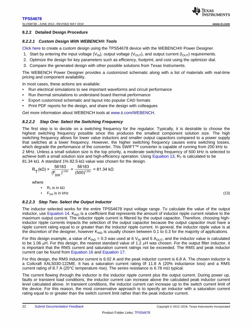
8.2.2.2 Step One: Select the Switching FrequencyThe first step is to decide on a switching frequency for the regulator. Typically, it is desirable to choose thehighest switching frequency possible since this produces the smallest component solution size. The highswitching frequency allows for lower value inductors and smaller output capacitors compared to a power supplythat switches at a lower frequency. However, the higher switching frequency causes extra switching losses,which degrade the performance of the converter. This SWIFT™ converter is capable of running from 200 kHz to2 MHz. Unless a small solution size is the top priority, a moderate switching frequency of 500 kHz is selected toachieve both a small solution size and high-efficiency operation. Using Equation 13, RT is calculated to be81.34 kΩ. A standard 1% 82.5-kΩ value was chosen for the design.
where• RT is in kΩ• FSW is in kHz (13)
8.2.2.3 Step Two: Select the Output InductorThe inductor selected works for the entire TPS54678 input voltage range. To calculate the value of the outputinductor, use Equation 14. KIND is a coefficient that represents the amount of inductor ripple current relative to themaximum output current. The inductor ripple current is filtered by the output capacitor. Therefore, choosing high-inductor ripple currents impacts the selection of the output capacitor because the output capacitor must have aripple current rating equal to or greater than the inductor ripple current. In general, the inductor ripple value is atthe discretion of the designer, however KIND is usually chosen between 0.1 to 0.3 for the majority of applications.
For this design example, a value of KIND = 0.3 was used at 6 VIN and 6 AOUT, and the inductor value is calculatedto be 1.06 μH. For this design, the nearest standard value of 1.2 μH was chosen. For the output filter inductor, itis important that the RMS current and saturation current ratings not be exceeded. The RMS and peak inductorcurrent can be found from Equation 16 and Equation 17.
For this design, the RMS inductor current is 6.02 A and the peak inductor current is 6.8 A. The chosen inductor isa Coilcraft XAL5030-122ME. It has a saturation current rating 0f 11.8 A (20% inductance loss) and a RMScurrent rating of 8.7 A (20°C temperature rise). The series resistance is 6.78 mΩ typical.
The current flowing through the inductor is the inductor ripple current plus the output current. During power up,faults or transient load conditions, the inductor current can increase above the calculated peak inductor currentlevel calculated above. In transient conditions, the inductor current can increase up to the switch current limit ofthe device. For this reason, the most conservative approach is to specify an inductor with a saturation currentrating equal to or greater than the switch current limit rather than the peak inductor current.

( )Bank
5.4 JC 73.17 F
0.7938 0.72
m= = m
-
( )
CAP Initial
CAP Final IND
2 2
22
Energy 0.5 C V 0.5 C 1.2
Energy 0.5 C 1.2 Energy 0.5 C 1.2 0.06
= ´ ´ = ´ ´
= ´ ´ + = ´ ´ +
IND2 2Energy 0.5 L I 0.5 1.2 3 5.4 Joule= ´ ´ = ´ m ´ = m
RIPPLEIND _ peak o
II I
2= +
( )OUT IN_MAX OUT
IND _RMS oIN_MAX SW
2
2V V V1
I I12 V L1 F
æ ö´ -ç ÷= + ´ç ÷´ ´è ø
IN_MAX OUT OUTRIPPLE
IN_MAX SW
V V VI
L1 V F
-
= ´
´
IN_MAX OUT OUT
o IND IN_MAX SW
V V VL1
I K V F
-
= ´
´ ´
23
TPS54678www.ti.com SLVSBF3B –JUNE 2012–REVISED MAY 2019
Product Folder Links: TPS54678
Submit Documentation FeedbackCopyright © 2012–2019, Texas Instruments Incorporated
(14)
(15)
(16)
(17)
8.2.2.4 Step Three: Choose the Output CapacitorThere are three primary considerations for selecting the value of the output capacitor. Along with the inductor, theoutput capacitor determines the output voltage ripple, and also how the regulator responds to a large change inload current. The output capacitance needs to be selected based on the more stringent of these two criteria.
The desired response to a large change in the load current is the first criteria. The output capacitor needs tosupply the load with current when the regulator can not due to limited control speed. The regulator is temporarilynot able to supply sufficient change in output current if there is a large, fast increase or decrease in the currentneeds of the load such as transitioning from no load to full load. The regulator usually needs two or more clockcycles for the control loop to see the change in load current and output voltage and adjust the duty cycle to reactto the change. The output capacitor must be sized to supply the extra current to the load until the control loopresponds to the load change, or conversely, absorb the excess current from the inductor. Because the outputvoltage is less than half the input voltage, the worst-case deviation in output voltage occurs when the load has anextremely rapid reduction in current, or a load dump. The desired specification is a 50% or 3-A load step, and aresulting voltage deviation of no more than 5%, or 60mV. When a load dump occurs, the excess stored current inthe inductor will tend to charge the output capacitors, and the best the converter can achieve to limit the increasein output voltage is to fold back the duty cycle to zero. Under these circumstances, the amount of rise in outputvoltage is defined by the energy from the choke being fully absorbed by the capacitor bank. Equation 18 throughEquation 20 can be used to calculate the required capacitor bank value.
For this example, the transient load response is specified as a 5% change in Vout for a 50% load step from 3 Ato 0 A. So, ΔIOUT = 3 A and ΔVOUT = 0.05 × 1.2 = 0.06 V. Using these numbers gives a minimum capacitance of73.2 μF. This calculation does not take the ESR of the output capacitor into account in the output voltagechange, and it does not account for latency in control loop speed. For ceramic capacitors, the ESR is usuallysmall enough to ignore in this calculation.
(18)
(19)
Solving for C:
(20)
This 73.17 µF defines the minimum capacitance required to meet the transient spec; however, because thecontrol loop speed is finite, more capacitance than this is required to meet desired performance.

OUT _MAXIN
IN SW
I 0.25V
C F
´D =
´
( )IN_MIN OUTOUTRMS OUT
IN_MIN IN_MIN
V VVI I
V V
-= ´ ´
RIPPLEESR
RIPPLE
VR
I<
( )BankRIPPLESW
RIPPLE
1 1C 13.33 F
V8 F
I
= ´ = m´
24
TPS54678SLVSBF3B –JUNE 2012–REVISED MAY 2019 www.ti.com
Product Folder Links: TPS54678
Submit Documentation Feedback Copyright © 2012–2019, Texas Instruments Incorporated
Equation 21 calculates the minimum output capacitance needed to meet the output voltage ripple specification.In this case, the maximum output voltage ripple is 60 mV. Under this requirement, Equation 21 yields 13.33 µF.
where• FSW is the switching frequency,• VRIPPLE is the maximum allowable output voltage ripple,• and Iripple is the inductor ripple current. (21)
Equation 22 calculates the maximum ESR for the capacitor bank to meet the output voltage ripple specification.Equation 22 indicates the ESR should be less than 37.5 mΩ. In this case, the ESR of the ceramic capacitor bankis less than 37.5 mΩ.
(22)
Additional capacitance de-ratings for aging, temperature and DC bias should be factored in which increases theminimum value calculated in Equation 20. For this example, five 47-μF 10-V X5R ceramic capacitors with 3 mΩof ESR are used. The estimated capacitance after derating is 5 × 47 μF × 0.9 = 211.5 μF.
8.2.2.5 Step Four: Select the Input CapacitorThe TPS54678 requires a high-quality ceramic, type X5R or X7R, input-decoupling capacitor of at least 10 μF ofeffective capacitance and in some applications a bulk capacitance. The effective capacitance includes any DCbias effects. The voltage rating of the input capacitor must be greater than the maximum input voltage. Thecapacitor must also have a ripple current rating greater than the maximum input current ripple of the TPS54678.The input ripple current can be calculated using Equation 23.
(23)
The value of a ceramic capacitor varies significantly over temperature and the amount of DC bias applied to thecapacitor. The capacitance variations due to temperature can be minimized by selecting a dielectric material thatis stable over temperature. X5R and X7R ceramic dielectrics are usually selected for power regulator capacitorsbecause they have a high capacitance to volume ratio and are fairly stable over temperature. The outputcapacitor must also be selected with the DC bias taken into account. The capacitance value of a capacitordecreases as the DC bias across a capacitor increases.
For this example design, a ceramic capacitor with at least a 10-V voltage rating is required to support themaximum input voltage. For this example, three 47-μF and one 0.10-μF 10-V capacitors in parallel have beenselected. In addition to these low ESR capacitors, an input bulk cap of 220-µF electrolytic is included so as toprovide low source impedance at low frequencies for instances where the input voltage source is connected witha lossy feed.
The input capacitance value determines the input ripple voltage of the regulator. The input voltage ripple can becalculated using Equation 24. Using the design example values, IOUT_MAX = 6 A, CIN = 141 μF (neglecting theelectrolytic due to high ESR), FSW = 500 kHz, yields an input voltage ripple of 21.3 mV and an rms input ripplecurrent of 2.94 A.
(24)

( ) ( )OUT _MIN ON_MIN SW _MAX IN_MAX OUT _MIN DS(ON)MIN OUT _MIN L DS(ON)MINV t F V I R I R R= ´ - ´ - ´ +
OUT9 10
REF
VR R 1
V
æ ö= ´ -ç ÷
è ø
SS SSC 3 T= ´
25
TPS54678www.ti.com SLVSBF3B –JUNE 2012–REVISED MAY 2019
Product Folder Links: TPS54678
Submit Documentation FeedbackCopyright © 2012–2019, Texas Instruments Incorporated
8.2.2.6 Step Five: Choose the Soft-Start CapacitorThe slow-start capacitor determines the minimum amount of time it takes for the output voltage to reach thenominal programmed value during power up. This is useful if a load requires a controlled voltage slew rate. Thisis also used if the output capacitance is very large and would require large amounts of current to quickly chargethe capacitor to the output voltage level. The large currents necessary to charge the capacitor may cause theTPS54678 to trip OCP, or excessive current draw from the input power supply may cause the input voltage rail tosag. Limiting the output voltage slew rate mitigates both of these issues.
The slow-start capacitor value can be calculated using Equation 25. For the example circuit, the slow-start time isnot critical because the output capacitor value is 5 × 47 μF which does not require much current to charge to1.2 V. The example circuit has the slow-start time set to an arbitrary value of 3.33 ms, which requires a 10-nFcapacitor.
(25)
8.2.2.7 Step Six: Select the Bootstrap CapacitorA 0.1-μF ceramic capacitor must be connected between the BOOT and PH pins for proper operation. TIrecommends to use a ceramic capacitor with X5R or better grade dielectric. The capacitor should have 10 V orhigher voltage rating.
8.2.2.8 Step Eight: Select Output Voltage and Feedback ResistorsFor the example design, 20 kΩ was selected for R10. Using Equation 26, R9 is calculated also as 20 kΩ.
(26)
8.2.2.8.1 Output Voltage Limitations
Due to the internal design of the TPS54678, there is a minimum output voltage limit for any given input voltage.The output voltage can never be lower than the internal voltage reference of 0.6 V. Above 0.6 V, the outputvoltage may be limited by the minimum controllable ON-time. The minimum output voltage in this case is givenby Equation 27.
where• VOUT_MIN = minimum achievable output voltage• tON_MIN = minimum controllable ON-time (100 ns typical, 120 ns no load)• FSW_MAX = maximum switching frequency including tolerance• VIN_MAX = maximum input voltage• IOUT_MIN = minimum load current• RDS(ON)_MIN = minimum high-side MOSFET ON-resistance (see Electrical Characteristics)• RL = series resistance of output inductor (27)

100 1000 10000 100000 1000000−50
−40
−30
−20
−10
0
10
20
30
−225
−180
−135
−90
−45
0
45
90
135
Frequency (Hz)
Gai
n (d
B)
Pha
se (
°)
GainPhase
G001
PMOD
OUT LOAD
1F
2 C R=
p
( ) ( )OFF _MAXOUT _MAX OUT _MAX DS(ON)MAX L OUT _MAX DS(ON)MAX
DEAD
tV V 1 I R R 0.7 I RIN Period
t
Period
æ ö= ´ - - ´ + - - ´ç ÷ç ÷
è ø
æ ö´ ç ÷
è ø
26
TPS54678SLVSBF3B –JUNE 2012–REVISED MAY 2019 www.ti.com
Product Folder Links: TPS54678
Submit Documentation Feedback Copyright © 2012–2019, Texas Instruments Incorporated
There is also a maximum achievable output voltage which is limited by the minimum off time. The maximumoutput voltage is given by Equation 28.
where• VOUT_MAX = maximum achievable output voltage• VIN = minimum input voltage• tOFF_MAX = maximum OFF-time (180 ns typical for adequate margin)• Period = 1/Fs• IOUT_MAX = maximum current• RDS(ON)_MAX = maximum high-side MOSFET ON-resistance (see Electrical Characteristics)• RL = DCR of the inductor• tDEAD = dead time (40 ns) (28)
8.2.2.9 Step Nine: Select Loop Compensation ComponentsThere are several possible methods to design closed-loop compensation for DC/DC converters. For the idealcurrent mode control, the design equations can be easily simplified. The power stage gain is constant at lowfrequencies, and rolls off at –20 dB/decade above the modulator pole frequency. The power stage phase is zerodegrees at low frequencies and starts to fall one decade below the modulator pole frequency reaching aminimum of –90 degrees one decade above the modulator pole frequency. In this case the modulator pole is asimple pole shown in Equation 29.
(29)
For the TPS54678 most circuits will have relatively high amounts of slope compensation. As more slopecompensation is applied, the power stage characteristics will deviate from the ideal approximations. The phaseloss of the power stage will extend beyond –90 degrees and can approach –180 degrees, making compensationmore difficult. The power stage transfer function can be solved but it is a tedious hand calculation that does notlend itself to simple approximations. It is easier to either simulate the circuit or to actually measure the planttransfer function so that a reliable compensation circuit can be designed. The latter technique used in this designprocedure. The power stage plant was measured and is shown in Figure 31.
Figure 31. Measured Plant Bode
For this design, the desired crossover frequency Fc is 50 kHz. From the power stage gain and phase plot above,the gain at 50 kHz is –10.6 dB and the phase is –123.3 degrees. Because the plant phase loss is greater than–90 degrees, to achieve at least 60 degrees of phase margin, additional phase boost from a feedforwardcapacitor in parallel with the upper resistor of the voltage set point divider is required.

15
9 c
O
R
U
F
T
E
1C
V2 R F
V
=
p
( )p15 9 10
1F
2 C R || R=
p
z
15 9
1F
2 C R=
p
53 pole
1C
2 R F=
p
63 plant pole
1C
2 R F=
p
Plant
3EA REF
OUT
G
20V10
Rgm V
-æ öç ÷è ø
= ´
27
TPS54678www.ti.com SLVSBF3B –JUNE 2012–REVISED MAY 2019
Product Folder Links: TPS54678
Submit Documentation FeedbackCopyright © 2012–2019, Texas Instruments Incorporated
See the schematic in Figure 30. R3 sets the gain of the compensated error amplifier to be equal and opposite (indB) to the power stage gain at Fc, so 10.6 dB is needed. The required value of R3 can be calculated fromEquation 30.
(30)
The compensator zero formed by R3 and C6 is placed at the plant pole, as shown approximately 2.5 kHz. Therequired value for C6 is given by Equation 31.
(31)
The high-frequency noise pole formed by C5 and R3 is not used in this design. If the resulting design showsnoise susceptibility, the value of C5 can be calculated per Equation 32.
(32)
To avoid a penalty in loop phase, the Fpole in Equation 32 should be placed a decade above Fc or higher, and isintended to reject noise at FSW.
The feedforward capacitor C15 is used to increase the phase boost at crossover above what is normallyavailable from Type II compensation. It places an additional zero/pole pair with the zero located at Equation 33and the pole at Equation 34.
(33)
(34)
This zero and pole pair is not independent since R9 and R10 are set by the desired VOUT. Once the zero locationis chosen, the pole is fixed as well. For optimum performance, the zero and pole should be located symmetricallyabout the intended crossover frequency. The required value for C15 can be calculated from Equation 35.
(35)
Table 2 lists the values the compensation equations yield.
Table 2. Frequency Compensation Component ValuesREF DES CALCULATED VALUE CHOSEN VALUE
R3 19.6 kΩ 26.7 kΩC6 2.38 nF 2.2 nF
C15 225 pF 150 pF

80
82
84
86
88
90
92
94
96
0 0.5 1 1.5 2 2.5 3 3.5 4 4.5 5 5.5 6Output Current (A)
Effi
cien
cy (
%)
3 V4 V5 V6 V
G002
1.2050
1.2055
1.2060
1.2065
1.2070
1.2075
1.2080
1.2085
1.2090
1.2095
1.2100
0 0.5 1 1.5 2 2.5 3 3.5 4 4.5 5 5.5 6Output Current (A)
Out
put V
olta
ge (
V)
3 V4 V5 V6 V
G003
28
TPS54678SLVSBF3B –JUNE 2012–REVISED MAY 2019 www.ti.com
Product Folder Links: TPS54678
Submit Documentation Feedback Copyright © 2012–2019, Texas Instruments Incorporated
8.2.3 Application CurvesFigure 32 through Figure 47 were measured on the TPS54678 Evaluation Module. More explanation ofwaveforms, as well as a schematic document can be found in the TPS54678EVM-155 6-A, SWIFT™ RegulatorEvaluation Module user guide, SLVU747.
8.2.3.1 Additional Information About Application Curves
8.2.3.1.1 Efficiency
System efficiency may be lower than shown in Figure 32 at higher ambient temperatures, due to temperaturevariation in the drain-to-source resistance RDS(ON) of the internal MOSFETs.
8.2.3.1.2 Voltage Ripple Measurements
Probe placement and noise pickup can give unreliable voltage ripple results. Figure 37 and Figure 38 show theoutput voltage ripple of the converter, measured directly across the output capacitors. Likewise, Figure 39 andFigure 40 show the input voltage ripple of the converter, measured directly across the input capacitors.
8.2.3.1.3 Start-Up and Shutdown Waveforms
Figure 41 and Figure 42 show the start-up waveforms for the TPS54678EVM-155. In Figure 41, the outputvoltage ramps up as soon as the input voltage reaches the UVLO threshold as set by the R1 and R2 resistordivider network. In Figure 42, the input voltage is initially applied and the output is inhibited by using a jumper atJP1 to tie EN to GND. When the jumper is removed, EN is released. When the EN voltage reaches the enable-threshold voltage, the start-up sequence begins and the output voltage ramps up to the externally set value of1.2 V.
The TPS54678 is designed to start up into prebiased outputs. Figure 43 shows the output voltage start-upwaveform when the output is prebiased with 550 mV at no load.
Figure 44 and Figure 45 show the shutdown waveforms for the TPS54678EVM-155. In Figure 44, the outputvoltage ramps down as soon as the input voltage falls below the UVLO stop threshold as set by the R1 and R2resistor divider network. At the point of shutdown, the input voltage rises slightly due to the resistive drop in theinput feed impedance. In Figure 45, the output is inhibited by using a jumper at JP1 to tie EN to GND.
8.2.3.1.4 Hiccup Mode Current Limit
The TPS54678 has hiccup mode current limit. When the peak switch current exceeds the current limit threshold,the device shuts down and restarts. Hiccup mode current limit operation is shown in Figure 46 and Figure 47.Figure 46 shows the hiccup mode current limit with a slight resistive overload. When the peak current limit isexceeded, the output voltage is disabled. Figure 47 shows the operation of the TPS54678 with the outputshorted to ground. The device continuously resets until the fault condition is removed.
Figure 32. Efficiency vs Load Current Figure 33. Load Regulation

V = 20 mV / div (ac coupled)OUT
Time = 500 ns/div
SW Node = 5 V / div
V = 6 V
I = 6 AIN
OUT
V = 50 mV / div
(ac coupled)20 MHZ BW Limited
IN
Time = 500 ns/div
SW Node = 5 V / div
V = 3 V
I = 6 AIN
OUT
V = 20 mV / div (ac coupled)OUT
Time = 500 ns/div
SW Node = 5 V / div
V = 3 V
I = 6 AIN
OUT
100 1000 10000 100000 1000000−20
−10
0
10
20
30
40
50
−60
−30
0
30
60
90
120
150
Frequency (Hz)
Gai
n (d
B)
Pha
se (
°)
GainPhase
G005
1.2050
1.2055
1.2060
1.2065
1.2070
1.2075
1.2080
1.2085
1.2090
1.2095
1.2100
3 3.5 4 4.5 5 5.5 6Input Voltage (V)
Out
put V
olta
ge (
V)
3 A4 A5 A6 A
G003
V = 50 mV / div (ac coupled)OUT
Time = 100 s/divm
I = 1 A / divOUT
Load step = 0 - 3 A
29
TPS54678www.ti.com SLVSBF3B –JUNE 2012–REVISED MAY 2019
Product Folder Links: TPS54678
Submit Documentation FeedbackCopyright © 2012–2019, Texas Instruments Incorporated
Figure 34. Line Regulation Figure 35. Transient Response
Figure 36. Loop ResponseVIN = 3 V, IOUT = 6 A
Figure 37. Output Ripple
VIN = 6 V, IOUT = 6 AFigure 38. Output Ripple
VIN = 3 V, IOUT = 6 AFigure 39. Input Ripple

Time = 100 s/divm
V = falling, 200 mV / divOUT
V = 1 V / div (near 2.7 V)IN
I = 6.6 AOUT
I = 1 A / div (invertey for clarity)OUT
Time = 100 s/divm
V = falling, 200 mV / divOUT
V = 1 V / divIN
V = 5 V
I = 6.6 AIN
OUT
I = 1 A / div (inverted for clarity)OUT
I = 1 A / div
(inverted for clarity)OUT
Time = 500 s/divm
V = 200 mV / divOUT
V = 1 V / divIN
I = 4.6 AOUT
I = 1 A / div
(inverted for clarity)OUT
Time = 500 s/divm
V = 200 mV / divOUT
V = 1 V / divIN
I = 4.6 AOUT
V = 50 mV / div (ac coupled)
20 MHZ BW LimitedIN
Time = 500 ns/div
SW Node = 5 V / div
V = 6 V
I = 6 AIN
OUT
I = 1 A / div (inverted for clarity)OUT
Time = 500 s/divm
V = 200 mV / divOUT
V = 1 V / divIN
I = 4.6 AOUT
30
TPS54678SLVSBF3B –JUNE 2012–REVISED MAY 2019 www.ti.com
Product Folder Links: TPS54678
Submit Documentation Feedback Copyright © 2012–2019, Texas Instruments Incorporated
VIN = 6 V, IOUT = 6 AFigure 40. Input Ripple Figure 41. Start-Up Relative to VIN
Figure 42. Start-Up Relative to EnableFigure 43. Start-Up into Prebias
Figure 44. Shutdown Relative to VIN Figure 45. Shutdown Relative to Enable

Time = 5 ms/div
V = 200 mV / divOUT
V = 1 V / divIN
V = 5 V
I = 9.2 A
IN
OUT
I = 1 A / divOUT
Time = 5 ms/div
V = 100 mV / divOUT
V = 6 V
I = short
IN
OUT
I = 5 A / divOUT
31
TPS54678www.ti.com SLVSBF3B –JUNE 2012–REVISED MAY 2019
Product Folder Links: TPS54678
Submit Documentation FeedbackCopyright © 2012–2019, Texas Instruments Incorporated
Figure 46. Hiccup Mode Current Limit Shutdown Figure 47. Hiccup Mode Current Limit Restart into ShortCircuit

32
TPS54678SLVSBF3B –JUNE 2012–REVISED MAY 2019 www.ti.com
Product Folder Links: TPS54678
Submit Documentation Feedback Copyright © 2012–2019, Texas Instruments Incorporated
9 Power Supply RecommendationsThese devices are designed to operate from an input voltage supply between 2.95 V and 6 V. This supply mustbe well regulated. Proper bypassing of input supplies and internal regulators is also critical for noiseperformance, as is PCB layout and grounding scheme. See the recommendations in the Layout Guidelinessection.
10 Layout
10.1 Layout GuidelinesLayout is a critical portion of good power supply design. There are several signal paths that conduct fastchanging currents or voltages that can interact with stray inductance or parasitic capacitance to generate noiseor degrade the power supplies performance.• Minimize the loop area formed by the bypass capacitor connections and the VIN pins. See Figure 48 for a
PCB layout example.• Tie the GND pins and AGND pin directly to the thermal pad under the TPS54678 device. Connect the thermal
pad to any internal PCB ground planes using multiple vias directly under the device. Additional vias can beused to connect the top-side ground area to the internal planes near the input and output capacitors. Foroperation at full rated load, the top-side ground area along with any additional internal ground planes mustprovide adequate heat dissipating area.
• Place the input bypass capacitor as close as possible to the device.• Route the PH pin to the output inductor. Because the PH connection is the switching node, place the output
inductor close to the PH pins. Minimize the area of the PCB conductor to prevent excessive capacitivecoupling.
• The boot capacitor must also be located close to the device.• The sensitive analog ground connections for the feedback voltage divider, compensation components, soft-
start capacitor and frequency set resistor must be connected to a separate analog ground trace as shown inFigure 48.
• The RT/CLK pin is particularly sensitive to noise so the RT resistor should be located as close as possible tothe device and routed with minimal trace lengths.
• The additional external components can be placed approximately as shown. It is possible to obtainacceptable performance with alternate PCB layouts, however, this layout has been shown to produce goodresults and can be used as a guide.

33
TPS54678www.ti.com SLVSBF3B –JUNE 2012–REVISED MAY 2019
Product Folder Links: TPS54678
Submit Documentation FeedbackCopyright © 2012–2019, Texas Instruments Incorporated
10.2 Layout Example
Figure 48. TPS54678 Layout Example
10.3 Power Dissipation EstimateThe following formulas show how to estimate the IC power dissipation under continuous conduction mode (CCM)operation. The power dissipation of the IC (Ptot) includes conduction loss (Pcon), dead time loss (Pd), switchingloss (Psw), gate drive loss (Pgd) and supply current loss (Pq).
Pcon = IO2 × RDS(on) (temperature dependent)
where• IO is the output current (A)• RDS(on) is the on-resistance of the high-side MOSFET with given temperature (Ω) (36)
Pd = ƒsw × IO × 0.7 × (20 nS + 20 nS)
where• IO is the output current (A)• ƒsw is the switching frequency (Hz) (37)
Psw = 0.5 × VIN × IO × ƒsw× 7 × 10⁻⁹
where• IO is the output current (A)• VIN is the input voltage (V)• ƒsw is the switching frequency (Hz) (38)
Pgd = 2 × VIN × ƒsw× 6 × 10⁻⁹
where• VIN is the input voltage (V)• ƒsw is the switching frequency (Hz) (39)
Pq = VIN × 500 × 10–6
where• VIN is the input voltage (V) (40)

34
TPS54678SLVSBF3B –JUNE 2012–REVISED MAY 2019 www.ti.com
Product Folder Links: TPS54678
Submit Documentation Feedback Copyright © 2012–2019, Texas Instruments Incorporated
Power Dissipation Estimate (continued)So
Ptot = Pcon + Pd + Psw + Pgd + Pq
where• Ptot is the total device power dissipation (W) (41)
For given TA,TJ = TA + Rth × Ptot
where• Ptot is the total device power dissipation (W)• TA is the ambient temperature (°C)• TJ is the junction temperature (°C)• Rth is the thermal resistance of the package (°C/W) (42)
For given TJ max = 150°CTA max = TJ max – Rth × Ptot
where• Ptot is the total device power dissipation (W)• Rth is the thermal resistance of the package (°C/W)• TJ max is maximum junction temperature (°C)• TA max is maximum ambient temperature (°C) (43)
There are additional power losses in the regulator circuit due to the inductor AC and DC losses and traceresistance that impact the overall efficiency of the regulator.

35
TPS54678www.ti.com SLVSBF3B –JUNE 2012–REVISED MAY 2019
Product Folder Links: TPS54678
Submit Documentation FeedbackCopyright © 2012–2019, Texas Instruments Incorporated
11 Device and Documentation Support
11.1 Device Support
11.1.1 Third-Party Products DisclaimerTI'S PUBLICATION OF INFORMATION REGARDING THIRD-PARTY PRODUCTS OR SERVICES DOES NOTCONSTITUTE AN ENDORSEMENT REGARDING THE SUITABILITY OF SUCH PRODUCTS OR SERVICESOR A WARRANTY, REPRESENTATION OR ENDORSEMENT OF SUCH PRODUCTS OR SERVICES, EITHERALONE OR IN COMBINATION WITH ANY TI PRODUCT OR SERVICE.
11.1.2 Development SupportFor more SWIFTTM documentation, see the TI website at www.ti.com/swift.
11.1.2.1 Custom Design With WEBENCH® ToolsClick here to create a custom design using the TPS54678 device with the WEBENCH® Power Designer.1. Start by entering the input voltage (VIN), output voltage (VOUT), and output current (IOUT) requirements.2. Optimize the design for key parameters such as efficiency, footprint, and cost using the optimizer dial.3. Compare the generated design with other possible solutions from Texas Instruments.
The WEBENCH Power Designer provides a customized schematic along with a list of materials with real-timepricing and component availability.
In most cases, these actions are available:• Run electrical simulations to see important waveforms and circuit performance• Run thermal simulations to understand board thermal performance• Export customized schematic and layout into popular CAD formats• Print PDF reports for the design, and share the design with colleagues
Get more information about WEBENCH tools at www.ti.com/WEBENCH.
11.2 Documentation Support
11.2.1 Related DocumentationFor related documentation, see the following:
TPS54678EVM-155 6-A, SWIFT™ Regulator Evaluation Module
11.3 Receiving Notification of Documentation UpdatesTo receive notification of documentation updates, navigate to the device product folder on ti.com. In the upperright corner, click on Alert me to register and receive a weekly digest of any product information that haschanged. For change details, review the revision history included in any revised document.
11.4 Community ResourcesThe following links connect to TI community resources. Linked contents are provided "AS IS" by the respectivecontributors. They do not constitute TI specifications and do not necessarily reflect TI's views; see TI's Terms ofUse.
TI E2E™ Online Community TI's Engineer-to-Engineer (E2E) Community. Created to foster collaborationamong engineers. At e2e.ti.com, you can ask questions, share knowledge, explore ideas and helpsolve problems with fellow engineers.
Design Support TI's Design Support Quickly find helpful E2E forums along with design support tools andcontact information for technical support.

36
TPS54678SLVSBF3B –JUNE 2012–REVISED MAY 2019 www.ti.com
Product Folder Links: TPS54678
Submit Documentation Feedback Copyright © 2012–2019, Texas Instruments Incorporated
11.5 TrademarksSWIFT, E2E are trademarks of Texas Instruments.WEBENCH is a registered trademark of Texas Instruments.All other trademarks are the property of their respective owners.
11.6 Electrostatic Discharge CautionThese devices have limited built-in ESD protection. The leads should be shorted together or the device placed in conductive foamduring storage or handling to prevent electrostatic damage to the MOS gates.
11.7 GlossarySLYZ022 — TI Glossary.
This glossary lists and explains terms, acronyms, and definitions.
12 Mechanical, Packaging, and Orderable InformationThe following pages include mechanical, packaging, and orderable information. This information is the mostcurrent data available for the designated devices. This data is subject to change without notice and revision ofthis document. For browser-based versions of this data sheet, refer to the left-hand navigation.

PACKAGE OPTION ADDENDUM
www.ti.com 10-Dec-2020
Addendum-Page 1
PACKAGING INFORMATION
Orderable Device Status(1)
Package Type PackageDrawing
Pins PackageQty
Eco Plan(2)
Lead finish/Ball material
(6)
MSL Peak Temp(3)
Op Temp (°C) Device Marking(4/5)
Samples
TPS54678RTER ACTIVE WQFN RTE 16 3000 RoHS & Green NIPDAU Level-2-260C-1 YEAR -40 to 150 54678
TPS54678RTET ACTIVE WQFN RTE 16 250 RoHS & Green NIPDAU Level-2-260C-1 YEAR -40 to 150 54678
(1) The marketing status values are defined as follows:ACTIVE: Product device recommended for new designs.LIFEBUY: TI has announced that the device will be discontinued, and a lifetime-buy period is in effect.NRND: Not recommended for new designs. Device is in production to support existing customers, but TI does not recommend using this part in a new design.PREVIEW: Device has been announced but is not in production. Samples may or may not be available.OBSOLETE: TI has discontinued the production of the device.
(2) RoHS: TI defines "RoHS" to mean semiconductor products that are compliant with the current EU RoHS requirements for all 10 RoHS substances, including the requirement that RoHS substancedo not exceed 0.1% by weight in homogeneous materials. Where designed to be soldered at high temperatures, "RoHS" products are suitable for use in specified lead-free processes. TI mayreference these types of products as "Pb-Free".RoHS Exempt: TI defines "RoHS Exempt" to mean products that contain lead but are compliant with EU RoHS pursuant to a specific EU RoHS exemption.Green: TI defines "Green" to mean the content of Chlorine (Cl) and Bromine (Br) based flame retardants meet JS709B low halogen requirements of <=1000ppm threshold. Antimony trioxide basedflame retardants must also meet the <=1000ppm threshold requirement.
(3) MSL, Peak Temp. - The Moisture Sensitivity Level rating according to the JEDEC industry standard classifications, and peak solder temperature.
(4) There may be additional marking, which relates to the logo, the lot trace code information, or the environmental category on the device.
(5) Multiple Device Markings will be inside parentheses. Only one Device Marking contained in parentheses and separated by a "~" will appear on a device. If a line is indented then it is a continuationof the previous line and the two combined represent the entire Device Marking for that device.
(6) Lead finish/Ball material - Orderable Devices may have multiple material finish options. Finish options are separated by a vertical ruled line. Lead finish/Ball material values may wrap to twolines if the finish value exceeds the maximum column width.
Important Information and Disclaimer:The information provided on this page represents TI's knowledge and belief as of the date that it is provided. TI bases its knowledge and belief on informationprovided by third parties, and makes no representation or warranty as to the accuracy of such information. Efforts are underway to better integrate information from third parties. TI has taken andcontinues to take reasonable steps to provide representative and accurate information but may not have conducted destructive testing or chemical analysis on incoming materials and chemicals.TI and TI suppliers consider certain information to be proprietary, and thus CAS numbers and other limited information may not be available for release.
In no event shall TI's liability arising out of such information exceed the total purchase price of the TI part(s) at issue in this document sold by TI to Customer on an annual basis.

PACKAGE OPTION ADDENDUM
www.ti.com 10-Dec-2020
Addendum-Page 2

TAPE AND REEL INFORMATION
*All dimensions are nominal
Device PackageType
PackageDrawing
Pins SPQ ReelDiameter
(mm)
ReelWidth
W1 (mm)
A0(mm)
B0(mm)
K0(mm)
P1(mm)
W(mm)
Pin1Quadrant
TPS54678RTER WQFN RTE 16 3000 330.0 12.4 3.3 3.3 1.1 8.0 12.0 Q2
TPS54678RTET WQFN RTE 16 250 180.0 12.4 3.3 3.3 1.1 8.0 12.0 Q2
PACKAGE MATERIALS INFORMATION
www.ti.com 23-May-2019
Pack Materials-Page 1

*All dimensions are nominal
Device Package Type Package Drawing Pins SPQ Length (mm) Width (mm) Height (mm)
TPS54678RTER WQFN RTE 16 3000 367.0 367.0 35.0
TPS54678RTET WQFN RTE 16 250 210.0 185.0 35.0
PACKAGE MATERIALS INFORMATION
www.ti.com 23-May-2019
Pack Materials-Page 2


IMPORTANT NOTICE AND DISCLAIMER
TI PROVIDES TECHNICAL AND RELIABILITY DATA (INCLUDING DATASHEETS), DESIGN RESOURCES (INCLUDING REFERENCE DESIGNS), APPLICATION OR OTHER DESIGN ADVICE, WEB TOOLS, SAFETY INFORMATION, AND OTHER RESOURCES “AS IS” AND WITH ALL FAULTS, AND DISCLAIMS ALL WARRANTIES, EXPRESS AND IMPLIED, INCLUDING WITHOUT LIMITATION ANY IMPLIED WARRANTIES OF MERCHANTABILITY, FITNESS FOR A PARTICULAR PURPOSE OR NON-INFRINGEMENT OF THIRD PARTY INTELLECTUAL PROPERTY RIGHTS.These resources are intended for skilled developers designing with TI products. You are solely responsible for (1) selecting the appropriate TI products for your application, (2) designing, validating and testing your application, and (3) ensuring your application meets applicable standards, and any other safety, security, or other requirements. These resources are subject to change without notice. TI grants you permission to use these resources only for development of an application that uses the TI products described in the resource. Other reproduction and display of these resources is prohibited. No license is granted to any other TI intellectual property right or to any third party intellectual property right. TI disclaims responsibility for, and you will fully indemnify TI and its representatives against, any claims, damages, costs, losses, and liabilities arising out of your use of these resources.TI’s products are provided subject to TI’s Terms of Sale (www.ti.com/legal/termsofsale.html) or other applicable terms available either on ti.com or provided in conjunction with such TI products. TI’s provision of these resources does not expand or otherwise alter TI’s applicable warranties or warranty disclaimers for TI products.
Mailing Address: Texas Instruments, Post Office Box 655303, Dallas, Texas 75265Copyright © 2020, Texas Instruments Incorporated