tps54719 2.95-v to 6-v input, 7-a synchronous step down
TRANSCRIPT
TPS54719 2.95-V To 6-V Input, 7-A Synchronous Step Down Converter
1 Features• Two 30-mΩ (typical) MOSFETs for high efficiency
at 7-A loads• 200-kHz to 2-MHz switching frequency• 0.6 V ± 1.5% voltage reference over temperature• Adjustable slow start/sequencing• UV and OV power-good output• Low operating and shutdown quiescent current• Safe start-up into pre-biased output• Cycle-by-cycle current limit, thermal and frequency
foldback protection• –40°C to 140°C operating junction temperature
range• Thermally enhanced 3-mm × 3-mm 16-pin QFN
2 Applications• Low-voltage, high-density power systems• Point-of-load regulation for high performance
DSPs, FPGAs, ASICs, and microprocessors• Broadband, networking, and optical
communications infrastructure
3 DescriptionThe TPS54719 device is a full featured 6-V, 7-A, synchronous step down current mode converter with two integrated MOSFETs.
The TPS54719 enables small designs by integrating the MOSFETs, implementing current mode control to
reduce external component count, reducing inductor size by enabling up to 2-MHz switching frequency, and minimizing the IC footprint with a small 3-mm × 3-mm thermally enhanced QFN package.
The TPS54719 provides accurate regulation for a variety of loads with an accurate ±1.5% Voltage Reference (VREF) over temperature.
Efficiency is maximized through the integrated 30-mΩ MOSFETs and 455-μA typical supply current. Using the enable pin, shutdown supply current is reduced to 1 μA by entering a shutdown mode.
Undervoltage lockout is internally set at 2.4 V, but can be increased by programming the threshold with a resistor network on the enable pin. The output voltage start-up ramp is controlled by the slow-start pin. An open-drain power-good signal indicates the output is within 93% to 108% of its nominal voltage.
Frequency foldback and thermal shutdown protects the device during an overcurrent condition.
The TPS54719 is supported in the WEBENCH™
Software Tool at www.ti.com/webench.
Device InformationPART NUMBER PACKAGE(1) BODY SIZE (NOM)
TPS54719 QFN (16) 3.00 mm × 3.00 mm
(1) For all available packages, see the orderable addendum at the end of the datasheet.
PH
VIN
POWERPAD
BOOT
VSENSE
COMP
TPS54719
EN
RT
SS/TR
PWRGD
Css
RT R3
C1
CBOOT
CO
LO
R1
R2
CI
VOUT
VIN
AGND
GND
R4
R5
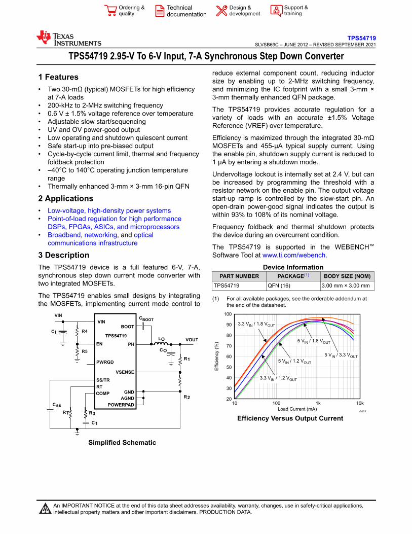
Simplified Schematic
20
30
40
50
60
70
80
90
100
10 100 1k 10k
Load Current (mA)
Effic
iency (
%)
G022
3.3 V / 1.2 VIN OUT
5 V / 1.2 VIN OUT
3.3 V / 1.8 VIN OUT
5 V / 1.8 VIN OUT
5 V / 3.3 VIN OUT
Efficiency Versus Output Current
TPS54719SLVSB69C – JUNE 2012 – REVISED SEPTEMBER 2021
An IMPORTANT NOTICE at the end of this data sheet addresses availability, warranty, changes, use in safety-critical applications, intellectual property matters and other important disclaimers. PRODUCTION DATA.

Table of Contents1 Features............................................................................12 Applications..................................................................... 13 Description.......................................................................14 Revision History.............................................................. 25 Pin Configuration and Functions...................................36 Specifications.................................................................. 4
6.1 Absolute Maximum Ratings........................................ 46.2 ESD Ratings............................................................... 46.3 Recommended Operating Conditions.........................46.4 Thermal Information....................................................56.5 Electrical Characteristics.............................................56.6 Timing Requirements..................................................66.7 Typical Characteristics................................................ 7
7 Detailed Description...................................................... 117.1 Overview................................................................... 117.2 Functional Block Diagram......................................... 127.3 Feature Description...................................................12
7.4 Device Functional Modes..........................................168 Application and Implementation.................................. 21
8.1 Application Information............................................. 218.2 Typical Application.................................................... 21
9 Power Supply Recommendations................................3010 Layout...........................................................................30
10.1 Layout Guidelines................................................... 3010.2 Layout Example...................................................... 31
11 Device and Documentation Support..........................3411.1 Receiving Notification of Documentation Updates.. 3411.2 Support Resources................................................. 3411.3 Trademarks............................................................. 3411.4 Electrostatic Discharge Caution.............................. 3411.5 Glossary.................................................................. 34
12 Mechanical, Packaging, and Orderable Information.................................................................... 34
4 Revision HistoryChanges from Revision B (February 2016) to Revision C (September 2021) Page• Updated the numbering format for tables, figures, and cross-references throughout the document. ................1• Added I/O column to Table 5-1 .......................................................................................................................... 3
Changes from Revision A (July 2014) to Revision B (February 2016) Page• Deleted SWIFT™ from the data sheet title......................................................................................................... 1• Moved Storage temperature to the Section 6.1 ................................................................................................. 4• Changed Handling Ratings to Section 6.2 .........................................................................................................4
TPS54719SLVSB69C – JUNE 2012 – REVISED SEPTEMBER 2021 www.ti.com
2 Submit Document Feedback Copyright © 2021 Texas Instruments Incorporated
Product Folder Links: TPS54719
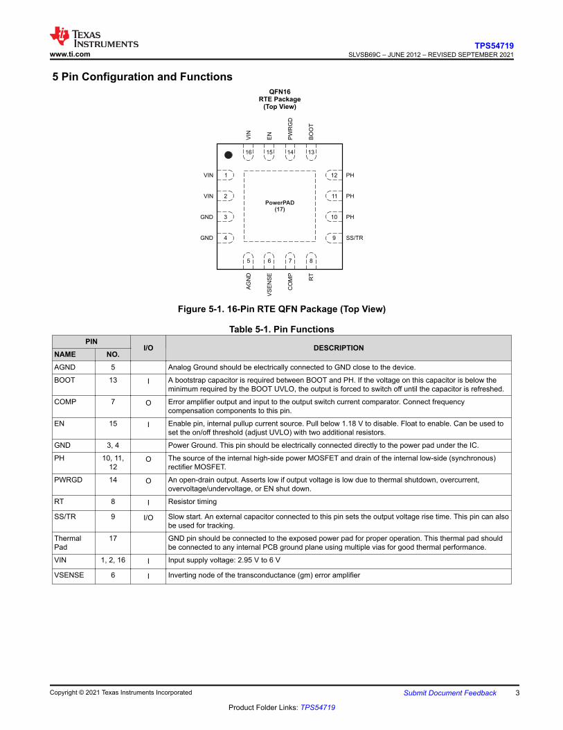
5 Pin Configuration and Functions
PW
RG
D
BO
OT
PH
RT
EN
AG
ND
VIN
VS
EN
SE
CO
MP
15 14 13
GND
12
11
10
9
8765
16
GND
VIN
VIN
PH
PH1
2
3
4 SS/TR
PowerPAD(17)
QFN16RTE Package
(Top View)
Figure 5-1. 16-Pin RTE QFN Package (Top View)
Table 5-1. Pin FunctionsPIN
I/O DESCRIPTIONNAME NO.AGND 5 Analog Ground should be electrically connected to GND close to the device.
BOOT 13 I A bootstrap capacitor is required between BOOT and PH. If the voltage on this capacitor is below the minimum required by the BOOT UVLO, the output is forced to switch off until the capacitor is refreshed.
COMP 7 O Error amplifier output and input to the output switch current comparator. Connect frequency compensation components to this pin.
EN 15 I Enable pin, internal pullup current source. Pull below 1.18 V to disable. Float to enable. Can be used to set the on/off threshold (adjust UVLO) with two additional resistors.
GND 3, 4 Power Ground. This pin should be electrically connected directly to the power pad under the IC.
PH 10, 11, 12
O The source of the internal high-side power MOSFET and drain of the internal low-side (synchronous) rectifier MOSFET.
PWRGD 14 O An open-drain output. Asserts low if output voltage is low due to thermal shutdown, overcurrent, overvoltage/undervoltage, or EN shut down.
RT 8 I Resistor timing
SS/TR 9 I/O Slow start. An external capacitor connected to this pin sets the output voltage rise time. This pin can also be used for tracking.
Thermal Pad
17 GND pin should be connected to the exposed power pad for proper operation. This thermal pad should be connected to any internal PCB ground plane using multiple vias for good thermal performance.
VIN 1, 2, 16 I Input supply voltage: 2.95 V to 6 V
VSENSE 6 I Inverting node of the transconductance (gm) error amplifier
www.ti.comTPS54719
SLVSB69C – JUNE 2012 – REVISED SEPTEMBER 2021
Copyright © 2021 Texas Instruments Incorporated Submit Document Feedback 3
Product Folder Links: TPS54719
6 Specifications6.1 Absolute Maximum Ratingsover operating free-air temperature range (unless otherwise noted) (1)
MIN MAX UNIT
Input voltage
VIN –0.3 7
V
EN –0.3 7
BOOT PH + 8
VSENSE –0.3 3
COMP –0.3 3
PWRGD –0.3 7
SS/TR –0.3 3
RT –0.3 6
Output voltage
BOOT-PH 8
VPH –0.6 7
PH 10 ns Transient –2 7
Source currentEN 100
μART 100
Sink current
COMP 100 μA
PWRGD 10 mA
SS/TR 100 μA
Operating Junction temperature, Tj –40 140 °C
Storage temperature, Tstg –65 150 °C
(1) Stresses beyond those listed under Absolute Maximum Ratings may cause permanent damage to the device. These are stress ratings only, which do not imply functional operation of the device at these or any other conditions beyond those indicated under Recommended Operating Conditions. Exposure to absolute-maximum-rated conditions for extended periods may affect device reliability.
6.2 ESD RatingsVALUE UNIT
V(ESD) Electrostatic dischargeHuman body model (HBM), per ANSI/ESDA/JEDEC JS-001, all pins(1) ±2000
VCharged device model (CDM), per JEDEC specification JESD22-C101, all pins(2)
±500
(1) JEDEC document JEP155 states that 500-V HBM allows safe manufacturing with a standard ESD control process.(2) JEDEC document JEP157 states that 250-V CDM allows safe manufacturing with a standard ESD control process.
6.3 Recommended Operating Conditionsover operating free-air temperature range (unless otherwise noted)
MIN NOM MAX UNITVIN Supply voltage 2.95 6 V
Input voltage
EN 0 6
VPWRGD 0 6
SS/RT 0 2.7
RT 0 5.5
TA Operating free-air temperature –40 85 °C
TPS54719SLVSB69C – JUNE 2012 – REVISED SEPTEMBER 2021 www.ti.com
4 Submit Document Feedback Copyright © 2021 Texas Instruments Incorporated
Product Folder Links: TPS54719
6.4 Thermal Information
THERMAL METRIC (1)TPS54719
UNITSRTE (16 PINS)
RθJA Junction-to-ambient thermal resistance (standard board) 49.1
°C/W
RθJA Junction-to-ambient thermal resistance (custom board)(2) 37.0
ψJT Junction-to-top characterization parameter 0.7
ψJB Junction-to-board characterization parameter 21.8
RθJC(top) Junction-to-case(top) thermal resistance 50.7
RθJC(bot) Junction-to-case(bottom) thermal resistance 7.5
RθJB Junction-to-board thermal resistance 21.8
(1) Power rating at a specific ambient temperature TA should be determined with a junction temperature of 140°C. This is the point where distortion starts to substantially increase. See power dissipation estimate in the application section of this data sheet for more information.
(2) Test boards conditions:a. 2 inches x 2 inches, 4 layers, thickness: 0.062 inchb. 2 oz. copper traces located on the top of the PCBc. 2 oz. copper ground planes on the 2 internal layers and bottom layerd. 4 thermal vias (10mil) located under the device package
6.5 Electrical CharacteristicsTJ = –40°C to 140°C, VIN = 2.95 to 6 V (unless otherwise noted)
DESCRIPTION CONDITIONS MIN TYP MAX UNITSUPPLY VOLTAGE (VIN PIN)Operating input voltage 2.95 6 V
Internal undervoltage lockout threshold Rising VIN 2.4 2.8 V
Internal UVLO hysteresis 0.2 V
Shutdown supply current EN = 0 V, 2.95 V ≤ VIN ≤ 6 V 1 5 μA
Quiescent current – Iq VSENSE = 620 mV, RT = 84 kΩ 455 550 μA
ENABLE AND UVLO (EN PIN)Enable threshold Rising 1.16 1.25 1.37 V
Falling 1.18
Input currentEnable threshold + 50 mV -3.6
μAEnable threshold – 50 mV -0.7
VOLTAGE REFERENCE (VSENSE PIN)
Voltage reference2.95 V ≤ VIN ≤ 6 V, –40°C <TJ < 140°C 0.591 0.600 0.609
V25°C 0.594 0.600 0.606
MOSFET
High-side switch resistanceBOOT-PH = 5 V; TJ = 25°C 26 60
mΩBOOT-PH = 2.95 V; TJ = 25°C 35 70
Low-side switch resistanceVIN = 5 V; TJ = 25°C 26 60
mΩVIN = 2.95 V; TJ = 25°C 35 70
ERROR AMPLIFIERInput current 50 nA
Error amplifier transconductance (gm) –2 μA < I(COMP) < 2 μA, V(COMP) = 1 V 250 μmhos
Error amplifier transconductance (gm) during slow start
–2 μA < I(COMP) < 2 μA, V(COMP) = 0.9 V,Vsense = 0.3 V
85 μmhos
Error amplifier source/sink V(COMP) = 1 V, 100 mV overdrive ±20 μA
COMP to Iswitch gm 25 A/V
www.ti.comTPS54719
SLVSB69C – JUNE 2012 – REVISED SEPTEMBER 2021
Copyright © 2021 Texas Instruments Incorporated Submit Document Feedback 5
Product Folder Links: TPS54719
TJ = –40°C to 140°C, VIN = 2.95 to 6 V (unless otherwise noted)DESCRIPTION CONDITIONS MIN TYP MAX UNIT
CURRENT LIMITCurrent limit threshold 8.5 10.5 A
Low-side reverse current limit –1.5 –2.7 A
THERMAL SHUTDOWNThermalshutdown 150 155 °C
Hysteresis 7.5 °C
TIMING RESISTOR (RT PIN)Switching frequency range using RT mode 200 2000 kHz
Switching frequency RT = 84 kΩ 400 490 600 kHz
BOOT (BOOT PIN)BOOT charge resistance VIN = 5 V 15 Ω
BOOT-PH UVLO VIN = 2.95 V 2.1 2.75 V
SLOW START / TRACKING (SS/TR PIN)Charge current V(SS) = 0.3 V 2.4 μA
SS/TR to VSENSE matching VSSTR = 0.3 V 73 115 mV
SS to reference crossover 98% nominal 0.87 V
SS discharge current (overload) VSENSE = 0 V, VSS = 0.3 V 70 μA
SS discharge voltage (overload) VSENSE = 0 V 80 mV
SS discharge current(UVLO, EN, thermal fault) VIN = 5 V, V(SS) = 0.5 V 1.2 mA
POWER GOOD (PWRGD PIN)
VSENSE thresholdVSENSE rising (Good) 93 % Vref
VSENSE rising (Fault) 110 % Vref
Hysteresis VSENSE falling 2 % Vref
Output high leakage VSENSE = VREF, V(PWRGD) = 5.5 V 100 nA
On resistance VIN = 5 V, TJ = 25°C 78 Ω
Minimum VIN for valid output V(PWRGD) < 0.5 V at 100 μA 0.8 V
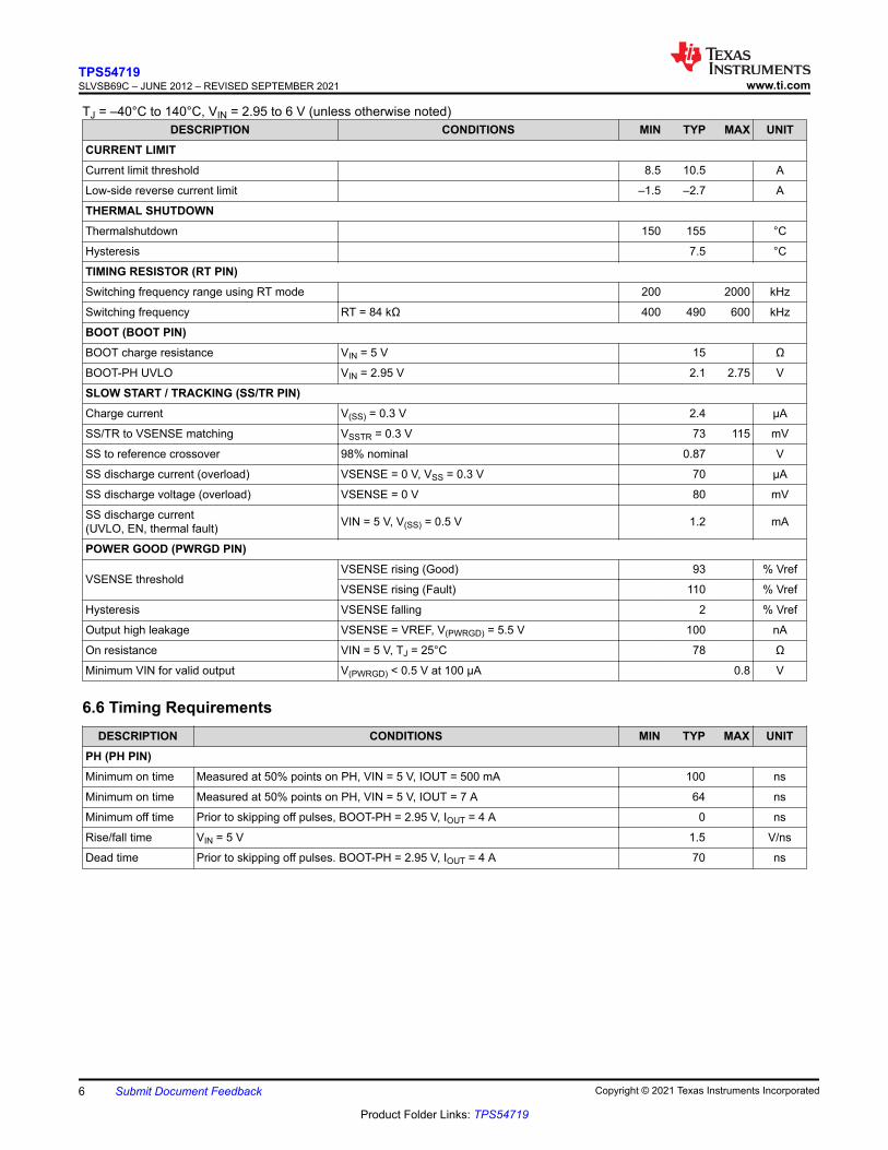
6.6 Timing RequirementsDESCRIPTION CONDITIONS MIN TYP MAX UNIT
PH (PH PIN)Minimum on time Measured at 50% points on PH, VIN = 5 V, IOUT = 500 mA 100 ns
Minimum on time Measured at 50% points on PH, VIN = 5 V, IOUT = 7 A 64 ns
Minimum off time Prior to skipping off pulses, BOOT-PH = 2.95 V, IOUT = 4 A 0 ns
Rise/fall time VIN = 5 V 1.5 V/ns
Dead time Prior to skipping off pulses. BOOT-PH = 2.95 V, IOUT = 4 A 70 ns
TPS54719SLVSB69C – JUNE 2012 – REVISED SEPTEMBER 2021 www.ti.com
6 Submit Document Feedback Copyright © 2021 Texas Instruments Incorporated
Product Folder Links: TPS54719
6.7 Typical Characteristics
0
0.5
1
1.5
2
2.5
−40 −10 20 50 80 110 140
Junction Temperature (°C)
Shutd
ow
n Q
uie
scent C
urr
ent (µ
A) 3.3 Vin
5 Vin
G002
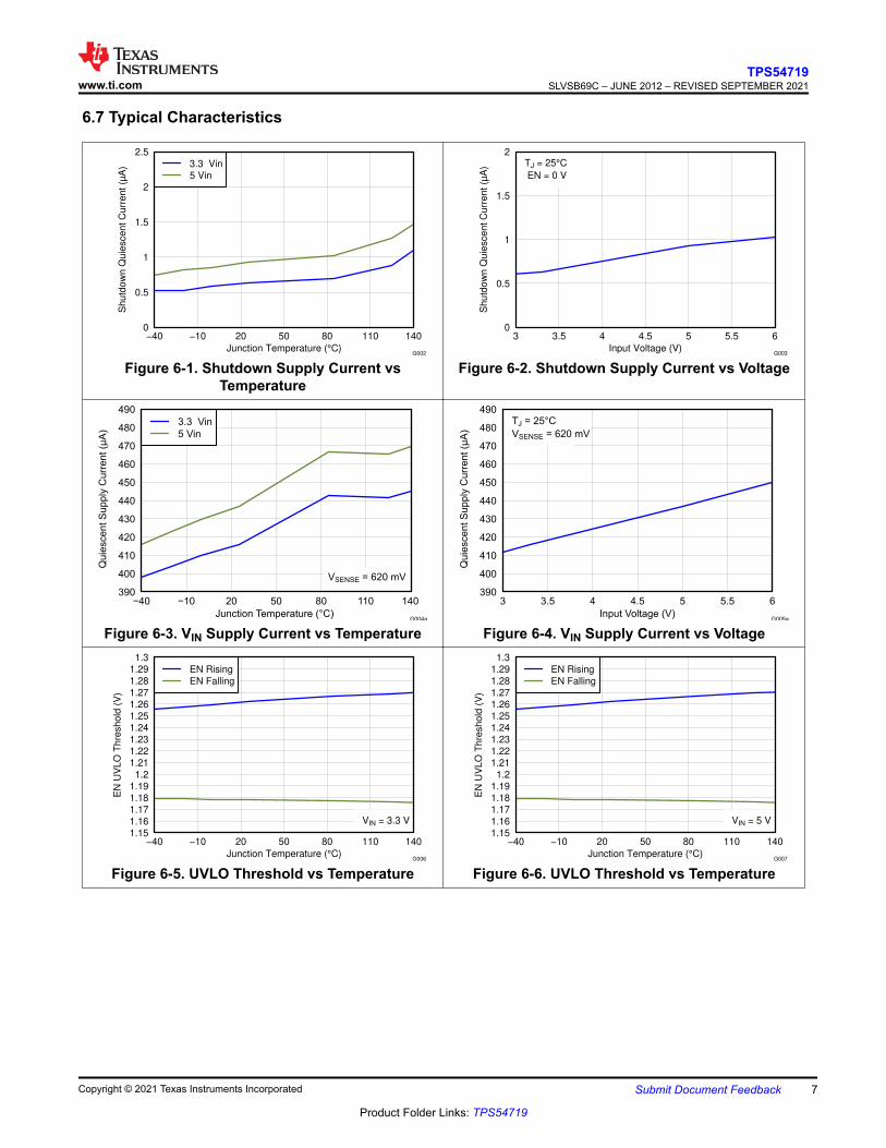
Figure 6-1. Shutdown Supply Current vs Temperature
0
0.5
1
1.5
2
3 3.5 4 4.5 5 5.5 6
Input Voltage (V)
Shutd
ow
n Q
uie
scent C
urr
ent (µ
A) TJ = 25°C
EN = 0 V
G003
Figure 6-2. Shutdown Supply Current vs Voltage
390
400
410
420
430
440
450
460
470
480
490
−40 −10 20 50 80 110 140
Junction Temperature (°C)
Quie
scent S
upply
Curr
ent (µ
A)
3.3 Vin
5 Vin
VSENSE = 620 mV
G004a
Figure 6-3. VIN Supply Current vs Temperature
390
400
410
420
430
440
450
460
470
480
490
3 3.5 4 4.5 5 5.5 6
Input Voltage (V)
Quie
scent S
upply
Curr
ent (µ
A)
TJ = 25°C
VSENSE = 620 mV
G005a
Figure 6-4. VIN Supply Current vs Voltage
1.15
1.161.17
1.18
1.19
1.2
1.211.22
1.23
1.24
1.25
1.261.27
1.28
1.29
1.3
−40 −10 20 50 80 110 140
Junction Temperature (°C)
EN
UV
LO
Thre
shold
(V
)
EN Rising
EN Falling
VIN = 3.3 V
G006
Figure 6-5. UVLO Threshold vs Temperature
1.15
1.161.17
1.18
1.19
1.2
1.211.22
1.23
1.24
1.25
1.261.27
1.28
1.29
1.3
−40 −10 20 50 80 110 140
Junction Temperature (°C)
EN
UV
LO
Thre
shold
(V
)
EN Rising
EN Falling
VIN = 5 V
G007
Figure 6-6. UVLO Threshold vs Temperature
www.ti.comTPS54719
SLVSB69C – JUNE 2012 – REVISED SEPTEMBER 2021
Copyright © 2021 Texas Instruments Incorporated Submit Document Feedback 7
Product Folder Links: TPS54719
−5
−4
−3
−2
−1
0
−40 −10 20 50 80 110 140
Junction Temperature (°C)
EN
Pin
Curr
ent (µ
A)
VEN = Threshold − 50 mVVEN = Threshold + 50 mV
VIN = 3.3 V
G008
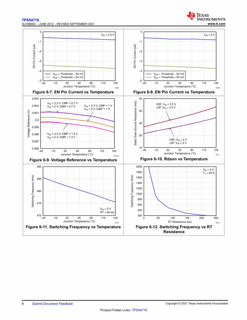
Figure 6-7. EN Pin Current vs Temperature
−5
−4
−3
−2
−1
0
−40 −10 20 50 80 110 140
Junction Temperature (°C)
EN
Pin
Curr
ent (µ
A)
VEN = Threshold − 50 mVVEN = Threshold + 50 mV
VIN = 5 V
G009
Figure 6-8. EN Pin Current vs Temperature
0.596
0.597
0.598
0.599
0.6
0.601
0.602
0.603
−40 −10 20 50 80 110 140
VIN = 3.3 V, CMP = 0.7 V
VIN = 5 V, CMP = 0.7 V VIN = 3.3 V, CMP = 1 V
VIN = 5 V, CMP = 1 V
VIN = 3.3 V, CMP = 1.3 V
VIN = 5 V, CMP = 1.3 V
Junction Temperature (°C)
Voltage R
efe
rence (
V)
G010 a
Figure 6-9. Voltage Reference vs Temperature
10
20
30
40
50
−40 −10 20 50 80 110 140
HSF, VIN = 3.3 V
LSF, VIN = 3.3 V
HSF, VIN = 5 V
LSF, VIN = 5 V
Junction Temperature (°C)
Sta
tic D
rain
Sourc
e R
esis
tance (
mΩ
)
G011
Figure 6-10. Rdson vs Temperature
470
475
480
485
490
−40 −10 20 50 80 110 140
Junction Temperature (°C)
Sw
itchin
g F
requency (
kH
z)
VIN = 5 V
RT = 84 kΩ
G012
Figure 6-11. Switching Frequency vs Temperature
200
400
600
800
1000
1200
1400
1600
1800
2000
0 50 100 150 200 250
RT Resistance (kΩ)
Sw
itchin
g F
requency (
kH
z)
VIN = 5 V
TJ = 25°C
G013
Figure 6-12. Switching Frequency vs RT Resistance
TPS54719SLVSB69C – JUNE 2012 – REVISED SEPTEMBER 2021 www.ti.com
8 Submit Document Feedback Copyright © 2021 Texas Instruments Incorporated
Product Folder Links: TPS54719

0
25
50
75
100
0 0.1 0.2 0.3 0.4 0.5 0.6
VSENSE (V)
Norm
inal S
witchin
g F
requency (
%)
Vsense Rising
Vsense Falling
TJ = 25°C
G014
Figure 6-13. Switching Frequency vs Vsense
−2.45
−2.4
−2.35
−2.3
−2.25
−40 −10 20 50 80 110 140
Junction Temperature (°C)
Charg
e C
urr
ent (µ
A)
VIN = 3.3 VVIN = 5 V
G015
Figure 6-14. SS Charge Current vs Temperature
170
190
210
230
250
270
290
−40 −10 20 50 80 110 140
Junction Temperature (°C)
Tra
nsconducta
nce (
µA
/V)
VIN = 3.3 VVIN = 5 V
G016
Figure 6-15. Transconductance vs Temperature
55
60
65
70
75
80
85
90
95
100
105
−40 −10 20 50 80 110 140
Junction Temperature (°C)
Tra
nsconducta
nce (
µA
/V)
VIN = 3.3 VVIN = 5 V
SS = 0.3 V
G017
Figure 6-16. Transconductance (Slow Start) vs Temperature
8
9
10
11
12
13
−40 −10 20 50 80 110 140
Junction Temperature (°C)
Hig
h S
ide C
urr
ent Lim
it T
hre
shold
(A
) VIN = 5 V
VIN = 3.3 V
G018
Figure 6-17. High-Side FET Current Limit vs Temperature
2
2.5
3
3.5
4
−40 −10 20 50 80 110 140
Junction Temperature (°C)
Low
Sid
e C
urr
ent Lim
itT
hre
shold
(A
)
VIN = 3.3 VVIN = 5 V
G019 a
Figure 6-18. Low-Side FET Current Limit vs Temperature
www.ti.comTPS54719
SLVSB69C – JUNE 2012 – REVISED SEPTEMBER 2021
Copyright © 2021 Texas Instruments Incorporated Submit Document Feedback 9
Product Folder Links: TPS54719
20
30
40
50
60
70
80
90
100
110
120
130
−40 −10 20 50 80 110 140
Junction Temperature (°C)
RdsonP
ow
er
Good (
Ω)
VIN = 5 V
G020
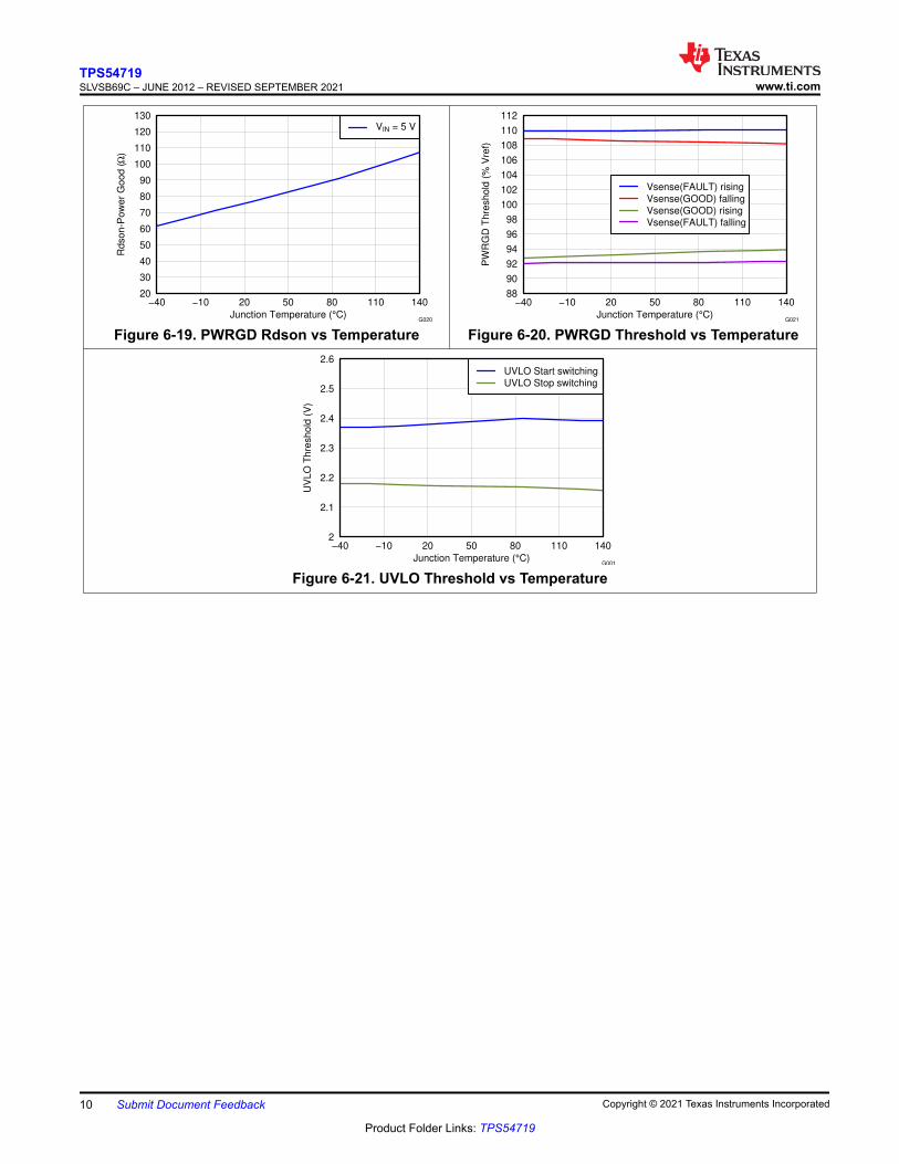
Figure 6-19. PWRGD Rdson vs Temperature
88
90
92
94
96
98
100
102
104
106
108
110
112
−40 −10 20 50 80 110 140
Junction Temperature (°C)
PW
RG
D T
hre
shold
(%
Vre
f)
Vsense(FAULT) rising
Vsense(GOOD) falling
Vsense(GOOD) rising
Vsense(FAULT) falling
G021
Figure 6-20. PWRGD Threshold vs Temperature
2
2.1
2.2
2.3
2.4
2.5
2.6
−40 −10 20 50 80 110 140
Junction Temperature (°C)
UV
LO
Thre
shold
(V
)
UVLO Start switching
UVLO Stop switching
G001
Figure 6-21. UVLO Threshold vs Temperature
TPS54719SLVSB69C – JUNE 2012 – REVISED SEPTEMBER 2021 www.ti.com
10 Submit Document Feedback Copyright © 2021 Texas Instruments Incorporated
Product Folder Links: TPS54719
7 Detailed Description7.1 OverviewThe TPS54719 is a 6-V, 7-A, synchronous step-down (buck) converter with two integrated n-channel MOSFETs. To improve performance during line and load transients, the device implements a constant frequency, peak current mode control, which reduces output capacitance and simplifies external frequency compensation design. The wide switching frequency of 200 kHz to 2000 kHz allows for efficiency and size optimization when selecting the output filter components. The switching frequency is adjusted using a resistor to ground on the RT pin.
The TPS54719 has a typical default start-up voltage of 2.4 V. The EN pin has an internal pullup current source that can be used to adjust the input voltage undervoltage lockout (UVLO) with two external resistors. In addition, the pullup current provides a default condition when the EN pin is floating for the device to operate. The total operating current for the TPS54719 is 455 μA when not switching and under no load. When the device is disabled, the supply current is less than 5 μA.
The integrated 30-mΩ MOSFETs allow for high efficiency power supply designs with continuous output currents up to 7 amperes.
The TPS54719 reduces the external component count by integrating the boot recharge diode. The bias voltage for the integrated high-side MOSFET is supplied by a capacitor on the BOOT to PH pin. The boot capacitor voltage is monitored by an UVLO circuit and turns off the high-side MOSFET when the voltage falls below a preset threshold. This BOOT circuit allows the TPS54719 to operate approaching 100%. The output voltage can be stepped down to as low as the 0.6-V reference.
The TPS54719 has a power-good comparator (PWRGD) with 2% hysteresis.
The TPS54719 minimizes excessive output overvoltage transients by taking advantage of the overvoltage power-good comparator. When the regulated output voltage is greater than 110% of the nominal voltage, the overvoltage comparator is activated, and the high-side MOSFET is turned off and masked from turning on until the output voltage is lower than 108%.
The SS/TR pin is used to minimize inrush currents or provide power supply sequencing during power up. A small value capacitor should be coupled to the pin for slow start. The SS/TR pin is discharged before the output power up to make sure there is a repeatable restart after an over-temperature fault, UVLO fault, or disabled condition.
The use of a frequency foldback circuit reduces the switching frequency during start-up and overcurrent fault conditions to help limit the inductor current.
www.ti.comTPS54719
SLVSB69C – JUNE 2012 – REVISED SEPTEMBER 2021
Copyright © 2021 Texas Instruments Incorporated Submit Document Feedback 11
Product Folder Links: TPS54719

7.2 Functional Block Diagram
ERROR
AMPLIFIER
Boot
Charge
Boot
UVLO
UVLO
Current
Sense
Oscillator
Frequency
Shift
Slope
Compensation
PWM
Comparator
Minimum
COMP Clamp
Maximum
Clamp
Voltage
Reference
Overload
Recovery
VSENSE
SS/TR
COMP
RT
PH
BOOT
VIN
AGND
Thermal
Shutdown
EN
Enable
Comparator
Shutdown
Logic
Shutdown
Enable
Threshold
Logic
Shutdown
PWRGD
THERMALPAD
GND
Logic
Shutdown
107%
93%
S
Logic and PWMLatch
i1 ihys
7.3 Feature Description7.3.1 Fixed Frequency PWM Control
The TPS54719 uses an adjustable fixed frequency, peak current mode control. The output voltage is compared through external resistors on the VSENSE pin to an internal voltage reference by an error amplifier, which drives the COMP pin. An internal oscillator initiates the turn on of the high-side power switch. The error amplifier output is compared to the high-side power switch current. When the power switch current reaches the COMP voltage level, the high-side power switch is turned off and the low-side power switch is turned on. The COMP pin voltage increases and decreases as the output current increases and decreases. The device implements a current limit by clamping the COMP pin voltage to a maximum level and also implements a minimum clamp for improved transient response performance.
7.3.2 Slope Compensation And Output Current
The TPS54719 adds a compensating ramp to the switch current signal. This slope compensation prevents subharmonic oscillations as duty cycle increases. The available peak inductor current remains constant over the full duty cycle range.
TPS54719SLVSB69C – JUNE 2012 – REVISED SEPTEMBER 2021 www.ti.com
12 Submit Document Feedback Copyright © 2021 Texas Instruments Incorporated
Product Folder Links: TPS54719
7.3.3 Bootstrap Voltage (Boot) And Low Dropout Operation
The TPS54719 has an integrated boot regulator and requires a small ceramic capacitor between the BOOT and PH pin to provide the gate drive voltage for the high-side MOSFET. The value of the ceramic capacitor should be 0.1 μF. A ceramic capacitor with an X7R or X5R grade dielectric with a voltage rating of 10 V or higher is recommended because of the stable characteristics over temperature and voltage.
To improve dropout, the TPS54719 is designed to operate at 100% duty cycle as long as the BOOT to PH pin voltage is greater than 2.1 V, typically. The high-side MOSFET is turned off using an UVLO circuit, allowing for the low-side MOSFET to conduct when the voltage from BOOT to PH drops below 2.1 V. Since the supply current sourced from the BOOT pin is very low, the high-side MOSFET can remain on for more switching cycles than are required to refresh the capacitor, thus the effective duty cycle of the switching regulator is very high.
7.3.4 Error Amplifier
The TPS54719 has a transconductance amplifier. The error amplifier compares the VSENSE voltage to the lower of the SS/TR pin voltage or the internal 0.6-V voltage reference. The transconductance of the error amplifier is 250 μA/V during normal operation. When the voltage of VSENSE pin is below 0.6 V and the device is regulating using the SS/TR voltage, the gm is 85 μA/V. The frequency compensation components are placed between the COMP pin and ground.
7.3.5 Voltage Reference
The voltage reference system produces a precise ±1.5% voltage reference over temperature by scaling the output of a temperature stable bandgap circuit. The bandgap and scaling circuits produce 0.6 V at the non-inverting input of the error amplifier.
7.3.6 Adjusting The Output Voltage
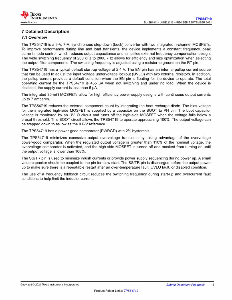
The output voltage is set with a resistor divider from the output node to the VSENSE pin. It is recommended to use divider resistors with 1% tolerance or better. Start with a 100 kΩ for the R1 resistor and use the Equation 1 to calculate R2. To improve efficiency at very light loads consider using larger value resistors. If the values are too high the regulator is more susceptible to noise and voltage errors from the VSENSE input current are noticeable.
æ ö´ ç ÷
-è øO
0.6 VR2 = R1
V 0.6 V (1)
VSENSE
VO
+
-
TPS54719
R1
R20.6 V
Figure 7-1. Voltage Divider Circuit
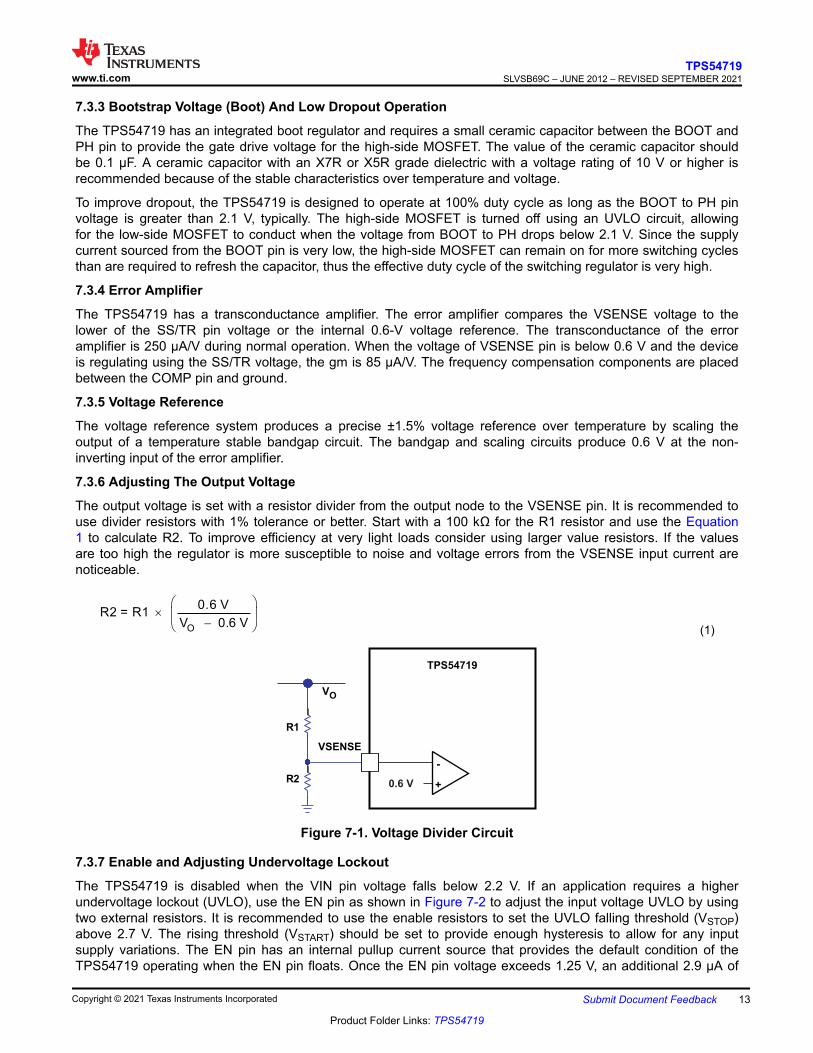
7.3.7 Enable and Adjusting Undervoltage Lockout
The TPS54719 is disabled when the VIN pin voltage falls below 2.2 V. If an application requires a higher undervoltage lockout (UVLO), use the EN pin as shown in Figure 7-2 to adjust the input voltage UVLO by using two external resistors. It is recommended to use the enable resistors to set the UVLO falling threshold (VSTOP) above 2.7 V. The rising threshold (VSTART) should be set to provide enough hysteresis to allow for any input supply variations. The EN pin has an internal pullup current source that provides the default condition of the TPS54719 operating when the EN pin floats. Once the EN pin voltage exceeds 1.25 V, an additional 2.9 μA of
www.ti.comTPS54719
SLVSB69C – JUNE 2012 – REVISED SEPTEMBER 2021
Copyright © 2021 Texas Instruments Incorporated Submit Document Feedback 13
Product Folder Links: TPS54719
hysteresis is added. When the EN pin is pulled below 1.18 V, the 2.9 μA is removed. This additional current facilitates input voltage hysteresis.
0.7 mA
EN
i1
ihysVIN
+
-
TPS54719
R1
R2
2.9 mA
Figure 7-2. Adjustable Undervoltage Lockout
æ ö-ç ÷
è ø
æ ö- +ç ÷
è ø
ENFALLINGSTART STOP
ENRISING
ENFALLINGP h
ENRISING
VV V
VR1 =
VI 1 I
V (2)
( )ENFALLING
STOP ENFALLING P h
R1 VR2 =
V V R1 I I
´
- + + (3)
spacer
where:
• Ih = 2.9 µA• IP = 0.7 µA• VENRISING = 1.25 V• VENFALLING = 1.18 V
7.3.8 Slow Start/Tracking Pin
The TPS54719 regulates to the lower of the SS/TR pin and the internal reference voltage. A capacitor on the SS/TR pin to ground implements a slow start time. The TPS54719 has an internal pullup current source of 2.4 μA, which charges the external slow-start capacitor. Equation 4 calculates the required slow-start capacitor value.
Tss(mS) Iss( A)Css(nF) =
Vref(V)
´ m
(4)
where:
• Tss is the desired slow-start time in ms• Iss is the internal slow start charging current of 2.4 μA• Vref is the internal voltage reference of 0.6 V
If during normal operation, VIN goes below the UVLO, the EN pin pulled below 1.18 V, or a thermal shutdown event occurs, the TPS54719 stops switching and the SS/TR is discharged to 0 volts before reinitiating a power-up sequence.
TPS54719SLVSB69C – JUNE 2012 – REVISED SEPTEMBER 2021 www.ti.com
14 Submit Document Feedback Copyright © 2021 Texas Instruments Incorporated
Product Folder Links: TPS54719

7.3.9 Sequencing
Many of the common power supply sequencing methods can be implemented using the SS/TR, EN, and PWRGD pins. The sequential method can be implemented using an open-drain or collector output of a power on reset pin of another device. Figure 7-3 shows the sequential method. The power good is coupled to the EN pin on the TPS54719, which enables the second power supply once the primary supply reaches regulation.
Ratio-metric start-up can be accomplished by connecting the SS/TR pins together. The regulator outputs ramp up and reach regulation at the same time. When calculating the slow start time, the pullup current source must be doubled in Equation 4. The ratio metric method is illustrated in Figure 7-5.
SS/TR2
TPS54719
EN2
PWRGD2
SS/TR1
EN1PWRGD1
TPS54719
Figure 7-3. Sequential Start-Up SequenceVout2
Vou t1
PWRGD1
EN2
EN1
Figure 7-4. Sequential Start-Up Using EN And PWRGD
SS/TR1
TPS54719
EN1
PWRGD1
SS/TR2
TPS54719
EN2
PWRGD2
Figure 7-5. Schematic For Ratio-Metric Start-Up Sequence
SS1
Vout2
EN1/2
Vou t1
Figure 7-6. Ratio-Metric Start-Up With VOUT1 Leading VOUT2
Ratio-metric and simultaneous power supply sequencing can be implemented by connecting the resistor network of R1 and R2 shown in Figure 7-5 to the output of the power supply that needs to be tracked or another voltage reference source. Using Equation 5 and Equation 6, the tracking resistors can be calculated to initiate the VOUT2 slightly before, after, or at the same time as VOUT1. Equation 7 is the voltage difference between VOUT1 and VOUT2. The ΔV variable is zero volts for simultaneous sequencing. To minimize the effect of the inherent SS/TR to VSENSE offset (Vssoffset) in the slow start circuit and the offset created by the pullup current source (Iss)
www.ti.comTPS54719
SLVSB69C – JUNE 2012 – REVISED SEPTEMBER 2021
Copyright © 2021 Texas Instruments Incorporated Submit Document Feedback 15
Product Folder Links: TPS54719
and tracking resistors, the Vssoffset and Iss are included as variables in the equations. To design a ratio-metric start-up in which the VOUT2 voltage is slightly greater than the VOUT1 voltage when VOUT2 reaches regulation, use a negative number in Equation 5 through Equation 7 for ΔV. Equation 7 will result in a positive number for applications where the VOUT2 is slightly lower than VOUT1 when VOUT2 regulation is achieved. As the SS/TR voltage becomes more than 85% of the nominal reference voltage, the Vssoffset becomes larger as the slow start circuits gradually handoff the regulation reference to the internal voltage reference. The SS/TR pin voltage needs to be greater than 0.87 V for a complete handoff to the internal voltage reference as shown in Figure 7-6.
D´
Vout2 + V VssoffsetR1 =
Vref Iss (5)
´
D -
Vref R1R2 =
Vout2 + V Vref (6)
V = Vout1 Vout2D - (7)
where:
• VOUT2 is the regulated output of IC2• VOUT1 is the output of IC1 at the moment IC2 just reaches its regulation
SS/TR1
TPS54719
EN1
PWRGD1
SS/TR2
TPS54719
EN2
PWRGD2
VOUT1
VOUT 2
R1
R2
Figure 7-7. Schematic For Ratio-Metric Start-Up Sequence
EN1
Vout2
SS2
Vout1
Figure 7-8. Ratio-Metric Start-Up Using Coupled SS/TR Pins
7.4 Device Functional Modes7.4.1 Constant Switching Frequency And Timing Resistor (RT Pin)
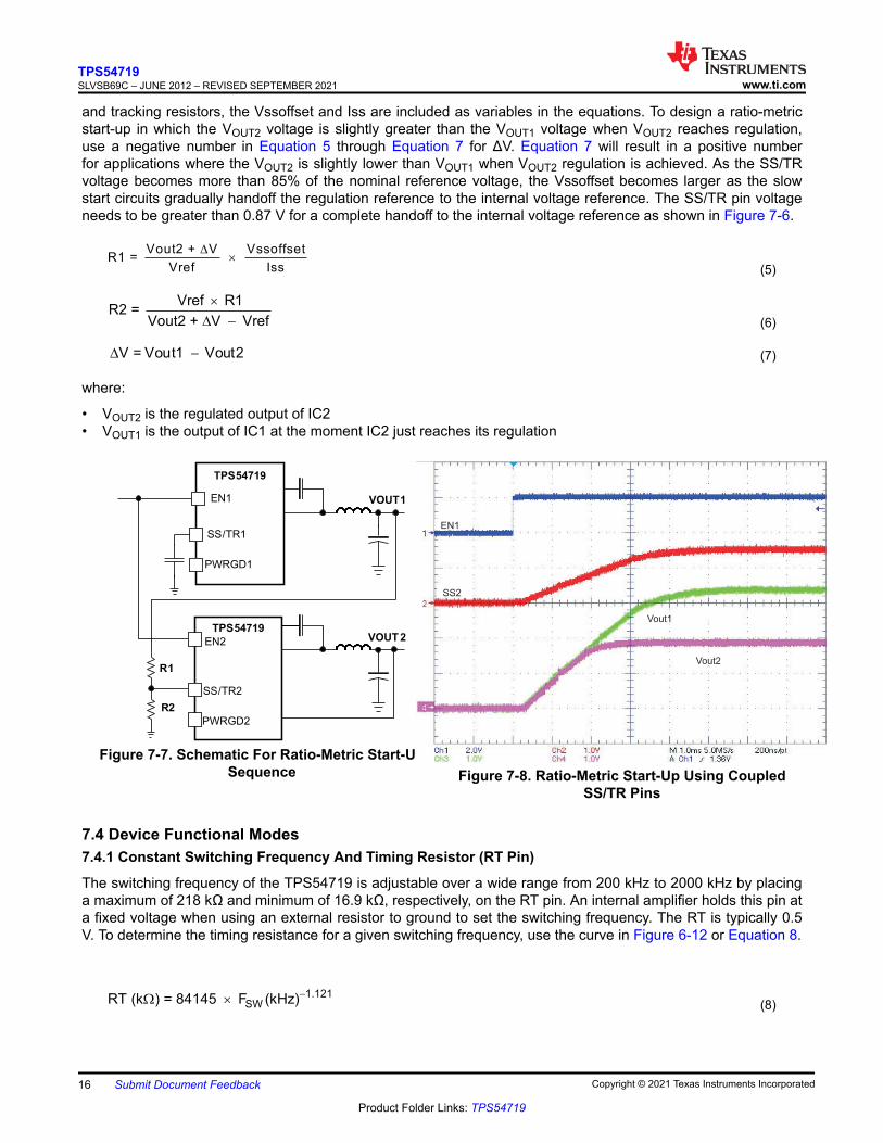
The switching frequency of the TPS54719 is adjustable over a wide range from 200 kHz to 2000 kHz by placing a maximum of 218 kΩ and minimum of 16.9 kΩ, respectively, on the RT pin. An internal amplifier holds this pin at a fixed voltage when using an external resistor to ground to set the switching frequency. The RT is typically 0.5 V. To determine the timing resistance for a given switching frequency, use the curve in Figure 6-12 or Equation 8.
spacer
1.121SWRT (k ) = 84145 F (kHz)-
W ´ (8)
spacer
TPS54719SLVSB69C – JUNE 2012 – REVISED SEPTEMBER 2021 www.ti.com
16 Submit Document Feedback Copyright © 2021 Texas Instruments Incorporated
Product Folder Links: TPS54719

0.89Fsw(kHz) 24517 RT(k )-= ´ W (9)
To reduce the solution size, one would typically set the switching frequency as high as possible, but tradeoffs of the efficiency, maximum input voltage, and minimum controllable on time should be considered.
The minimum controllable on time is typically 64 ns at full current load and 100 ns at no load, and limits the maximum operating input voltage or output voltage.
7.4.2 Overcurrent Protection
The TPS54719 implements a cycle-by-cycle current limit. During each switching cycle, the high-side switch current is compared to the voltage on the COMP pin. When the instantaneous switch current intersects the COMP voltage, the high-side switch is turned off. During overcurrent conditions that pull the output voltage low, the error amplifier responds by driving the COMP pin high, increasing the switch current. The error amplifier output is clamped internally. This clamp functions as a switch current limit.
7.4.3 Frequency Shift
To operate at high switching frequencies and provide protection during overcurrent conditions, the TPS54719 implements a frequency shift. If frequency shift was not implemented, during an overcurrent condition, the low-side MOSFET may not be turned off long enough to reduce the current in the inductor, causing a current runaway. With frequency shift, during an overcurrent condition, the switching frequency is reduced from 100%, then 50%, then 25% as the voltage decreases from 0.6 to 0 volts on VSENSE pin to allow the low-side MOSFET to be off long enough to decrease the current in the inductor. During start-up, the switching frequency increases as the voltage on VSENSE increases from 0 to 0.6 volts. See Figure 6-13 for details.
7.4.4 Reverse Overcurrent Protection
The TPS54719 implements low-side current protection by detecting the voltage across the low-side MOSFET. When the converter sinks current through its low-side FET, the control circuit turns off the low-side MOSFET if the reverse current is more than 2.7 A. By implementing this additional protection scheme, the converter is able to protect itself from excessive current during power cycling and start-up into pre-biased outputs.
7.4.5 Power Good (PWRGD Pin)
The PWRGD pin output is an open-drain MOSFET. The output is pulled low when the VSENSE voltage enters the fault condition by falling below 91% or rising above 110% of the nominal internal reference voltage. There is a 2% hysteresis on the threshold voltage, so when the VSENSE voltage rises to the good condition above 93% or falls below 108% of the internal voltage reference the PWRGD output MOSFET is turned off. It is recommended to use a pullup resistor between the values of 1 kΩ and 100 kΩ to a voltage source that is 6 V or less. The PWRGD is in a valid state once the VIN input voltage is greater than 0.8 V, typically.
7.4.6 Overvoltage Transient Protection
The TPS54719 incorporates an overvoltage transient protection (OVTP) circuit to minimize voltage overshoot when recovering from output fault conditions or strong unload transients. The OVTP feature minimizes the output overshoot by implementing a circuit to compare the VSENSE pin voltage to the OVTP threshold, which is 110% of the internal voltage reference. If the VSENSE pin voltage is greater than the OVTP threshold, the high-side MOSFET is disabled, preventing current from flowing to the output and minimizing output overshoot. When the VSENSE voltage drops lower than the OVTP threshold, which is 108% of the internal voltage reference, the high-side MOSFET is allowed to turn on the next clock cycle.
7.4.7 Thermal Shutdown
The device implements an internal thermal shutdown to protect itself if the junction temperature exceeds 155°C. The thermal shutdown forces the device to stop switching when the junction temperature exceeds the thermal trip threshold. Once the die temperature decreases below 147.5°C, the device reinitiates the power-up sequence by discharging the SS/TR pin to 0 volts. The thermal shutdown hysteresis is 7.5°C.
www.ti.comTPS54719
SLVSB69C – JUNE 2012 – REVISED SEPTEMBER 2021
Copyright © 2021 Texas Instruments Incorporated Submit Document Feedback 17
Product Folder Links: TPS54719
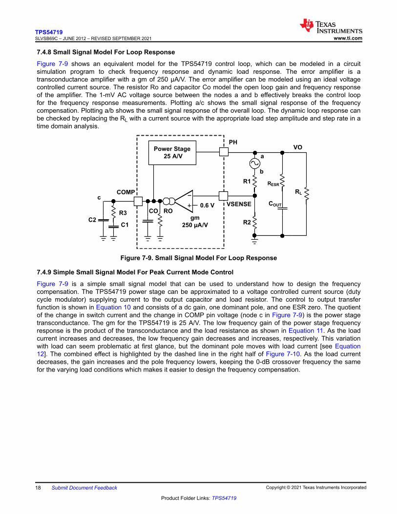
7.4.8 Small Signal Model For Loop Response
Figure 7-9 shows an equivalent model for the TPS54719 control loop, which can be modeled in a circuit simulation program to check frequency response and dynamic load response. The error amplifier is a transconductance amplifier with a gm of 250 μA/V. The error amplifier can be modeled using an ideal voltage controlled current source. The resistor Ro and capacitor Co model the open loop gain and frequency response of the amplifier. The 1-mV AC voltage source between the nodes a and b effectively breaks the control loop for the frequency response measurements. Plotting a/c shows the small signal response of the frequency compensation. Plotting a/b shows the small signal response of the overall loop. The dynamic loop response can be checked by replacing the RL with a current source with the appropriate load step amplitude and step rate in a time domain analysis.
VSENSE
COMP
VO
R1
R3
C1C2 R2
CO ROgm
250 µA/V
Power Stage
25 A/V
PH
RESR
COUT
RL
b
a
c
0.6 V
Figure 7-9. Small Signal Model For Loop Response
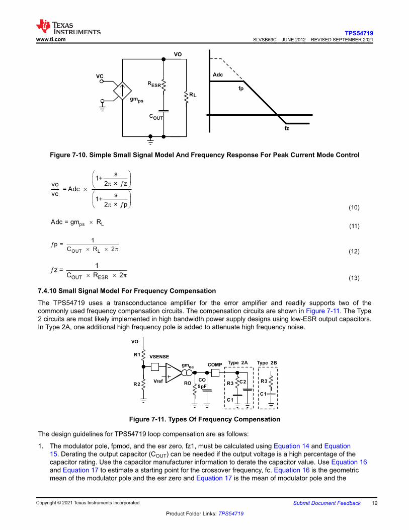
7.4.9 Simple Small Signal Model For Peak Current Mode Control
Figure 7-9 is a simple small signal model that can be used to understand how to design the frequency compensation. The TPS54719 power stage can be approximated to a voltage controlled current source (duty cycle modulator) supplying current to the output capacitor and load resistor. The control to output transfer function is shown in Equation 10 and consists of a dc gain, one dominant pole, and one ESR zero. The quotient of the change in switch current and the change in COMP pin voltage (node c in Figure 7-9) is the power stage transconductance. The gm for the TPS54719 is 25 A/V. The low frequency gain of the power stage frequency response is the product of the transconductance and the load resistance as shown in Equation 11. As the load current increases and decreases, the low frequency gain decreases and increases, respectively. This variation with load can seem problematic at first glance, but the dominant pole moves with load current [see Equation 12]. The combined effect is highlighted by the dashed line in the right half of Figure 7-10. As the load current decreases, the gain increases and the pole frequency lowers, keeping the 0-dB crossover frequency the same for the varying load conditions which makes it easier to design the frequency compensation.
TPS54719SLVSB69C – JUNE 2012 – REVISED SEPTEMBER 2021 www.ti.com
18 Submit Document Feedback Copyright © 2021 Texas Instruments Incorporated
Product Folder Links: TPS54719
VO
RL
VC
fp
fz
Adc
gmps
RESR
COUT
Figure 7-10. Simple Small Signal Model And Frequency Response For Peak Current Mode Control
s1+
2 × zvo= Adc
vc s1+
2 × p
æ öç ÷p ¦è ø´æ öç ÷
p ¦è ø (10)
ps LAdc = gm R´ (11)
¦´ ´ pOUT L
1p =
C R 2 (12)
¦´ ´ pOUT ESR
1z =
C R 2 (13)
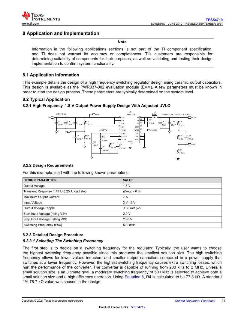
7.4.10 Small Signal Model For Frequency Compensation
The TPS54719 uses a transconductance amplifier for the error amplifier and readily supports two of the commonly used frequency compensation circuits. The compensation circuits are shown in Figure 7-11. The Type 2 circuits are most likely implemented in high bandwidth power supply designs using low-ESR output capacitors. In Type 2A, one additional high frequency pole is added to attenuate high frequency noise.
Vref
VO
R1
R3
C1
C2R2
CO
5pFRO
gmea COMP
VSENSE
Type 2A Type 2B
R3
C1
Figure 7-11. Types Of Frequency Compensation
The design guidelines for TPS54719 loop compensation are as follows:
1. The modulator pole, fpmod, and the esr zero, fz1, must be calculated using Equation 14 and Equation 15. Derating the output capacitor (COUT) can be needed if the output voltage is a high percentage of the capacitor rating. Use the capacitor manufacturer information to derate the capacitor value. Use Equation 16 and Equation 17 to estimate a starting point for the crossover frequency, fc. Equation 16 is the geometric mean of the modulator pole and the esr zero and Equation 17 is the mean of modulator pole and the
www.ti.comTPS54719
SLVSB69C – JUNE 2012 – REVISED SEPTEMBER 2021
Copyright © 2021 Texas Instruments Incorporated Submit Document Feedback 19
Product Folder Links: TPS54719

switching frequency. Use the lower value of Equation 16 or Equation 17 as the maximum crossover frequency.
¦p ´ ´
Iout maxp mod =
2 Vout Cout (14)
¦p ´ ´
1z mod =
2 Resr Cout (15)
¦ ¦ ´ ¦C = p mod z mod (16)
¦¦ ¦ ´C
sw= p mod
2 (17)
2. R3 can be determined by
p ¦ ´ ´
´ ´
OUT
ea ps
2 × c Vo CR3 =
gm Vref gm (18)
where:
• gmea is the amplifier gain (250 μA/V)• gmps is the power stage gain (25 A/V)
3. Place a compensation zero at the dominant pole ¦
´ ´ pOUT L
1p =
C R 2 . C1 can be determined by
´L OUTR CC1 =
R3 (19)
4. C2 is optional. It can be used to cancel the zero from the ESR of Co.
´ OUTResr CC2 =
R3 (20)
TPS54719SLVSB69C – JUNE 2012 – REVISED SEPTEMBER 2021 www.ti.com
20 Submit Document Feedback Copyright © 2021 Texas Instruments Incorporated
Product Folder Links: TPS54719
8 Application and ImplementationNote
Information in the following applications sections is not part of the TI component specification, and TI does not warrant its accuracy or completeness. TI’s customers are responsible for determining suitability of components for their purposes, as well as validating and testing their design implementation to confirm system functionality.
8.1 Application InformationThis example details the design of a high frequency switching regulator design using ceramic output capacitors. This design is available as the PWR037-002 evaluation module (EVM). A few parameters must be known in order to start the design process. These parameters are typically determined on the system level.
8.2 Typical Application8.2.1 High Frequency, 1.8-V Output Power Supply Design With Adjusted UVLO
VIN= 3-6V VOUT= 1.8V , IOUT = 7 A maxTPS54719
C5
56pF
R3
5.49k
R2
11.5k
R1
14.3k
R4
78.7k
C8
0.1uF
R6
20k
C6
5600pF R7
10.0k
R5
51.1
C2
10uF
C3
0.1uF
C9
22uF
C7
0.01uF
1VIN
2VIN
3GND
4GND
5AGND
6VSNS
7COMP
8RT/CLK
9SS/TR
10PH
11PH
12PH
13BOOT
14PWRGD
15EN
16VIN
17
PWPD
U1
C11
270pF
C10
22uF
C4
220pF
L11.5uH
C1
10uF
VSNS
VSNS
VIN
VIN
ENPWRGD
VOUT
8.2.2 Design Requirements
For this example, start with the following known parameters:
DESIGN PARAMETER VALUEOutput Voltage 1.8 V
Transient Response 1.75 to 5.25 A load step ΔVout = 6 %
Maximum Output Current 7 A
Input Voltage 3 V - 6 V
Output Voltage Ripple < 30 mV p-p
Start Input Voltage (rising VIN) 2.9 V
Stop Input Voltage (falling VIN) 2.66 V
Switching Frequency (Fsw) 500 kHz
8.2.3 Detailed Design Procedure8.2.3.1 Selecting The Switching Frequency
The first step is to decide on a switching frequency for the regulator. Typically, the user wants to choose the highest switching frequency possible since this produces the smallest solution size. The high switching frequency allows for lower valued inductors and smaller output capacitors compared to a power supply that switches at a lower frequency. However, the highest switching frequency causes extra switching losses, which hurt the performance of the converter. The converter is capable of running from 200 kHz to 2 MHz. Unless a small solution size is an ultimate goal, a moderate switching frequency of 500 kHz is selected to achieve both a small solution size and a high efficiency operation. Using Equation 8, R4 is calculated to be 77.8 kΩ. A standard 1% 78.7-kΩ value was chosen in the design.
www.ti.comTPS54719
SLVSB69C – JUNE 2012 – REVISED SEPTEMBER 2021
Copyright © 2021 Texas Instruments Incorporated Submit Document Feedback 21
Product Folder Links: TPS54719

8.2.3.2 Output Inductor Selection
The inductor selected works for the entire TPS54719 input voltage range. To calculate the value of the output inductor, use Equation 21. KIND is a coefficient that represents the amount of inductor ripple current relative to the maximum output current. The inductor ripple current is filtered by the output capacitor. Therefore, choosing high inductor ripple currents impacts the selection of the output capacitor since the output capacitor must have a ripple current rating equal to or greater than the inductor ripple current. In general, the inductor ripple value is at the discretion of the designer; however, KIND is normally from 0.1 to 0.3 for the majority of applications.
For this design example, use KIND = 0.3 and the minimum inductor value is calculated to be 1.2 μH. For this design, a larger standard value of 1.5 μH was chosen. For the output filter inductor, it is important that the RMS current and saturation current ratings not be exceeded. The RMS and peak inductor current can be found from Equation 23 and Equation 24.
For this design, the RMS inductor current is 7.017 A and the peak inductor current is 7.84 A. The chosen inductor is a Würth 744311150 1.5 µH. It has a saturation current rating of 14 A (30% inductance loss) and an RMS current rating of 11 A ( 40 °C temperature rise). The series resistance is 6.6 mΩ typical.
The current flowing through the inductor is the inductor ripple current plus the output current. During power up, faults, or transient load conditions, the inductor current can increase above the calculated peak inductor current level calculated above. In transient conditions, the inductor current can increase up to the switch current limit of the device. For this reason, the most conservative approach is to specify an inductor with a saturation current rating equal to or greater than the switch current limit rather than the peak inductor current.
-´
´ ´ ¦
Vinmax Vout VoutL1 =
Io Kind Vinmax sw (21)
-´
´ ¦
Vinmax Vout VoutIripple =
L1 Vinmax sw (22)
æ ö´ -´ ç ÷´ ´ ¦è ø
22 1 Vo (Vinmax Vo)
ILrms = Io +12 Vinmax L1 sw (23)
IrippleILpeak = Iout +
2 (24)
8.2.3.3 Output Capacitor
There are three primary considerations for selecting the value of the output capacitor. The output capacitor determines the modulator pole, the output voltage ripple, and how the regulator responds to a large change in load current. The output capacitance needs to be selected based on the more stringent of these three criteria.
The desired response to a large change in the load current is the first criteria. The output capacitor needs to supply the load with current when the regulator can not. This situation would occur if there are desired hold-up times for the regulator where the output capacitor must hold the output voltage above a certain level for a specified amount of time after the input power is removed. The regulator is temporarily not able to supply sufficient output current if there is a large, fast increase in the current needs of the load, such as transitioning from no load to a full load. The regulator response to the load step change is limited by the control loop bandwidth, FCO. The output capacitor must be sized to supply the extra current without excessive output voltage drop until the control loop can respond to the load change. Equation 25 shows the minimum output capacitance necessary for an instantaneous load step change. Practical circuits will have a slew rate limited load step and will typically require less capacitance.
For this example, the transient load response is specified as a 6% change in Vout for a load step from 1.75 A (25%) to 5.25 A (75%), and ΔVout = 0.06 × 1.8 = 108 mV. For a load step slew rate of 30 mA / µsec, 2 × 22 µF is sufficient to meet the voltage drop requirement. The ESR of the output capacitor is ignored as the ESR of ceramic capacitors is small.
TPS54719SLVSB69C – JUNE 2012 – REVISED SEPTEMBER 2021 www.ti.com
22 Submit Document Feedback Copyright © 2021 Texas Instruments Incorporated
Product Folder Links: TPS54719
Equation 26 calculates the minimum output capacitance needed to meet the output voltage ripple specification. In this case, the maximum output voltage ripple is 30 mV. Under this requirement, Equation 26 yields 14 µF.
OUT
CO OUT
ICo >
F V
D
´ D (25)
1 1Co >
Voripple8 sw
Iripple
´´ ¦
(26)
where:
• ΔIout is the change in output current• Fsw is the regulators switching frequency• ΔVout is the allowable change in the output voltage• Vripple is the maximum allowable output voltage ripple• Iripple is the inductor ripple current
Equation 27 calculates the maximum ESR an output capacitor can have to meet the output voltage ripple specification. Equation 27 indicates the ESR should be less than 28.6 mΩ. In this case, the ESR of the ceramic capacitor is much less than 17.9 mΩ.
Additional capacitance de-ratings for aging, temperature and DC bias should be factored in which increases this minimum value. For this example, two 22-μF 10-V X5R ceramic capacitors with 3 mΩ of ESR are used.
Capacitors generally have limits to the amount of ripple current they can handle without failing or producing excess heat. An output capacitor that can support the inductor ripple current must be specified. Some capacitor data sheets specify the RMS (Root Mean Square) value of the maximum ripple current. Equation 28 can be used to calculate the RMS ripple current the output capacitor needs to support. For this application, Equation 28 yields 485 mA.
VorippleResr <
Iripple (27)
´ -
´ ´ ´ ¦
Vout (Vinmax Vout)Icorms =
12 Vinmax L1 sw (28)
8.2.3.4 Input Capacitor
The TPS54719 requires a high quality ceramic, type X5R or X7R, input decoupling capacitor of at least 10 μF of effective capacitance and in some applications a bulk capacitance. The effective capacitance includes any DC bias effects. The voltage rating of the input capacitor must be greater than the maximum input voltage. The capacitor must also have a ripple current rating greater than the maximum input current ripple of the TPS54719. The input ripple current can be calculated using Equation 29.
The value of a ceramic capacitor varies significantly over temperature and the amount of DC bias applied to the capacitor. The capacitance variations due to temperature can be minimized by selecting a dielectric material that is stable over temperature. X5R and X7R ceramic dielectrics are usually selected for power regulator capacitors because they have a high capacitance to volume ratio and are fairly stable over temperature. The output capacitor must also be selected with the DC bias taken into account. The capacitance value of a capacitor decreases as the DC bias across a capacitor increases.
For this example design, ceramic capacitors with at least a 10-V voltage rating are required to support the maximum input voltage. For this example, two 10-μF and one 0.1-μF, 10-V capacitors in parallel have been selected. The input capacitance value determines the input ripple voltage of the regulator. The input voltage ripple can be calculated using Equation 30. Using the design example values, Ioutmax = 7 A, Cin = 20 μF, and Fsw = 500 kHz, yields an input voltage ripple of 174 mV and a rms input ripple current of 3.43 A.
www.ti.comTPS54719
SLVSB69C – JUNE 2012 – REVISED SEPTEMBER 2021
Copyright © 2021 Texas Instruments Incorporated Submit Document Feedback 23
Product Folder Links: TPS54719
( )Vinmin VoutVoutIcirms = Iout
Vinmin Vinmin
-´ ´
(29)
Ioutmax 0.25Vin =
Cin sw
´D
´ ¦ (30)
8.2.3.5 Slow-Start Capacitor
The slow-start capacitor determines the minimum amount of time it takes for the output voltage to reach its nominal programmed value during power up. This is useful if a load requires a controlled voltage slew rate. This is also used if the output capacitance is very large and would require large amounts of current to quickly charge the capacitor to the output voltage level. The large currents necessary to charge the capacitor can make the TPS54719 reach the current limit or excessive current draw from the input power supply can cause the input voltage rail to sag. Limiting the output voltage slew rate solves both of these problems.
The slow-start capacitor value can be calculated using Equation 4. For the example circuit, the slow-start time is not too critical since the output capacitor value is 2 × 22 μF, which does not require much current to charge to 1.8 V. The example circuit has the slow start time set to an arbitrary value of 2.5 ms, which requires a 10-nF capacitor. In TPS54719, Iss is 2.4 μA and Vref is 0.6 V.
8.2.3.6 Bootstrap Capacitor Selection
A 0.1-μF ceramic capacitor must be connected between the BOOT to PH pin for proper operation. It is recommended to use a ceramic capacitor with X5R or better grade dielectric. The capacitor should have 10-V or higher voltage rating.
8.2.3.7 Undervoltage Lockout Set Point
The Undervoltage Lockout (UVLO) can be adjusted using an external voltage divider on the EN pin of the TPS54719. The UVLO has two thresholds: one for power up when the input voltage is rising and one for power down or brown outs when the input voltage is falling. For the example design, the supply should turn on and start switching once the input voltage increases above 2.794 V (VSTART). After the regulator starts switching, it should continue to do so until the input voltage falls below 2.595 V (VSTOP).
The programmable UVLO and enable voltages are set using a resistor divider between Vin and ground to the EN pin. Equation 2 and Equation 3 can be used to calculate the resistance values necessary. From Equation 2 and Equation 3, a 14.3 kΩ between VIN and EN and a 11.5 kΩ between EN and ground are required to produce the 2.794 and 2.595 volt start and stop voltages.
8.2.3.8 Output Voltage And Feedback Resistors Selection
For the example design, 20.0 kΩ was selected for R6. Using Equation 31, R7 is calculated as 10.0 kΩ.
-
VrefR7 = R6
Vo Vref (31)
Due to the internal design of the TPS54719, there is a minimum output voltage limit for any given input voltage. The output voltage can never be lower than the internal voltage reference of 0.6 V. Above 0.6 V, the output voltage may be limited by the minimum controllable on time. The minimum output voltage in this case is given by Equation 32.
( ) ( )( )ON DEADOUT(MIN) IN OUT DS L OUT DS
S S
t tV V I R R 0.7V I R
t t
æ ö= - + - - ´ç ÷
è ø (32)
where:
• VOUT(MIN) = minimum achievable output voltage• tON = minimum controllable on time (64 ns - 100 nsec typical)
TPS54719SLVSB69C – JUNE 2012 – REVISED SEPTEMBER 2021 www.ti.com
24 Submit Document Feedback Copyright © 2021 Texas Instruments Incorporated
Product Folder Links: TPS54719
• tS = 1/fSW (switching frequency)• tDEAD = dead time (70 nsec typical)• VIN = maximum input voltage• RDS = minimum high side MOSFET on resistance (26 - 35 mΩ)• IOUT = minimum load current• RL = series resistance of output inductor
There is also a maximum achievable output voltage which is limited by the minimum off time. The maximum output voltage is given by Equation 33
( ) ( )( )OFF DEADOUT(MAX) IN OUT DS L IN OUT DS
S S
t tV V 1 I R R V 0.7V I R
t t
æ ö= - - + - + - ´ç ÷
è ø (33)
where:
• VOUT(MAX) = maximum achievable output voltage• tS = 1/fSW (switching frequency)• tOFF = minimum off time (0 nsec typical)• tDEAD = dead time (70 nsec typical)• VIN = minimum input voltage• IOUT = maximum load current• RDS = maximum high side MOSFET on resistance (60 - 70 mΩ)• RL = series resistance of output inductor
8.2.3.9 Compensation
There are several possible methods to design closed loop compensation for dc/dc converters. For the ideal current mode control, the design equations can be easily simplified. The power stage gain is constant at low frequencies, and rolls off at -20 dB/decade above the modulator pole frequency. The power stage phase is 0 degrees at low frequencies and starts to fall one decade below the modulator pole frequency reaching a minimum of -90 degrees one decade above the modulator pole frequency. The modulator pole is a simple pole shown in Equation 34.
¦p ´ ´
Iout maxp mod =
2 Vout Cout (34)
For the TPS54719, most circuits will have relatively high amounts of slope compensation. As more slope compensation is applied, the power stage characteristics will deviate from the ideal approximations. The phase loss of the power stage will now approach -180 degrees, making compensation more difficult. The power stage transfer function can be solved but it is a tedious hand calculation that does not lend itself to simple approximations. It is best to use Pspice or TINA-TI to accurately model the power stage gain and phase so that a reliable compensation circuit can be designed. That is the technique used in this design procedure. Using the pspice model of (insert link here). Apply the values calculated previously to the output filter components of L1, C9 and C10. Set Rload to the appropriate value. For this design, L1 = 1.5 µH. C9 and C10 are set to 22 µF each, and the ESR is set to 3 mΩ. The Rload resistor is 1.8 V / 3.5 A = 514 mΩ for one half rated load. Now the power stage characteristic can be plotted as shown in Figure 8-1.
www.ti.comTPS54719
SLVSB69C – JUNE 2012 – REVISED SEPTEMBER 2021
Copyright © 2021 Texas Instruments Incorporated Submit Document Feedback 25
Product Folder Links: TPS54719
100 1000 10000 100000 1000000−60
−50
−40
−30
−20
−10
0
10
20
30
40
50
60
−180
−150
−120
−90
−60
−30
0
30
60
90
120
150
180
Frequency (Hz)
Gain
(dB
)
Phase (
°)
Gain
Phase
G006
Gain = 2.04 dB @ 50 kHz
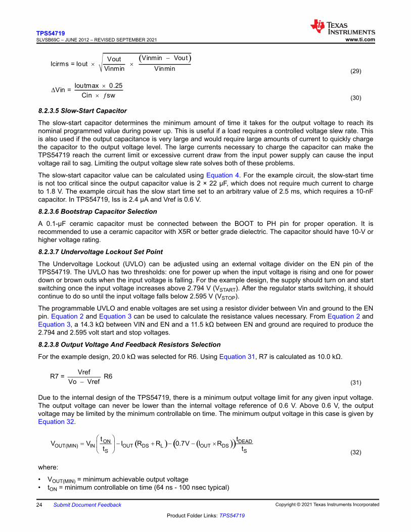
Figure 8-1. Power Stage Gain And Phase Characteristics
For this design, the intended crossover frequency is 50 kHz. From the power stage gain and phase plots, the gain at 50 kHz is 2.04 dB and the phase is about –135 degrees. For 60 degrees of phase margin, additional phase boost from a feedforward capacitor in parallel with the upper resistor of the voltage set point divider will be required. R3 sets the gain of the compensated error amplifier to be equal and opposite the power stage gain at crossover. The required value of R3 can be calculated from Equation 35.
-
×
PWRSTGG
20out
EA REF
V10R3 =
gm V (35)
To maximize phase gain, the compensator zero is placed one decade below the crossover frequency of 50 kHz. The required value for C6 is given by Equation 36.
CO
1C6 =
F2 R3
10× p × ×
(36)
To maximize phase gain the high frequency pole is placed one decade above the crossover frequency of 50 kHz. The pole can also be useful to offset the ESR of aluminum electrolytic output capacitors. The value for C5 can be calculated from Equation 37.
P
1C5 =
2 R3 F× p × × (37)
For maximum phase boost, the pole frequency FP will typically be one decade above the intended crossover frequency FCO.
The feedforward capacitor, C11, is used to increase the phase boost at crossover above what is normally available from Type II compensation. It places an additional zero/pole pair located at Equation 38 and Equation 39.
Z
1F =
2 C11 R6× p × × (38)
TPS54719SLVSB69C – JUNE 2012 – REVISED SEPTEMBER 2021 www.ti.com
26 Submit Document Feedback Copyright © 2021 Texas Instruments Incorporated
Product Folder Links: TPS54719
P
1F =
2 C11 R6 R7× p × × P (39)
This zero and pole pair is not independent. Once the zero location is chosen, the pole is fixed as well. For optimum performance, the zero and pole should be located symmetrically about the intended crossover frequency. The required value for C10 can calculated from Equation 40.
REFCO
OUT
1C11 =
V2 R6 F
V× p × × ×
(40)
For this design the calculated values for the compensation components are R3 = 5.49 kΩ, C6 = 5600 pF, C5 = 56 pF, and C11 = 270 pF.
8.2.4 Application Curves
0
10
20
30
40
50
60
70
80
90
100
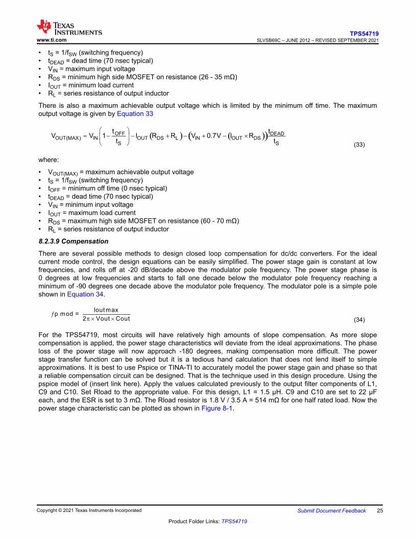
0 1 2 3 4 5 6 7
Output Current (A)
Effic
iency (
%)
VIN = 3.3 V
VIN = 5 V
G002
Figure 8-2. Efficiency vs Load Current
0
10
20
30
40
50
60
70
80
90
100
0.01 0.1 1 10
Output Current (A)
Effic
iency (
%)
VIN = 3.3 V
VIN = 5 V
G003
Figure 8-3. Efficiency vs Load Current
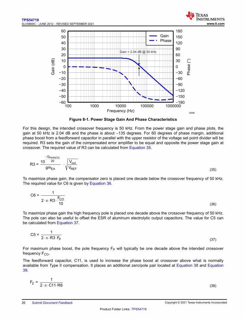
V = 100 mV / div (ac coupled)OUT
Time = 500 µsec / div
I = 2 A / divOUT
Load step = 1.75 - 5.25 A, slew rate = 30 mA / µsec
Figure 8-4. Transient Response, 3.5 A Step
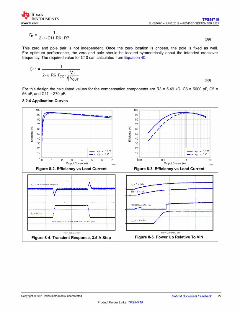
V = 1 V / divOUT
Time = 2 msec / div
EN = 2 V / div
V = 5 V / divIN
PWRGD = 5 V / div
Figure 8-5. Power Up Relative To VIN
www.ti.comTPS54719
SLVSB69C – JUNE 2012 – REVISED SEPTEMBER 2021
Copyright © 2021 Texas Instruments Incorporated Submit Document Feedback 27
Product Folder Links: TPS54719

V = 1 V / divOUT
Time = 2 msec / div
EN = 2 V / div
V = 5 V / divIN
PWRGD = 5 V / div
Figure 8-6. Power Down Relative To VIN
V = 1 V / divOUT
Time = 2 msec / div
EN = 2 V / div
V = 5 V / divIN
PWRGD = 5 V / div
Figure 8-7. Power Up Relative To EN
V = 1 V / divOUT
Time = 200 µsec / div
EN = 2 V / div
V = 5 V / divIN
PWRGD = 5 V / div
Figure 8-8. Power Down Relative To EN
V = 20 mV / div (ac coupled)OUT
Time = 1 µsec / div
PH = 2 V / div
Figure 8-9. Output Ripple, IOUT = 7 A
V = 100 mV / div (ac coupled)IN
Time = 1 µsec / div
PH = 2 V / div
Figure 8-10. Input Ripple, IOUT = 7 A
100 1000 10000 100000 1000000−60
−50
−40
−30
−20
−10
0
10
20
30
40
50
60
−180
−150
−120
−90
−60
−30
0
30
60
90
120
150
180
Frequency (Hz)
Gain
(dB
)
Phase (
°)
Gain
Phase
G001
Figure 8-11. Closed Loop Response, VIN = 5 V, IOUT = 3.5 A
TPS54719SLVSB69C – JUNE 2012 – REVISED SEPTEMBER 2021 www.ti.com
28 Submit Document Feedback Copyright © 2021 Texas Instruments Incorporated
Product Folder Links: TPS54719
−0.5
−0.4
−0.3
−0.2
−0.1
0
0.1
0.2
0.3
0.4
0.5
0 1 2 3 4 5 6 7
Output Current (A)
Outp
ut V
oltage D
evia
tion (
%)
VIN = 3.3 V
VIN = 5 V
G005
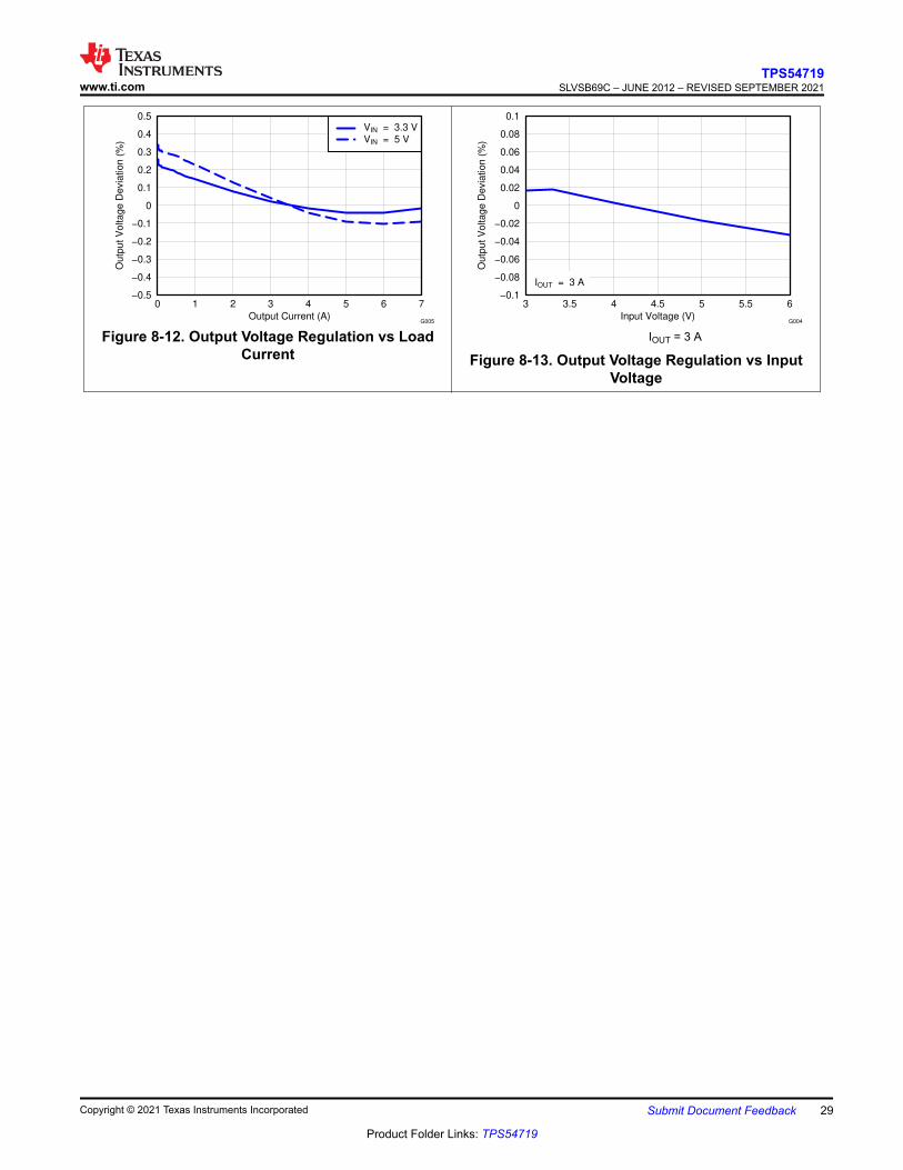
Figure 8-12. Output Voltage Regulation vs Load Current
−0.1
−0.08
−0.06
−0.04
−0.02
0
0.02
0.04
0.06
0.08
0.1
3 3.5 4 4.5 5 5.5 6
Input Voltage (V)
Outp
ut V
oltage D
evia
tion (
%)
IOUT = 3 A
G004
IOUT = 3 A
Figure 8-13. Output Voltage Regulation vs Input Voltage
www.ti.comTPS54719
SLVSB69C – JUNE 2012 – REVISED SEPTEMBER 2021
Copyright © 2021 Texas Instruments Incorporated Submit Document Feedback 29
Product Folder Links: TPS54719
9 Power Supply RecommendationsThe input voltage for VIN pin should be well controlled to avoid exceeding the maximum voltage rating of 7 V; otherwise, the device can have risk of damage.
10 Layout10.1 Layout GuidelinesLayout is a critical portion of good power supply design. There are several signal paths that conduct fast changing currents or voltages that can interact with stray inductance or parasitic capacitance to generate noise or degrade the power supplies performance. Care should be taken to minimize the loop area formed by the bypass capacitor connections and the VIN pins. See Figure 10-1 for a PCB layout example. The GND pins and AGND pin should be tied directly to the power pad under the IC. The power pad should be connected to any internal PCB ground planes using multiple vias directly under the IC. Additional vias can be used to connect the top side ground area to the internal planes near the input and output capacitors. For operation at full rated load, the top side ground area along with any additional internal ground planes must provide adequate heat dissipating area.
Locate the input bypass capacitor as close to the IC as possible. The PH pin should be routed to the output inductor. Since the PH connection is the switching node, the output inductor should be located very close to the PH pins, and the area of the PCB conductor minimized to prevent excessive capacitive coupling. The boot capacitor must also be located close to the device. The sensitive analog ground connections for the feedback voltage divider, compensation components, slow start capacitor and frequency set resistor should be connected to a separate analog ground trace as shown. The RT pin is particularly sensitive to noise so the RT resistor should be located as close as possible to the IC and routed with minimal lengths of trace. The additional external components can be placed approximately as shown. It may be possible to obtain acceptable performance with alternate PCB layouts, however this layout has been shown to produce good results and is meant as a guideline.
TPS54719SLVSB69C – JUNE 2012 – REVISED SEPTEMBER 2021 www.ti.com
30 Submit Document Feedback Copyright © 2021 Texas Instruments Incorporated
Product Folder Links: TPS54719

10.2 Layout Example
VIN
VIN
VIN
GND
EN
GND
VS
EN
SE
SS/TR
PH
PH
PH
PW
RG
D
BO
OT
RT
CO
MP
AG
ND
PH
BOOT
CAPACITOR
VOUTOUTPUT
INDUCTOR
OUTPUT
FILTER
CAPACITOR
SLOW START
CAPACITOR
COMPENSATION
NETWORK
TOPSIDE
GROUND
AREA
VIA to Ground Plane
FREQUENCY
SET
RESISTOR
ANALOG
GROUND
TRACE
VIN
INPUT
BYPASS
CAPACITOR
VIN
UVLO SET
RESISTORS
FEEDBACK
RESISTORS
VIA to
Ground
Plane
EXPOSED
POWERPAD
AREA
Figure 10-1. PCB Layout Example
www.ti.comTPS54719
SLVSB69C – JUNE 2012 – REVISED SEPTEMBER 2021
Copyright © 2021 Texas Instruments Incorporated Submit Document Feedback 31
Product Folder Links: TPS54719
10.2.1 Power Dissipation Estimate
The following formulas show how to estimate the IC power dissipation under continuous conduction mode (CCM) operation. The power dissipation of the IC (Ptot) includes the following:
• Conduction loss (Pcon)• Dead time loss (Pd)• Switching loss (Psw)• Gate drive loss (Pgd)• Supply current loss (Pq)
Pcon = Io2 × Rdson_temp
Pd = ƒsw × Iout × 0.7 × 70 × 10-9
Psw = 0.5 × Vin × Io × ƒsw × 9 × 10⁻⁹
Pgd = 2 × Vin × 6 × 10⁻⁹ × ƒsw
Pq = 455 × 10-6 × Vin
where:
• IOUT is the output current (A)• Rdson is the on-resistance of the high-side MOSFET (Ω)• VIN is the input voltage (V)• ƒsw is the switching frequency (Hz)
So
Ptot = Pcon + Pd + Psw + Pgd + Pq
For given TA,
TJ = TA + Rth × Ptot
For given TJMAX = 140°C
TAmax = TJMAX – Rth × Ptot
where:
• Ptot is the total device power dissipation (W)• TA is the ambient temperature (°C)• TJ is the junction temperature (°C)• Rth is the thermal resistance of the package (°C/W)• TJMAX is maximum junction temperature (°C)• TAMAX is maximum ambient temperature (°C)
There are additional power losses in the regulator circuit due to the inductor AC and DC losses and trace resistance that impact the overall efficiency of the regulator.
TPS54719SLVSB69C – JUNE 2012 – REVISED SEPTEMBER 2021 www.ti.com
32 Submit Document Feedback Copyright © 2021 Texas Instruments Incorporated
Product Folder Links: TPS54719
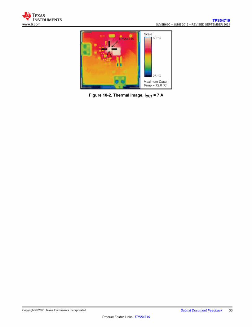
60 °C
25 °C
Maximum CaseTemp = 72.8 °C
Scale
TPS54719
Figure 10-2. Thermal Image, IOUT = 7 A
www.ti.comTPS54719
SLVSB69C – JUNE 2012 – REVISED SEPTEMBER 2021
Copyright © 2021 Texas Instruments Incorporated Submit Document Feedback 33
Product Folder Links: TPS54719

11 Device and Documentation Support11.1 Receiving Notification of Documentation UpdatesTo receive notification of documentation updates, navigate to the device product folder on ti.com. Click on Subscribe to updates to register and receive a weekly digest of any product information that has changed. For change details, review the revision history included in any revised document.
11.2 Support ResourcesTI E2E™ support forums are an engineer's go-to source for fast, verified answers and design help — straight from the experts. Search existing answers or ask your own question to get the quick design help you need.
Linked content is provided "AS IS" by the respective contributors. They do not constitute TI specifications and do not necessarily reflect TI's views; see TI's Terms of Use.
11.3 TrademarksWEBENCH™ and TI E2E™ are trademarks of Texas Instruments.All trademarks are the property of their respective owners.11.4 Electrostatic Discharge Caution
This integrated circuit can be damaged by ESD. Texas Instruments recommends that all integrated circuits be handled with appropriate precautions. Failure to observe proper handling and installation procedures can cause damage.ESD damage can range from subtle performance degradation to complete device failure. Precision integrated circuits may be more susceptible to damage because very small parametric changes could cause the device not to meet its published specifications.
11.5 GlossaryTI Glossary This glossary lists and explains terms, acronyms, and definitions.
12 Mechanical, Packaging, and Orderable InformationThe following pages include mechanical, packaging, and orderable information. This information is the most current data available for the designated devices. This data is subject to change without notice and revision of this document. For browser-based versions of this data sheet, refer to the left-hand navigation.
TPS54719SLVSB69C – JUNE 2012 – REVISED SEPTEMBER 2021 www.ti.com
34 Submit Document Feedback Copyright © 2021 Texas Instruments Incorporated
Product Folder Links: TPS54719
PACKAGE OPTION ADDENDUM
www.ti.com 30-Aug-2021
Addendum-Page 1
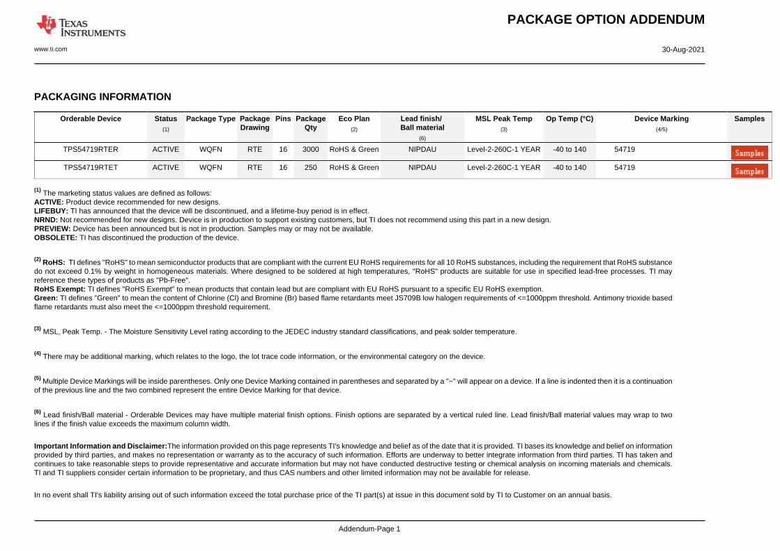
PACKAGING INFORMATION
Orderable Device Status(1)
Package Type PackageDrawing
Pins PackageQty
Eco Plan(2)
Lead finish/Ball material
(6)
MSL Peak Temp(3)
Op Temp (°C) Device Marking(4/5)
Samples
TPS54719RTER ACTIVE WQFN RTE 16 3000 RoHS & Green NIPDAU Level-2-260C-1 YEAR -40 to 140 54719
TPS54719RTET ACTIVE WQFN RTE 16 250 RoHS & Green NIPDAU Level-2-260C-1 YEAR -40 to 140 54719
(1) The marketing status values are defined as follows:ACTIVE: Product device recommended for new designs.LIFEBUY: TI has announced that the device will be discontinued, and a lifetime-buy period is in effect.NRND: Not recommended for new designs. Device is in production to support existing customers, but TI does not recommend using this part in a new design.PREVIEW: Device has been announced but is not in production. Samples may or may not be available.OBSOLETE: TI has discontinued the production of the device.
(2) RoHS: TI defines "RoHS" to mean semiconductor products that are compliant with the current EU RoHS requirements for all 10 RoHS substances, including the requirement that RoHS substancedo not exceed 0.1% by weight in homogeneous materials. Where designed to be soldered at high temperatures, "RoHS" products are suitable for use in specified lead-free processes. TI mayreference these types of products as "Pb-Free".RoHS Exempt: TI defines "RoHS Exempt" to mean products that contain lead but are compliant with EU RoHS pursuant to a specific EU RoHS exemption.Green: TI defines "Green" to mean the content of Chlorine (Cl) and Bromine (Br) based flame retardants meet JS709B low halogen requirements of <=1000ppm threshold. Antimony trioxide basedflame retardants must also meet the <=1000ppm threshold requirement.
(3) MSL, Peak Temp. - The Moisture Sensitivity Level rating according to the JEDEC industry standard classifications, and peak solder temperature.
(4) There may be additional marking, which relates to the logo, the lot trace code information, or the environmental category on the device.
(5) Multiple Device Markings will be inside parentheses. Only one Device Marking contained in parentheses and separated by a "~" will appear on a device. If a line is indented then it is a continuationof the previous line and the two combined represent the entire Device Marking for that device.
(6) Lead finish/Ball material - Orderable Devices may have multiple material finish options. Finish options are separated by a vertical ruled line. Lead finish/Ball material values may wrap to twolines if the finish value exceeds the maximum column width.
Important Information and Disclaimer:The information provided on this page represents TI's knowledge and belief as of the date that it is provided. TI bases its knowledge and belief on informationprovided by third parties, and makes no representation or warranty as to the accuracy of such information. Efforts are underway to better integrate information from third parties. TI has taken andcontinues to take reasonable steps to provide representative and accurate information but may not have conducted destructive testing or chemical analysis on incoming materials and chemicals.TI and TI suppliers consider certain information to be proprietary, and thus CAS numbers and other limited information may not be available for release.
In no event shall TI's liability arising out of such information exceed the total purchase price of the TI part(s) at issue in this document sold by TI to Customer on an annual basis.
PACKAGE OPTION ADDENDUM
www.ti.com 30-Aug-2021
Addendum-Page 2
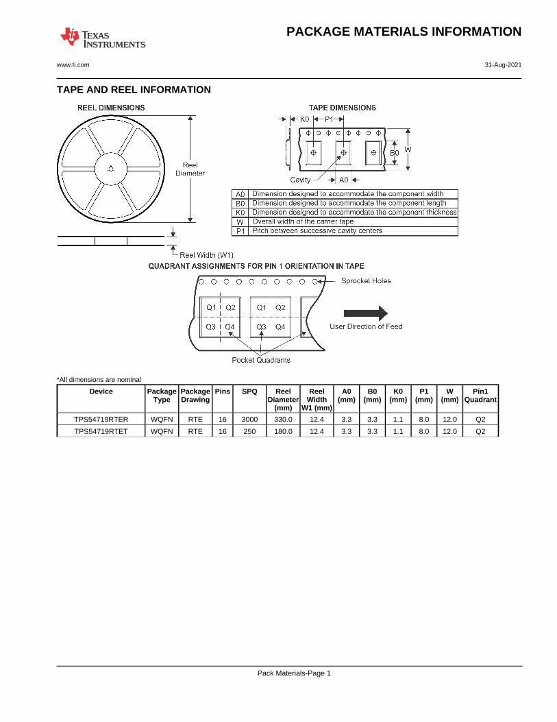
TAPE AND REEL INFORMATION
*All dimensions are nominal
Device PackageType
PackageDrawing
Pins SPQ ReelDiameter
(mm)
ReelWidth
W1 (mm)
A0(mm)
B0(mm)
K0(mm)
P1(mm)
W(mm)
Pin1Quadrant
TPS54719RTER WQFN RTE 16 3000 330.0 12.4 3.3 3.3 1.1 8.0 12.0 Q2
TPS54719RTET WQFN RTE 16 250 180.0 12.4 3.3 3.3 1.1 8.0 12.0 Q2
PACKAGE MATERIALS INFORMATION
www.ti.com 31-Aug-2021
Pack Materials-Page 1
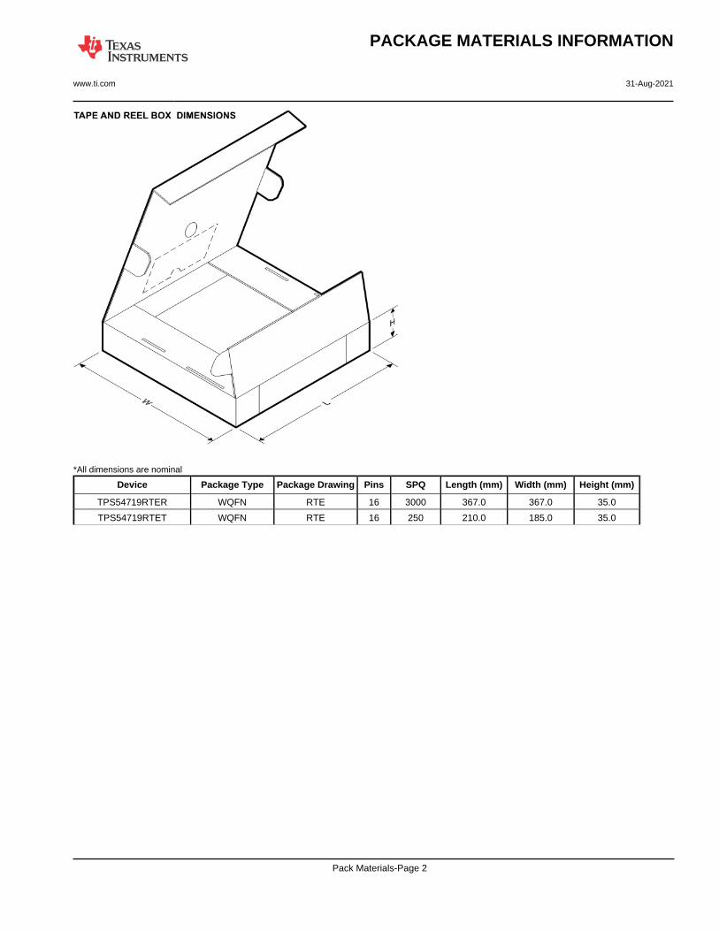
*All dimensions are nominal
Device Package Type Package Drawing Pins SPQ Length (mm) Width (mm) Height (mm)
TPS54719RTER WQFN RTE 16 3000 367.0 367.0 35.0
TPS54719RTET WQFN RTE 16 250 210.0 185.0 35.0
PACKAGE MATERIALS INFORMATION
www.ti.com 31-Aug-2021
Pack Materials-Page 2

www.ti.com
GENERIC PACKAGE VIEW
This image is a representation of the package family, actual package may vary.Refer to the product data sheet for package details.
WQFN - 0.8 mm max heightRTE 16PLASTIC QUAD FLATPACK - NO LEAD3 x 3, 0.5 mm pitch
4225944/A

www.ti.com
PACKAGE OUTLINE
C
16X 0.300.18
1.65 0.1
16X 0.50.3
0.80.7
(0.1) TYP
0.050.00
12X 0.5
4X1.5
A 3.12.9
B
3.12.9
WQFN - 0.8 mm max heightRTE0016FPLASTIC QUAD FLATPACK - NO LEAD
4219119/A 03/2018
PIN 1 INDEX AREA
0.08
SEATING PLANE
1
49
12
5 8
16 13(OPTIONAL)
PIN 1 ID 0.1 C A B0.05
EXPOSEDTHERMAL PAD
17 SYMM
SYMM
NOTES: 1. All linear dimensions are in millimeters. Any dimensions in parenthesis are for reference only. Dimensioning and tolerancing per ASME Y14.5M. 2. This drawing is subject to change without notice. 3. The package thermal pad must be soldered to the printed circuit board for thermal and mechanical performance.
SCALE 3.600
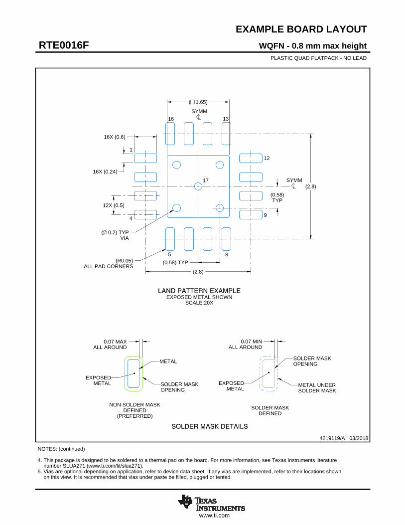
www.ti.com
EXAMPLE BOARD LAYOUT
0.07 MINALL AROUND
0.07 MAXALL AROUND
16X (0.24)
16X (0.6)
( 0.2) TYPVIA
12X (0.5)
(2.8)
(2.8)
(0.58)TYP
( 1.65)
(R0.05)ALL PAD CORNERS
(0.58) TYP
WQFN - 0.8 mm max heightRTE0016FPLASTIC QUAD FLATPACK - NO LEAD
4219119/A 03/2018
SYMM
1
4
5 8
9
12
1316
SYMM
LAND PATTERN EXAMPLEEXPOSED METAL SHOWN
SCALE:20X
17
NOTES: (continued) 4. This package is designed to be soldered to a thermal pad on the board. For more information, see Texas Instruments literature number SLUA271 (www.ti.com/lit/slua271).5. Vias are optional depending on application, refer to device data sheet. If any vias are implemented, refer to their locations shown on this view. It is recommended that vias under paste be filled, plugged or tented.
SOLDER MASKOPENING
METAL UNDERSOLDER MASK
SOLDER MASKDEFINED
EXPOSEDMETAL
METAL
SOLDER MASKOPENING
SOLDER MASK DETAILS
NON SOLDER MASKDEFINED
(PREFERRED)
EXPOSEDMETAL
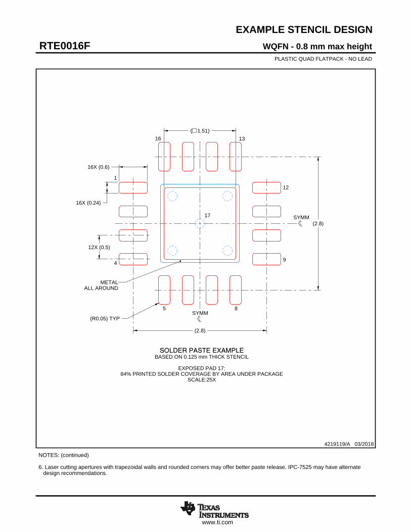
www.ti.com
EXAMPLE STENCIL DESIGN
16X (0.6)
16X (0.24)
12X (0.5)
(2.8)
(2.8)
( 1.51)
(R0.05) TYP
WQFN - 0.8 mm max heightRTE0016FPLASTIC QUAD FLATPACK - NO LEAD
4219119/A 03/2018
NOTES: (continued) 6. Laser cutting apertures with trapezoidal walls and rounded corners may offer better paste release. IPC-7525 may have alternate design recommendations.
SYMM
ALL AROUNDMETAL
SOLDER PASTE EXAMPLEBASED ON 0.125 mm THICK STENCIL
EXPOSED PAD 17:
84% PRINTED SOLDER COVERAGE BY AREA UNDER PACKAGESCALE:25X
SYMM
1
4
5 8
9
12
1316
17

IMPORTANT NOTICE AND DISCLAIMERTI PROVIDES TECHNICAL AND RELIABILITY DATA (INCLUDING DATA SHEETS), DESIGN RESOURCES (INCLUDING REFERENCE DESIGNS), APPLICATION OR OTHER DESIGN ADVICE, WEB TOOLS, SAFETY INFORMATION, AND OTHER RESOURCES “AS IS” AND WITH ALL FAULTS, AND DISCLAIMS ALL WARRANTIES, EXPRESS AND IMPLIED, INCLUDING WITHOUT LIMITATION ANY IMPLIED WARRANTIES OF MERCHANTABILITY, FITNESS FOR A PARTICULAR PURPOSE OR NON-INFRINGEMENT OF THIRD PARTY INTELLECTUAL PROPERTY RIGHTS.These resources are intended for skilled developers designing with TI products. You are solely responsible for (1) selecting the appropriate TI products for your application, (2) designing, validating and testing your application, and (3) ensuring your application meets applicable standards, and any other safety, security, regulatory or other requirements.These resources are subject to change without notice. TI grants you permission to use these resources only for development of an application that uses the TI products described in the resource. Other reproduction and display of these resources is prohibited. No license is granted to any other TI intellectual property right or to any third party intellectual property right. TI disclaims responsibility for, and you will fully indemnify TI and its representatives against, any claims, damages, costs, losses, and liabilities arising out of your use of these resources.TI’s products are provided subject to TI’s Terms of Sale or other applicable terms available either on ti.com or provided in conjunction with such TI products. TI’s provision of these resources does not expand or otherwise alter TI’s applicable warranties or warranty disclaimers for TI products.TI objects to and rejects any additional or different terms you may have proposed. IMPORTANT NOTICE
Mailing Address: Texas Instruments, Post Office Box 655303, Dallas, Texas 75265Copyright © 2022, Texas Instruments Incorporated