tuning the properties of transparent oxide conductors...
TRANSCRIPT

Tuning the Properties of Transparent Oxide Conductors. DopantIon Size and Electronic Structure Effects on CdO-Based
Transparent Conducting Oxides. Ga- and In-Doped CdO ThinFilms Grown by MOCVD
Shu Jin,†,‡ Yu Yang,†,‡ Julia E. Medvedeva,§,⊥ Lian Wang,†,‡ Shuyou Li,†,‡
Norma Cortes,‡,# John R. Ireland,# Andrew W. Metz,†,‡ Jun Ni,†,‡ Mark C. Hersam,*,‡,#
Arthur J. Freeman,*,§ and Tobin J. Marks*,†,‡
Department of Chemistry, Materials Research Center, Department of Physics and Astronomy, andDepartment of Materials Science and Engineering, Northwestern UniVersity,
EVanston, Illinois 60208-3113, and Department of Physics, UniVersity of Missouri—Rolla,Rolla, Missouri 65409
ReceiVed September 11, 2007. ReVised Manuscript ReceiVed October 25, 2007
A combined experimental and theoretical/band structure investigation is reported of Ga-doped CdO (CGO)and In-doped CdO (CIO) thin films grown on both amorphous glass and single-crystal MgO(100) substratesat 410 °C by metal–organic chemical vapor deposition (MOCVD). Film phase structure, microstructure, andelectrical and optical properties are systematically investigated as a function of doping stoichiometry andgrowth conditions. XRD data reveal that all as-deposited CGO and CIO thin films are phase-pure andpolycrystalline, with features assignable to a cubic CdO-type crystal structure. Epitaxial films grown on single-crystal MgO(100) exhibit biaxial, highly textured microstructures. These as-deposited CGO and CIO thinfilms exhibit excellent optical transparency, with an average transmittance of >80% in the visible range. Gaand In doping widens the optical band gap from 2.85 to 3.08 and 3.18 eV, respectively, via a Burstein–Mossshift. On MgO(100), room temperature thin film conductivities of 11 500 and 20 000 S/cm are obtained at anoptimum Ga and In doping levels of 1.6% and 2.6%, respectively. Together, the experimental and theoreticalresults reveal that dopant ionic radius and electronic configuration have a significant influence on the CdO-based TCO structural, electronic, and optical properties: (1) lattice parameters contract as a function of dopantionic radius in the order Y (1.09 Å) < In (0.94 Å) < Sc (0.89 Å), Ga (0.76 Å), with the smallest radius ionamong the four dopants only shrinking the lattice marginally and exhibiting low doping efficiency; (2) carriermobilities and doping efficiencies decrease in the order In > Y > Sc > Ga; (3) the Sc and Y dopant d stateshave substantial influence on the position and width of the s-based conduction band, which ultimately determinesthe intrinsic charge transport characteristics.
Introduction
Transparent conducting oxides (TCOs) have gained signifi-cant attention over the past two decades, serving as keycomponents in optoelectronic devices such as flat panel displays(FPDs), organic light-emitting diodes (OLEDs), photovoltaics,solar cells, optical waveguides, and energy-efficient windows.1–13
Currently, tin-doped indium oxide (ITO), with a typical
electrical conductivity of (3–5) × 103 S/cm and 85–90%transparency in the visible region, is employed on a hugescale as a transparent electrode in many display technolo-gies. However, there are several important limitations thatcloud its future applicability: (1) limited availability andhigh cost of indium, (2) relatively low conductivity (notsuitable for large-area displays), (3) significant opticalabsorption in the blue-green region (not suitable for manyfull-color displays), and (4) chemical instability in certaindevice structures (e.g., corrosion in OLEDs). In view ofthese issues, intense research has focused on understandingfundamental TCO crystal structure–film microstructure–electronic structure–charge transport–optical transparency
* To whom correspondence should be addressed.† Department of Chemistry, Northwestern University.‡ Materials Research Center, Northwestern University.§ Department of Physics and Astronomy, Northwestern University.# Department of Materials Science and Engineering, Northwestern University.⊥ Current address: University of Missouri—Rolla.
(1) Coutts, T. J.; Mason, T. O.; Perkins, J. D.; Ginley, D. S. Proc.Electrochem. Soc. 1999, 99-11, 274.
(2) Coutts, T. J.; Young, D. L.; Li, X. MRS Symp. Proc. 2000, 623, 199.(3) Freeman, A. J.; Poeppelmeier, K. R.; Mason, T. O.; Chang, R. P. H.;
Marks, T. J. MRS Bull. 2000, 25, 45.(4) Ginley, D. S.; Bright, C. MRS Bull. 2000, 25, 15.(5) Gordon, R. G. MRS Bull. 2000, 25, 52.(6) Granqvist, C. G.; Hultaker, A. Thin Solid Films 2002, 411, 1.(7) Hosono, H.; Ohta, H.; Orita, M.; Ueda, K.; Hirano, M. Vacuum 2002,
66, 419.(8) Kawamura, K.; Takahashi, M.; Yagihara, M.; Nakayama, T. European
Patent Application, EP1271561, A2 20030102, CAN 138:81680, AN2003:4983, 2003.
(9) Kawazoe, H.; Yanagi, H.; Ueda, K.; Hosono, H. MRS Bull. 2000, 25,28.
(10) Lewis, B. G.; Paine, D. C. MRS Bull. 2000, 25, 22.(11) Mason, T. O.; Gonzalez, G. B.; Kammler, D. R.; Mansourian-Hadavi,
N.; Ingram, B. J. Thin Solid Films 2002, 411, 106.(12) Minami, T. MRS Bull. 2000, 25, 38.(13) Wu, X.; Dhere, R. G.; Albin, D. S.; Gessert, T. A.; DeHart, C.; Keane,
J. C.; Duda, A.; Coutts, T. J.; Asher, S.; Levi, D. H.; Moutinho, H. R.;Yan, Y.; Moriarty, T.; Johnston, S.; Emery, K.; Sheldon, P. Proc.NCPV Prog. ReV. Meet., Lakewood, CO 2001, 47.
220 Chem. Mater. 2008, 20, 220–230
10.1021/cm702588m CCC: $40.75 2008 American Chemical SocietyPublished on Web 12/12/2007

relationships and on searching for ITO alternatives thatare less expensive and possess comparable or higherconductivity and/or wider optical transparency win-dows.3,5,9,10,12,14–20
Recently, CdO-based TCOs have received much attentiondue to their exceptional carrier mobilities, nearly metallicconductivities, and relatively simple crystal structures.11,21–28
Sn doping of CdO thin films grown epitaxially on MgO(111)by pulsed laser deposition (PLD) achieves thin film mobilitiesand conductivities as high as 607 cm2/(V s) and 42 000 S/cm,respectively, rendering them the most conductive TCO thinfilms with the highest carrier mobilities reported to date.26
Although the optical band gap of pure bulk CdO is only 2.3eV,29 leading to relatively poor optical transparency in theshort wavelength range, aliovalent metal doping offers thepossibility of tuning the electronic structure and the opticalband gap through a carrier concentration-dependent Burstein–Moss (B–M) energy level shift.30,31 CdO, with a simple cubicrock salt structure, broadly dispersed s-like conduction band,and a small carrier effective mass, is considered to be anideal model material in which to study the effects of dopingon TCO band structure, crystal chemistry, and chargetransport.
Various deposition techniques, such as reactive evapora-tion,32,33 solution growth,34 spray pyrolysis,35,36 sputtering,37–40
PLD,26 and MOCVD,23,25,27,28,41–44 have been employed togrow CdO and CdO-based thin films. For device fabrication,chemical vapor deposition offers many attractive features,such as in situ growth under a variety of atmospheres, low-cost equipment, amenability to large area coverage with highthroughput, conformal coverage, easy control of growthchemistry, and the possibility of creating metastable phases.45
In previous work from this laboratory, undoped and dopedCdO thin films were successfully grown by MOCVD usingoptimized metal–organic Cd precursors.23,25,27,44 In-dopedCdO thin films grown on glass by MOCVD exhibit conduc-tivities as high as 16 800 S/cm. It was found that In-dopingdramatically alters the CdO band structure by extensivemixing of In 5s and Cd 5s states, also yielding a hybridizationgap in the conduction band.44 Sc3+ and Y3+ with six-coordinate ionic radii of 0.89 and 1.04 Å, respectively, wereemployed to test the dopant size effects.23,27 Compared toIn3+ and Sn4+, the s states of Sc3+ and Y3+ are locateddeeper in the conduction band, resulting in a weak hybridiza-tion with the Cd 5s states. Thus, these experiments also stroveto assess the role of these s states. It was found that thinfilm conductivities as high as 6000 and 8540 S/cm areobtained on glass substrates at 1.2% Sc and 1.2% Y doping,respectively. Compared to In-doped CdO, the Sc- andY-doped CdO (CSO, CYO) thin films on glass exhibit lowercarrier mobilities and carrier concentrations, in accord withthe lower dispersion of the s-like conduction band, asrevealed by first-principles FLAPW electronic band structurecalculations.23 CSO and CYO thin films on MgO(100) witha maximum conductivity of 18 100 and 17 800 S/cm areobtained at a Sc doping level of ∼1.8% and a Y doping levelof 1.3%, respectively, which are to date the most conductivetransparent conducting oxide materials grown by MOCVD.All of these MOCVD-derived thin films exhibit good opticaltransparency, with an average transmittance >80% in thevisible range. Sc and Y doping effectively widens the bandgap from 2.7 to 3.4 eV via a Burstein–Moss band-filling shift,in agreement with our screened exchange local densityapproximation (sX-LDA) calculations.23,27,46
Our continued interest in CdO-based TCOs focuses onunderstanding crystal structure–charge transport relation-ships by further doping CdO with a wide variety ofdopants which simultaneously offer (1) controlled latticeparameter excursions via varying the ionic radius and (2)varying degrees of orbital overlap between the orbitals
(14) Coutts, T. J.; Young, D. L.; Li, X.; Mulligan, W. P.; Wu, X. J. Vac.Sci. Technol., A 2000, 18, 2646.
(15) Coutts, T. J.; Young, D. L.; Li, X. N. MRS Bull. 2000, 25, 58.(16) Edwards, D. D.; Mason, T. O.; Sinkler, W.; Marks, L. D.; Goutenoire,
F.; Poeppelmeier, K. R. J. Solid State Chem. 1998, 140, 242.(17) Ott, A. W.; Chang, R. P. H. Mater. Chem. Phys. 1999, 58, 132.(18) Phillips, J. M.; Cava, R. J.; Thomas, G. A.; Carter, S. A.; Kwo, J.;
Siegrist, T.; Krajewski, J. J.; Marshall, J. H.; Peck, W. F.; Rapkine,D. H. Appl. Phys. Lett. 1995, 67, 2246.
(19) Wang, A. C.; Dai, J. Y.; Cheng, J. Z.; Chudzik, M. P.; Marks, T. J.;Chang, R. P. H.; Kannewurf, C. R. Appl. Phys. Lett. 1998, 73, 327.
(20) Wang, R. P.; King, L. L. H.; Sleight, A. W. J. Mater. Res. 1996, 11,1659.
(21) Asahi, R.; Wang, A.; Babcock, J. R.; Edleman, N. L.; Metz, A. W.;Lane, M. A.; Dravid, V. P.; Kannewurf, C. R.; Freeman, A. J.; Marks,T. J. Thin Solid Films 2002, 411, 101.
(22) Babcock, J. R.; Wang, A. C.; Metz, A. W.; Edleman, N. L.; Metz,M. V.; Lane, M. A.; Kannewurf, C. R.; Marks, T. J. Chem. Vap.Deposition 2001, 7, 239.
(23) Jin, S.; Yang, Y.; Medvedeva, J. E.; Ireland, J. R.; Metz, A. W.; Ni,J.; Kannewurf, C. R.; Freeman, A. J.; Marks, T. J. J. Am. Chem. Soc.2004, 126, 13787.
(24) Kammler, D. R.; Mason, T. O.; Young, D. L.; Coutts, T. J.; Ko, D.;Poeppelmeier, K. R.; Williamson, D. L. J. Appl. Phys. 2001, 90, 5979.
(25) Metz, A. W.; Ireland, J. R.; Zheng, J. G.; Lobo, R.; Yang, Y.; Ni, J.;Stern, C. L.; Dravid, V. P.; Bontemps, N.; Kannewurf, C. R.;Poeppelmeier, K. R.; Marks, T. J. J. Am. Chem. Soc. 2004, 126, 8477.
(26) Yan, M.; Lane, M.; Kannewurf, C. R.; Chang, R. P. H. Appl. Phys.Lett. 2001, 78, 2342.
(27) Yang, Y.; Jin, S.; Medvedeva, J. E.; Ireland, J. R.; Metz, A. W.; Ni,J.; Hersam, M. C.; Freeman, A. J.; Marks, T. J. J. Am. Chem. Soc.2005, 127, 8796.
(28) Zhao, Z. Y.; Morel, D. L.; Ferekides, C. S. Thin Solid Films 2002,413, 203.
(29) Koffyberg, F. P. Phys. ReV. B 1976, 13, 4470.(30) Burstein, E. Phys. ReV. 1954, 93, 632.(31) Moss, T. S. Proc. Phys. Soc. A 1954, 382, 775.(32) Phatak, G.; Lal, R. Thin Solid Films 1994, 245, 17.(33) Reddy, K. T. R.; Sravani, C.; Miles, R. W. J. Cryst. Growth 1998,
185, 1031.(34) Matsuura, N.; Johnson, D. J.; Amm, D. T. Thin Solid Films 1997,
295, 260.(35) Murthy, L. C. S.; Rao, K. Bull. Mater. Sci. 1999, 22, 953.(36) Vigil, O.; Vaillant, L.; Cruz, F.; Santana, G.; Morales-Acevedo, A.;
Contreras-Puente, G. Thin Solid Films 2000, 361, 53.(37) Chu, T. L.; Chu, S. S. J. Electron. Mater. 1990, 19, 1003.
(38) Gurumurugan, K.; Mangalaraj, D.; Narayandass, S. K.; Nakanishi, Y.;Hatanaka, Y. Appl. Surf. Sci. 1997, 113/114, 422.
(39) Lewin, R.; Howson, R. P.; Bishop, C. A.; Ridge, M. I. Vacuum 1986,36, 95.
(40) Subramanyam, T. K.; Uthanna, S.; Naidu, B. S. Phys. Scr. 1998, 57,317.
(41) Gulino, A.; Castelli, F.; Dapporto, P.; Rossi, P.; Fragala, I. Chem.Mater. 2002, 14, 704.
(42) Gulino, A.; Dapporto, P.; Rossi, P.; Fragala, I. Chem. Mater. 2002,14, 4955.
(43) Gulino, A.; Dapporto, P.; Rossi, P.; Fragala, I. Chem. Mater. 2002,14, 1441.
(44) Wang, A.; Babcock, J. R.; Edleman, N. L.; Metz, A. W.; Lane, M. A.;Asahi, R.; Dravid, V. P.; Kannewurf, C. R.; Freeman, A. J.; Marks,T. J. Proc. Natl. Acad. Sci. U. S.A. 2001, 98, 7113.
(45) Schulz, D. L.; Marks, T. J. In CVD of Non-metals; Rees, W. S., Ed.;VCH: New York; pp 39–150.
(46) Medvedeva, J. E.; Freeman, A. J. Europhys. Lett. 2005, 69, 583.
221Chem. Mater., Vol. 20, No. 1, 2008Ga- and In-Doped CdO Thin Films

that contribute to the conduction band near the Fermi leveland thus govern the transport properties. Hence, Ga3+,with a much smaller ionic radius than In3+ (0.76 Å vs0.94 Å) and fully occupied 3d band (unlike Sc3+ and Y3+),represents an ideal probe ion to examine dopant radiussize effects; furthermore, In3+, which was previouslyfound to be the optimum dopant for CdO thin films on anamorphous glass substrates and is theoretically predictedto be an ideal doping candidate,27,44 has never before beengrown epitaxially on single crystal substrates.
In this experimental and theoretical contribution, wereport the growth of Ga- and In-doped CdO (CGO, CIO)thin films on amorphous glass and single crystal MgO(100)substrates by MOCVD. The CGO and CIO thin film phasestructure, microstructure, and electrical and optical proper-ties are investigated in detail as a function of doping level,and growth parameters and are compared with CSO andCYO thin films. These results are correlated with first-principles full-potential linear augmented plane wave(FLAPW) electronic band structure calculations within thescreened-exchange local density approximation (sX-LDA)to treat both ground and excited states. It will be seenthat phase-pure CGO and CIO thin films exhibit conduc-tivities of 11 500 and 20 000 S/cm, respectively, at Gaand In doping levels of 1.6% and 2.6%, respectively.Moreover, all the as-deposited TCO thin films exhibit goodvisible region transparency, with an average transmittance>80%. These structural, charge transport, and opticalresults are completely understandable within the frame-work of the electronic structure calculations.
Experimental Section
MOCVD Precursors and Thin Film Growth. CdO-based thinfilm growth was carried out in the previously describedhorizontal, cold-wall MOCVD reactor.47 The volatile metal–or-ganic Cd precursor Cd(hfa)2(N,N-DE-N′ ,N′-DMEDA) (1) (hfa) hexafluoroacetylacetonate, N,N-DE-N′ ,N′-DMEDA ) N,N-diethyl-N′,N′-dimethylethyldnediamine) was prepared from high-purity Cd(NO3)2 · 4H2O (99.999%, Aldrich) and was triplyvacuum-sublimed.25 Ga(dpm)3 (2) and In(dpm)3 (3) (dpm )dipivaloymethanate) were prepared from Ga(NO3) ·4H2O (99.999%,Alfa Aesar) and In(NO3)3 (99.999%, Alfa Aesar) by literatureprocedures.48–50
For Ga- and In-doped CdO thin film growth, the precursorreservoir temperatures/Ar carrier gas flow rates were optimized atCd(hfa)2(N,N′-DE-N,N′-DMEDA), 85 °C/15 sccm; Ga(dpm)3, 92°C/6–40 sccm; In(dpm)3, 94–95 °C/5–20 sccm. The O2 oxidizinggas was introduced upstream at 400 sccm after bubbling throughdistilled water. A system operating pressure of 4.0 ( 0.1 Torr anda substrate temperature of 400 °C were maintained during the thinfilm deposition. Corning 1737F glass and polished single-crystalMgO(100) (a ) 4.216 Å) substrates were purchased from PrecisionGlass and Optics and MTI Corp., respectively. Both the glass and
the MgO(100) substrate surfaces were cleaned with acetone priorto the film deposition and were placed side-by-side on a SiC-coatedsusceptor in the growth reactor for simultaneous growth experiments.
Thin Film Physical Characterization Measurements. Com-position analyses of the present films were carried out usinginductively coupled plasma atomic emission spectrometry (ICP-AES). Optical transparency measurements were carried out in therange 300–3300 nm with a Cary 500 UV–vis–NIR spectrophotom-eter. Film thicknesses were measured using a Tencor P-10 profilo-meter after etching a step in the film using 5% HCl solution. X-raydiffraction θ–2θ scans of CdO films on glass were obtained witha Rigaku DMAX-A powder diffractometer using Ni-filtered Cu KRradiation. Rocking curves and � scans of the epitaxial thin filmson MgO(100) substrates were obtained on a home-built Rigaku four-circle diffractometer with detector-selected Cu KR radiation. Filmsurface morphology was imaged using a Digital InstrumentsNanoscope III atomic force microscope (AFM) operating in thecontact mode. Film microstructure was imaged on a Hitachi S4500FE scanning electron microscope (SEM). Transmission electronmicroscopy (TEM) images and selected area electron diffraction(SAED) patterns were obtained using a Hitachi 2000 microscopeoperating at 200 keV. Cross-sectional samples were prepared bymechanical grinding, dimpling, and ion milling. Ambient-temper-ature four-probe charge transport data were acquired on a Bio-RadHL5500 Hall effect measurement system. Variable-temperature Halleffect and four-probe conductivity data were collected between 77and 330 K and used instrumentation described previously.51
Theoretical Methods. First-principles electronic band structurecalculations on 12.5 atom % Ga-doped CdO were performed usingthe highly precise all-electron full-potential linearized augmentedplane wave (FLAPW) method52 that has no shape approximationfor the potential and charge density. The exchange-correlationpotential is treated via the local density approximation (LDA).Cutoffs of the plane-wave basis (14.4 Ry) and potential representa-tion (81.0 Ry) and expansion in terms of spherical harmonics withl e 8 inside the muffin-tin spheres were used. The equilibriumrelaxed geometry of the structures was determined via total energyand atomic force minimization for the lattice parameter, a, and theinternal atomic positions. Furthermore, to determine accurately theexcited-state band structure of CGO, we employed the self-consistent screened-exchange local density approximation (sX-
(47) Hinds, B. J.; McNeely, R. J.; Studebaker, D. B.; Marks, T. J.; Hogan,T. P.; Schindler, J. L.; Kannewurf, C. R.; Zhang, X. F.; Miller, D. J.J. Mater. Res. 1997, 12, 1214.
(48) Jablonski, Z.; Rychlowskahimmel, I.; Dyrek, M. Spectrochim. Acta,Part A 1979, 35, 1297.
(49) Utsunomi, K Bull. Chem. Soc. Jpn. 1971, 44, 2688.(50) Wang, A. C.; Edleman, N. L.; Babcock, J. R.; Marks, T. J.; Lane,
M. A.; Brazis, P. R.; Kannewurf, C. R. J. Mater. Res. 2002, 17, 3155.
(51) Lyding, J. W.; Marcy, H. O.; Marks, T. J.; Kannewurf, C. R. IEEETrans. Instrum. Meas. 1988, 37, 76.
(52) Cimino, A.; Marezio, M. Phys. Chem. Solids 1960, 17, 57.
222 Chem. Mater., Vol. 20, No. 1, 2008 Jin et al.

LDA)53 which is known to provide a considerably improveddescription of optical properties compared to the LDA. Cutoffparameters of 10.24 Ry in the wave vectors and l e 3 inside themuffin-tin spheres were used. Summations over the Brillouin zonewere carried out using 10 special k points in the irreducible wedge.
Results and Discussion
We first describe CGO and CIO thin film growth by anefficient MOCVD process. Then, CGO and CIO filmcomposition, morphology, microstructure, and epitaxy arecharacterized as a function of doping level using a broadarray of complementary physical techniques. In addition, filmoptical and electrical properties are investigated and com-pared with those of the Sc- and Y-doped CdO analoguesgrown by the same technique. In doing so, we demonstratethe tunability of the CdO-based TCO materials by varyingthe dopants and substrates to achieve optimized transparentconductor properties. These results are compared and con-trasted to those computed via first-principles band structuretechniques.
Film Growth. A series of conductive CGO and CIO thinfilms were grown on Corning 1737F glass and single crystalMgO(100) at 410 °C and under a 400 sccm O2 flow rate for2 h by MOCVD. The film growth rates were ∼1–2 nm/minon glass and ∼1.5–2.5 nm/min on MgO(100), which aresimilar to those established for Sc- and Y-doped CdO. TheGa and In doping levels can be varied from 0% to 6.0% and0% to 6.9%, respectively, by varying the Ga and In precursorreservoir temperatures and Ar carrier gas flow rates.
Film Composition, Morphology, Microstructure, andEpitaxy. X-ray diffraction θ-2θ scans were carried out from2θ ) 25° to 75°. Figure 1 shows XRD data as a function ofGa (Figure 1A) and In (Figure 1B) doping level. As can beseen from the figures, all of the films with Ga and In dopinglevels up to 6.0% and 6.9% are phase-pure, with a highlycrystalline FCC CdO structure. No Ga2O3, In2O3, or otherphases are detected by XRD, consistent with Ga3+ and In3+
substituting for the Cd2+ in the lattice instead of forming anew phase.
Using polycrystalline silicon as an internal calibrationreference, the precise lattice parameters of the MOCVD-derived CGO and CIO thin films on glass were determinedand are also compared with the results of Sc and Y dopingin Figure 2. It is found that the lattice parameters aregradually compressed with increasing Ga and In dopinglevels. Note that with the introduction of Ga the latticedimensions are not decreased as much as expected purelyon the basis of Vegard’s law dopant radius considerations,since six-coordinated Ga3+ with an ionic radius of 0.76 Åis far smaller than Cd2+ (1.09 Å). This suggests that the Gadoping efficiency is lower than for In, Sc, and Y, even thoughno new phase is formed. This trend is further supported bythe observation that the carrier concentration increases onlyslightly with increased Ga doping levels (see below). Inmarked contrast, In3+, having a six-coordinate ionic radiusof 0.94 Å (more comparable to that of Cd2+), compresses
the lattice monotonically with increased doping levels, andthe carrier concentration increase with In doping is consistentwith a significantly greater doping efficiency. Note, however,that even the significant lattice contractions caused byprogressive In doping fall below those estimated from simpleVegard’s law considerations (Figure 2). This effect is likelydue to compensation by the antibonding character of theconduction band formed from the Cd 5s and O 2p states asdiscussed previously.23,46
In contrast to the above results for growth on amorphousglass substrates, all CGO and CIO thin films grown onMgO(100) exhibit a highly (200) textured microstructure.
(53) Wimmer, E.; Krakauer, H.; Weinert, M.; Freeman, A. J. Phys. ReV. B1981, 24, 864.
Figure 1. θ-2θ X-ray diffractograms of CGO (A) and CIO (B) thin filmsgrown on glass at 410 °C by MOCVD as a function of Ga and In dopinglevel (given in atom %).
Figure 2. Lattice parameter changes as a function of dopant size and dopinglevel for Ga-, In-, Sc-, and Y-doped CdO thin films grown on glass. Linesthrough the data points are drawn as a guide to the eye.
223Chem. Mater., Vol. 20, No. 1, 2008Ga- and In-Doped CdO Thin Films

The texture of the thin films is shown in Figures 3 and 4.As can be seen from Figure 3, the rocking curves of thefilms show good out-of-plane alignment. The full width athalf-maximum (fwhm) increases from 0.5° for pure CdOfilms to 1.0° and 1.0° at 2.4% Ga and 2.6% In doping,
respectively, and to 1.8° and 1.4° at 6.0% Ga and 6.9% Indoping, respectively, indicating that the crystallinity decreaseswith increased Ga and In doping. Note that the In-dopedCdO thin films have the greatest crystallinity among the fourdopants studied. In-plane orientation was investigated by�-scans of the CdO (111) reflection at � ) 54.7°, and dataare shown in Figure 4. The clear 4-fold rotational symmetryof the CdO (111) reflections together with the small fwhms(0.5° for pure CdO, 1.2° for CGO at 2.4% Ga doping, 1.1°for CIO at 2.6% In doping) reveal excellent in-planeorientation of the films. The orientation relations betweenthe CGO and CIO thin films and the MgO(100) substratesare therefore CdO(100)||MgO(100).
TEM images and SAED patterns of 1.6% Ga-doped CdOfilms grown on MgO(100) are shown in Figure 5. The SAEDpattern of the film indicates that the CdO grains retain thebiaxial (in-plane and out-of-plane) texture of the single-crystal substrate. Figure 5B shows that the Ga-doped CdOthin films grow epitaxially with a highly textured crystallinity.The dark shadow on the interface of the TEM cross sectionindicates that most of the strain from the mismatch of thelattice (aMgO ) 4.216 Å, ∼10% smaller than aCdO ) 4.696Å) has relaxed at or near the interface.
SEM surface images in Figures 6 and 7 show that the as-deposited CGO and CIO thin films grown on glass are denselypacked with heavily grained structures. At low Ga and In dopinglevels (e3.2–3.3%), films on glass are all very uniform withrounded grains in plan view. With the Ga and In dopingincreased to 4.9% and 4.3%, respectively, and higher, the grains
Figure 3. XRD texture analyses of CGO (A) and CIO (B) thin films grownon single-crystal MgO(100) as a function of Ga and In doping level; rockingcurves measured on the CdO(200) XRD peak.
Figure 4. XRD texture analyses of CGO (A) and CIO (B) thin films grownon single-crystal MgO(100) as a function of Ga and In doping level: in-plane �-scans measured on the CdO (111) XRD peak with � ) 54.7°. Gaand In doping levels are given in atom %.
Figure 5. TEM images of 1.6% doped CGO thin film on MgO(100): (A)SAED pattern, (B) cross-section image (MgO substrate is on the left sideof the image and the Ga-doped CdO film grown is on the right side).
224 Chem. Mater., Vol. 20, No. 1, 2008 Jin et al.
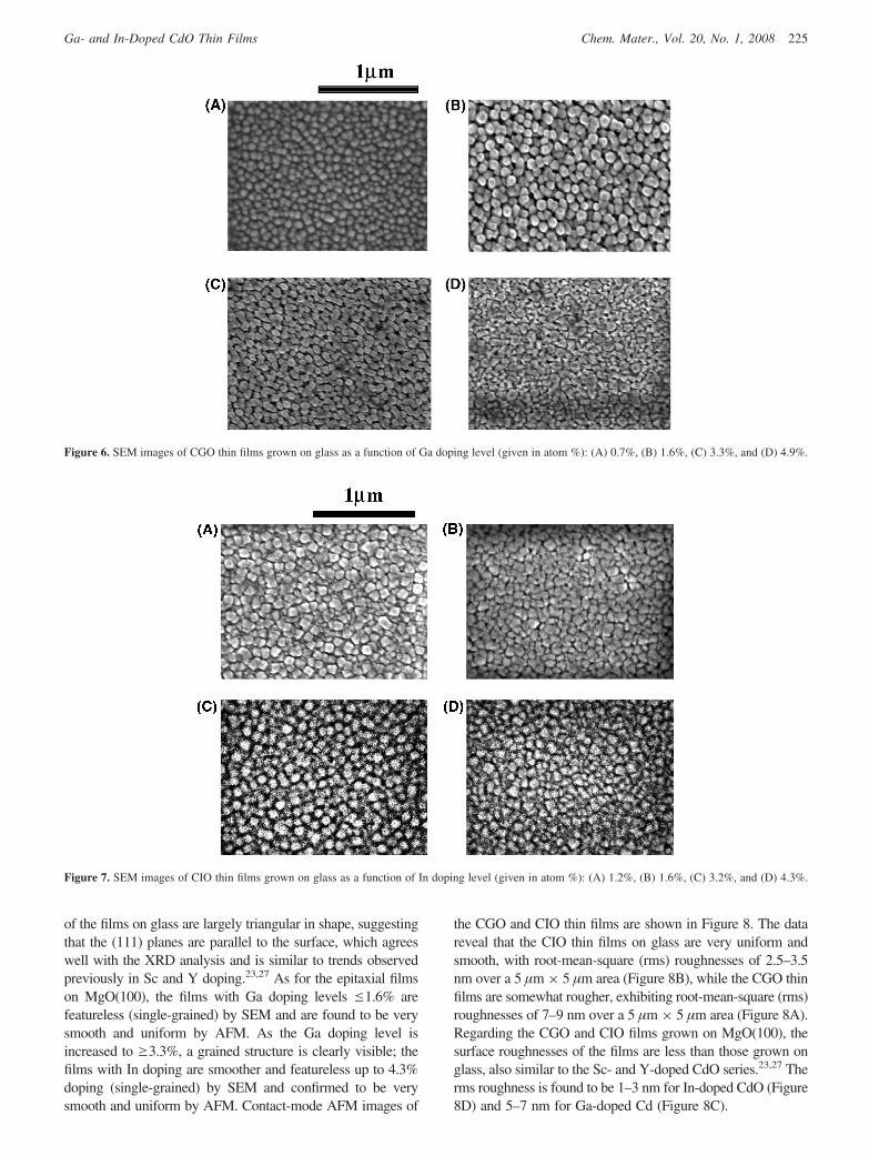
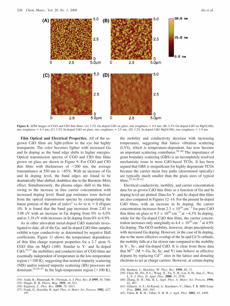
of the films on glass are largely triangular in shape, suggestingthat the (111) planes are parallel to the surface, which agreeswell with the XRD analysis and is similar to trends observedpreviously in Sc and Y doping.23,27 As for the epitaxial filmson MgO(100), the films with Ga doping levels e1.6% arefeatureless (single-grained) by SEM and are found to be verysmooth and uniform by AFM. As the Ga doping level isincreased to g3.3%, a grained structure is clearly visible; thefilms with In doping are smoother and featureless up to 4.3%doping (single-grained) by SEM and confirmed to be verysmooth and uniform by AFM. Contact-mode AFM images of
the CGO and CIO thin films are shown in Figure 8. The datareveal that the CIO thin films on glass are very uniform andsmooth, with root-mean-square (rms) roughnesses of 2.5–3.5nm over a 5 µm × 5 µm area (Figure 8B), while the CGO thinfilms are somewhat rougher, exhibiting root-mean-square (rms)roughnesses of 7–9 nm over a 5 µm × 5 µm area (Figure 8A).Regarding the CGO and CIO films grown on MgO(100), thesurface roughnesses of the films are less than those grown onglass, also similar to the Sc- and Y-doped CdO series.23,27 Therms roughness is found to be 1–3 nm for In-doped CdO (Figure8D) and 5–7 nm for Ga-doped Cd (Figure 8C).
Figure 6. SEM images of CGO thin films grown on glass as a function of Ga doping level (given in atom %): (A) 0.7%, (B) 1.6%, (C) 3.3%, and (D) 4.9%.
Figure 7. SEM images of CIO thin films grown on glass as a function of In doping level (given in atom %): (A) 1.2%, (B) 1.6%, (C) 3.2%, and (D) 4.3%.
225Chem. Mater., Vol. 20, No. 1, 2008Ga- and In-Doped CdO Thin Films
Film Optical and Electrical Properties. All of the as-grown CdO films are light-yellow to the eye but highlytransparent. The color becomes lighter with increased Gaand In doping as the band edge shifts to higher energies.Optical transmission spectra of CGO and CIO thin filmsgrown on glass are shown in Figure 9. For CGO and CIOthin films with thicknesses of ∼200 nm, the averagetransmittance at 550 nm is ∼85%. With an increase of Gaand In doping level, the band edges are found to bedramatically blue-shifted, doubtless due to the Burstein–Mosseffect. Simultaneously, the plasma edges shift to the blue,owing to the increase in free carrier concentration withincreased doping level. Band gap estimates were derivedfrom the optical transmission spectra by extrapolating thelinear portion of the plot of (Rhν)2 vs hν to R ) 0 (Figure10). It is found that the band gap increases from 2.85 to3.08 eV with an increase in Ga doping from 0% to 6.0%and to 3.18 eV with increases in In doping from 0% to 6.9%.
As in other ailovalent metal-doped CdO materials inves-tigated to date, all of the Ga- and In-doped CdO film samplesexhibit n-type conductivity as determined by negative Hallcoefficients. Figure 11 shows the temperature dependenceof thin film charge transport properties for a 2.7 atom %CGO film on MgO (100). Similar to Y- and Sc-dopedCdO,23,27 the mobilities and conductivities of CGO films areessentially independent of temperature in the low-temperatureregion (<100 K), suggesting that neutral impurity scattering(NIS) and/or ionized impurity scattering (IIS) processes aredominant.25,54–57 In the high-temperature region (>100 K),
the mobility and conductivity decrease with increasingtemperature, suggesting that lattice vibration scattering(LVS), which is temperature-dependent, has now becomean important scattering contributor.58–60 The importance ofgrain boundary scattering (GBS) is an incompletely resolvedmechanistic issue in most CdO-based TCOs. It has beenargued that GBS is insignificant for highly degenerate TCOsbecause the carrier mean free paths (determined optically)are typically much smaller than the grain sizes of typicalfilms.25,54,59–62
Electrical conductivity, mobility, and carrier concentrationdata for as-grown CdO thin films as a function of Ga and Indoping level are plotted. Data for Y- and Sc-doped thin filmsare also compared in Figures 12–14. For the present In-dopedCdO films, with an increase in In doping, the carrierconcentration increases from 2.3 × 1020 cm-3 for pure CdOthin films on glass to 9.3 × 1020 cm-3 at ∼4.3% In doping,while for the Ga-doped CdO thin films, the carrier concen-tration increases only marginally to 4.4 × 1020 cm-3 at 4.9%Ga doping. The GCO mobility, however, drops precipitouslywith increased Ga doping. However, in the case of In doping,due to the more effective overlap of the In and Cd 5s orbitals,the mobility falls at a far slower rate compared to the mobilityin Y-, Sc-, and Ga-doped CdO. It is clear from these datathat M3+ (M ) Ga, In, Sc, and Y) ions behave as effectivedopants by replacing Cd2+ sites in the lattice and donatingelectrons to act as charge carriers. However, at certain doping
(54) Asahi, R.; Mannstadt, W.; Freeman, A. J. Phys. ReV. B 1999, 59, 7486.(55) Dingle, R. B. Philos. Mag. 1955, 46, 831.(56) Erginsoy, C. Phys. ReV. 1950, 79, 1013.(57) Frank, G.; Koestlin, H. Appl. Phys. A: Mater. Sci. Process. 1982, A27,
197.
(58) Bardeen, J.; Shockley, W. Phys. ReV. 1950, 80, 72.(59) Chen, M.; Pei, Z. L.; Wang, X.; Yu, Y. H.; Liu, X. H.; Sun, C.; Wen,
L. S. J. Phys. D: Appl. Phys. 2000, 33, 2538.(60) Zhang, D. H.; Ma, H. L. Appl. Phys. A: Mater. Sci. Process. 1996,
62, 487.(61) Gilmore, A. S.; Al-Kaoud, A.; Kaydanov, V.; Ohno, T. R. MRS Symp.
Proc. 2001, 666, 10/1.(62) Tahar, R. B. H.; Tahar, N. B. H. J. Appl. Phys. 2002, 92, 4498.
Figure 8. AFM images of CGO and CIO thin films: (A) 3.3% Ga-doped CdO on glass, rms roughness ) 8.9 nm; (B) 3.3% Ga-doped CdO on MgO(100),rms roughness ) 6.3 nm; (C) 3.2% In-doped CdO on glass, rms roughness ) 2.5 nm; (D) 3.2% In-doped CdO MgO(100), rms roughness ) 1.9 nm.
226 Chem. Mater., Vol. 20, No. 1, 2008 Jin et al.

levels (2–5%), the carrier density plateaus and the mobilitiesdecline substantially, indicating that some of the M dopantsites may not be readily ionized and/or do not contribute tothe mobile charge carriers. In addition, excess M dopingappears to degrade the thin film crystallinity and increasecarrier scattering, thereby decreasing carrier mobility andconductivity. Compared with In doping, much less Ga canbe effectively doped into the CdO lattice. Thin films withmaximum conductivities of 10 400 and 20 000 S/cm on glassand MgO(100), respectively, are obtained at 4.3% and 2.6%In doping. Compared with films on glass, CIO films onMgO(100), at the same doping level, exhibit similar dopinglevel-dependent trends but exhibit much greater carrierconcentrations and mobilities, indicating that the epitaxialfilms possess fewer scattering centers and higher dopingefficiency due to their highly textured microstructure/enhanced crystalline perfection, similar to behavior foundfor epitaxial CdO on MgO(100) and epitaxial ITO on single-crystal YSZ.63 In the contrasting case of Ga doping, whichexhibits much lower doping efficiency, the conductivity ofthe doped thin films on glass falls with increasing Ga doping
levels and essentially never achieves the pure CdO level.CGO films grown on MgO(100), with the contribution ofepitaxial effects, exhibit higher doping efficiency, and a
(63) Taga, N.; Odaka, H.; Shigesato, Y.; Yasui, I.; Kamei, M.; Haynes,T. E. J. Appl. Phys. 1996, 80, 978.
Figure 9. Transmission optical characterization of MOCVD-derived CGO(A) and CIO (B) thin films grown on glass as a function of Ga and Indoping level.
Figure 10. Transmission optical characterization of MOCVD-derived CGO(A) and CIO (B) thin films grown on glass as a function of Ga and Indoping level: band gap estimates.
Figure 11. Variable-temperature electrical conductivity and Hall effectmeasurements for a 2.7 atom % Ga-doped CdO thin film on MgO(100): carriermobility (9), carrier concentration (b), and electrical conductivity (2).
227Chem. Mater., Vol. 20, No. 1, 2008Ga- and In-Doped CdO Thin Films

maximum conductivity of 11 500 S/cm is achieved at a 1.6%doping level. In addition, comparison of the charge transportproperties for Ga-, In-, Y-, and Sc-doped CdO given inFigures 12–14 shows that carrier mobilities and dopingefficiencies decrease in the order In > Y > Sc > Ga.
Band Structure Calculations. The total energy FLAPWmethod52 was used to carry out full optimization of the CGOcrystal structure (both the lattice and internal parameters wereoptimized) at 12.5 atom % Ga doping. We find that thecomputed lattice parameter of CGO, a ) 4.62 Å, is smallerthan that of pure CdO (4.66 Å, as obtained from a separatetotal energy FLAPW calculation). This is consistent with thesmaller ionic radius of Ga3+ (0.76 Å) as compared to thatof Cd2+ (1.09 Å). We find that substitution with Ga resultsin a large structural relaxation so that the distance betweenCd and its nearest O neighbors increases by 9%, from 2.33to 2.54 Å. The distance between Ga and the oxygen ions is2.08 Å. Comparing these findings with our previous resultsfor CdO doped with In, Y, and Sc, it can be seen that thevariation in the Cd–O distances in CdO doped with thevarious dopants correlates well with their ionic radii, namely,Y3+(1.04 Å) < In3+ (0.94 Å) < Sc3+ (0.89 Å) < Ga3+ (0.76Å). Because the Cd–O distance determines the hybridizationbetween the Cd 5s states and O 2p states, its variationsignificantly affects the optical properties of the material, asdescribed below.
Figure 15 illustrates how Ga doping alters the CdO bandstructure and affects the optical transitions. It is seen thatdue to a pronounced Burstein–Moss shift, the intenseinterband transitions from the valence band are now signifi-cantly higher in energy. The calculated sX-LDA band gapenergies which determine the optical transparency of thedoped material are found to be 2.53, 3.15, and 3.39 eV inthe [100], [110], and [111] directions, respectively. Thesevalues are smaller than those found for CdO doped with In,Sc, or Y at the same doping level of 12.5 atom %. Wesuggest that the large relaxation of the oxide anions aroundGa3+ due to its smaller ionic radius leads to a weaker Cd5s–O 2p hybridization, which in turn reduces the optical bandgap values in the doped material. Therefore, we can concludethat a smaller dopant ion radius results in lower energyoptical transitions from the valence band. We note, however,that in CGO the partially filled conduction band is split fromthe rest of the band by a second gap. As a result, thetransitions from the Fermi level up into the conduction bandare higher in energy for CGO as compared to In-, Sc-, orY-doped CdO. These transitions contribute to the opticalabsorption in the visible range, although they have lowintensity due to the small density of states at the Fermilevel. Within the sX-LDA formalism, we find the secondgaps in CGO to be 1.80, 1.62, and 0.94 eV in the [100],[110], and [111] directions, respectively, compared withthose obtained for In-doped CdO, namely, 1.94, 1.54, and0.51 eV in the [100], [110], and [111] directions,respectively. The smallest second band gap value is found
Figure 12. Room temperature four-probe charge transport measurementsfor Ga-, Y-, In-, and Sc-doped CdO thin films on glass (A) and on MgO(100)(B): carrier concentration. Lines are drawn as a guide to the eye.
Figure 13. Room temperature four-probe charge transport measurementsfor Ga-, Y-, In-, and Sc-doped CdO thin films on glass (A) and on MgO(100)(B): mobility. Lines are drawn as a guide to the eye.
228 Chem. Mater., Vol. 20, No. 1, 2008 Jin et al.
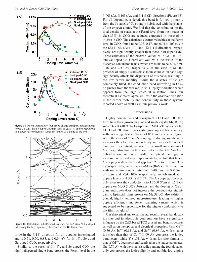
to be in the [111] direction for all dopants investigatedand is 0.51, 0.70, 0.83, and 0.94 eV for In-, Y-, Sc-, andGa-doped CdO, respectively.
Similar to the cases of In-, Y-, and Sc-doped CdO, thehighly dispersed single band crosses the Fermi level in the
[100] (∆), [110] (Λ), and [111] (Σ) directions (Figure 15).For all dopants considered, this band is formed primarilyfrom the 5s states of Cd strongly hybridized with the p statesof the oxygen atoms. We find that the contributions to thetotal density of states at the Fermi level from the s states ofGa (1.3%) in CGO are reduced compared to those of In(4.3%) in CIO. The calculated electron velocities at the Fermilevel in CGO, found to be 0.33, 0.17, and 0.04 × 10⁵ m/s inthe (∆) [100], (Λ) [110], and (Σ) [111] directions, respec-tively, are significantly smaller than those in In-doped CdO.These estimates of the electron velocities in Ga-, In-, Y-,and Sc-doped CdO correlate well with the width of thedispersed conduction bands, which are found to be 3.01, 3.91,3.36, and 2.57 eV, respectively. In the case of Sc, thepresence of empty d states close to the conduction band edgesignificantly affects the dispersion of this band, resulting inthe low carrier mobility. While the d states of Ga arecompletely filled, the conduction band narrowing in CGOoriginates from the weaker Cd 5s–O 2p hybridization whichappears from the large structural relaxation. Thus, ourtheoretical estimates agree well with the observed variationin the carrier mobility and conductivity in these systemsreported above as well as in our previous work.
Conclusions
Highly conductive and transparent CGO and CIO thinfilms have been grown on glass and single crystal MgO(100)substrates at 410 °C by low-pressure MOCVD. As-depositedCGO and CIO thin films exhibit good optical transparency,with an average transmittance of 85% in the visible region.As in the cases of Y and Sc doping, In doping significantlyincreases the electrical conductivity and widens the opticalband gap. In contrast, because of the small ionic radius ofGa, large structural relaxation reduces the Cd 5s–O 2phybridization, and as a result, the optical band gap isincreased only modestly. Experimentally, we find that In andGa doping widens the band gap from 2.85 to 3.18 and 3.08eV, respectively, via a Burstein–Moss (B–M) shift. Thin filmswith maximum conductivities of 10 400 and 20 000 S/cmon glass and MgO(100), respectively, are obtained at Indoping levels of 4.3%. and 2.6%. The Ga doping, however,only increases the conductivity to 11 500 S/cm at 1.6% Gadoping on MgO (100) substrates, and the doping of Ga onglass substrates does not increase the conductivity signifi-cantly. Epitaxial films grown on MgO(100) also exhibit abiaxial, highly textured microstructure, leading to higherdoping efficiency and fewer scattering centers, which issuggested to be responsible for the higher conductivity vsthe films on glass.25
Our theoretical and experimental results reveal that dopantion size and its electronic configuration have a significantinfluence on the CdO-based TCO crystal and band structuresas well as on the optical and electrical properties. First, Ga3+
(0.76 Å), In3+ (0.94 Å), and Sc3+ (0.89 Å), with smallerion sizes than that of Cd2+ (1.09 Å), compress the latticeparameters, while Y (1.04 Å), with an ion size similar tothat of Cd2+, does not significantly alter the lattice parameter.Ga (0.76 Å), with the smallest radius among the four dopants,only compresses the lattice slightly and exhibits low doping
Figure 14. Room temperature four-probe charge transport measurementsfor Ga-, Y-, In-, and Sc-doped CdO thin films on glass (A) and on MgO(100)(B): electrical conductivity. Lines are drawn as a guide to the eye.
Figure 15. Calculated sX-LDA band structure for 12.5 atom % Ga-dopedCdO along the high symmetry directions in the Brillouin zone.
229Chem. Mater., Vol. 20, No. 1, 2008Ga- and In-Doped CdO Thin Films

efficiency. Second, in contrast to In-doped CdO, the largestructural relaxation in CGO reduces the Cd 5s–O 2phybridization, which in turn significantly affects the disper-sion of the conduction band. The resulting small electronvelocity along with the low doping efficiency of Ga explainsthe lower mobility in CGO as compared to In-doped CdO.The experimental observations agree well with the theoreticalpredictions.
On the basis of results of the present studies, it can beseen that CdO-based TCO films generally exhibit highercarrier mobilities than do those of In2O3-, ZnO-, and SnO2-based TCO materials. This can be ascribed to the simpleCdO cubic crystal structure, the broadly dispersed free-electron-like Cd 5s-based conduction band, and the low
carrier effective masses. We find that dopant ion size has asubstantial influence on the transport and optical propertiesof CdO, specifically, on the width of the highly dispersedconduction band and its location with respect to the bandedges, which provide the necessary conditions for optimizingtransparent conducting behavior with doping.
Acknowledgment. This work was supported by the NREL(XAF5-33636-02), the NSF-MRSEC program (Grant DMR-0520513) at the Northwestern Materials Research Center, anda computer time grant from the NSF at MCA96S016. We thankDr. J. Carsello for his assistance with X-ray diffractionmeasurements.
CM702588M
230 Chem. Mater., Vol. 20, No. 1, 2008 Jin et al.