unclassified ad 409024
TRANSCRIPT
UNCLASSIFIED
AD 409024AD r,
DEFENSE DOCUMENTATION CENTERFOR
SCIENTIFIC AND TECHNICAL INFORMATION
CAMERON STATION, ALEXANDRIA, VIRGINIA
UNCLASSIFIED

NOTICE: When government or other drawings, speci-fications or other data are used for any purposeother than in connection with a definitely relatedgovernment procurement operation, the U. S.Government thereby incurs no responsibility, nor anyobligation whatsoever; and the fact that the Govern-ment may have formulated, furnished, or in any waysupplied the said drawings, specifications, or otherdata is not to be regarded by implication or other-wise as in any manner licensing the holder or anyother person or corporation, or conveying any rightsor permission to manufacture, use or sell anypatented invention that may in any way be relatedthereto.
""• Thermoelectric;Z: Thermal-Barrier Microelements
CD
--- Contract Nr. DA 36-039 SC-89212C,)C •DA Task Nr. 3A99-1 5-002-03
FINAL REPORT
1 April 1962 to 30 September 1962
Prepared for
U. S. ARMY ELECTRONICS RESEARCHAND DEVELOPMENT LABORATORY
Fort Monmouth, New Jersey
MELPAR INC
3000 ARLINGTON BOULEVARD FALLS CHURCH, VIRGINIA
NO .OTS
IASTIA AVAILABILITY NOTICE
TQualified requesters may obtain copies of this report from the Armed Services Techni-
cal Information Agency (ASTIA), Arlington Hall Station, Arlington 12, Virginia.
ASTIA release to OTS is not authorized.
THERMOELECTRIC THERMAL-BARRIER MICROELEMENTS
Contract Nr. DA 36-039 SC-89212
U.S. Army Signal Corps Technical Requirement No. SCL-7635dated 29 September 1961
DA Task Nr. 3A99-15-002-03
Final Report
1 April 1962 to 30 September 1962
The objective of this program was to develop, fabricate,and evaluate thermoelectric thermal-barrier microelements.
Prepared by
F. K. EgglestonP. A. Mullin
N. Fuschillo D D C
JULTSI I8bJ
TISIA B
TABLE OF CONTENTS
Page
LIST OF ILLUSTRATIONS 3
LIST OF TABLES 7
GLOSSARY OF SYMBOLS 9
1. PURPOSE 15
2. ABSTRACT 19
3. PUBLICATIONS, LECTURES, REPORTS AND CONFERENCES 22
4. FACTUAL DATA 23
4.1 Introduction 234.2 Theory 23
4.3 Design 444.4 Fabrication 76
4.5 Evaluation of TEB's 132
5o CONCLUSIONS 162
6. RECOMMENDATIONS 164
7. IDENTIFICATION OF KEY TECHNICAL PERSONNEL 166
8. REFERENCES 173
2

LIST OF ILLUSTRATIONS
Figure Page
1 Length of Elements Necessary To ObtainSpecific Ratio of r'/r 29
2 Heat-Pumping Performance of ThermoelectricCooling Device as Function of DimensionsFor Element Height of 0.2 cm 48
3 Heat-Pumping Capacity, Coefficient ofPerformance, and Power Input for N Thermo-electric Couples as Function of CurrentWhere N Is Number of Couples. ITh = 125 0 C,
T = 75 C, L = .2 cm, A = .01 cm 2j 66c
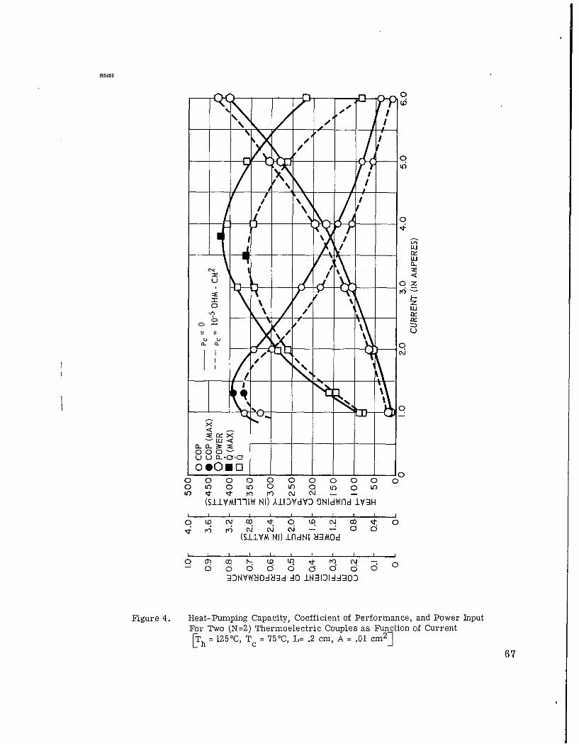
4 Heat-Pumping Capacity, Coefficient ofPerformance, and Power Input For Two (N=2)Thermoelectric Couples As Function ofCurrent [Th = 1250 C, Tc = 75 0 C, L = , cm,
A = .01 cm 2 ] 67
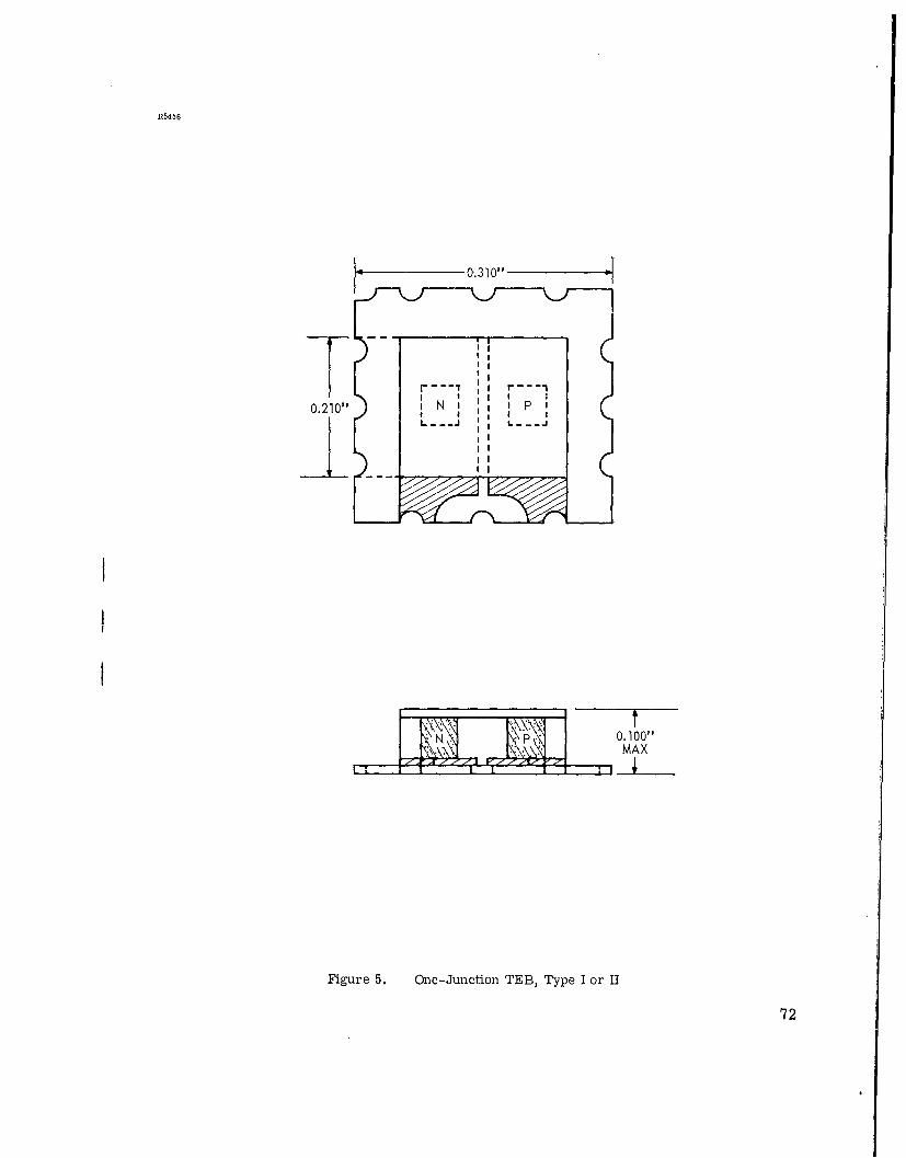
5 One-.Junction TEB, Type I or II 72
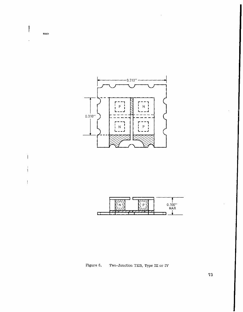
6 Two-Junction TEB, Type III or IV 73
7 Finished Single-Junction TEB, Type I or II 74
8 Finished Two-Junction TEB, Type III or IV 75
9 Flow Chart of TEB Process 78
10 Thermoelectric Material (Ingots, Pellets, andElements) 82
11 Direct Materials Involved in TEB Construction 83
12 Cutting Fixture 85
13 Semiconductor Crystal-Slicing Machine 86
3
LIST OF ILLUSTRATIONS (Continued)
14 Thermoelectric Z Meter 88
15 Resistivity Meter For Thermoelectric Materials 89
16 Seebeck Coefficient Meter 90
17 Lapping Fixture 92
18 Dicing Fixture 97
19 Resistivity Meter For Thermoelectric Elements 100
20 TEB Assembly Jig Ready For Loading 103
21 TEB Assembly Jig Showing Parts For One-JunctionDevice 105
22 TEB Assembly Jig Showing Parts For One-JunctionDevice Loaded Into Position in Jig 106
23 TEB Assembly Jig Showing Parts For Two-JunctionDevice 107
24 TEB Assembly Jig Showing Parts For Two-JunctionDevice Loaded Into Position in Jig 108
25 TEB Assembly Jig Ready For Processing 109
26 Detail Drawing of Assembly Fixture 110
27 Copper Conductors 112
28 Airbrasive Unit 115
29 Glass Encapsulation Subassembly 116
30 TEB Evaluation System 118
31 TEB Performance Evaluator 119
4
LIST OF ILLUSTRATIONS (Continued)
Figure Page
32 TEB Evaluator - Thermal Guard Model 120
33 Heat Leak-Type TEB Tester 125
34 Micromodule Substrate, Metalized 126
35 TEB Substrate Pattern (Single Junction) 127
36 TEB Substrate Pattern (Two Junction) 128
37 Hand Punch For Copper Conductor Pieces 130
38 AT vs. I Curve For Typical TEB, InitialExperimental Model (Two Junction) 133
39 AT vs. I Curve For Interim TEB Sample No. 1Supplied to USAELRDL (Two Junction) 134
40 Curve For AT(max) Determination For Interim TEB
Sample No. 1 Supplied to USAELRDL (Two Junction) 135
41 AT vs. I Curve For Interim TEB Sample No. 2Supplied to USAELRDL (Two Junction) 136
42 Performance Data, TEB, Type I 142
43 Performance Data, TEB, Type II 143
44 Performance Data, TEB, Type III 144
45 Performance Data, TEB, Type'IV 145
46 TEB, Type I-D, No. 5, Q vs. AT, With Th = 850C,Showing Typical Types I and II PerformanceWith Glass Encapsulation 146
47 TEB, Type I-C, No. 5, Q vs. AT, With Th = 850C,Showing Typical Types I and II PerformanceWithout Glass Encapsulation 147
5
LIST OF ILLUSTRATIONS (Continued)
Figure Page
48 TEB, Type III-D, No. 8, Q vs. AT, With Th = 1250C,Showing Typical Types III and IV PerformanceWith Glass Encapsulation 148
49 TEB, Type III-C, No. 8, Q vs. AT, With Th = 125°C,Showing Typical Types III and IV PerformanceWithout Glass Encapsulation 149
50 TEB, Type I-C, Average AT vs. I Curves ForQ=5 mw 152
51 TEB, Type I-D, Average AT vs. I Curves ForQ = 5 mw 153
52 TEB, Type II-C, Average AT vs. I Curves ForQ = 50 mw 154
53 TEB, Type II-D, Average AT vs. I Curves ForQ = 50 mw 155
54 TEB, Type III-C, Average AT vs. I Curves ForQ = 10 mw 156
55 TEB, Type III-D, Average AT vs. I Curves ForQ = 10 mw 157
56 TEB, Type IV-C, Average AT vs. I Curves ForQ = 50 mw 158
57 TEB, Type IV-D, Average AT vs. I Curves ForQ = 50 mw 159
6
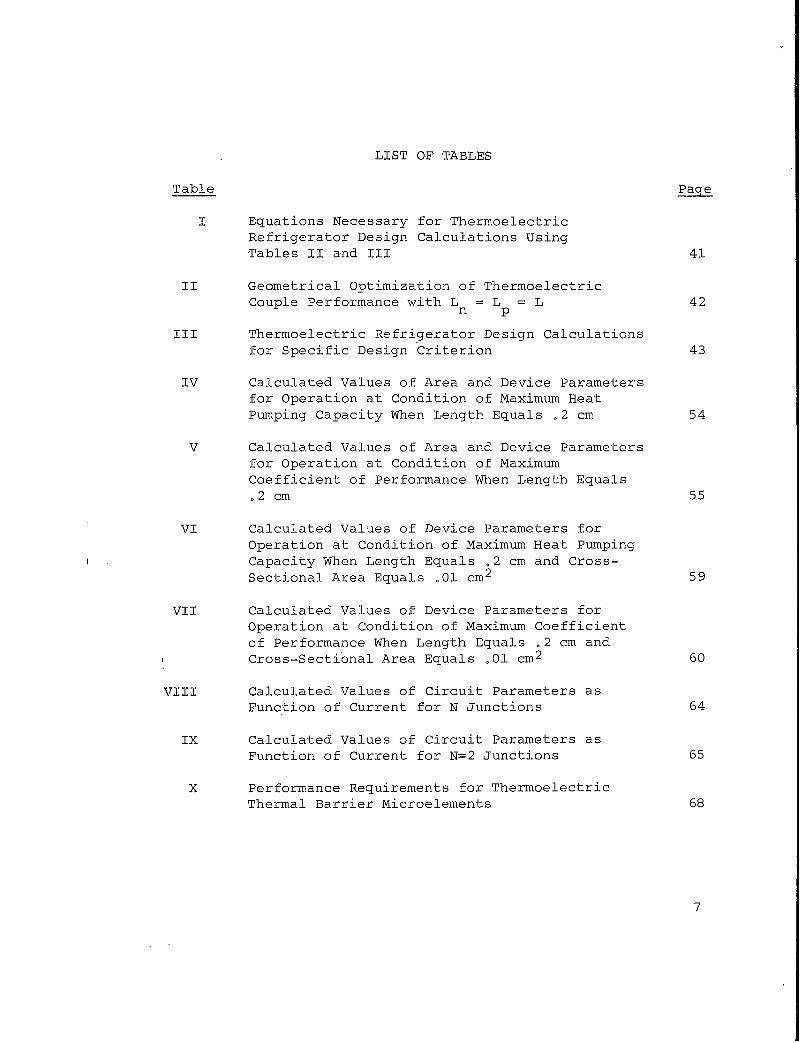
LIST OF TABLES
Table Page
I Equations Necessary for ThermoelectricRefrigerator Design Calculations UsingTables iI and IIi 41
II Geometrical. Optimization of ThermoelectricCouple Performance with L = L = L 42n p
III Thermoelectric Refrigerator Design Calculationsfor Specific Design Criterion 43
IV Calculated Values of Area and Device Parametersfor Operation at Condition of Maximum HeatPumping Capacity When Length Equals .2 cm 54
V Calculated Values of Area and Device Parametersfor Operation at Condition of MaximumCoefficient of Performance When Length Equals.2 cm 55
VI Calculated Values of Device Parameters forOperation at Condition of Maximum Heat PumpingCapacity When Length Equals .2 cm and Cross-Sectional Area Equals .01 cm2 59
VII Calculated Values of Device Parameters forOperation at Condition of Maximum Coefficientof Performance When Length Equals .2 cm andCross-Sectional Area Equals .01 cm2 60
VIII Calculated Values of Circuit Parameters asFunction of Current for N Junctions 64
IX Calculated Values of Circuit Parameters asFunction of Current for N=2 Junctions 65
X Performance Requirements for ThermoelectricThermal Barrier Microelements 68
7
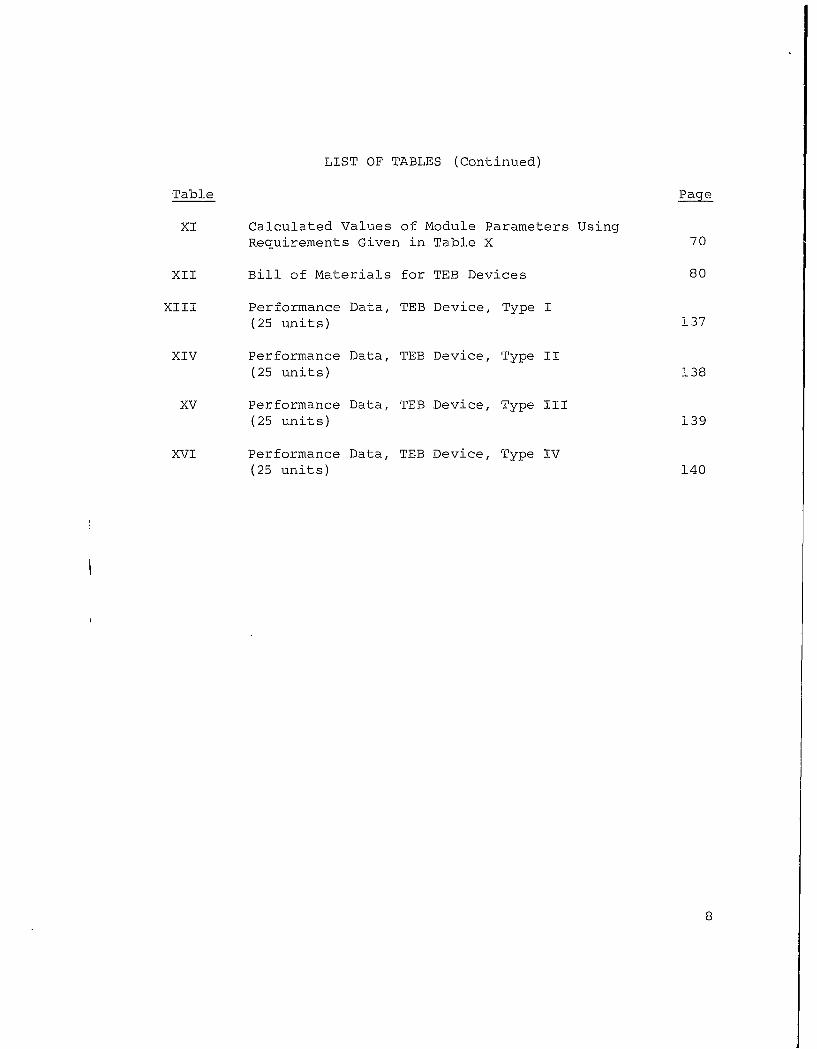
LIST OF TABLES (Continued)
Table Page
XI Calculated Values of Module Parameters UsingRequirements Given in Table X 70
XII Bill of Materials for TEB Devices 80
XIII Performance Data, TEB Device, Type I(25 units) 137
XIV Performance Data, TEB Device, Type II(25 units) 138
XV Performance Data, TEB Device, Type III(25 units) 139
XVI Performance Data, TEB Device, Type IV(25 units) 140
8
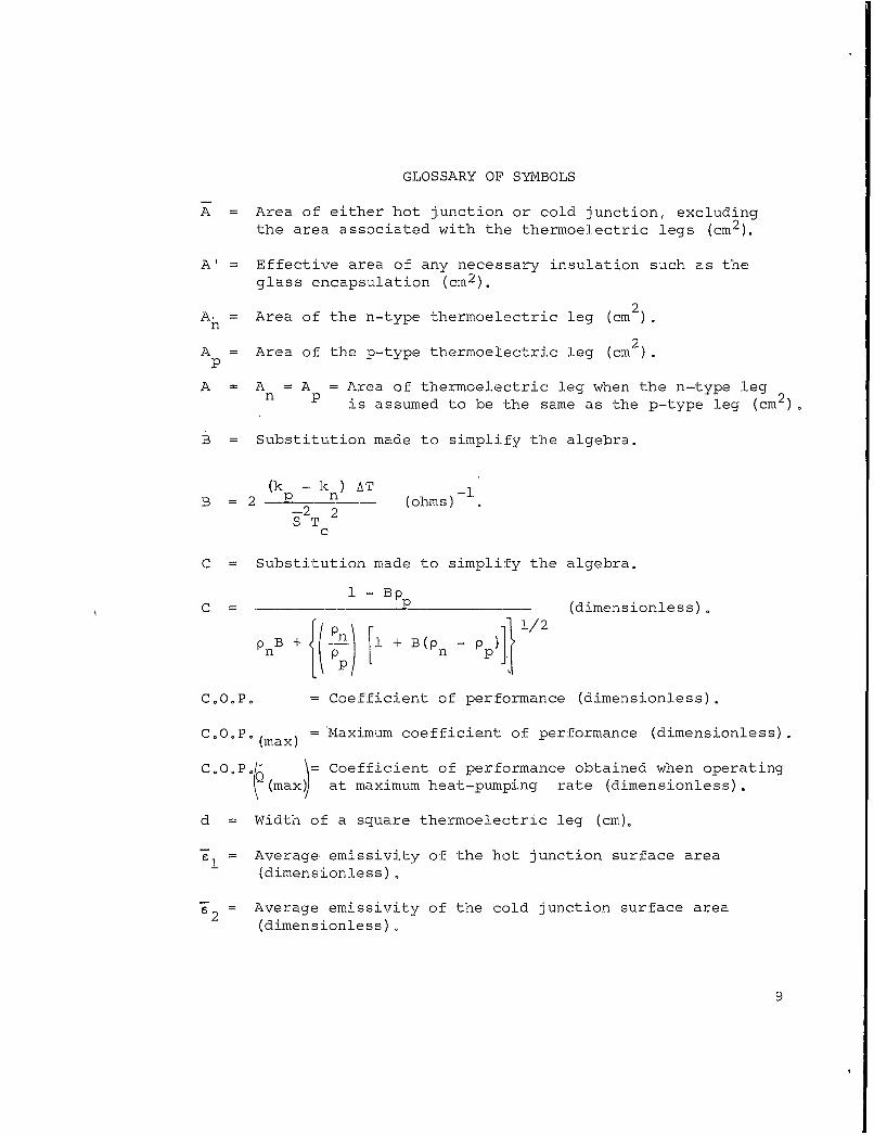
GLOSSARY OF SYMBOLS
A = Area of either hot junction or cold junction, excludingthe area associated with the thermoelectric legs (cm2 ).
A' = Effective area of any necessary insulation such as theglass encapsulation (cm 2 ).
A, = Area of the n-type thermoelectric leg (cm2n
A = Area of the p-type thermoelectric leg (cm 2).
A A = A = Area of thermoelectric leg when the n-type legn P is assumed to be the same as the p-type leg (cm
B = Substitution made to simplify the algebra.
(k - k )AT -lB = 2 P n (ohms)--2 2
STc
C = Substitution made to simplify the algebra.
1 -B
C = 1 Bp_ P -(dimensionless).
PnB + n [1 + B(Pn - pp)] 1/2
CO.oPo = Coefficient of performance (dimensionless).
CO0.P° (max) Maximum coefficient of performance (dimensionless).
C 0oPo( = Coefficient of performance obtained when operating. (max)) at maximum heat-pumping rate (dimensionless).
d = Width of a square thermoelectric leg (cm),
"FI = Average emissivity of the hot junction surface area(dimensionless),
62 = Average emissivity of the cold junction surface area(dimensionless),
9
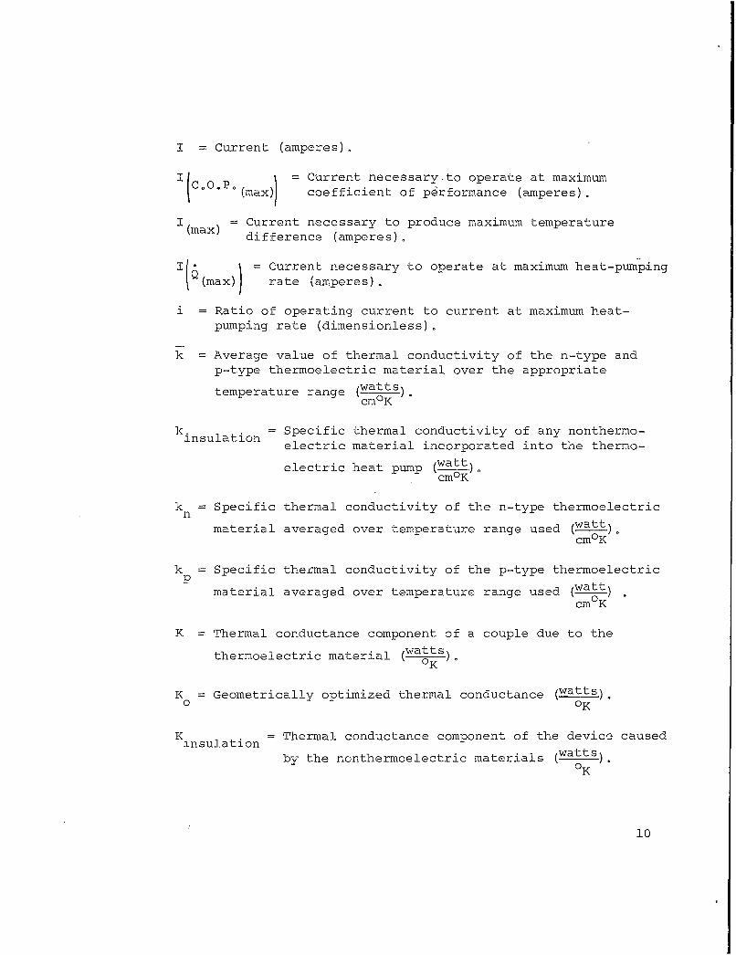
I = Current (amperes).
= Current necessary to operate at maximum
Co0Po (max)) coefficient of performance (amperes).
I max) = Current necessary to produce maximum temperaturedifference (amperes),
Current necessary to operate at maximum heat-pumpingI(max)) rate (amperes).
i = Ratio of operating current to current at maximum heat-pumping rate (dimensionless).
k = Average value of thermal conductivity of the n-type andp-type thermoelectric material over the appropriate
temperature range (watts).cmoK
kinsulation = Specific thermal conductivity of any nonthermo-electric material incorporated into the thermo-
electric heat pump (watt),cmOK
k = Specific thermal conductivity of the n-type thermoelectric
material averaged over temperature range used (watt).cmOK
k = Specific thermal conductivity of the p-type thermoelectric
material averaged over temperature range used (watt)cm°K
* = Thermal conductance component of a couple due to the
thermoelectric material (watts)
K = Geometrically optimized thermal conductance (watts).0 OK
K insulation = Thermal conductance component of the devicc caused
by the nonthermoelectric materials (watts).0 K
10
K = Thermal conductance component of the device caused byr radiation through the nonthermoelectric part of the
device (watts).OK
K' = Total thermal conductance of a thermoelectric device
(watts)OK-
K' K + Kinsulation + Kr-
"K(electron) = Thermal conductance of thermoelectric material dueto charge carriers (watts).
OK
"K(lattice) = Thermal conductance of the thermoelectric materialdue to phonon and photon energy transfers through
the lattice (watts).oK
L = Length of the thermoelectric leg when the n-type leg isassumed to be the same length as that of the p-type leg (cm).
L = Length of the n-type thermoelectric leg (cm).n
L = Length of the p-type thermoelectric leg (cm).p
m -r Substitution made to simplify differentiation ofS equation defining coefficient of performance (OK).
M = Dimensionless quantity used to describe the operatingparameters of a thermoelectric couple operating at maximum
coefficient of performance. (M =\ 1 + ZT)
N = Number of two-leg thermoelectric couples placed in serieselectrically,
n(subscript) = Denotes that a particular parameter is associatedwith the n-type thermoelectric material.
p(subscript) = Denotes that a particular parameter is associatedwith the p-type thermoelectric material.
P = Power input to the thermoelectric couple (watts).0
11
P I l = Power input when operating at maximum coefficientoCoO.Po(max)ý of performance (watts)°.
P) = Power input when operating at maximum heat-pumping'+\(max)ý rate (watts).
Q = Heat-pumping capacity of the system (watts).
Q(max) = Maximum heat-pumping capacity (watts).
= Heat-pumping capacity when the system is operating6 (max) at maximum coefficient of performance (watts).
Qt = Total heat load of the system including all heat losses(watts).
r = Radiation heat loss (watts).r
Qinsulation = Heat loss by conduction through any nonthermo-electric material (watts).
R = Electrical resistance of a single thermoelectric leg (ohms).
R = Contact resistance of a single solder connection (ohms).c
R' = Contact resistance associated with both ends of a thermo-c electric leg (ohms),
r = Electrical resistance component of a couple due to thermo-electric material (ohms),
r = Contact resistance associated with a two-legthermoelectric couple (ohms),
r' = Total electrical resistance of a two-leg thermo-electric couple (ohms),
r'= r + rc
r 0 Geometrically optimized resistance (ohms).0
12
S = (S - S ) Combined Seebeck coefficient of a thermo-" P electric couple made up of an n-type and a
p-type leg averaged over temperature range
used (microvolts).oK
S = Seebeck coefficient of the n-type thermoelectric legn
averaged over temperature range used (microvolts)OK
S = Seebeck coefficient of the p-type thermoelectric legaveraged over temperature range used (microvolts).
OK
T = Temperature (OK).
T = Temperature of the cold junction (OK).c
Th = Temperature of the hot junction (OK).
TL = Temperature of the thermal load (°C).
TTG = Temperature of thermal guard radiation shield (°C).
T= 1/2 (Th + T c) (OK).
AT = Temperature difference between the hot and cold junctions(OK).
AT =T -Tc.
AT = Maximum temperature difference between the hot andcold junctions (oK).
V = Seebeck voltage across the couple (volts).0
= Voltage when operating at maximum coefficientV C.O'p.(max) of performance (volts).
V = Voltage input to the thermoelectric couple (volts).
= Voltage when operating at maximum heat-pumpingV 6(max)) rate (volts).
13
Z = Therioelectric figure of merit (°K)-
Z = Geometrically optimized figure of merit ( K)-1
0
Z' = Thermoelectric figure of merit which includes contact
resistance (OK)-i
Z" = Thermoelectric figure of merit which includes contactresistance and nonthermoelectric material thermal
conductance (°K)-i
= Average value of the electrical resistivity of the n-typeand p-type thermoelectric material over the appropriatetemperature range (ohm-cm)-
Pn = Electrical resistivity of the n-type thermoelectricmaterial averaged over temperature range used (ohm-cm).
pp = Electrical resistivity of the p-type thermoelectricmaterial averaged over temperature range used (ohm-cm).
Pc = Contact resistivity associated with both the n-type andp-type thermoelectric material (ohm-cm2 )o
S= Ratio of thermoelectric leg area to its length (cm).
7= A/Lo
14
1. PURPOSE
1.1 Objective
The objective of this contract was to develop, fabricate,
and evaluate thermoelectric cooling devices which would be
suitable for direct incorporation into Army micromodules as
special microelements having the purpose of protecting heat-
sensitive circuit elements. These devices, called Thermoelectric
Thermal Barrier Microelements (TEB's), would be located between
microelements bearing heat-sensitive and heat-generating circuit'
elements. The performance requirements for these devices are
given by Signal Corps Technical Requirement No. SCL-7635 and
are summarized in table X.
1.2 Work Division
The work was divided into the following tasks and phases:
TASK A
Phase 1. THEORETICAL ANALYSIS
Part A. Design (including thermoelectricmaterial considerations).
(1) Optimization of design.
Part B. Materials (other than thermo-electric).
Phase 2. MATERIALS ACQUISITION
Part A. Thermoelectric materialsoptimized for operation at72.5 0 C and 100 0 C.
Part B. Micromodule substrates.
Part C. Insulating and structuralmember (based on Task A,Phase 1B).
Part D. Silicone and epoxy resins(standard types used in micro-module program).
15
Part E. Materials and supplies requiredfor processing and testing devices.
TASK B
Phase 1. EXPERIMENTAL
Part A. Construct several devices ofeach type (from designs ofTask A, Phase IA).
Phase 2. EVALUATIONS EQUIPMENT
Part A. Construct necessary evaluationequipment.
(1) Material meter.
(2) Device evaluator.
Phase 3. EVALUATION OF EXPERIMENTAL MODELS
Part A. Evaluate all test models inpreliminary test setup todetermine whether performanceis as expected.
TASK C
Phase 1. PRODUCTION OF DEVICES REQUIRED FOR DELIVERY
Part A. Construct at least 35 of eachtype, allowing for failures anddestructive testing.
(1) Make jigs and fixturesrequired for production.
(2) Prepare materials forassembly.
Phase 2. EVALUATION OF DEVELOPMENT MODELS
Part A. Evaluate all devices fordelivery, using equipmentconstructed in Task B, Phase2A(2).
Phase 3. FINAL REPORT
Part A. Prepare Final Report.
16
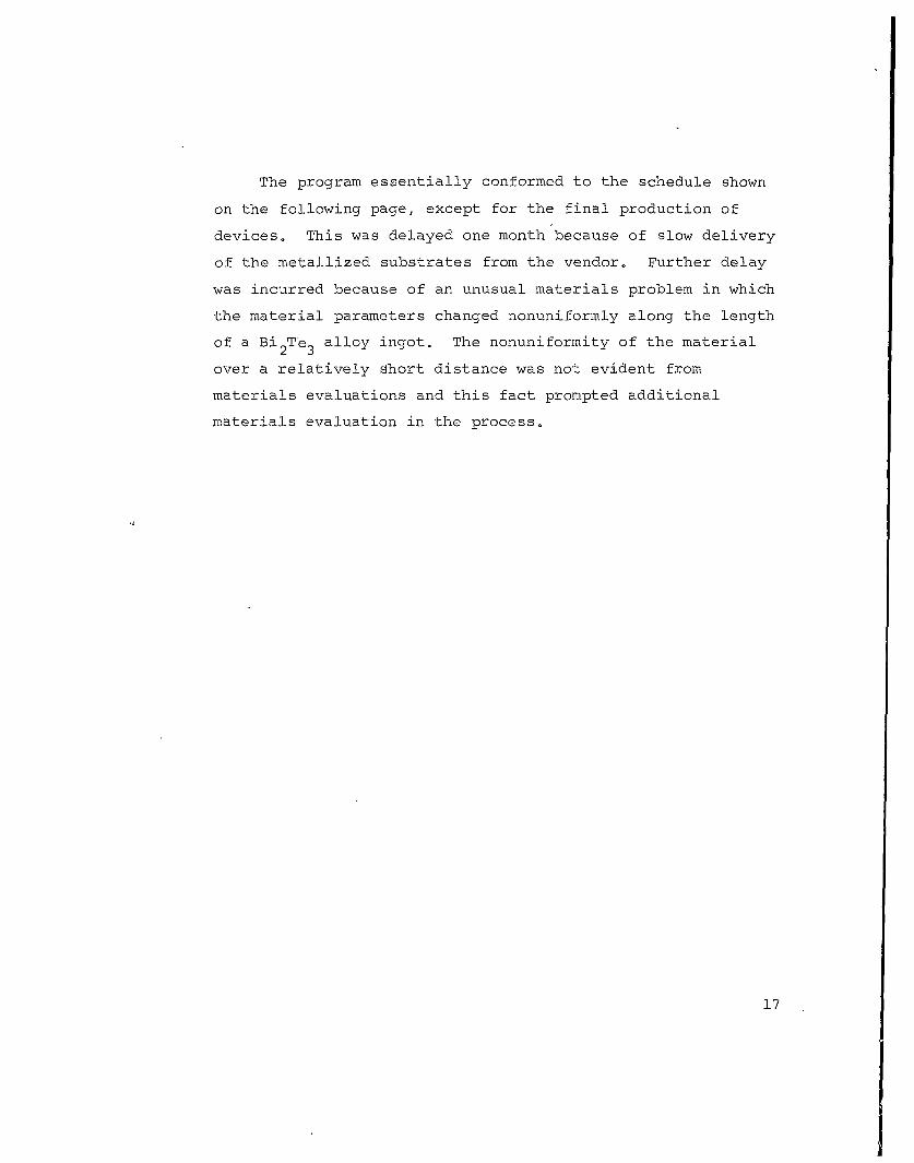
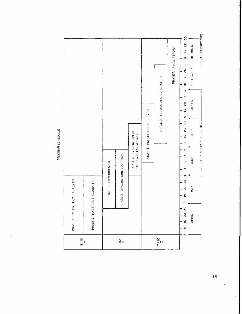
The program essentially conformed to the schedule shown
on the following page, except for the final production of
devices, This was delayed one month because of slow delivery
of the metallized substrates from the vendor. Further delay
was incurred because of an unusual materials problem in which
the material parameters changed nonuniformly along the length
of a Bi2 Te3 alloy ingot. The nonuniformity of the material
over a relatively short distance was not evident from
materials evaluations and this fact prompted additional
materials evaluation in the process.
17
to D
0 U., o LU0 0 o
ILUmc u
000<z
z -F-
cj. LU
z V) H UJo -< I--
0 LUJ
< U o
LU -uH
LLN 00~ :3J
LLU
LL Lo 0 ) uu
0z < i :LU 0u
ov m LU< 0 I0v) w v
(D LU Z0 N LUIU'
>H LU LO1 H wzo Z n LUJ < U
<U m N L LU
LU LU V
Hj :D OD ' L
z >LUO LU UL
LI _ zi< LU
0 LU 0-0<~
L~CLLI) -i <
InI
EL L
-j~
< < < HLU LU
LU 0
2. ABSTRACT
2. 1 1a ect ive
The objective of this contract was to design, fabricate,
and evaluate micromodule thermoelectric cooling devices which
would be suitable for direct incorporation into Army micro-
modules as special microelements having the purpose of pro-
tecting heat-sensitive circuit elements. These devices, called
Thermoelectric Thermal Barrier Microelements (TEB's) would be
located between microelement wafers supporting heat-sensitive
and heat-generating circuit elements.
Selective temperature control, as a new circuit design
parameter, holds the promise of increasing the reliability
and performance of electronic packaging of the high density
required to reduce the space and weight requirements associated
with defense electronic systems.
2.2 Design
The design theory related to Thermoelectric Thermal
Barrier (TEB) microelements is developed and all equations
used in the design are derived and discussed, Design criteria
are established and the anticipated performance of the designs
adopted to meet type !, II, 1I, and IV conditions (SCL-7635)
is calculated.
2.3 Fabrication
An account is given of the characteristics of the thermo-
electric material used and the process steps involved in the.
construction of type I to iV TEB devices, including a description
of the test and performance evaluation methods developed for
the devices. The normal precautions to be taken in the handling
and manufacture of the TEB devices are also given.
19
2.4 Results
The results of performance evaluations of the prototype
devices are presented for Th = 125 0 C and thermal loads of 50,
100, and 200 mw (see figure 39). These results were obtained
by measuring T as a function of current. The test data underc
type I to IV conditions is presented on each of the four batches
of 25 units designed to meet type I to IV conditions. One
hundred operational units were supplied to USAELRDL which had
been tested to meet the required specifications.
Dataare presented from more complete tests on six single-
junction and six double-junction devices. These include AT
and T vs. I curves for various heat loads, maximum temperaturec
difference under zero applied heat load, and temperature
difference vs. heat load for various constant currents.
The results of the evaluations are discussed in relation
to the design theory. An effective device figure of merit of
2.5 x 10⁻³ 3 -I1 without encapsulation is deduced from the
experimental results at the specified type I to IV operating
points. The difference between this and a measured materials
figure of merit of 2.8 x 10⁻³ "(idl is shown to be attributable
to the independently calculated values of radiation exchange
between Th and Tc and of contact resistance. A device figure
of merit of Z" = 2.1 x 10- 3oKrl was calculated when the
magnitude of thermal conduction through the glass encapsulation
was taken into account. This theoretical value agreed well
with that deduced from the experimental results.
2.5 Conclusions
Several conclusions were drawn from a consideration of the
design, fabrication, and device evaluation part of this work.
20
The principal conclusion is that the devices designed and
constructed easily meet the required specifications of USAELRDL
Technical Requirement No. SCL-7635o The excess heat-pumping
capacity built into these devices will enable them to meet
higher thermal loads, under type I to IV temperature-difference
conditions, than specified in SCL-7635o
2.6 Recommendations
Although the devices developed in the present contract
easily meet the specified type I - IV operational requirements,
several worthwhile improvements can be made. These are:
a. Improvements of the present device configurations.
b. Improvement in the configurational design which is
possible with improved materials fabrication and p - n junction
contacting technology.
c. Additional cooling concepts,
21
3. PUBLICATIONS, LECTURES, REPORTS, AND CONFERENCES
3.1 Publications
None.
3.2 Lectures
None.
3.3 Reports
Five Monthly Letter Reports were prepared as a part of
this program. These were as follows:
a. First Monthly Letter Report, by N. Fuschillo, dated
2 May 1962, for the period 1 April through 30 April 1962o
b. Second Monthly Letter Report, by N. Fuschillo, dated
1 June 1962, for the period 1 May through 31 May 1962,
c. Third Monthly Letter Report, by N, Fuschillo, dated
2 July 1962, for the period 1 June through 30. June 1962.
d. Fourth Monthly Letter Report, by N, Fuschillo, dated
2 August 1962, for the period 1 July through 31 July 1962.
e. Fifth Monthly Letter Report, by N. Fuschillo, dated
31 August 1962, for the period 1 August through 31 August 1962.
3.4 Conferences
Four conferences between Signal Corps and Melpar personnel
were held to discuss the progress of work during the period
1 April to 30 September 1962. Two meetings were held at USAELRDL
and two were held at Melpar at approximately equally spaced
intervals.
The authors acknowledge the cooperation and valuable
guidance contributed to this program by Dr. H. J. Dagenhart and
Mr. H. C. Frankel of USAERDL.
22
4. FACTUAL DATA
4.1 Introduction
This part of the r2port contains a discussion of the
design, fabrication, and evaluation of Thermoelectric Thermal
Barrier (TEB) microelement heat pumps. Early in the dis-
cussion, all of the relevant equations used in thermoelectric
refrigerators are derived and discussed (subparagraph 4.2).
This general treatment of thermoelectric cooling device theory
is then applied to design of TEB microelement heat pumps (sub-
paragraph 4.3).
Subparagraph (4.4), Fabrication, contains a detailed
description of all process steps as well as related information.
The testirig and evaluation of the thermoelectric material and
the completed devices are considered part of the TEB process
and are d~scribed in paragraph 4.
The results of the device evaluations for type I, II, III,
and IV devices (see table X), together with a discussion of
the results, are given in subparagraph 4.5.
4.2 Theory
A theoretical analysis of thermoelectric heat-pumping
systems is presented below. The final result is presented in
tables I-II, which contain the equations used in thermoelectric
design. These tables have been useful in the design of thermo-
electric systems, Refer to Glossary of Symbols for terminology
and meaning of symbols used in the following derivations.
23
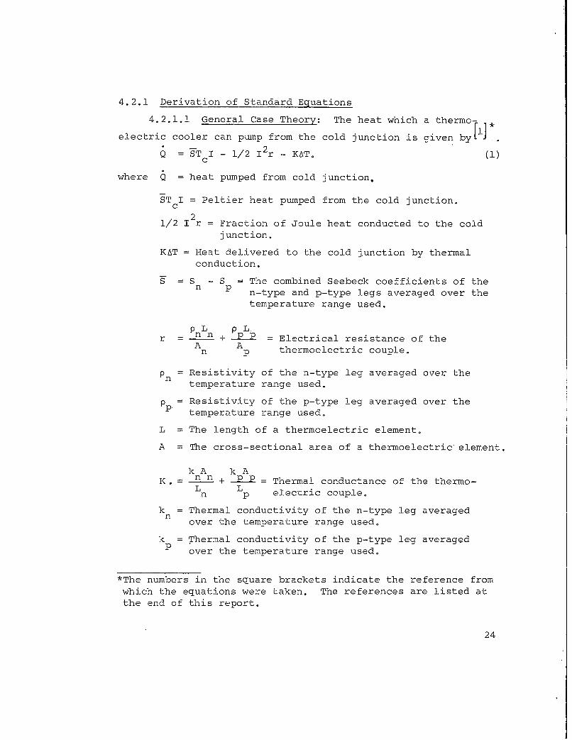
4.2.1 Derivation of Standard Equations
4.2.1.1 General Case Theory: The heat which a thermo-
electric cooler can pump from the cold junction is given byW.
Q = ST I - 1/2 1 2 r - KATo (1)c
where Q = heat pumped from cold junction,
ST I = Peltier heat pumped from the cold junction.c2
1/2 I r = Fraction of Joule heat conducted to the coldjunction.
KAT Heat delivered to the cold junction by thermalconduction.
S S - S = The combined Seebeck coefficients of then P n-type and p-type legs averaged over the
temperature range used.
r PnLn + pPLP = Electrical resistance of theA A thermoelectric couple.
Pn = Resistivity of the n-type leg averaged over thetemperature range used.
pp Resistivity of the p-type leg averaged over thetemperature range used.
L = The length of a thermoelectric element.
A = The cross-sectional area of a thermoelectric element.
kA k AK. = n n + P P = Thermal conductance of the thermo-
L L electric couple.
k = Thermal conductivity of the n-type leg averagedover the temperature range used.
k = Thermal conductivity of the p-type leg averagedpover the temperature range used.
*The numbers in the square brackets indicate the reference fromwhich the equations were taken. The references are listed atthe end of this report.
24
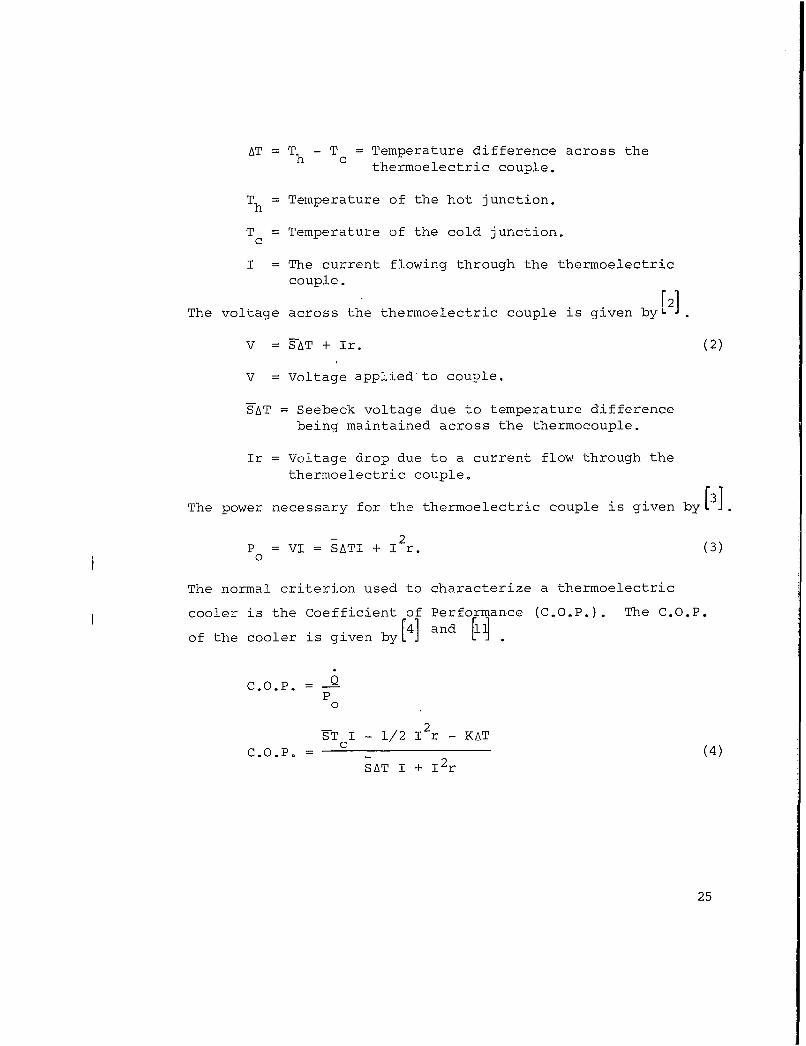
AT = Th - Tc = Temperature difference across thethermoelectric couple.
Th = Temperature of the hot junction.
T = Temperature of the cold junction.c
I = The current flowing through the thermoelectriccouple.
The voltage across the thermoelectric couple is given by[2]
V = TAT + Ir. (2)
V = Voltage applied to couple,
SAT = Seebeck voltage due to temperature differencebeing maintained across the thermocouple.
Ir = Voltage drop due to a current flow through thethermoelectric couple.
The power necessary for the thermoelectric couple is given by[3].
- 2P = VI = SATI + I r. (3)0
The normal criterion used to characterize a thermoelectric
cooler is the Coefficient of Performance (CoO.P.). The C.O.P.
of the cooler is given by[4] and [1ý
C.O.P. QP0
2ST I - 1/2 I r - KAT
Co.P= (4)SAT I + 12r
25
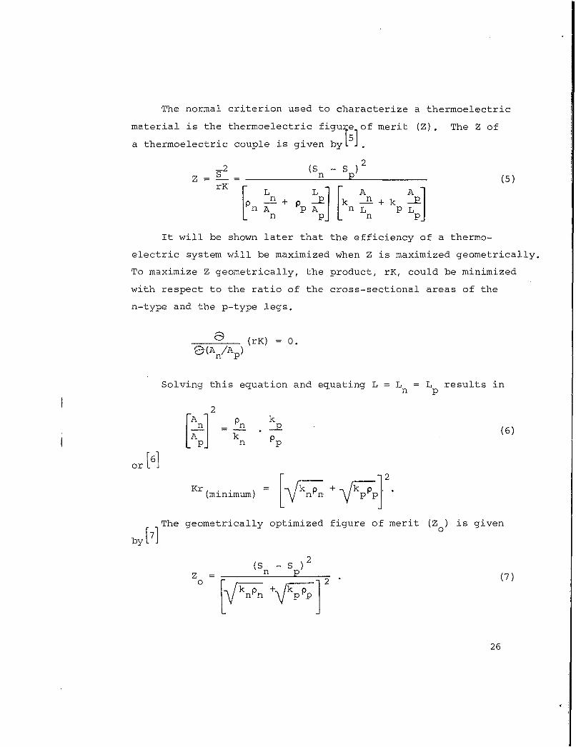
The normal criterion used to characterize a thermoelectric
material is the thermoelectric figure of merit (Z). The Z of
a thermoelectric couple is given by1.
-2 (S2
Z _ - n p(5)rK
__n + __ [knA + kn A 'p n L pn pn
It will be shown later that the efficiency of a thermo-
electric system will be maximized when Z is maximized geometrically.
To maximize Z geometrically, the product, rK, could be minimized
with respect to the ratio of the cross-sectional areas of the
n-type and the p-type legs.
a - (rK) = 0.a(A n/A )
Solving this equation and equating L = L = L results inn p
2
[] - _(6)
[An P k pp
or [61
Kr (minimum) n L+ kP]2
The geometrically optimized figure of merit (Z ) is given
0 2(s -s
Z n= . (7)
26

Another common criterion used to characterize the thermo-
electric cooler is the maximum temperature difference that can
be maintained across it. By rearranging equation (1), we have[8]ST I - 1/2 12r -
AT = c (8)K
It follows from equation (8) that, all other conditions
remaining constant, AT will be increased as
Q -, 0
and will be maximum when Q = 0,
This, then, allows equation (8) to become
.2S T I - 1/2 1 r
AT Q c K (9)
To maximize ATe we must let1[9]
S(AT) = 0
0 = S T - Ir
S T
max r
where I is the current which will produce the maximummax
temperature difference.
Substituting this value of I back into equation (9)
results in[101 max
_2 2 2S T ZT
AT = c _ c (10)(max) 2rK 2
27
From equation (10), it can be seen that from the measure-
ments of two temperatures under the condition that they
represent the maximum temperature difference maintainable by
a thermoelectric couple, the effective figure of merit of the
material in the couple can be determined directly.
So far, the discussion has been restricted to design
criterions for ideal couples, i.e., ones which do not have
contact resistances or thermal losses associated with them.
The problem of contact resistance has hindered the development
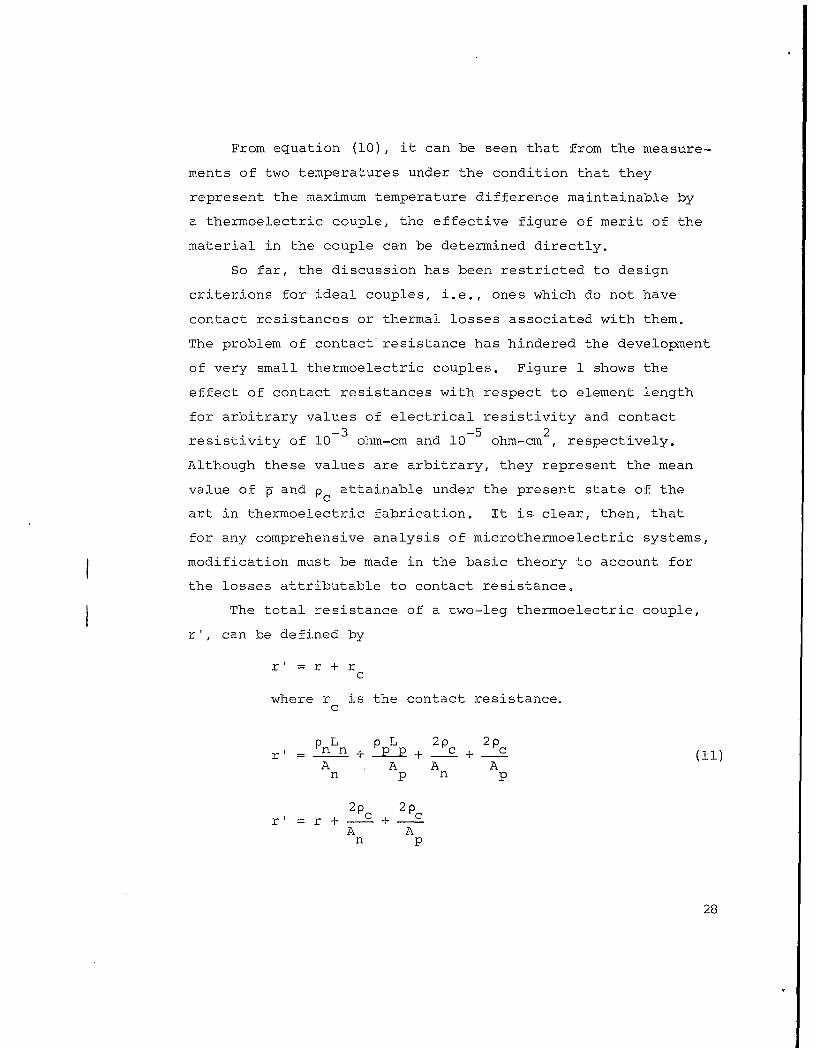
of very small thermoelectric couples. Figure 1 shows the
effect of contact resistances with respect to element length
for arbitrary values of electrical resistivity and contact
-3 -5 2resistivity of 10 ohm-cm and 10 ohm-cm , respectively.
Although these values are arbitrary, they represent the mean
value of p and p c attainable under the present state of the
art in thermoelectric fabrication. It is clear, then, that
for any comprehensive analysis of microthermoelectric systems,
modification must be made in the basic theory to account for
the losses attributable to contact resistance.
The total resistance of a two-leg thermoelectric couple,
r', can be defined by
r' = r + rc
where r is the contact resistance.c
PnLn p 2 Pc 2cr' - + pL c +-c + (11)
A A A An p n p
r' r + 2pc + 2pc
A An p
28
R4662 L +01010
___ _ _ ___L 2Pý F1jP Lrl
SEE REFERENCE [36]
I--zLU-Iu-i 10-1U-0
zLU-i
1o20-2
1.0 1.2 1.4 1.6 1.8 2.0 2.2 2.4
RATIO OF r' r
Figure 1. Length of Elements Necessary To Obtain Specific Ratio of r' /r
29
where Pc = value of contact resistivity and for
most cases, where A = A = A
n p
r' = r+ 4pc (12)A
A new figure of merit can be defined to take into account
the contact resistance
2(Sn - S )
Z i n
r'K
If Pn = and L n L = L, then Z' can be written as
Z - z z (13)+r c +2 pc
r
The total thermal conductance of a thermoelectric couple,
K', can be defined by
K' =K + K(insulation) + K (14)
where K =K +K (5(lattice) (electron) (15)
A new figure of merit is defined to take into account both
contact resistance and thermal conductivity.
z" = Pn (16)r'K'
Z" = Z (17)
+ i + r (insulation)r3K
: 30
It should be noted here that in all the equations given
throughout the remainder of the design theory, r' can be used
instead of r, K' can be used instead of K, and Z' and Z" are
interchangeable with Z or Z0
4.2.1.2 Case of Maximum Coefficient of Performance:
Equation (4) gave the definition of the loefficient of per-
formance of a thermoelectric cooler as [
-- 2rST I - 1/2 I r - KAT
C.O.P. c (4)
7AT I + I r
Ir
Let m =- (18)
and substitute into equation (4). The C.O.P. can then be
written as H2 KA
mT - 1/2 m KrATc -2
C.O.P =2 (19)mAT + m
Equation (19) shows that the C.O.P. can be optimized by
adjusting m, which is a function of I from equation (18), and
by adjusting the product, Kr. Because C.O.P. is positive, it
is maximized by minimizing the product, Kr. Assume that the
length of the p-type leg is the same as that of the n-type leg
(L = L = L). Then, to minimize the product, Kr, letn p
a (r) = 0S(An/Ap)
The area ratio under this condition is given by equation
(6).
31

This results in
r L Pn (20)ro A f( k 1/2 p
and
K = __. k k n + k (21)o L ppkn} pP
where r and K are the values of resistance and thermal0 0
conductance geometrically optimized for maximum CO.,Po Putting
these values of r and K into equation (5) results in the0 0
geometrically optimized thermoelectric figure of merit as
given by equation (7) on page 26 of this report.
Putting these values of r and K into equation (4) results0 0
in
C.O S--T I - 1/2 12 r 0- K 0AT (2C .o o = c o 0 ( 2 2 )
SAT I +1 2r°
To optimize CoOoPo with respect to the current, let
B(C.OoPo) = 0.
32

Solving this gives [14]
= r SAT (23)(M - 1)
where M = l (24)
and 7 = 1/2 (Th 4, Tc)O (25)
Puttinrlg this value of I back into equation (22) gives [15]
T T
CoOoP( 0 max) AT (26)
Equation (26) shows that the CoOoPo (max) is made up of two
qT
components• •--" which is the CoOoPo of a Carnot refrigerator,AT
and which can be thought of as representing theM+l 1
degree to which the thermoelect.r,.c couple approaches an ideal
Carnot refrigerator,
To obtain the amount of heat pumped under the condition
of maximum Coefficient of Perform.ance, the value of I from
equation (231 is substi.tuted back into equation (1). This
results in
=_ S2AT [c AT 1 ] (27)Q(CoOoPoImax,) r LM-l 2(M - 1)2 zj
This same value of current substituted into equations (2)
and (3) gives for the voltage [16] and power input [177 for
CoO oPo Imax)
33
SATM (28)VýC-O - P- (max)ý M - 1°
2 MPCO ' (max)) ) 0(2
4.2.1.3 Case of Maximum Heat-Pumping Rate: Equation (1)
gives the equation for the amount of heat pumped by a thermo-
electric couple as[l]
2Q = ST I - 1/2 I r - KATo (1)
To maximize Q with respect to current, let
aQ= 0.
This results in a value of current such that[181
ST
Q(~a) r c (30)
Substituting this valu~e of current back into equation (1)
results in[191
c T-2T 2
Q(max) 2r KAT (31)
The geometrical optimization will be given now. As before,
let L = L = L. The usual objective in designing for maximumn p
heat-pumping rate is to obtain a given capacity with a minimum
size or minimum weight, or to minimize the amount of thermo-
electric material required. These objectives require that the
total cross-sectional area, AT = An + A p, be as small as possible.
34

Therefore, the term which should be maximized is -QA
This is done by letting T
S(Ap) AT=p Ti•
The result is given by [201
A PnB + (sB (p+B P -1/
-L- =P / L (32)Ap (1 - Bpp)
where [21]
2(k -kn)ATB -
•2T 2c
This gives
r- + p (33)Aro Pn B + (Pný ý1 + B (')Pn "Pp) l/ 2
i and
pnB + 1 + B (Pn -p
A PpJ
K =-2 k n+ k (34)0 L n( - B pp) P
where r and K are now the values of the resistance and thermal0 0
conductance of the thermoelectric couple geometrically optimized
for maximum, heat pumping.
35
The figure of merit for this case is given by
(S - s 2
Z 0 n p (35)
P nkn + ppkp P + pkC++ - C
where
1 - Bp
PnB + (Th [1 + B (Pn- Pp)
The values substituted back into equation (31) give[22]
Q'(max) L 2 Pn+ 2p -AT (Akn +Ak)I (36)
[23]
The voltage for Q(max) is given by[23]
V (max)) = S2Th(37)
and the input power is given byi24l
S-f2 TcTh
Po(• (max)) r0 (38)
From equations (4) and (30), the COo.Po under the
condition of maximum heat pumping rate is given by
1 2 ATZc•
C (OoPo Q(max)) 2 (1 + •-)AT(
T
36
4.2.1.4 The Thermoelectric Refrigerator Equations in Terms
of AT, In paragraph 4.2.1.1, equation (10) defined a(- max)'quantity [!0]
2AT (max) = 1/2 ZT c (10)
Equation (10) states that the maximum temperature that can be
developed across a thermoelectric couple is dependent only on
the thermoelectric figure of merit and the temperature of the
cold junction of the thermocouple. It is interesting to note
that all of the equations derived previously for 6(max)'
Q(C.O.P.a)) ,CO'P () and C'O'P'(6(max)) can be written
to a first approximation in terms of AT(a
The term for Q(max) as given in equation (31) becomes,
after using the substitution from equation (10),1251
i F AT 1S(max) = KAT (max) AT (max) (40)
Equation (39) becomes[26]
C..P. ( ) = 1/2 1 - AT(m )( AT (41)
Equation (27) becomes [27]
Q(~.P~) KAT (1 - AT A ) (42)QCOoPo(max) AT(max3
37
while equation (26) becomes [28]
1 ATAT
C*0TP (max) (43)C'0P(max) 2( AT + AT)AT/(max) T c
Using this notation, two more equations evolve, namely:[29,30]
ATA Q (max) (44)SC..Po(max) AT(max)
and
CO a) • AT C.O.p. (max) (45)C.O.P. 6(max)ý AT (max)(mx
Comparing equations (44) and (45) leads to the following
conclusion:
x Q((max) x Q (max) (m)C.O.P. m (46)-(a(ma(x)
This is significant because it appears that the choice of
operating at either maximum C.0.P. or maximum Q has no effect
on the product of C.O.P. x Q.
The general case equations can also be given in terms of
AT (max)' and IQ6 (max) where I1 (max)= the current which gives
maximum heat pumping 8]
ST'( (max)) r 30)
38

Equation (1) becomes [31]
Q= KAT (2i - i2 _ AT A) (47)S(ma) AT(max)
and equation (4) becomes[32]
2- 2 AT2i - i 2 A
C.O.P - AT (max) (48)2(i2 + AT i)
Tc
where[33]
i I (49)
Q (max))
I = the current used for any operation.
4.2.1.5 The Concept of Effective Thermal Conductance:
Equations (1), (27), and (31) give the expressions for Q,
i . and Q (max) in terms of the basic parameters.
These equations can be rewritten in terms of an effective thermal
conductance by using the following substitution:
(Sn - S p)2
Zr
The advantage of using this form is that a good insight
as to what is happening physically can be seen from the equations,
and these equations lend themselves well to calculations.
39
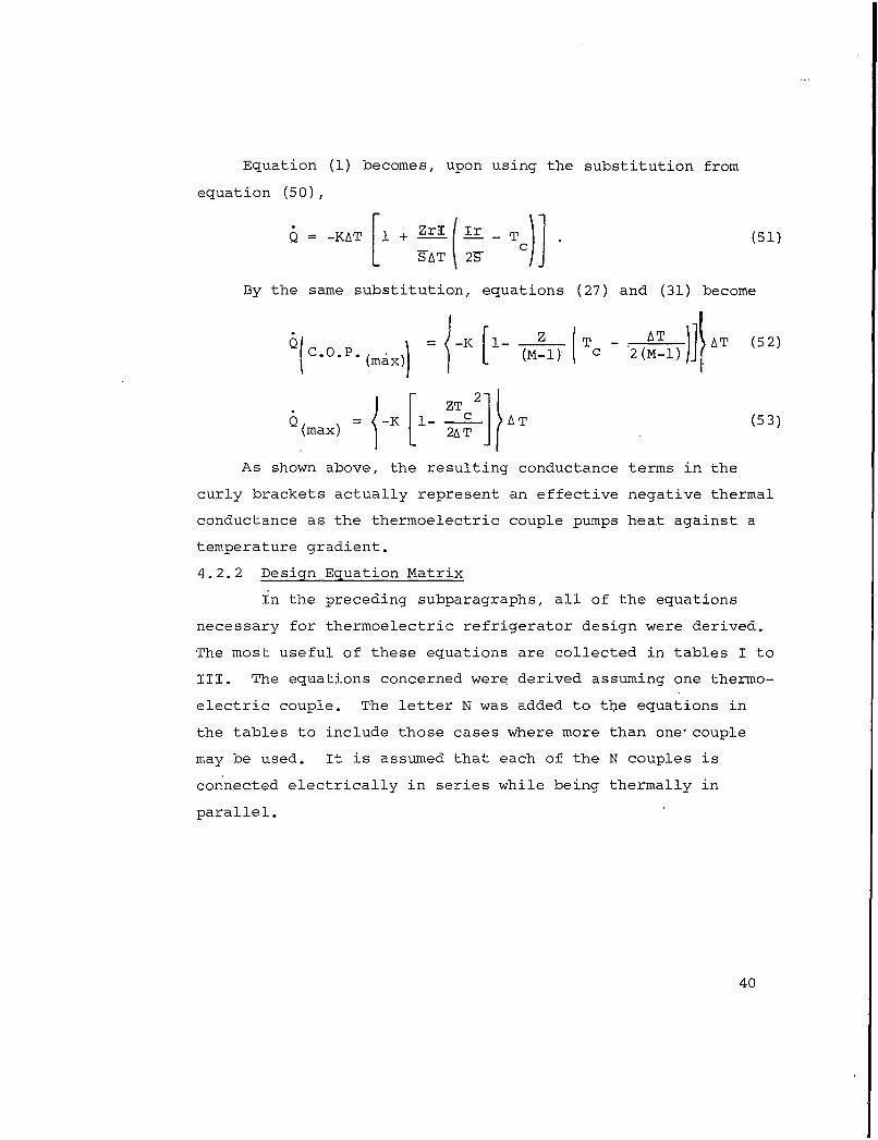
Equation (1) becomes, upon using the substitution from
equation (50),
-KAT i + ZrI TA (51)
By the same substitution, equations (27) and (31) become
Q!C.O.P.(m)) -K [1- Z T AT AT (52)(m Xl(M-1) c 2 (M-1)
(max) = [ 1 c AT (53)(max)2A T
As shown above, the resulting conductance terms in the
curly brackets actually represent an effective negative thermal
conductance as the thermoelectric couple pumps heat against a
temperature gradient.
4.2.2 Design Equation Matrix
in the preceding subparagraphs, all of the equations
necessary for thermoelectric refrigerator design were derived.
The most useful of these equations are collected in tables I to
III. The equations concerned were derived assuming one thermo-
electric couple. The letter N was added to the equations in
the tables to include those cases where more than one couple
may be used. It is assumed that each of the N couples is
connected electrically in series while being thermally in
parallel.
40
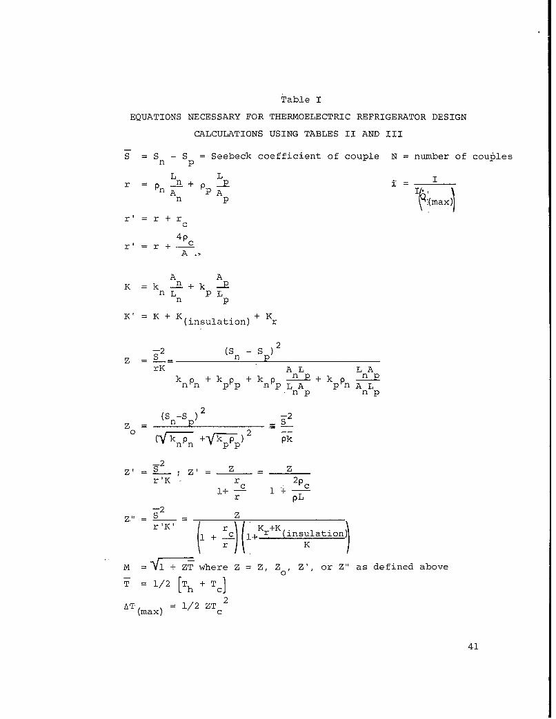
Table I
EQUATIONS NECESSARY FOR THERMOELECTRIC REFRIGERATOR DESIGN
CALCULATIONS USING TABLES II AND III
S = S - S = Seebeck coefficient of couple N = number of couplesn p
L L I=n A PA A
n p !.(max)
r= r + r c4 p
A .
A AK =k n + kn L P L
n p
K = K + K(insulation) + Kr
z - - (S n - p)
rK A L LAknPn +k p +k np + n pppp knPpLA Ppn L
n p n p
Z(S n-S p ) 2--2z - s__0 (knn + k-pp) 2 --
pkn~n p p
-' 2Z-I = ZI z - z
r'K r 2pl+_c 1 •2c
r pL-2
Z" - S _ Z
r'K' (1 + 1_)(Kr+I(ins lation)
r KM = + ZT where Z = Z, Z, Z', or Z" as defined above
T = 1/2 ETh + TIc
AT(max) = 1/2 ZTc 2
41
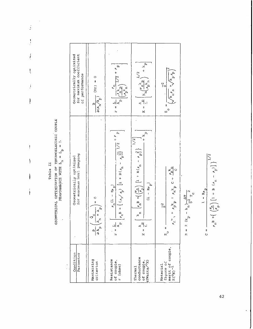
~4-H) H
OnA-1 04 94J J K1 -
0~U 0
i H 0
Wr ) 04
44 0
N0
1210D0
04
HH
04Io Ný VI
H P4
H E-. + l~
H 0 4uO c0 04
0I OE- cQ Q PI- UH) H 1 " E- E
0 w~ K- 0 + ~0 p
a)0 04 -4
00
HO 0 04
ON 0 0) 0 H+j
Hr 4J 04+ 1) 0)
Nr ý r CO+:1 u1 a) 4
1211 m 0q0Z - 14404c2 N 0- 01 O0 ) 144J0 , (
a)- H)0N ý 4 4P4H4,J) - )r o Jtýý 0
42W o~ 42
HIN.H a I I4 0 (
aC) 9
1,4<00 *(b pH E) U<l
-z HV + <~ -- (
H 1C -.ý (N
H (N E,4 <1 H1 E 1 HI HIw
-Z Zi HIlN I- HzII 11 *II -11 11 It 11 11 11
HU) 0
oN 0
U HE4H HHý 04(
U4 4 , O
0. C) H NC
0 N Hq HEH
o H -z'~
1N It (
a) U
H -
H
__ H N Ný
W4 ( N NU 1 Np t 114F-lH HH-<l1
N
HS H
(N
N~~ C13* 0
H -H 0)1 NH (N a) z (N (N 1 4-0 4J Hqu0 jPa
O) 044 C: HH " > 4 CuHv -H 0 0 ~ - C 41 rH C- 0J a) d 40-
p 4 1 r' 4a ,C 0
,) -H o0 ) p014 4 0.' -H a) aC)0 C) 011 C)1-C.)C 0 a) L-I 4 04 *Q 0) C) C4J 0 C) a)0
U0 d 41 a) NC 1d)t4-4 04 rd - *H 0 X 44-PC) 14 0 IN, 0)4 0.? 0 X
43
4.3 Design
4.3.1 Qualitative Design Analysis
Taking into account the special requirements of Thermo-
electric Thermal Barrier Microelements and the level of per-
formance desired, the optimum device design involves designing
for minimum current and the use of the maximum allowable element
height.
The requirements given in SCL-7635 are quite explicit in
defining the problem and the specifications which the TEB micro-
elements must meet. The requirements and specifications are
reviewed in the following subparagraphs.
4.3.1.1 Thermoelectric Material: The thermoelectric
material's figure of merit is required to be not less than
about 3 x 10- 3 (°oKl. Bismuth telluride alloys are the only
materials currently available with this figure of merit.
Thermoelectric materials of this type are normally maximized
for operation at room temperature. The figure of merit for
Bi-Sb-Te-Se alloys decreases with temperature above 200 C. At
125 C, the figure of merit for a p-type material can decrease
by as much as 30% from the value at 20 0 C, while n-type material
only suffers a decrease of the order of a few percent over the
same temperature range. Because the average operating tempera-
tures of the thermoelectric thermal barrier heat pumps are 100 0C
and 72.5 0 C in the two environments under consideration, it is
obviously desirable to optimize the figure of merit of the
thermoelectric material in this temperature range.
4.3.1.2 Size: Regarding the specification of size and
space available for TEB microelements (0.210" x 0.210" x 0.100"),-
this is more than adequate. The maximum height specification
44
is influential in determining the maximum allowable cross-sectional
area of the TEB microelement legs (because the operating current
range is also specified). Using the design criterion of minimum
current and recognizing the importance of minimum contact
resistance fraction, it is desirable to have the maximum length
for the thermoelectric elements. The maximum height of the TEB
microelement assemblies should then be 0.1 of an inch.
4.3.1.3 Electric Power: A low driving current is specifi-
cally desired for the TEB microelements (less than three amperes).
This can be achieved by choosing a proper geometry factor, A/L,
where A = cross-sectional area of a thermoelectric junction leg
and L = length of a thermoelectric junction leg. Because the
area which gives the desired current range will be small and
maximum length is defined by the height requirements, the
feasibility of a current of less than three amperes is easily
determined. It is possible for the required current to be less
than one ampere.
4.3.1.4 Fabrication and Operational Stresses: The stresses
encountered by TEB microelements during fabrication into micro-
modules are not considered harmful to the thermoelectric portions
of the TEB once it has been assembled into a unit. Small-thermo-
electric assemblies can successfully withstand the stresses
associated with curing epoxy resins at 125 0 C. Ultrasonic
cleaning techniques have been successfully used for cleaning
thermoelectric devices after they had been assembled.
Regarding operational stresses, the effects of the operating
temperature range, storage, and temperature cycling with
accompanying thermal expansions and contractions should not cause
any severe problems. Unpublished temperature-cycling experiments
by one of the authors on other cooling devices have shown
45
excellent stability under both operating and storage conditions
after several thousand hours.
4.3.1.5 Design for Minimum Current: In designing TEB heat
pumps as specified in SCL-7635, there are three principal design
modes:
a. Design for minimum current or maximum operational
voltage.
b. Design for minimum element height (which affects TEB
height).
c. Design for optimum compromise between minimum current
and minimum element height.
The design for minimum current is best suited to the
required specifications. Minimum current generally implies a
high coefficient of performance and a high operational voltage
(if the geometry factor is right). The maximum current specifi-
cation of three amperes sets the geometry factor range because
this defines the resistance. The height specification for the
TEB sets the element length because it is desirable for the
element resistance to be as great as possible. This is desirable
for two reasons:
a. So that the contact resistance fraction can be as small
as possible.
b. So that the current can be as low as possible.
Knowing the approximate geometry factor and element length, the
cross-sectional area is easily found.
The consideration of contact resistance is important because,
if the contact resistance fraction of the total device resistance
becomes appreciable, the effective Z of the device is reduced.
Assuming a contact resistivity of approximately 1 x 10⁻⁵ ohm-
centimeter2 and using an area of 0.01 cm 2, this gives for- one leg:
46
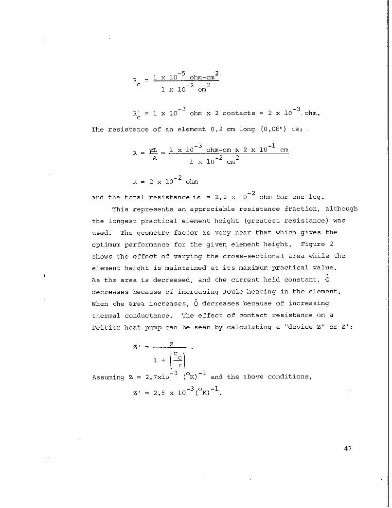
R 1 x 10⁻⁵ ohm-cm2
C 1 x 10⁻² cm2
R'= 1 x 10 ohm x 2 contacts = 2 x 10 ohm.c
The resistance of an element 0.2 cm long (0.08") is:
R = 1 x 10⁻³ ohm-cm x 2 x c0- mA 1 x 10⁻² cm2
R =2 x 10⁻² ohm
-2and the total resistance is = 2.2 x 10 ohm for one leg.
This represents an appreciable resistance fraction, although
the longest practical element height (greatest resistance) was
used. The geometry factor is very near that which gives the
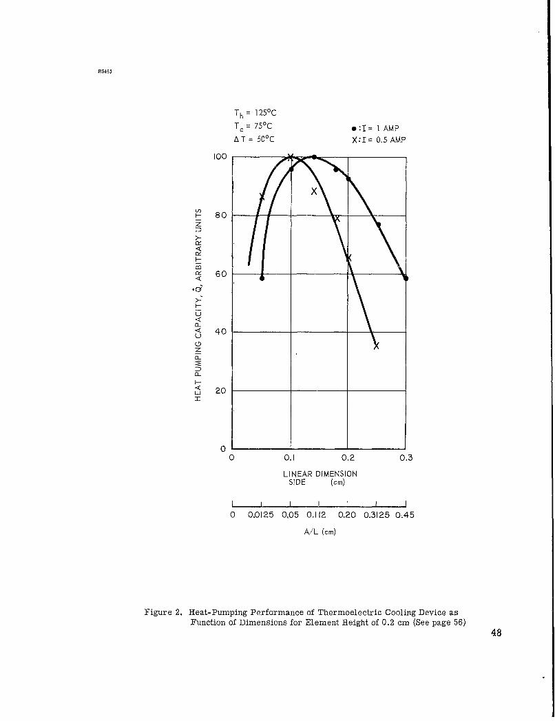
optimum performance for the given element height. Figure 2
shows the effect of varying the cross-sectional area while the
element height is maintained at its maximum practical value.
As the area is decreased, and the current held constant, Q
decreases because of increasing Joule heating in the element.
When the area increases, Q decreases because of increasing
thermal conductance. The effect of contact resistance on a
Peltier heat pump can be seen by calculating a "device Z" or Z':
=I z
Assuming Z = 2.7xl-3 ( K)- and the above conditions,
-3 o -1Z' = 2.5 x 10 (°K)
47
R5453
Th = 125°C
Tc= 75 0C *:I= 1 AMP
AT= 50 0C X:I= 0.5 AMP
100
x- 0z
>-
LU 20. 0
I-
50_< 40u
z
< 20
0
0 0.1 0.2 0.3
LINEAR DIMENSIONSIDE (cm)
S I I I I I I
0 0.0125 0,05 0.112 0.20 0.3125 0.45
A/L (cm)
Figure 2. Heat-Pumping Performance of Thermoelectric Cooling Device asFunction of Dimensions for Element Height of 0.2 cm (See page 56)
48

4.3.1.6 Design For Minimum TEB Height: From the consider-
ations of contact resistance and heat pump performance vs.
dimensional considerations shown in figure 2, this design mode
can definitely be ruled out.
4.3.1.7 Design For Optimum Compromise Between Minimum
Current and Minimum Element Height: This design mode suggests
a compromise between minimum I and minimum height. This is
ruled out on the same grounds as above because it requires
further shortening of the heat pump elements which would result
in even smaller effective device Z.
4.3.1.8 Summary: We are left with one design mode, the
design for minimum current or highest operational voltage using
the maximum practical element height. It is desirabie to have
as high a TEB voltage as possible to match more closely the
power supplies commonly used in Signal Corps equipment; These
considerations are discussed quantitatively in the following
subparagraph.
4.3.2 Design Calculations
In the following design calculations we have considered
the desirable thermocouple height to be limited to 0.2 cm by
the maximum height of the TEB microelement specified in SCL-7635.
The design problem then becomes one of reducing the area of
cross section of the thermoelectric legs of the TEB to a minimum
to minimize the current required to achieve type IV operating.
condition, which is the most demanding of the four conditions
of device operation. This minimum cross-sectional area is
calculated below and is impractically small from the standpoint
of fabrication. Calculations are then performed for a cross-
sectional area of .01 cm2 , which was considered the practical
minimum because of the time scale of the contract.
49
All of the equations necessary to design any thermoelectric
heat pump have been reviewed in subparagraph 4.2 and are
summarized in tables I, II, and III. The utilization of these
equations requires a precise knowledge of the n-type and the
p-type material parameters. To facilitate the calculations in
this subparagraph it will be assumed that the average values
of the material parameters for the n-type material are the same
as those for the p-type material. These average parameters are
assumed to be as follows:
S- InI + = 440 microvoltsS n] + Sp deg Kelvin
Pn= p = = 10 ohm-cm
= 10-5 ohm-cm2
k k = W = 1.76 x 10- 2 wattsn p cm-deg Kelvin
With these average values of the material parameters, all
of the device's operating parameters will be calculated.
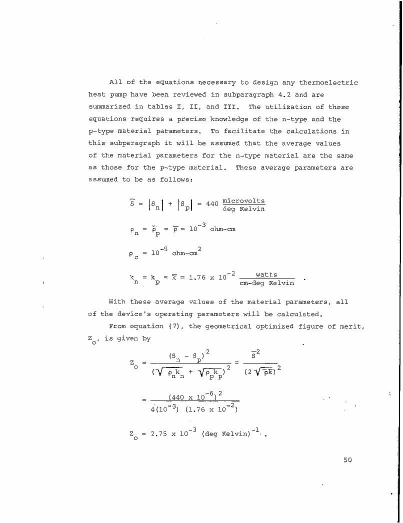
From equation (7), the geometrical optimized figure of merit,
Zo, is given by
2 -- 2
Z(San - s p) _ = s(S 2~oPnkn + _jrQ k) (2 P-k )2
n 'p 2
- (440 x l0-6) 2
4(.0-3) (1.76 x 10⁻²)
-3 -iZ = 2.75 x 10 (deg Kelvin)
0
50
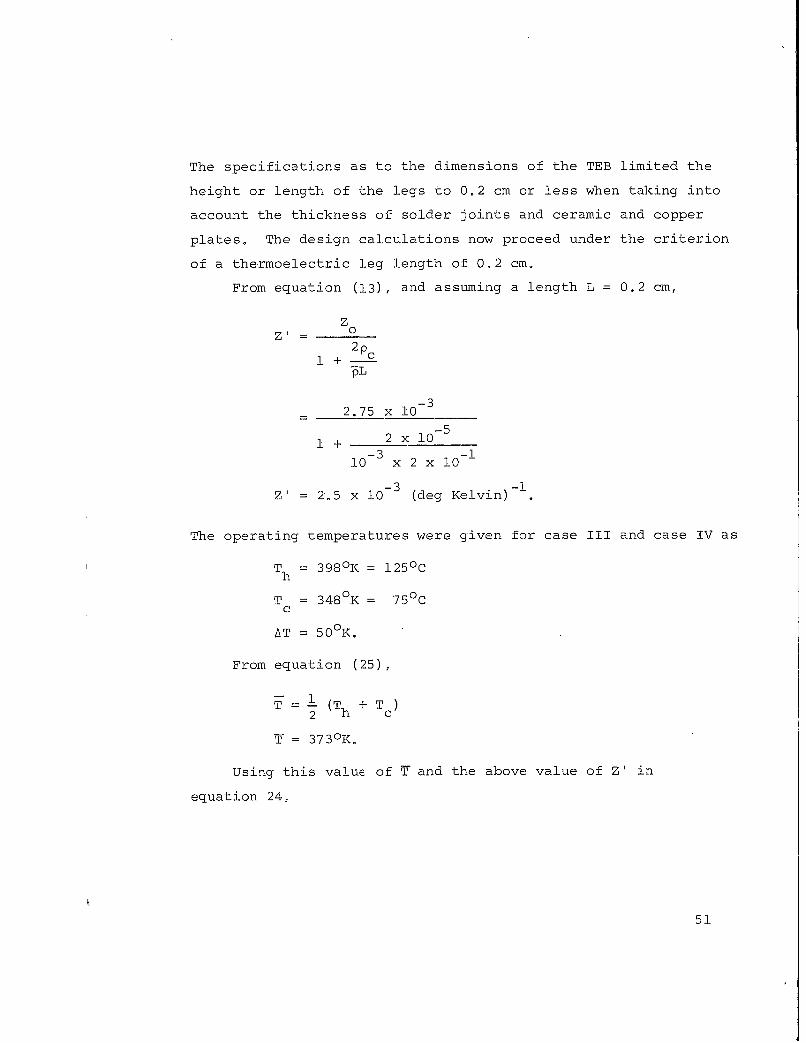
The specifications as to the dimensions of the TEB limited the
height or length of the legs to 0.2 cm or less when taking into
account the thickness of solder joints and ceramic and copper
plates. The design calculations now proceed under the criterion
of a thermoelectric leg length of 0.2 cm.
From equation (13), and assuming a length L = 0.2 cm,
z=i 0
1+ ýL
2.75 x 10³
+ 2 x 10⁵
i0-3 x 2 x 10-1
-3 -lZ' = 2.5 x 10 (deg Kelvin)
The operating temperatures were given for case III and case IV as
Th = 398 0 K = 125 0C
T = 348 0 K = 750 Cc
AT = 50°K.
From equation (25),
2 (Th + Tc)
= 373 0K.
Using this value of T and the above value of Z' in
equation 24,
51
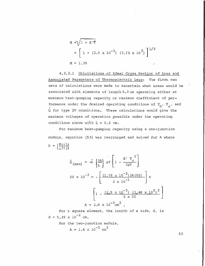
M =V± + Z'T
= [ 1 + (2.5 x l0-) (3.73 x 10²)
M = 1.39
4.3.2.1 Calculations of Ideal Cross Section of Area and
Associated Parameters of Thermoelectric Legs: The first two
sets of calculations were made to ascertain what areas would be
associated with elements of length 0..2 cm operating either at
maximum heat-pumping capacity or maximum coefficient of per-
formance under the desired operating conditions of Th, T c, and
Q for type IV conditions. These calculations would give the
maximum voltages of operation possible under the operating
conditions above wish L = 0.2 cm.
For maximum heat-pumping capacity using a one-junction
module, equation (53) was rearranged and solved for A where
kZ 2
(max) = -k AT [ Z1 T 1
50 x 10 - ( 1.76 x 10⁻² )2A(50) x
L 2 x 10⁻¹- 3322
(2.5 x 10- ) (3.48 x 10²)2-22 x 50
A = 2.8 x 10 cm
For a square element, the length of a side, d, is
d =5.29 x 10 cm.
For the two-junction module,
A = 1.4 x 10 cm 5
52
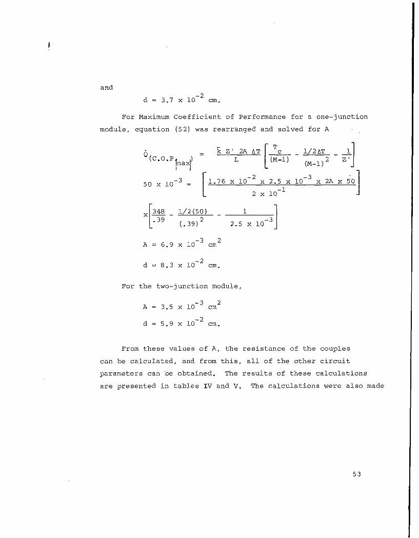
and
d = 3.7 x i02 cm.
For Maximum Coefficient of Performance for a one-junction
module, equation (52) was rearranged and solved for A
6 - Z' 2A AT Tc - /2AT 1501 3 = 1.76-x 102 -3
Q(c..oP L) (M-1) 2 zjýmaxI (M- 1 )
50 x 10-3= 1.76 x 10- 2 x 2.5 x 10-3 x 2A x 50
2 x 10⁻¹
xL348 _ 1/2(50)( 13)_- 3-9 (.39) 22.5 x 10- 3
A = 6.9 x 10- cm2
d = 8.3 x 10 cm.
For the two-junction module,
A= 3.5 x10 cm
d = 5.9 x 10⁻² cm.
From these values of A, the resistance of the couples
can be calculated, and from this, all of the other circuit
parameters can be obtained. The results of these calculations
are presented in tables IV and V. The calculations were also made
53
Table IV
CALCULATED VALUES OF AREA AND DEVICE PARAMETERS FOR OPERATIONAT CONDITION OF MAXIMUM HEAT PUMPING CAPACITYý6 (max))
WHEN THE LENGTH EQUALS o2 cm (Th=1 2 5 0 C, Tc=75 0 C)
One junction (two legs) Two junctions (four legs)
-5 2 -5 2PC= 0 PCo10-5hm-cm PC = 0 Pc=10 ohm-cm
Q(watts) 5 x 10⁻² 5 x 10⁻² 5 x 10⁻² 5 x 10⁻²
A (cm ) 2,4 x 10⁻³ 2.8 x 10⁻³ 1.2 x 10⁻³ 1.4 x 10⁻³
d (cm) .049 .053 .035 .037
r (ohm) .16 .14 °66 .57
r' (ohm) .16 .16 o66 o63
I (amp) .93 °97 .47 .49
C.OoP° .31 .29 .31 o29
V (volts) .18 .17 .35 .35
P (watts) 1.6 x 10⁻¹ 1o7 x 10 1.6 x 10⁻¹ 1.7 x 10- 1
54
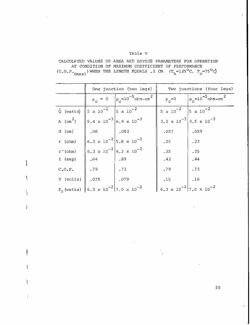
Table V
CALCULATED VALUES OF AREA AND DEVICE PARAMETERS FOR OPERATIONAT CONDITION OF MAXIMUM COEFFICIENT OF PERFORMANCE
(C.O.P. (max))WHEN THE LENGTH EQUALS .2 CM (Th=125 0 C, Tc=750 C)
One junction (two legs) Two Junctions (four legs)
P= 0 =10-5 ohm-cm2 P=0 P=10-5 ohm-cm2
S(watts) 5 x 10⁻² 5 x 10⁻² 5 x 10⁻² 5 x 10⁻²
A (cm2 6.4 x 10⁻³ 6.9 x 10⁻³ 3.2 x 10⁻³ 3.5 x 10⁻³
d (cm) .08 .083 .057 .059
r (ohm) 6.3 x 10⁻² 5.8 x 10- 2 .25 .23
r'(ohm) 6.3 x 10⁻² 6.3 x 10⁻² .25 .25
I (amp) .84 .89 .42 .44
C.O.P. .79 .72 .79 .72
V (volts) .075 .079 .15 .16
P (watts) 6.3 x 102 x 10-2 7.0 x 10⁻²
55
for Pc = 0 to show what effect contact resistance has on the
device parameters. This data is also included in the tables.
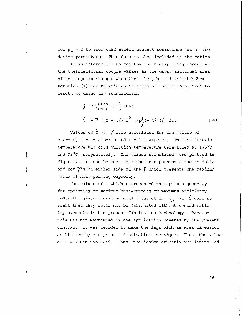
It is interesting to see how the heat-pumping capacity of
the thermoelectric couple varies as the cross-sectional area
of the legs is changed when their length is fixed at 0.2 cm.
Equation (1) can be written in terms of the ratio of area to
length by using the substitution
- _ area _A (cm)length L
Q S T I - 1/2 12 (2•k)- 1 I (() AT. (54)
Values of Q vs. T were calculated for two values of
current, I = .5 amperes and I = 1.0 amperes. The hot junction
temperature and cold junction temperature were fixed at 1250C
and 75 0C, respectively. The values calculated were plotted in
figure 2. It can be seen that the heat-pumping capacity falls
off for T(s on either side of the ( which presents the maximum
value of heat-pumping capacity.
The values of d which represented the optimum geometry
for operating at maximum heat-pumLping or maximum efficiency
under the given operating conditions of Th, Tc, and Q were so
small that they could not be fabricated without considerable
improvements in the present fabrication technology. Because
this was not warranted by the application covered by the present
contract, it was decided to make the legs with an area dimension
as limited by our present fabrication technique. Thus, the value
of d = 0.1cm was used. Thus, the design criteria are determined
56
by dimensional limitations imposed by the contract specifications
in regard to length of the elements and fabrication limitations
in respect to the cross-sectional area. Therefore, the calcu-
lations for Q(max)" CO.Po (max)' and associated I, V, and P for
a module made upý of legs which were0. 2 cm x0.1 cm x0.l cm in
dimensions are now presented.
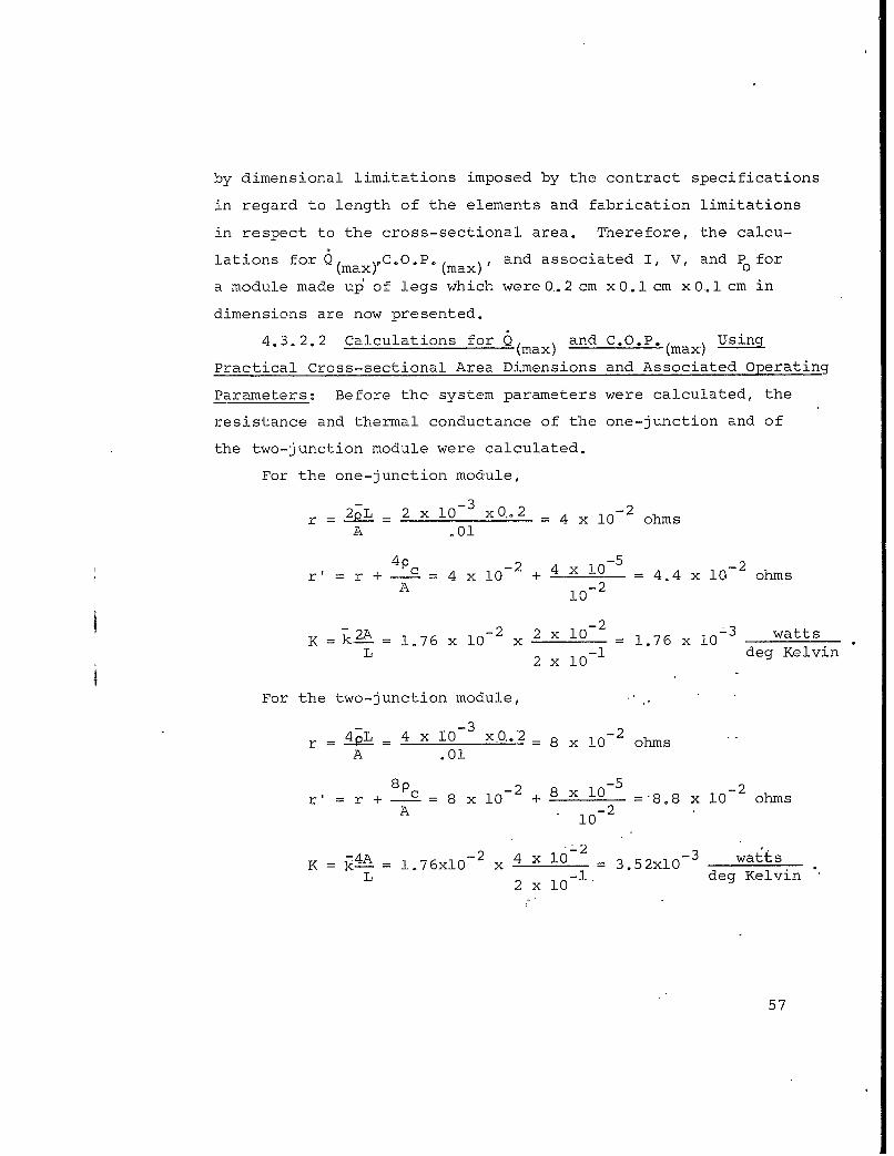
4.3.2.2 Calculations for Q(max) and C.O.Po(max) Using
Practical Cross-sectional Area Dimensions and Associated Operating
Parameters: Before the system parameters were calculated, the
resistance and thermal conductance of the one-junction and of
the two-junction module were calculated.
For the one-junction module,
r =2L 2 x 10-3 X 0..2 = 4 x 10⁻² ohmsA .01
r' =r + -= 4 x 10 2 + 4xl0 5 _ 4.4 x 10² ohmsA 10-2
K =k 2A= 1.76 x 10-2 x x10- 1.76 x 10 wattsL 2 x 10⁻¹ deg Kelvin
For the two-junction module,
r 4 L= 4 x 10⁻³ x.O.. 2 8 x 10 ohmsA .01
r' = r + , 8 x 10⁻² + 8 x 10⁻⁵ -8.8 x 10⁻² ohms
A 10-2
K = O4A 1.76xl0 -2 x 4x10 3.52xi0 3 wattsL 2 x 10- deg Kelvin
57
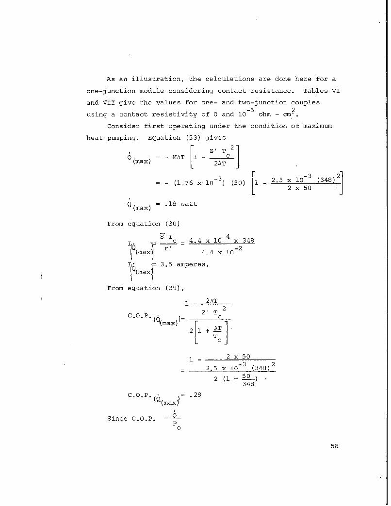
As an illustration, the calculations are done here for a
one-junction module considering contact resistance. Tables VI
and VII give the values for one- and two-junction couples
-5 2using a contact resistivity of 0 and 10 ohm - cm'.
Consider first operating under the condition of maximum
heat pumping. Equation (53) gives
(max) =-KAT - C2AT
(1.76 x -10 -) (50) _ 2.5 x x01 (348)21
Q . 18 watt(max)
From equation (30)
STc 4 . 4 x 10 4 x 348
(max 4.4 x 10²
I• x 3.5 amperes.(max
From equation (39),
1 2ATZ'T
C.O.P. ((max))= 'T c
1- 2 x 50-3 2
= 2.5 x 10 (348)
2 ( + 50)348
CO.P. =.29Q(max j
Since C.O.P. - 6P
0
58
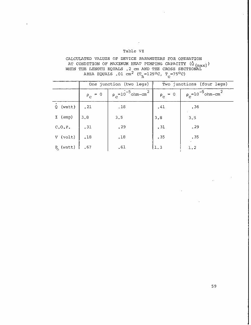
Table VI
CALCULATED VALUES OF DEVICE PARAMETERS FOR OPERATIONAT CONDITION OF MAXIMUM HEAT PUMPING CAPACITY (Q (max))
WHEN THE LENGTH EQUALS .2 cm AND THE CROSS SECTIONALAREA EQUALS .01 cm2 (T h=1250 C, T =75 0 C)
h c
One junction (two legs) Two junctions (four legs)
S=10-5 ohm-cm PC 0 p=lO 5ohm-cm2Pc = 0 c P =
Q (watt) .21 .18 .41 .36
I (amp) 3°8 3.5 3.8 3.5
CoOoPo .31 .29 .31 .29
V (volt) .18 .18 .35 .35
PC (watt) .67 o61 1i3 1.2
59
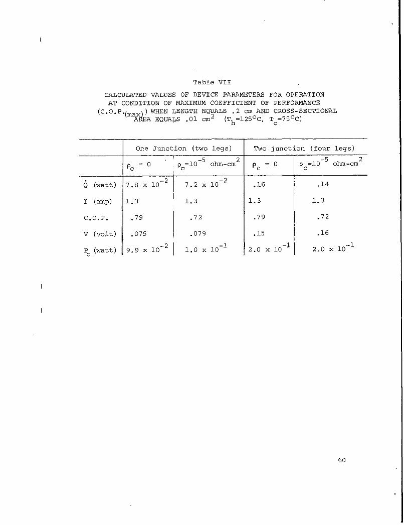
Table VII
CALCULATED VALUES OF DEVICE PARAMETERS FOR OPERATION
AT CONDITION OF MAXIMUM COEFFICIENT OF PERFORMANCE
(C.O.P.(, ) WHEN LENGTH EQUALS .2 cm AND CROSS-SECTIONALmax)"AREA EQUALS .01 cm2 (T h=1250 C, Tc=75 0 C)
One Junction (two legs) Two junction (four legs)
P = 0 =10-5 ohm-cm c = 0 P=lO-5 ohm-cm2
Q (watt) 7.8 x 10.2 7.2 x 10⁻² .16 .14
I (amp) 1.3 1.3 1.3 1.3
C.O.Po .79 .72 .79 .72
V (volt) .075 .079 .15 .16
P (watt) 9.9 x 10⁻² 1.0 x 10- 2.0 x 10- 2.0 x 10-I
60
PQp.Q _(max)
o(Q(max) CoOoP. (Q(max)
. 18
.29
P(Q a 61 watt.
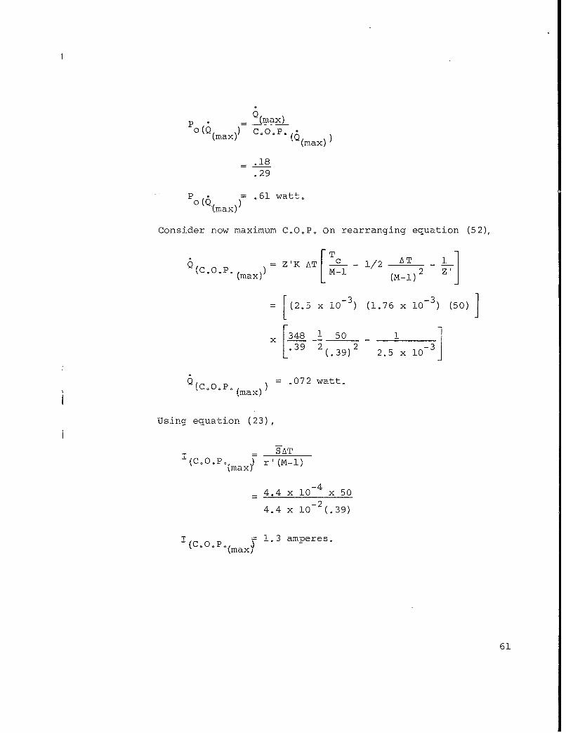
Consider now maximum C.O.Po on rearranging equation (52),
= z'K AT T /c A/2 T A
(c.o.P (max) I M-1 (M-1) 2 Z'
= [(2.5 x 10⁻³) (1.76 x 10⁻³) (50) ]
x 348 1 50 1392(.39) 2 2.5 x 1
Q(coOoP * ) .072 watt.(co..(max)
Using equation (23),
_ SAT(CO.P O(max r' (M-)
4°4 x 10-4 x 50
4.4 x 10- 2(.39)
I(C.O.Po(ax 1.3 amperes.
61

Using equation (26),
_ T [M~TlT(°''max) ATI M
[1.39 - 3981348 348
50 2.39
C.O.P. = .72(max)
Again
P QC o.o° (max)lo(C.O..Po ) C.O.P.()
(max)m
.072.72
p o(co.P.( = 10 watt.
(max)
Tables VI and VII summarize these results.
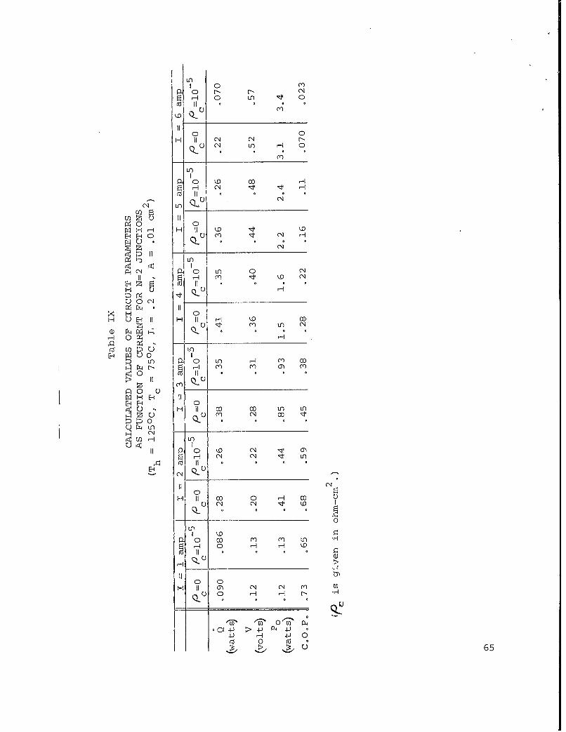
4.3.2.3 Calculation of Q, C.O.P.,0P and V as Function of
Current for Practical Dimensions: The next calculations were made
to find the variation of Q, C.O.P.,Po# and V with current I under
type IV operating conditions using the dimensions in the previous
calculations. The equations of these parameters as a function
of current are:
__ 2Q = ST 1- 1/2 1 r' - KAT (1)c
- 2ST I - 1/2 I r' - KAT
C.O.Po = c
2SATI + I r' (4)
62

P = SATI +1 2rl (3)0(2)
V = S-AT + Ir'.
These were calculated for values of current from 1 to 6
amperes. Tables VIII and IX summarize these results. Figures 3
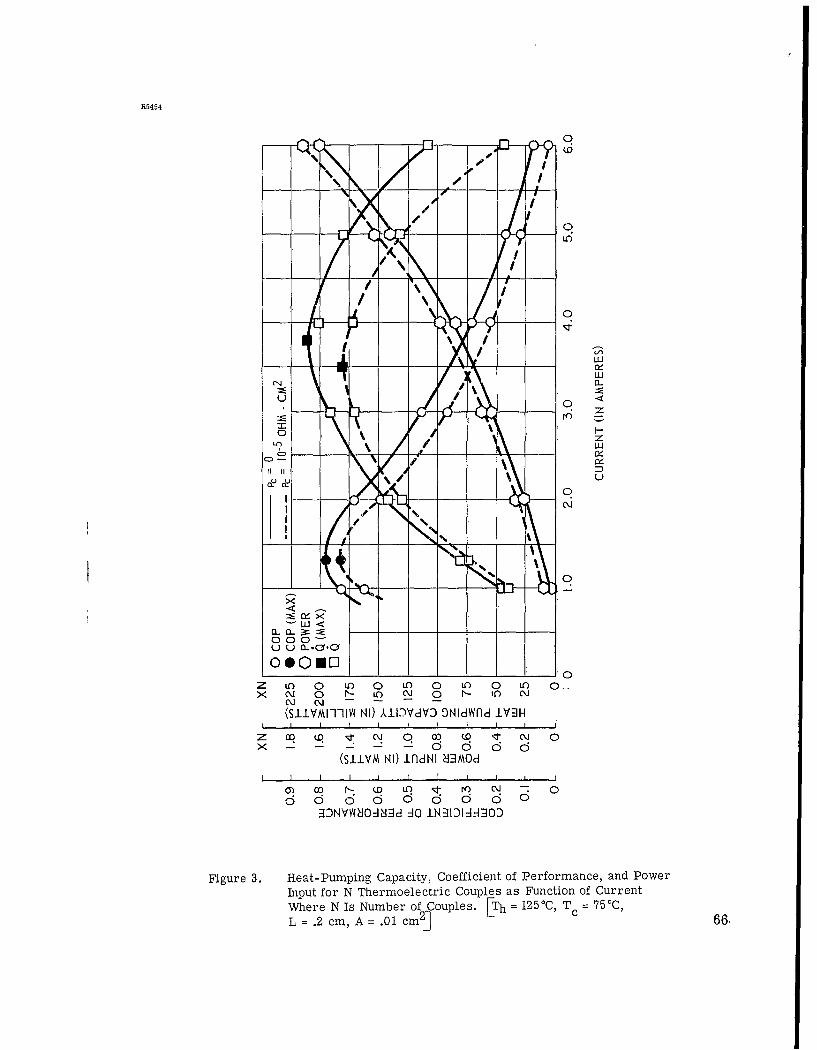
and 4 show curves of the basic parameters as a function of
current.
4.3,2.4 Estimated Performance of Couples Under Types I
to IV Operating Conditions: We now calculate the device per-
formances under types I to IV operating conditions as set forth
in SCL-7635o These conditions are summarized in table X.
Using equation (1) for type I, we have:
6 ST I - 1/2 I 2r' - KATc
5 x 10- = (4.4x10⁻⁴) (333)I-1/2.IJ4.4xl0 -2)-1.76x10⁻³ (25)
I = °35 ampere.
Using equation (2),
V = SAT + Ir'
= (4.4 x 10⁻⁴) (25) + (.35) (4.4 x 10⁻²
V = 27. mv.
Because power is equal to the product of voltage and current,
P = IV0
= (.35) (27)
= 9.4 mw
63
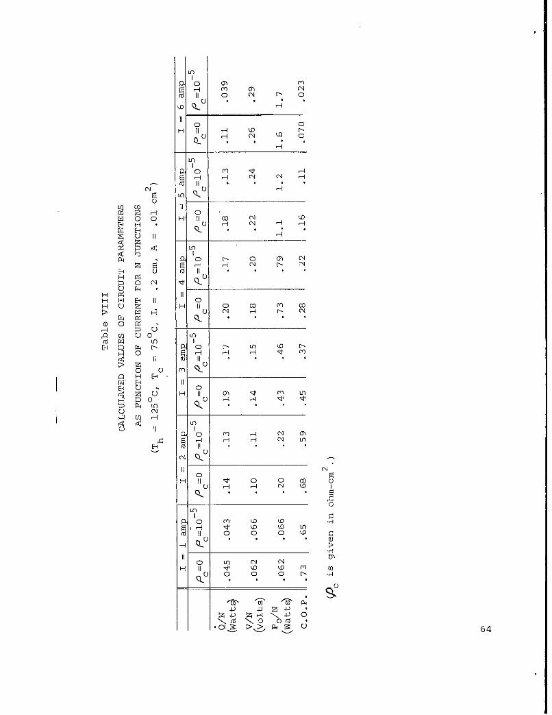
CU)
0 0
U~ -i (N 0
in
o mn
Cr4 Cl) I
0 00 OH 0I~ (
E-1 H ~ -
P4 0 N- 0 G C (
z r ri I!HýD 0Q(N
H H E-1 1H U ~0 00 Cr) 0
a) 0 PýHQ U U 0 -L
ro 14 n I
0- r:4 co N i ~S0 u H &oj
E -1 Iz. U - - m0L
w~ L. n Q *
u ciný q U ) II
II (
0- 0 50O H H (N 0 1
0in
0D m C
rd 0 0 0CD
0 in) (N (NlH I'~ D D m U
C) 0 0 0 r- -1
- -U
-l) If a
Z4-) 4H 4-) 1"(~d \" 0 0 (d
*~Ž >~ a~ U64
F4 -0 In NT 0
0i 0
U LO 4
ID
P-0 0 0H --I C') C'
U) C') 11H 0(4 0
E-1 E- 0 (ncq ) -
ID P4
uf~' 0 In
H I U P H I ~ H ID 10
H) rZ )
ý 0
0) (/ ") 0 .
E- WJ~ In1
J n 0 In r-I co cf
0 I
Qo 0
Pq H E-100 00 ID C' n
U) -i L
0
o C, C) I
00 II o- 00 u
o oo
0 0 HrHN .
P- 0 00
0 0Ž' 0-
R5454
0
LO
4 °
A I I/
00
0LU-
10
LJ
0
Z i10 0 Lr) 0 Lo 0 '1O 0 10O 0>< N~ 0 r- 10 N~ 0 r- to N~
, N/
(SiYMI-1lIW NI) AiI2WVdVD ONidcfld LVI-HX I IQ 0
(SI'IJM NI ifdN1 NJMd
I I I I I
0) Co t1- (. 0 j r) N 0
7 t. d t 0tt 0 0t 0 t .
9JNVWŽINxd JO .N. .I..dOd
Figure 3. Heat-Pumping Capacity, Coefficient of Performance, and PowerInput for N Thermoelectric Couples as Function of Current
Where N Is Number of Couples. [Tb = 125°C Tc= 75°CL = .2 cm, A = .01 cm 2] =66
R5455
0- (oSI
, Z---- /-
0 /
U)
a- Q_
z
Ol' U
U U n.-(Y.o106000
0 o 0 0 0 0 0 0 0 0 00 L) 0 LO 0 i) 0 n) 0 U-)i) t 'It n n) N) N - -
(SLLVMI71W NI) AJIDVdVD ONIdWnd iV9HS I I I II I I I I I
o 0 N aJ Qo 0* N CO co 0,- N) • Nd N N - - 0 0
(SJ_.LM NI) .LndNl •l9MOd
I I I I I I 1 I I I I
--DNVW•IO=II=d -I0 JN:IJIDI-9=OJ
Figure 4. Heat-Pumping Capacity, Coefficient of Performance, and Power InputFor Two (N=2) Thermoelectric Couples as Function of CurrentETh = 125°C, Tc = 750 C, L= .2 cm, A = .01 cm 2 ]
67

Table X
PERFORMANCE REQUIREMENTS FOR THERMOELECTRIC THERMAL-
BARRIER, MICROELEMENTS(SCL- 7635)
Type T TUnit h c
I 85 0 C 6 0 °C max 5 mw <3 amps
II 850C 60°C max 50 mw <3 amps
Iii 125°C 750C max 10 mw <3 amps
IV 125°C 750C max 50 mw <3 amps
68
PO
5 mw9,4 mw
C.0.P. = .53
Table XI summarizes these results for type I conditions,
together with those for types II, III, and IV. It should be
noted that the TEB elements for achieving type I and II con-
ditions consist of one couple, while those for achieving type
III and IV contain two couples.
Comparison of the theoretical results of table XI for type
IV TEB requirements and table IX and figure 3 clearly indicates
that a device based on the dimensions used in the calculations
would have 1a4 values in excess of those required to meet the
performance requirements (table X) on Q for currents under three
amperes. This observation also applies to the less-demanding
types 1, I! and III TEB requirements, Thus the thermoelectric
leg dimensions used in the calculations (0.2 cmx 0o1 cmx 0o1 cm)
were employed in the construction of the devices.
4.3.3 Confiqurational Design
The mechanical configurations of the TEB devices are
naturally based upon a standard micromodule substrate. The
substrate is metallized in the center to the maximum allowable
dimensions of 0,210" x 0.210", This is to help the heat transfer
through the ceramic from the thermoelectric hot junction. The
same area is allowed at the cold junction to permit adequate
space for the mounting of the heat-sensitive components, A thin
glass shell is placed around the periphery of the active area to
reduce convection, to strengthen the assembly, and to keep out
the plastic resins used in potting the micromodule stacks.
69
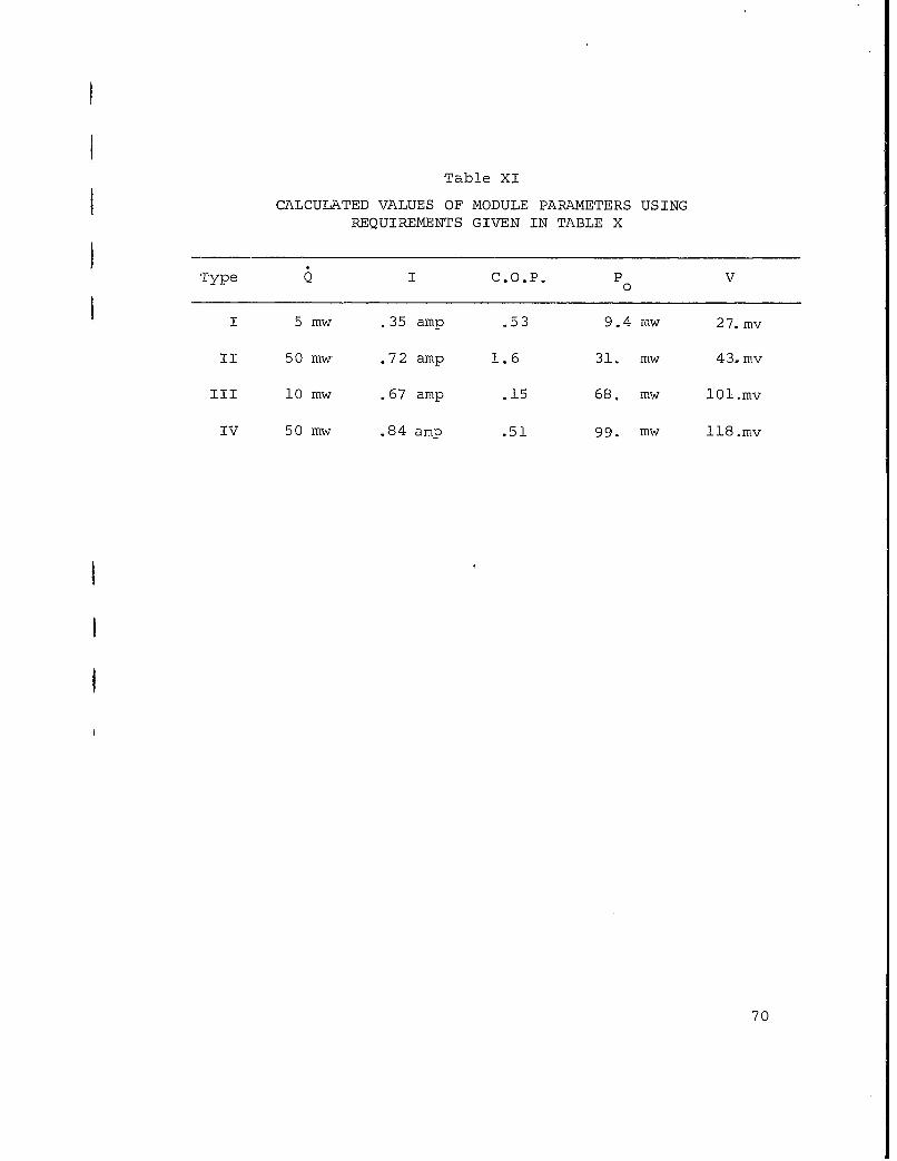
Table XI
CALCULATED VALUES OF MODULE PARAMETERS USINGREQUIREMENTS GIVEN IN TABLE X
Type Q I C.O.P. P V
I I 5 mw .35 amp .53 9.4 mw 2 7.mv
II 50 mw .72 amp 1.6 31., mw 43.mv
III 10 mw .67 amp .15 68. mw l0l.mv
IV 50 mw .84 amp .51 99. mw llS.mv
I
70
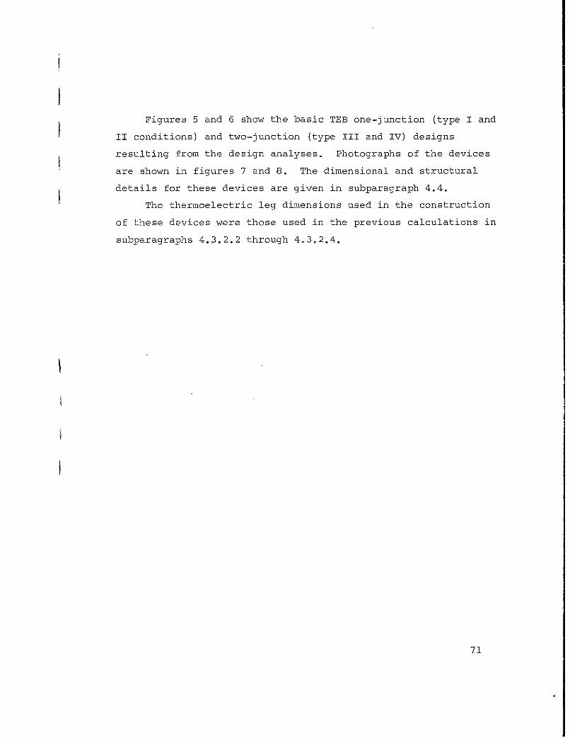
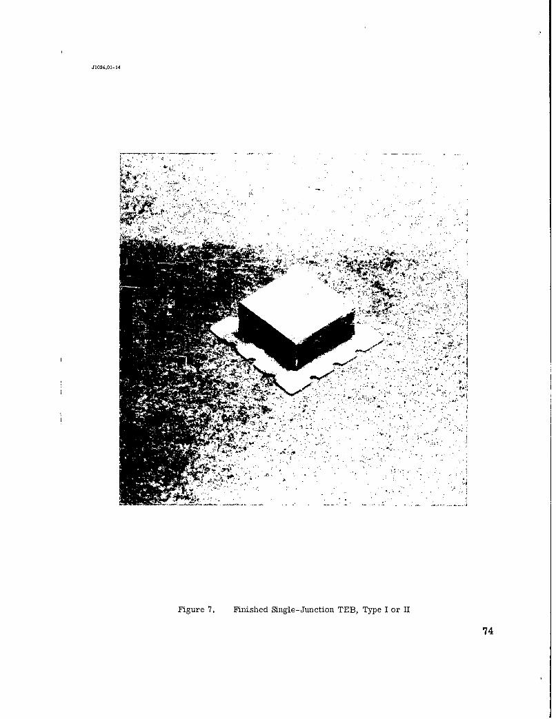
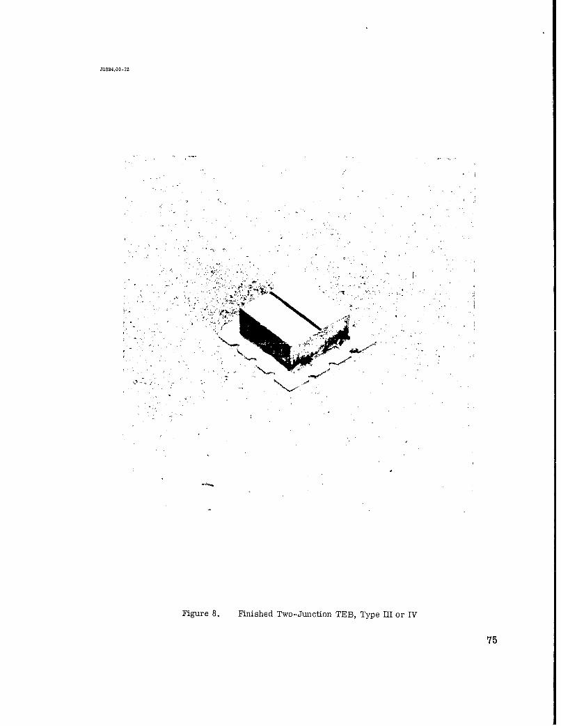
Figures 5 and 6 show the basic TEB one-junction (type I and
II conditions) and two-junction (type III and IV) designs
resulting from the design analyses. Photographs of the devices
are shown in figures 7 and 8. The dimensional and structural
details for these devices are given in subparagraph 4.4.
The thermoelectric leg dimensions used in the construction
of these devices were those used in the previous calculations in
subparagraphs 4.3.2.2 through 4°3°2.4.
71
R5456
'0.310"
0.210"NP
Figure 5. One-Junction TEB, Type I or II
72
R5457
0.31o0
0.210"
. rr- - - i r
MAX
Figure 6. Two-Junction TEB, Type III or IV
73
J1034.01-14
Figure 7. Fin-ished Single-Junction TEB, Type I or IT
74
J1034.01-12
Figure 8. Finished Two--Junction TEB, Type III or IV
75
4.4 Fabrication
4.4.1 Thermoelectric Material Source and Preparation
4.4.1.1 Sourceý The thermoelectric material used in
the performance of this contract was obtained from Materials
Electronics Products Company (Melcor), Trenton, New Jersey.
4.4.1.2 Frfpration, The thermoelectric material used
consisted of n- and p-type alloys in the quasiquaternary
system Bi xSb xTe Se (where 0 < x < 2 and 0 < y < 3) based2- x 3-y y. ..
on Bi Te This quasiquaternary system was first surveyed
under the direction of the principal investigator of the present
program at the Franklin Institute during 1957 and 1958.
It is a standard practice in the thermoelectrics industry
for materials suppliers to withhold the exact composition,
doping, and preparation steps from users as proprietary infor-
mation 7 •his has been true regarding the materials acquired
for the performance of this program. The supplier would not
release this information. Therefore,. it is not possible to
supply this information on materials used in this program.
This material will be referred to as n- or p-type Bi 2Te3 alloy.
4.4.2 Thermoelectric Material Parameters
The pertinent thermoelectric materials parameters, as
measured by the Z-meter technique on typical materials used
in the performance of this program, follow. This technique
is discussed in subparagraph 4.4.3.3.
4.4.2.1 Pit_2e Allo ,]•__n-_
a. Seebeck coefficient, S = -215 pv/ K.
b. Electrical resistivity, p = 9.75 x 10⁻⁴ ohm-cm.
co Thermal conductivity, k = 1.66 x 10⁻² w/cm-K.
d, Figure of merit, Z = 2.85 x 10- 3 ( ol.
76
4.4.2.2 Bi2Te3 A1o,__TYPe:
a. Seebeck coefficient, S = 205 Pv/°K.
b. Electrical resistivity, p = 7.50 x 10⁻⁴ ohm-cm.
C. Thermal conductivity, k = 2.01 x 10 w/cm-K.
d. Figure of merit, Z = 2.78 x 10 1K)l.
4.4.2.3 Materials Figure of Merit Z: Using the values
given above and the formula
(Sn - S p)2
Pnkn + _\pk)
Z[[(-215) - (205)] 10-6
_l.66x107 + V7.50x104x 2.01x10 2)
-3 o -l1Z = 2.83 x 10 (°K)
4.4.3 Device Process and Evaluation
A detailed description of the process for making Thermo-
electric Thermal-Barrier Microelements having performance equal
to or greater than that specified for types I, II, III, and IV
TEB's in U.S. Army Signal Corps Technical Requirement SCL-7635,
dated 29 September 1961, and summarized in table X, follows.
4.4.3.1 Summary of Process Steps; The process steps are
given in the process flow chart, figure 9. The Bi 2Te3 alloy
thermoelectric material is prepared or purchased before the
following device-processing steps.
Step 1. Evaluation of thermoelectric material ingots.
Step 2. Slicing of thermoelectric material into pellets.
Step 3. Lapping of thermoelectric pellets to desiredthickness.
77
Rl4696
zui
I-
z F-
U 0
u w
2 Zz
U, 0
Z UL
Z-JW
LLi
>- < U
CO- Z- (
.-- i ED 0~~Jz uJ
Li('Z.-
w~
Fiue9 lo hr f Eircs
z7
Step 4. Tinning of thermoelectric pellets with con-tacting alloy.
Step 5. Dicing of thermoelectric pellets into elements.
Step 6. Inspection and addition of contacting alloyto thermoelectric elements.
Step 7. Assembly into TEB's.
Step 8. Encapsulation.
Step 9. Evaluation and testing.
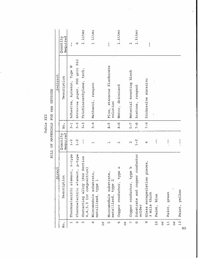
4.4.3.2 Bill of Materials for TEB Devices: The bill of
materials is summarized in table XII.
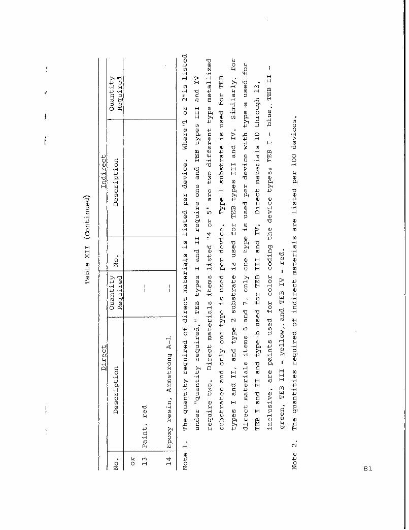
4.4.3.3 Process Description: The Thermoelectric Thermal-
Barrier Microelements, types I, II, III, and IV, are prepared
in nine basic processing steps and three subassembly processing
steps. The thermoelectric elements are formed into the desired
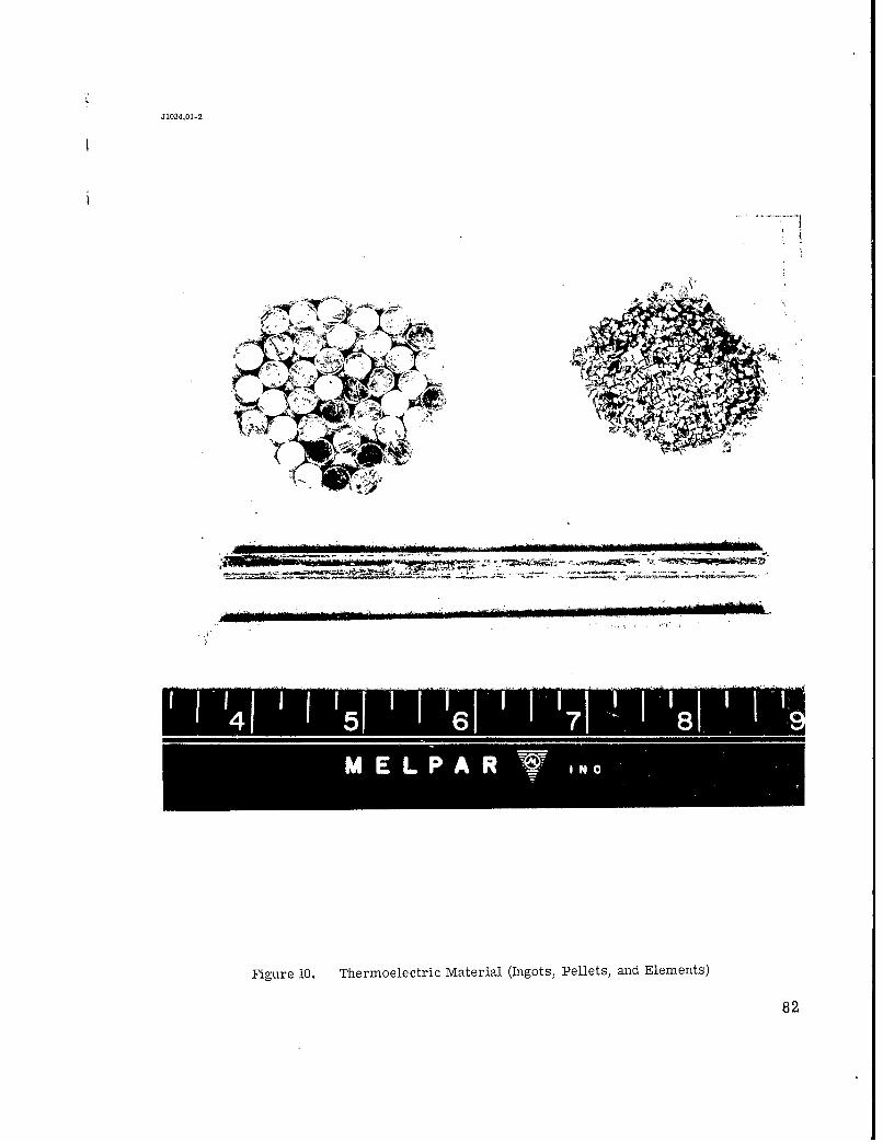
rize and shape by mechanical means (see figure 10). Low con-
tact resistance and high mechanical bond strength are obtained
through the use of a special contacting alloy and flux. The
device is assembled using a simple jig to hold the parts in
position during the bonding operation. Finally, the device
is partially encapsulated using a thin glass (microscope cover
glass) shell to seal off the inner portion of the TEB from
convection currents and restrict the entry of subsequent
encapsulants into the inner portion. The glass shell also
provides additional mechanical rigidity to the devices. See
figures 7, 8, and 11.
Step 1. Evaluation of Thermoelectric Material Ingots
1.1 Equipment
1.1.1 Thermoelectric material Z-meter(see text)
1.1.2 Seebeck coefficient meter, Model112B, Cambridge Systems, Inc.,Newton, Mass.
79
ý4 ý4 ý4
4-2 42) 4-) 4>1 10 -1 -1 r4
- 42H HH4-)-r I ~00
a P
4J >i b ( 0 0
o) S0 p 4-2 0Q H01 0 0 00-H42 -HO 0 -)H0i
'0 q- 0 0 ~ Q0 44I ' 042 U).,-I N - 0 a) (1 *H 0 rd
Wl H ý4 W ý4 H- 0i Ci N 42 Q) ý
U Cl) Q-4 PA, 0 1 0 0 0 0dH a) ( d 4-) ý4 0l 0 0 Q)
> a)0 l *H 8 4 a)i- 0 - 0 a)
w w $ýi H- 4J0 S 0 HO --ý> ý> 0 0 W 0 rd a) CC)Hq -- H H- r. H ri H .0(n Ci) 0ý I -4J ý4 ý 0 ý4
rc 4 * H 42 OH r 4J 4J 0 ) -Ho rQ ', a) 0 HO Cd 0 u H
H 01 0ý E- En II
Z C' c') m' U-) I'D r- OD 0
E-1~
EH H424JHC~ (N N I
N00q -I I- Hl HI N
0 00 Q
H1 0 0 4-)
4J 4J -HI I 42 JI
4J QC) '0 0p 5O - w 0 a)
0424 0 Q) Q) 0 0 40l 0l OH- 0) Q PA Q4 0
-*H l a) Q D 0P 04 42 42 >1 >, $-4q 0 r8 r: U) -H m (a 4-) 4-) 0)
H 0) 0D - C ) r-H .4 CNJ 042) H- H- 0 42 4J - -i
P4 a) w >1 Q, In a) in C a) ý4 0 4J.H 08 5 qP- Q ,0A. 0 0 0 fuI-4 0 Cu HO 0 :1>9 0>i4-2 420 -H -H U U) 4-3 I U4J 0 C) '0U) Ii ý4 (0 0j 0 0 r., 0 0O) 4242 V - 0a)- 0)- '0 '0 0d Q4C ) ) -H
u 00 ) OO H0 H'0 -4 07, rH 0l 0o H, -a) r. 44- (0 0 ( 0 0 0) 0, Hý -1 4 a)"H H 0 H N 'o N u 0 42) r 04J, rQ ' >1
00 42C' M O H 0 -H ( a)00 0 .u 8FH ý - 4 -I ý4 ý4 (a)
ýt8 mrno 0- 1 0 4J20 r-I 42 421 4ý4 -ý4fO ý4(d 04 P4 COrO U) -H O 0 0
W 0 : "t 0 42 04-) P4~ P4O 08 H- M r-0v rs,00 -H -HOa la 0 0 0 H: 0 0- 0d(d f
E-4 E-1 U~ It :8 C4z r ) U En 10 CO' a4 P- P
oq H o C'4l C) U-) in W 4 N W w ) 0 ý4 H 4 CN
0 0 HA OH OH 0r
80
4-) a) 0 ý4U) N 4-P 0
-Hq H L>1 rC , > P H
4-)WQ H .- 4 14 -
.r 4U) rO E-4 -q Q) (y4-)H *Hj rq ) 42 U) r-4r.C -: C) ) ý4 (d C)
rd ~ ~ tyo ar -4 C E-1C: )W LP-4 *H t0
cy 14 ý H a) F, )O H Q4 'C -Hq WDoWQ
H >, a) CJ) P4 ý --1 42 U) >94 r-4 U)
W ) 42 42 Q)
1 ) -H H 42 r-4
4 4H H Wa)
C) Q E-4 -H r- p) -H P- 00) 0 W rdC 42 H-H ý4 -1
H42 -Hq ) r o Wq H- W 42 .U
'C) P- > 0)o C) 'Cd m) W aWr) *H W3 42 U) Un r4 P4 PH- ý-i 'C ) W1 W >1
C) 5C ) W 1 Q-4 W 42 42 'CU) ý4 0 ý4 >, P4 ) W)
'C) a) W 40 ) 0)4W W 4JP) (D W- 'C) ý U)
C)4 >9 a)W -Hq -H *rd~C -Hq in E-q W u) Q >
-Hq W ) E-ý P ) W:42 42-1 V 'C) ar. U) WD 0 * ý4 U) p0 *H p w 0 -H >; W1 0o
C)I rq Q4- H -,CEa H- > 'C)P Q1C r-4
H -H 'C D 0 )W >9 r) tp 0)lH 'C W rd U) 4- ) fi r. -H
0 -*( U) C) 42 C)q *H QC)0) -: H W U) r. H 0 ý4 42
-H H- rH 04 -H O H U
r) >i'M W U) U) 'Ci W >9 4E- W 42 W 5 W 42 -1 0 >42
Ir- I4 10) 04 C) U) M) r, r- H U42 -H- I I r= >9 42 C)5 ý 0 0 W)r. C5 42 -H 4-2 (- ) mm0v 42 U) U) -0 -H::j 0) U) CQ U) -Hq QC r- L14 p E-1 o
W) pq -1 ): 0 iC)ý4 E-1 0O G) U) 'C) d 4-4 rq -
-H -H 04 (1)0) CrC) : >1 C' 0) U) rd 0 4~4
Q) 042ý C)W 04-4 ') 42) W) 0 U)
O W a ) W Q~~) C) Q) P4C9):-4 ýi r) >9 U) 0rd rq - 0 42 5 0) EO r-')
42 q ) C) 4-2 W) a14 41 r -HC) ý4 010C >1 rd 4J >1 rC) W C
) 1 -H W) 0) r-I1 : C -H 4-) *Hr >iC) C) 4 ý4 C) 0) m)
0 rq 0- 0) P4~ -- 4C0 42) 4 42 'C) H (d0 Wo H) U
-Hq ,) -H C) H -H H4 )42 r= >9 4J *d 0) 4 H fa H -HqP, 4-l 42) r, 0 'Cd w H 42
V- 2 C 4- ) 0) M 'C o ) W 42)O: 4- rC) r1 42 ~> r C
) 'Cd -H C) 42i (aCW) U) 01 44 -Hq 42 U) U H C) 0
4-i W ) C) U) W) W) Wý4- a) 'C 01, rQ P -i ý 4 P W W ) Q
,c) Z. ) W C >9 -H C0) r) 4- C4-2 >9 E-4 C) ý4 U) 42- ') rO P -H 1 E-4
-H 0
Q) Q)
O 0 - -4 0 0z Iz 81
J1034.01-2
41 F57 1 16 7171
Figure 10. Thermoelectric Material (In gots, Pellets, and Elements)
82
J10 34 .01-1
C71
0VV
F~gue 1. DiectMateial Invlve in EB
83
1.1.3 Two-point resistivity meter, Model113-2, Cambridge Systems, Inc.,
Newton, Mass.
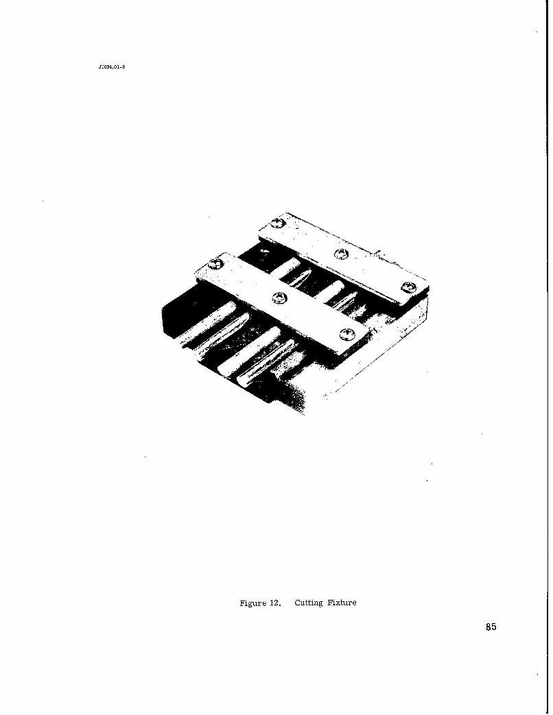
1.1.4 Crystal slicing machine, Model WMA-2,Micromech Mfg. Co., Union, N.J.
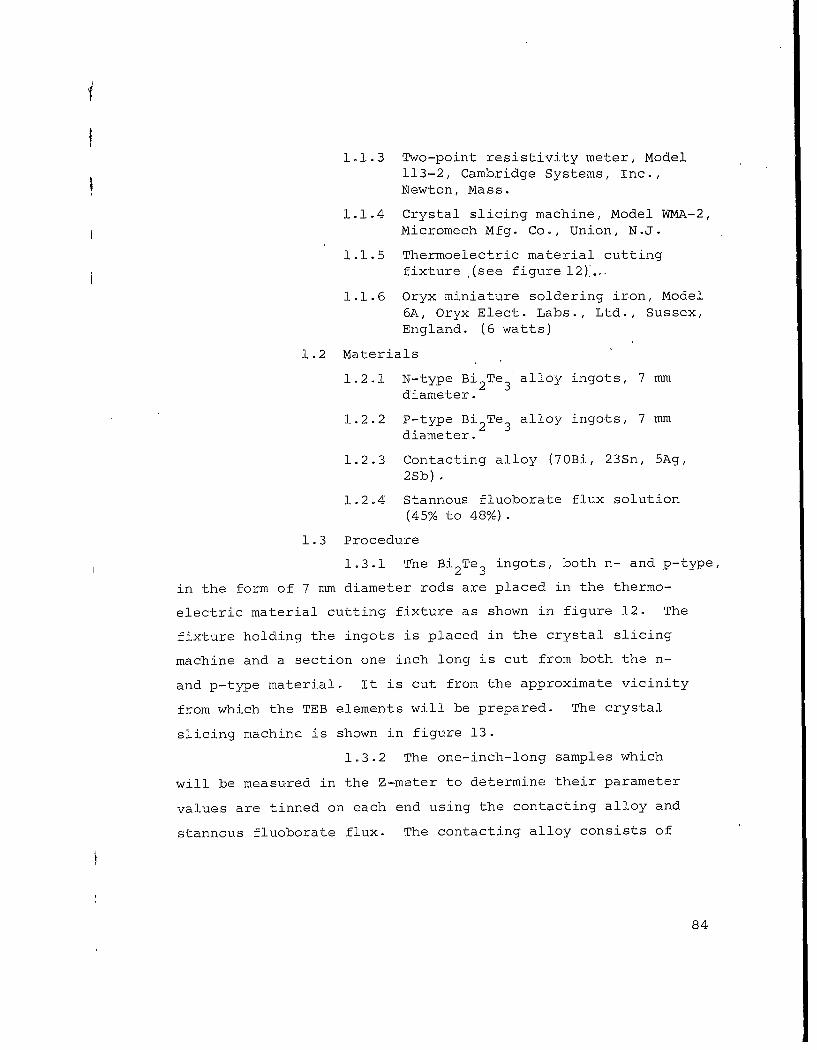
1.1.5 Thermoelectric material cuttingfixture (see figure 12).,..
1.1.6 Oryx miniature soldering iron, Model6A, Oryx Elect. Labs., Ltd., Sussex,England. (6 watts)
1.2 Materials
1.2.1 N-type Bi 2Te3 alloy ingots, 7 mmdiameter.
1.2.2 P-type Bi 2Te3 alloy ingots, 7 mmdiameter.
1.2.3 Contacting alloy (70Bi, 23Sn, 5Ag,2Sb).
1.2.4 Stannous fluoborate flux solution(45% to 48%).
1.3 Procedure
1.3.1 The Bi 2Tel ingots, both n- and p-type,
in the form of 7 mm diameter rods are placed in the thermo-
electric material cutting fixture as shown in figure 12. The
fixture holding the ingots is placed in the crystal slicing
machine and a section one inch long is cut from both the n-
and p-type material. It is cut from the approximate vicinity
from which the TEB elements will be prepared. The crystal
slicing machine is shown in figure 13.
1.3.2 The one-inch-long samples which
will be measured in the Z-meter to determine their parameter
values are tinned on each end using the contacting alloy and
stannous fluoborate flux. The contacting alloy consists of
84
J1034.01-8
Figure 12. Cutting Fixture
85
2006-3921
Figure 13. Semiconductor Crystal-Slicing Machine
86
a mixture of 70% Bi, 23% Sn, 5% Ag, and 2% Sb. They are tinned
using an "Oryx" soldering iron.
1.3.3 The samples are mounted one at a
time in the Z-meter. The Z-meter is shown in figure 14. The
evaluation is carried out, yielding values for S, p , k, and Z.
Material whose Z is less than 2.7 x 10⁻³ ( K)- is rejected
for use in the TEB application. No upper limit is set.
The Z-meter used was based upon the technique reported
by Harman [34] . The unit provide's a high vacuum with a radiation-
shielded bell jar. Thermocouple and electrical feedthroughs
are used to bring the measurement voltages out of the vacuum.
The exact technique used is explained in detail in reference [34].
1.3.4 To determine the relative uniformity
of the ingots to be used, additional measurements of Seebeck
coefficient, S, and electrical resistivity, p , are made by
probing the entire length of the ingot section to be used.
The ends of the ingots are tinned in the same manner as
described in procedure 1.3.2. A two-point probeis used to
measure p with the current contacts made to the tinned ends
of the ingot (figure 15). For the S measurement, a heated
probe which has a constant temperature differential between
the probe and the base block holding the ingots is probed along
the length of the ingots in the region to be used (figure 16).
Step 2. Slicing of thermoelectric material into pellets
2.1 Equipment
2.1.1 Crystal Slicing Machine
2.1.2 Thermoelectric material cuttingfixture
2.2 Materials
2.2.1 N-type Bi 2Te 3 alloy ingots, 7 mmdiameter.
87
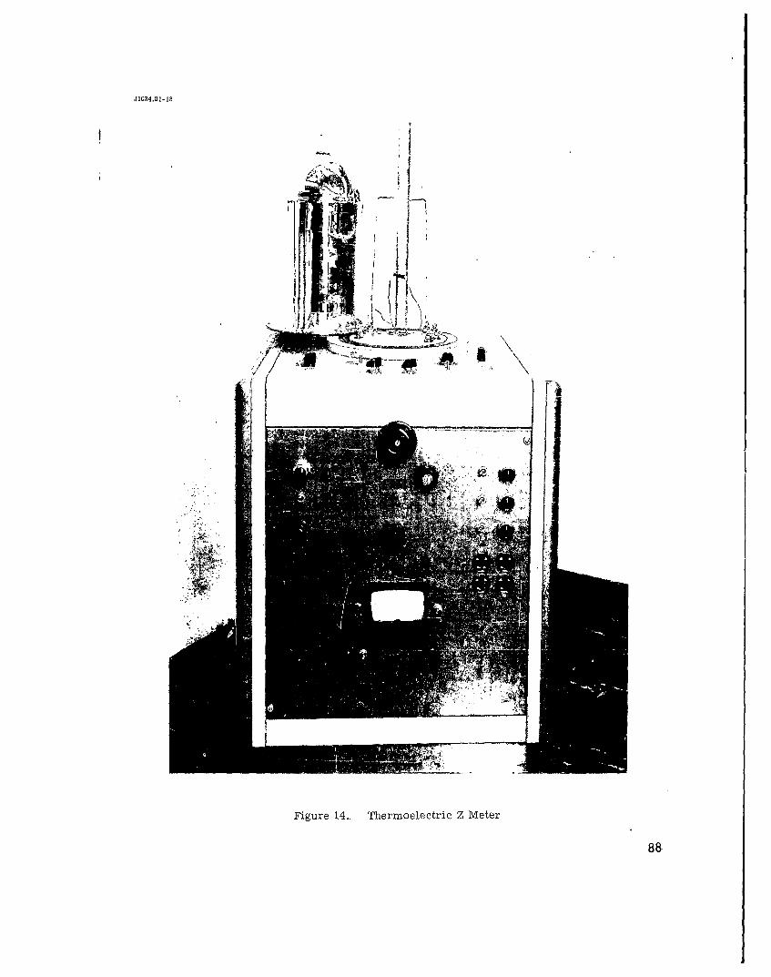
J1034.01-18
Figure 14. Thermoelectric Z Meter
88
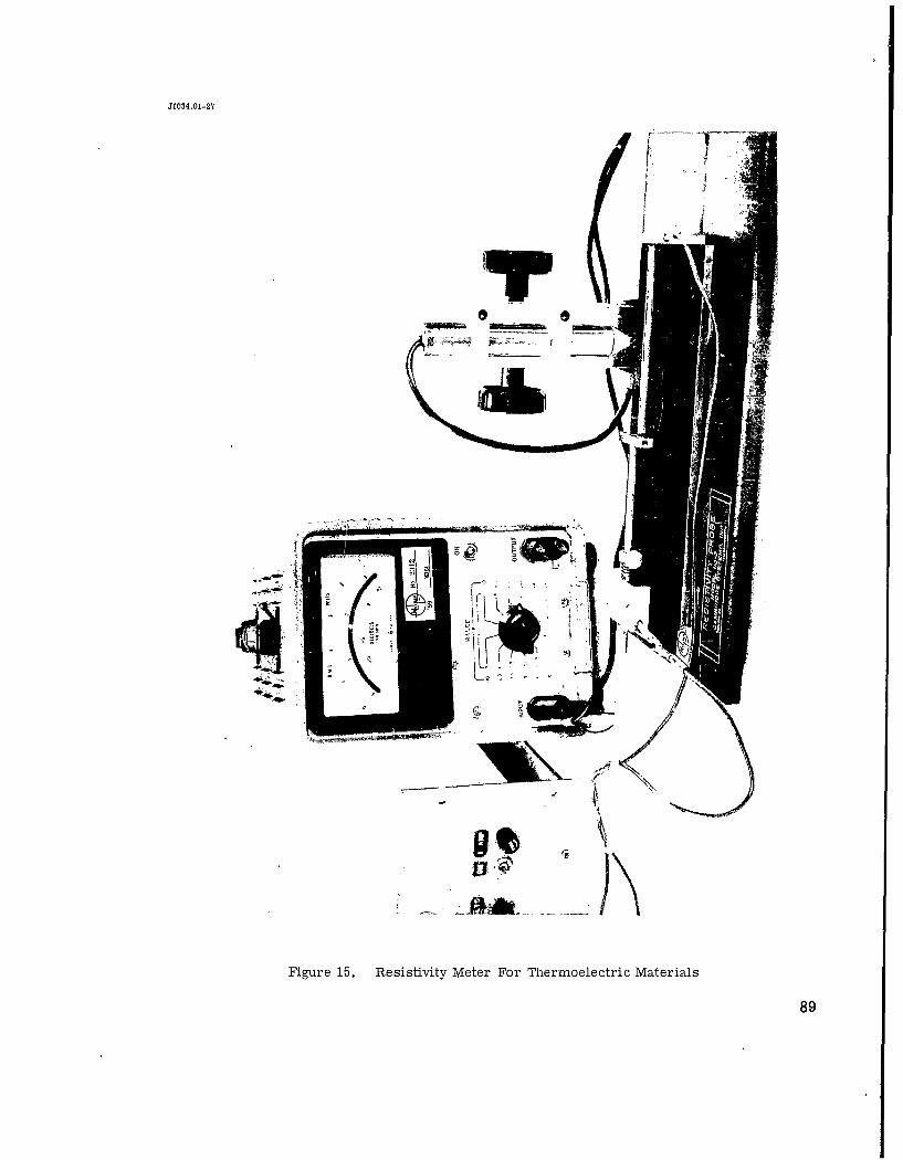
J1034.01-27
I J
iý[
Figure 15. Resistivity Meter For Thermoelectric Materials
89
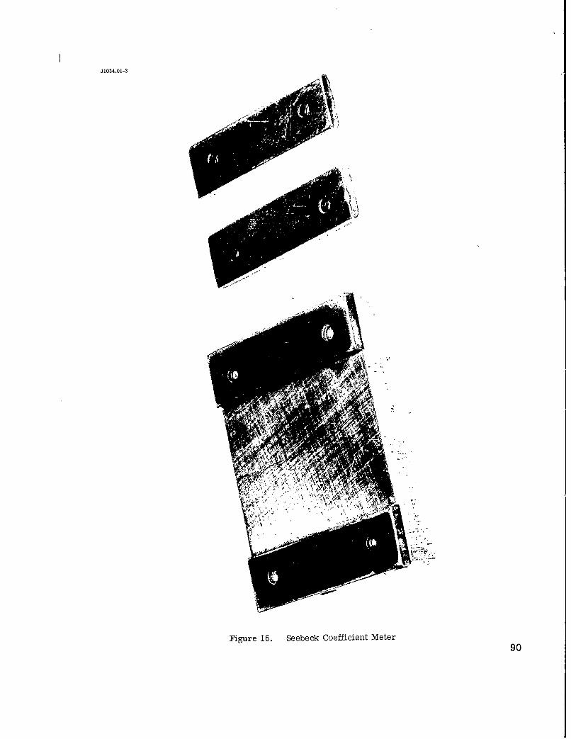
J1034.01-3
7;A
Figure 16. Seebeck Coefficient Meter90
2.2.2 P-type Bi 2 Te 3 alloy ingots, 7 mmdiameter.
2.3 Procedure
2.3.1 The n- and p-type Bi Te alloy ingots2 3
are placed in the thermoelectric materials cutting fixture
(figure 12). This fixture is placed in the crystal slicing
machine and pellets are sliced off using a 3" x 0.010" diamond+0.002"
blade to a length of 0.090" _0.00,. It is not necessary to-0.0001"keep the two types of material separate at this point so, for
convenience, they are kept together.
Step 3. Lapping of the thermoelectric pellets todesired thickness
3.1 Equipment
3.1.1 Buehler grinding wheel, 8", Buehler,Ltd., Chicago, Ill.
3.1.2 Thermoelectric material lappingfixture (see figure 17).
3.1.3 Hot plate, Temco Model 1900,
Thermolyne Corp., Dubuque, Iowa.
3.1.4 Surface temperature thermometer,
Model 573 cm, Pacific TransducerCorporation, Los Angeles, Calif.
3.1.5 Micrometer caliper, 1" (calibratedto 0.0001").
3.1.6 Tweezers, coarse point.
3.2 Materials
3.2.1 N- and p-type Bi 2 Te 3 alloy pellets,7 mm dia. x 0.090".
3.2.2 Adhesive, Apiezon type W.
3.2.3 Abrasive paper, 8" dia. discs, 600
qrit SiC.
3.2.4 Trichloroethylene, technical grade.
3.2.5 Methanol, reagent grade.
91
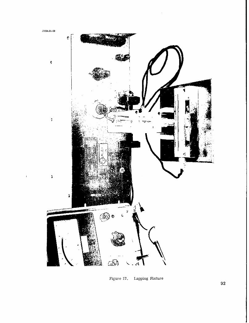
J 1034 .0 1-23
Figure 17. Lapping Fixture92
3.3 Procedure
3.3.1 The 7-mm-diameter x 0.09011 thermo-
electric pellets are mounted, using tweezers, on the thermo-
electric material lapping fixture with a very thin film of
Apiezon W. No attempt is made to differentiate between n-
and p-type material at this stage. Figure 17 shows the lapping
fixture. The Apiezon W is a thermoplastic material which melts
between 80 and 90 C. The temperature is measured with a
surface-temperature thermometer. This operation is performed
on a hot plate which is set at approximately 90 0 C.
3.3.2 The lapping fixture is composed
of two sections. One is the base upon which the elements are
mounted close to the surface with a thin film of adhesive.
The other is two sets of two hard steel gauge plates which
control the thickness or length to which the pellets are lapped.
The gauge plate set is mounted with one gauge plate at each
end of the base piece. The first set of gauge plates is thicker
than the desired pellet length. These are used to finish
one side of the pellets and to leave enough material to finish
the other side. With the first set of gauge plates installed,
the pellets are lapped on the Buehler rotary grinding wheel
on 600 grit SiC abrasive paper. Water is used as a coolant
and to carry away the Bi 2Te3 which is lapped away. The pellets
are lapped until the gauge plates come down onto the lapping
surface.
3.3.3 The lapping fixture and pellets
are rinsed with water and dried. The fixture is placed back
on the hot plate and the pellets removed. The Apiezon W is
cleaned from the elements and the fixture with hot trichlorbethylene.
93
The pellets are rinsed in methanol and dried. They are then
turned over with the recently lapped side down and mounted
to the lapping fixture base in the manner previously described
in procedure 3.3.1. The other set of gauge plates is installed.
These plates are the thickness to which the pellets must be
finished.
3.3.4 The pellets are lapped on this side
until they are lapped flush with the finish gauge plates. A
micrometer is used to check each pellet to ensure that each
is coming down evenly. The fixture and pellets are again
rinsed with water and dried. The pellets are removed and
cleaned as described in procedure 3.3.3. After cleaning,
they 'are checked again with micrometers and any pellet outside
the limits 0.079" to 0.080" is rejected or reprocessed.
Step 4. Tinning of thermoelectric pellets withcontacting alloy.
4.1 Equipment
4.1.1 Oryx miniature soldering iron, with
stainless steel tip, 0.020" diameter-
4.1.2 Hot plate.
4.1.3 Surface-temperature thermometer.
4.1.4 Tweezers, coarse.
4.2 Materials
4.2.1 N- and p-type lapped Bi Te alloy
pellets, 7-mm-diameter x 0.080".
4.2.2 Contacting alloy.
4.2.3 Stannous fluoborate flux.
4.2.4 De-ionized water.
4.2.5 Methanol, reagent grade.
94
4.3 Procedure
This is a critical step because the quality
of the electrical contact is determined by correctness of the
following operations.
4.3.1 With the hot plate set at 190 0 C,
as measured by the surface-temperature thermometer, a thermo-
electric pellet is placed on the hot plate and stannous fluo-
borate flux is applied to the entire top surface. The pellet
is allowed to come to temperature. As the fluxed pellet is
coming to temperature, a small quantity of contactingý alloy
(enough to form a small bead at the end of the 0.020" diameter
stainless steel soldering tip) is taken onto the small soldering
iron. When the flux is beginning to boil off of the pellet,
the pellet is held in position on the hot plate with tweezers
and the soldering iron carrying the contacting alloy is brought
in contact with the pellet surface. Immediately, the soldering
iron is moved in a manner that spreads the contacting alloy
over the entire pellet top surface. This is accomplished by
moving the iron rapidly in a small circular motion until this
motion has covered the whole pellet top surface. If some
areas do not wet completely, more flux may be added and the
process repeated. The result should be a thin even coating
of solder over the whole top surface of the pellet.
4.3.2 The thermoelectric pellet is turned
over and procedure 4.3.1 repeated on the other end surface.
The pellets are tinned at this stage to ensure good wetting
over the entire end-surfaces of resulting elements and because
greater yields of diced elements can be obtained due to the
extra strength provided by the solder.
95
4.3.3 The tinned pellets are cleaned in
hot (80 to 90 C) de-ionized water for 15 minutes. After this
treatment, they are rinsed in methanol and dried.
Step 5. Dicing of thermoelectric pellets into elements.
5.1 Equipment
5.1.1 Crystal slicing machine.
5.1.2 Dicing fixture (see figure 18).
5.1.3 Hot plate.
5.1.4 Surface temperature thermometer.
5.1.5 Stereoscopic microscope with cali-brated measuring reticle.
5.1.6 Tweezers, coarse.
5.1.7 Tweezers, fine.
5.2 Materials
5.2.1 N- and p-type tinned pellets, 7
mm-diameter x 0.080".
5.2.2 Apiezon adhesive, type W.
5.2.3 Material mounting block, Chalk Tile,Jerrill Engrg Co., Fanwood, N.J.
5.2.4 Trichloroethylene, tech. grade.
5.2.5 Methanol, reagent grade.
5.3 Procedure
5.3.1 The tinned pellets are mounted to
the material mounting block with Apiezon adhesive, type W.
This is accomplished,as previously described, on a hot plate.
The pellets are lined up in straight rows with coarse-pointed
tweezers so that a maximum number of elements may be diced
from them at one time. All the spaces between the pellets
are filled in with the Apiezon adhesive up to the top surface
and also filled up around the edges of the pellet rows. This
96
J1034.01-15
Figure 18. Dicing Fixture
97
serves to give necessary support for the cut sections and keep
them from breaking loose from the mounting block. The mounting
block is mounted into the dicing fixture. The dicing fixture
is shown in figure 18.
5.3.2 The dicing fixture is mounted into
the crystal slicing machine and 0.040" cuts are made in one
direction along the rows of pellets. The first two cuts are
checked with a calibrated microscope to ensure the desired
dimensions in resulting elements. They must be within 0.040"
+0.0005".
5.3.3 After the first cut, the pellets
are removed from the crystal slicing machine and the material
mounting block is placed on the hot plate. The thermoplastic
adhesive is melted and the cut rows are moved together such
that the space between sliced pieces is eliminated and the
pieces lie against each other. Additional adhesive is added
around the outside of the resulting congregation of thermo-
electric pieces. All sections of the thermoelectric material
that are odd-shaped or broken and that will not result in good
elements are remo-7ed at this time. The block is removed from
the hot plate and placed in the dicing fixture. The fixture,
holding the thermoelectric pellets, is placed in the crystal
slicing machine and cuts are made perpendicular to the previous
cuts. These cuts are also made to result in 0.040" wide pieces.
The first two cuts are checked with the microscope as done in
the previous dicing step. The same tolerances are maintained.
5.3.4 The mounting block is heated on a
hot plate. The resulting elements are removed with fine-pointed
98
tweezers. The elements are cleaned in hot trichloroethylene
for 15 minutes, rinsed in reagent methanol and dried.
Step 6. Inspection and addition of contacting alloyto thermoelectric elements,
6.1 Equipment
6.1.1 Thermoelectric Probe (see text).
6.1.2 Stereoscopic microscope, 30X, Bauschand Lomb, Rochester, N.Y.
6.1.3 Hot plate.
6.1.4 Surface-temperature thermometer.
6.1.5 Tweezers, fine.*
6.1.6 Seebeck coefficient meter.,
6.1.7 Resistivity Meter, Modified (seefigure 19),
Required only when thermoelectric material propexties are
changing rapidly along the length of an ingot.
6.2 Materials
6.2.1 Diced thermoelectric elements,0.040' x 0.040" x 0.080".
6.2.2 Contacting alloy.
6.2.3 Stannous fluoborate flux,
6.2.4 Deionized water,
6.2.5 Methanol, reagent grade.
6.3 Procedure
6.3.1 The thermoelectric elements must
now be separated into n- and p-types. This is accomplished
with a "thermoelectric probe." This consists of a heated
probe and an unheated probe which are electrically connected
to a galvanometer. When an element-is contacted by these probes,
a temperature difference is created and thermoelectric voltage
99
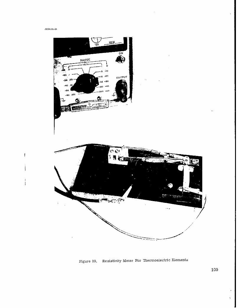
J1034.01-24
Figure 19. Resistivity Meter For Thermoelectric Elements
100
is generated. The direction of the deflection is an indication
of the polarity of the thermoelectric power (Seebeck coefficient)
of the element.
6.3.2 After the elements have been separated
into the two types, additional contacting alloy must be added
to the ends of the elements in order to obtain the desired
bonds in the finished devices. It is extremely difficult to
apply this alloy in the correct amounts during the original
tinning of the elements.
This addition of contacting alloy is accomplished by placing
a small volume of the alloy (approximately 1/4" cube) on a
microscope slide which is heated on a hot plate to 190 0 C. The
temperature is monitored by a surface-temperature thermometer.
On another microscope slide, placed beside the hot plate, a
small amount of stannous fluoborate flux is spread out in a
thin film. This is so that the elements may be coated with
a small amount of the flux at each end.
Using a stereoscopic microscope to observe the operation
and fine-pointed tweezers to handle the elements, the addition
of the contacting alloy is performed. The elements are grasped
in the middle with the tweezers and fluxed on both ends. While
observing through the microscope the element is brought into
contact with the melted hemisphere of contacting alloy and
held for one second. At the end of this time it is pulled
away rapidly from the surface of the contacting alloy. This
operation is repeated on the other end of the element. The
result should be a smooth spherical surface covering the entire
area of each end of the element, with the spherical radius
being approximately 0.030" to 0.035". As each element is looked
101
at under the microscope it is visually inspected and rejected
if found to be broken or misshaped.
6.3.3 The elements are placed in hot
de-ionized'water (80 to 90 C) as they are processed. After
the batch has been completed, the elements (now being kept
separated into n- and p-type categories) are rinsed in reagent
methanol and dried.
6.3.4 After the application of additional
contacting alloy the Seebeck coefficient and resistivity of
the elements may be checked. This operation is to be included
when gross material variations are being experienced. Because
this occurs infrequently, it is not considered necessary as a
standard part of the process. In large-scale production it
may have advantage when material from several ingot sources
are grouped together in a batch of elements.
In this operation the S-meter is used in the same manner
as it was used in the ingot evaluations. The same measurement
method is used for the resistivity as was used for the ingot
evaluation except that a smaller set of probes is used on
the elements. The probe consists of a pair of tweezers with
electrically insulated points. The current is passed through
the tinned ends of the elements and the voltage drop taken
across a 1 mm spacing at the tweezer tips. See figure 19.
Step 7. Assembly into TEB's.
7.1 Equipment
7.1.1 Assembly'jig (see figure 20).
7.1.2 Hot Plate.
7.1.3 Surface-temperature thermometer.
7.1.4 Stereoscopic microscope, 1OX.
7.1.5 Jig cooling block (brass 4" x 4" x i").
102
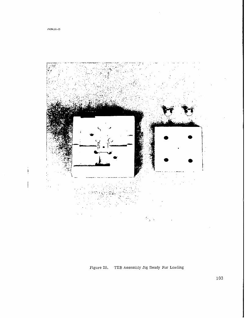
J1034.01-13
010
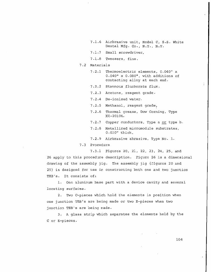
7.1.6 Airbrasive unit, Model C, S.S. White
Dental Mfg. Co., N.Y., N.Y.
7.1.7 Small screwdriver.
7.1.8 Tweezers, fine.
7.2 Materials
7.2.1 Thermoelectric elements, 0.040" x0.040" x 0.080", with additions ofcontacting alloy at each end.
7.2.2 Stannous fluoborate flux.
7.2.3 Acetone, reagent grade,
7.2.4 De-ionized water.
7.2.5 Methanol, reagent grade,
7.2.6 Thermal grease, Dow Corning, TypeXC-20106,
7.2.7 Copper conductors, Type a or type b.
7.2.8 Metallized micromodule substrates,
0.010" thick,
7.2.9 Airbrasive abrasive, Type No. 1.
7.3 Procedure
7.3.1 Figures 20, 21, 22, 23, 24, 25, and
26 apply to this procedure description. Figure 26 is a dimensional
drawing of the assembly jig. The assembly jig (figures 20 and
25) is designed for use in constructing both one and two junction
TEB's. It consists of:
1. One aluminum base part with a device cavity and several
locating surfaces.
2. Two C-pieces which hold the elements in position when
one junction TEB's are being made or two E-pieces when two
junction TEB's are being made.
3. A glass strip which separates the elements held by the
C or E-pieces.
104
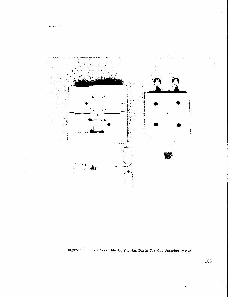
J1034.01-7
Figure 21. TEB Assembly Jig Showing Parts For One-Junction Device
105

J1034.01-4
4*Z.
Figure 22. TEB Assembly Jig Showing Parts For One-Junction Device LoadedInto Position in Jig
106
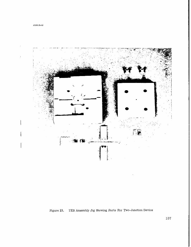
J1034.01-10
iAt
Figure 23. TEB Assembly Jig Showing Parts For Two-Junction Device
107
JI034.01-6
.Ii
Figure 24. TEB Assembly Jig Showing Parts For Two-Junction DeviceLoaded Into Position in Jig
108
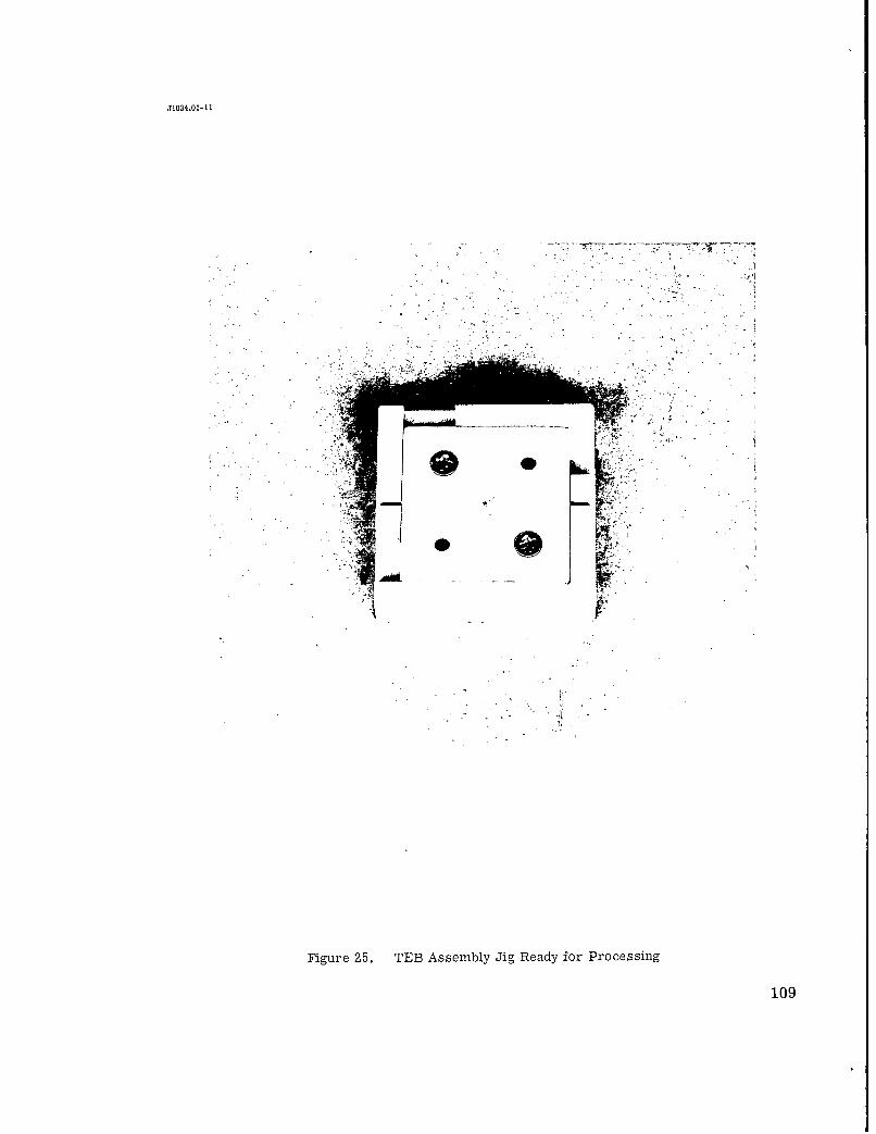
J1034.01-11
Figure 25. TEB Assembly Jig Ready for Processing
109
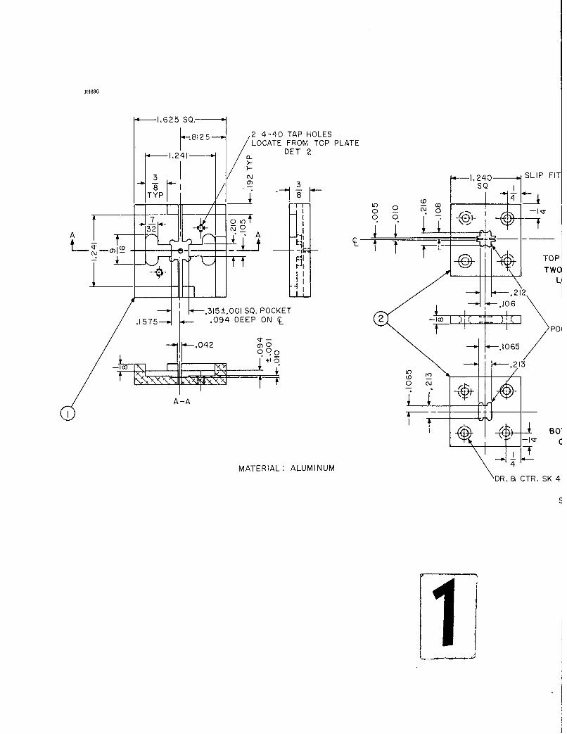
F14690
1.625 SQ.-
2 4-40 TAP HOLESK 812 5 LOCATE FROM TOP PLATE1.241 DET 2
I-1.240 SLIP FIT
O�)
(0 4
___ o 2 -
00 -�-. -YTOP�
II TW____ I L
-II
.315±.OOI SQ. POCKET
.1575 .094 DEEP ON C�
-¶4-.042oco
U +10
-�il�
A-A
MATERIAL: ALUMINUM
S
___-J
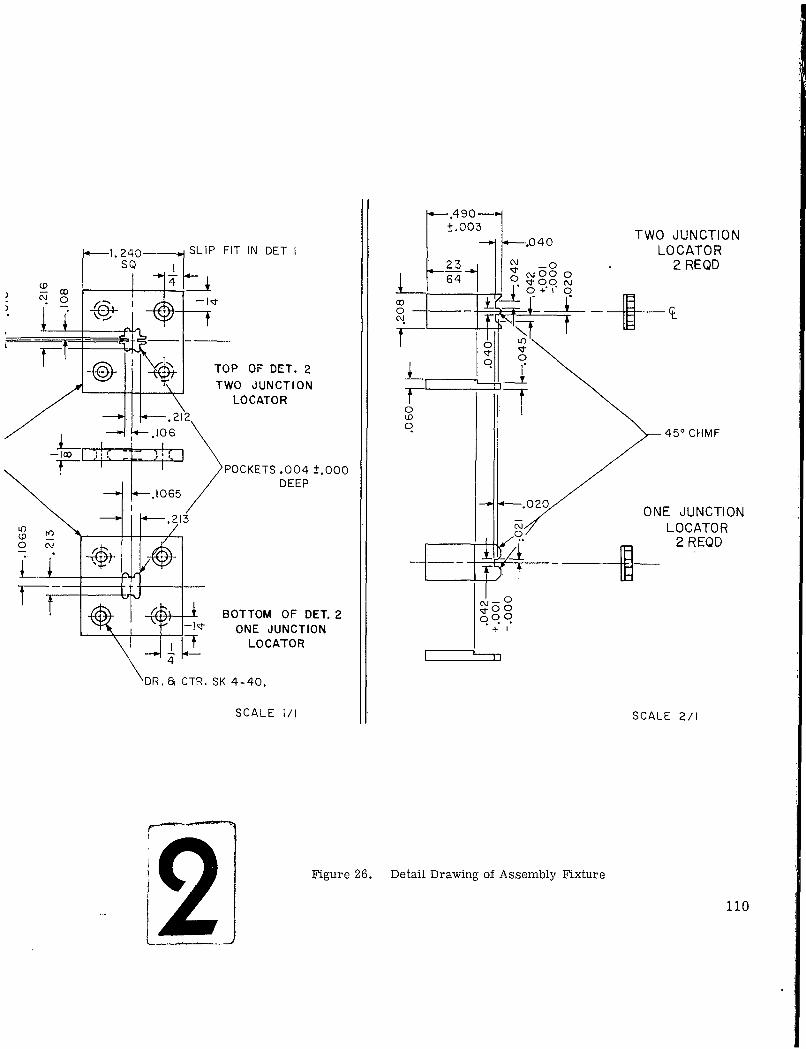
.490--±.003 TWO JUNCTION
1.240 SLIP FIT IN DET I .040 LOCATOR2 0 2 -REQD
jQ 6 4 j - 0
__ --: (g) c\j
TOP OF DET. 2
TWO JUNCTIONLOCATOR --
.2-12 (0.106 450CHMF
POCKETS .004 ±.000I DEEP-,' • -- 1065
.020 ONE JUNCTION.213 LOCATOR
0 .r 2 REQD
BOTTOM OF DET. 2 o 0-N- ONE JUNCTION +1
LOCATOR
\DR. & CTR, SK 4-40.
SCALE I/I SCALE 2/I
Figure 26. Detail Drawing of Assembly Fixture
( 110
4. A top plate which holds one type-a copper conductor
part or two type-b conductor parts. Type-a is used for one-
junction TEB's and type-b for two-junction TEB's. One side
of the top plate is cut for type-a parts, the other side for
type-b. The copper conductors are illustrated in figure 27.
5. Two 4/40 screws, used to tighten the top plate down
onto the jig proper. These are necessary to obtain the desired
overall TEB thickness.
See figures 21 and 23. The procedural difference between
making one- and two-junction TEB's is simply the use of either
C-pieces or E-pieces, loading of the proper number of elements,
the proper copper conductors and the correct side of the top
plate.
Because the assembly is similar except for the above-noted
differences, a description of the assembly of only the two-
junction TEB is given.
While observing through a stereoscopic microscope, the
parts are loaded into the jig with fine-pointed tweezers. See
figures 23 and 24. The parts are loaded in the following order
as shown in the photographs:
1. The metallized micromodule substrate.
2. The glass separator strips.
3. The two E-pieces, relieved side down.
4. Two n-type and two p-type thermoelectric elements,
highly fluxed with stannous fluoborate flux, are positioned
so that they will be series-connected by virtue of their positions
on the substrate and the two copper conductors.
The two type-b copper conductors are now placed in position
with tinned side out on the appropriate cavities of the top plate.
1ll
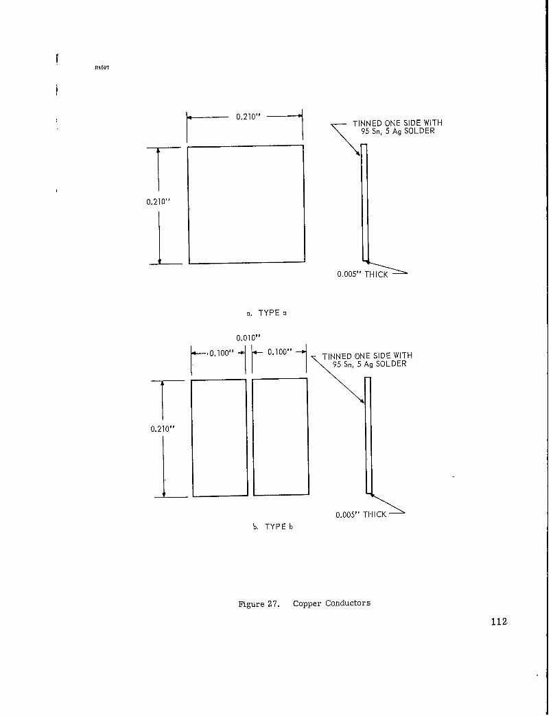
R4697
01TINNED ONE SIDE WITH95 Sn, 5 Ag SOLDER
0.210"
0.005" THICK
a. TYPE a
0.010"o
0.100" - 0.100" j TINNED ONE SIDE WITH
I 95 Sn, 5 Ag SOLDER
0.210"
0.005" THICK
b. TYPE b
Fgure 27. Copper Conductors
112
They are kept in position and held in the cavity by a thin
film of silicon grease. This concludes the loading of the
parts into the jig.
7.3.2 The base part of the jig and
the top plate are now placed on the hot plate which is held
at a temperature of 190 0 C and monitored by a surface temperature
thermometer. A small amount of stannous fluoborate flux is
applied to the copper conductors' tinned surfaces. When the
flux begins to evaporate, the top plate is placed in position
on the jig base. The plate is oriented such that the copper
conductors bear the proper relation to the elements for series
connections. By this time the contact alloy on the ends of
the elements has melted and the top may be pushed down (very
carefully and gently) until it bottoms flat against the inner
surface of the jig. The two 4/40 screws are placed in and
tightened down gently assuring absolute bottoming and flatness
of the top plate. This assures parallel device surfaces and
eliminates any excess thickness not caused by improperly sized
parts.
The surface-temperature thermometer is placed on top of
the closed jig and the jig is allowed to remain on the hot
plate until the top of the jig as measured by the surface
thermometer is at 190 C. This requires approximately one
minute. The jig is then removed and placed on a cooling block
where the temperature of the jig is reduced to approximately0
50 C in one minute.
7.3.3 The jig is unloaded. Because
of the presence of flux in the jig, the devices usually stick
in the jig. Acetone is used to free these devices by applying
a small quantity to the areas which are sticking.
113
7.3.4 The assembled TEB is then cleaned
in hot (80 to 90 C) de-ionized water for 15 minutes, then rinsed
with methanol and dried. An additional cleaning step is used.
The device is lightly blasted all over with an Airbrasive Unit,
using No. 1 abrasive. The Airbrasive Unit is shown in figure
28. This cleans the last vestige of foreign material from the
ceramic, copper, and element areas of the TEB. A final rinse
in methanol is used.
Step 8. Encapsulation
8.1 Equipment
8.1.1 Stereoscopic microscope, 20X.
8.1.2 Tweezers, fine,
8.1.3 Epoxy resin applicator (roundtoothpick).
8.l.4 Oven, 100 0 C0
8.2 Materials
8.2.1 TEB assemblies.
8.2.2 Three-mil glass encapsulation sub-assemblies.
8.2.3 Epoxy resin, Armstrong Type A-1and Activator A, Armstrong ProductsCo., Warsaw, Ind.
8.3 Procedure
8.3.1 Two glass encapsulation subassemblies,
each consisting of two 3-mil-thick pieces of glass bonded to
each other at right angles with epoxy resin (see figures 11
and 29), are used. The operation is performed under the micro-
scope. The area on the substrate which will be directly under
the glass encapsulant is coated with a narrow line of Armstrong
A-1 epoxy resin (mixed 3 drops of catalyst per gram) all the way
114
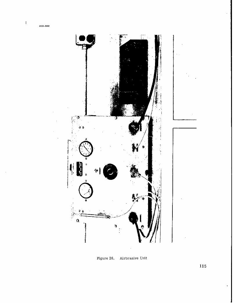
2 006-3939
I i t ,
115
Figure 28. Airbrasive Unit
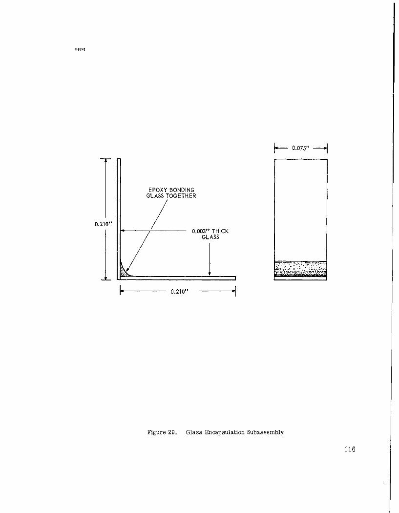
R4698
•-~~, -H
EPOXY BONDINGGLASS TOGETHER
0.210" 0
GLASS
IIL0.210"
Figure 29. Glass Encapsulation Subassembly
116

around, using a round toothpick as the applicator. The glass
subassemblies are placed in correct position on the device.
8.3.2 The units are placed in an oven
for one hour at 100°C. The TEB's are then removed from the
oven.
8.3.3 After cooling, more A-1 epoxy
is added, filling in any holes or gaps at the bottom and sealing
the glass to the copper conductors at the top.
8.3.4 The TEB's are placed back in
the oven and cured for one hour at 130 0 C. At the end of this
time, they are removed and allowed to cool.
Step 9. Evaluation and testing.
9.1 Equipment9.1.1 Vacuum System (10-4 10-5
9.. Vcu Ssem(0 -- 1 mm
Hg).
9.1.2 A-C and D-C power supplies.
9.1.3 A-C and D-C current and voltage
meters.
9.1.4 Potentiometer and sensitive
galvanometer, Model K-3, Leeds
and Northrup Co., Philadelphia,Pa.
9.1.5 No. 40 gauge Chromel-Alumel
thermocouples.
9.2 Materials
9.2.1 TEB's, Types I, II, III, and IV.
9.2.2 Thermal grease, Dow Corning
type XC-20106.
9.3 Procedure
9.3.1 Figures 30, 31, and 32 are
applicable to this procedure. To determine the performance
of TEB's the devices are tested in a vacuum system (pressures
117
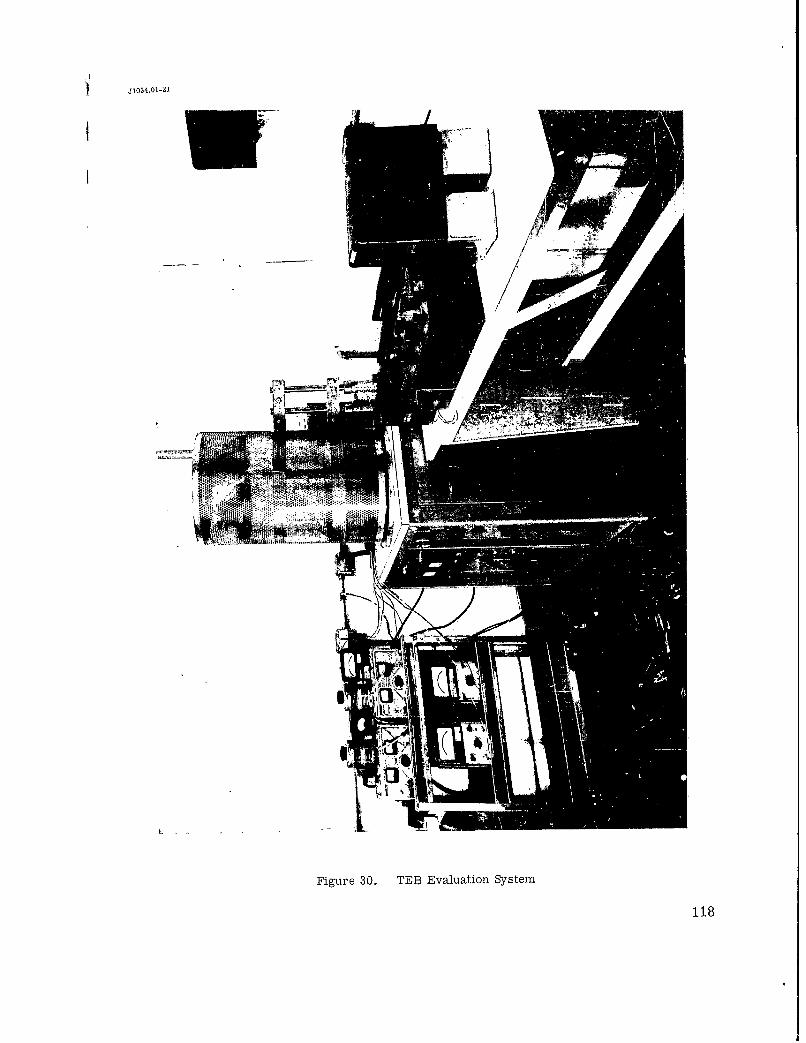
! J1034.01-21
w
Figure 30. TE.B Evaluation System
118
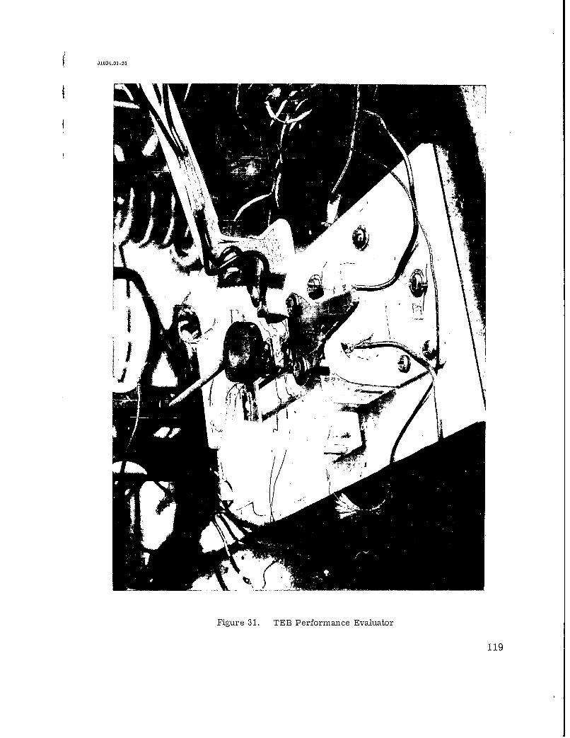
S J1034.01-25
Figure 31. TEB Performance Evaluator
119
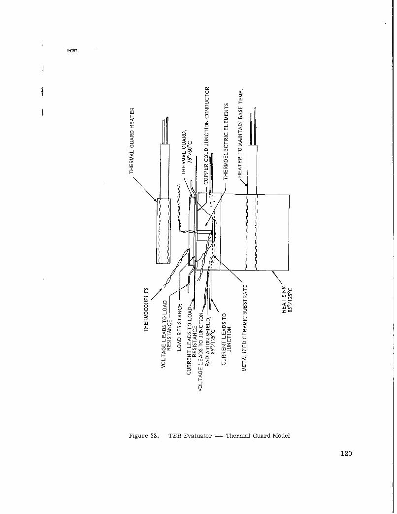
4707
U LU
uJ z 0Hi 0 wU <
LU z o0 -j
Li <0 H H
C U .0
rLU 0
LU U:-H L LU LU
U
I rol,.I rV
I I IIL U
<I z0
I I I
< 0
LU -iLU
-J Z 4
) F-(L U'40
<j LU UH- <C
0j H) 0J -- -
LU HL 0
L< <U H ZUC- LU L
7) < HOJ 0 ~ 0 , FLUJLU 0) _jý LU 0 Z ~ LU_j V) < L LU, N
HiLU 0O i:U D -
0 ck -<
LU0
-j
0
Figure 32. TEB Evaluator - Thermal Guard Model
120
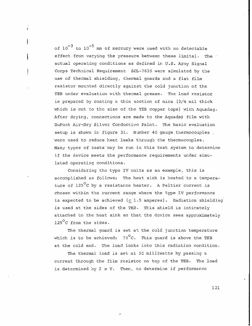
of 10- to I0 5 nun of mercury were used with no detectable
effect from varying the pressure between these limits). The
actual operating conditions as defined in U.S. Army Signal
Corps Technical Requirement SCL-7635 were simulated by the
use of thermal shielding, thermal guards and a flat film
resistor mounted directly against the cold junction of the
TEB under evaluation with thermal grease. The load resistor
is prepared by coating a thin section of mica (3/4 mil thick
which is cut to the size of the TEB copper tops) with Aquadag.
After drying, connections are made to the Aquadag film with
DuPont Air-Dry Silver Conductive Paint. The basic evaluation
setup is shown in figure 31. Number 40 gauge thermocouples
were used to reduce heat leaks through the thermocouples.
Many types of tests may be run in this test system to determine
if the device meets the performance requirements under simu-
lated operating conditions.
Considering the type IV units as an example, this is
accomplished as follows: The heat sink is heated to a tempera-
ture of 125 0 C by a resistance heater. A Peltier current is
chosen within the current range where the type IV performance
is expected to be achieved (c 1.5 amperes). Radiation shielding
is used at the sides of the TEB. This shield is intimately
attached to the heat sink so that the device sees approximately
125 0 C from the sides.
The thermal guard is set at the cold junction temperature
which is to be achieved: 75 0 C. This guard is above the TEB
at the cold end. The load looks into this radiation condition.
The thermal load is set at 50 milliwatts by passing a
current through the film resistor on top of the TEB. The load
is determined by I x V. Then, to determine if performance
121
meets the specifications, it is necessary only to measure the
temperature of the thermal load resistor. At a current of
1.5 amperes the temperature of the thermal load is usually
less than 75 C. The C.O.P. may be determined by measuring
the device voltage.
C.O.P. = -0
IV
Additional testing may be carried out if desired, such
as the measurement of the temperature of the thermal load at
various electrical currents for given values of Q. An alterna-
tive method is to adjust the current until the desired tempera-
ture of the thermal load is obtained (in this case 75 C) and
then note the current value. A reasonably accurate value for
AT(max) at 0 = 0, (neglecting radiation loss) may be obtained
by removing the thermal load and varying the current until a
minimum T is achieved. To do this, Th should be maintained
at the specified hot junction temperature. Approximate device
Z may be determined from the AT(max) measurement since:
2AT (max) = 1/2 Z Tc 2
In addition, an extremely simple and reasonably accurate
estimate of performance may be made by measuring only the
voltage drop with no thermal load and Th at the specified
temperature. The voltage drop corresponding to normal per-
formance is determined by measuring actual operating performance
as described above on several devices. A device voltage drop
deviation either higher or lower than the normal range indi-
cates a defective device. A lower voltage drop indicates bad
or degraded thermoelectric material. A higher than normal
voltage drop indicates high contact resistance. It is, of
122

course, possible to have a defective device whose voltage drop
would fall in the "normal" range. In all of the devices tested
none were found which fell in this category. The performance
of these devices can be definitely established, however, by
this simple technique if followed by the additional simple
measurement of A-C resistance. By doing this, this method
can be considered an acceptable estimate of device performance.
This type of measurement is considerably simpler and less time-
consuming than the standard technique described above, though
less accurate.
A "heat leak" type of TEB evaluation system was tried.
This method was found to be as difficult and as time-consuming
as the thermal guard system described previously. Reasonably
good agreement was obtained (10%) when the same device was
tested in both systems to determine the current that gave the
desired performance. Better TEB performance was measured using
the heat-leak system.
The heat-leak method used a hot junction heat source
similar to that used in the thermal guard system. The thermal
guards at the sides of the TEB were used as in the other system.
The resistor thermal load and cold junction thermal guard were
not used. A square cross-section piece of stainless steel
alloy 304 was used as the heat leak. The area of the heat
leak was the same as the area of the cold junction. Using
the known thermal conductivity of the stainless steel, the
distance necessary to provide a 10 0 C temperature difference
with a 50 milliwatt heat flow through the leak was calculated.
A No. 40 thermocouple was placed into the heat leak at the
required distance from the end. A source of heat was placed
at the upper end of the square stainless steel rod. This steel
123
thermal leak was placed in intimate contact against the TEB
under test, with thermal grease. A No. 40 Chromel-Alumel thermo-
couple was placed at the interface of the heat leak and the
TEB cold junction. This heat-leak system is pictured in
figure 33.
The hot junction temperature had been maintained at 125°C.
The TEB current was then adjusted to the value that gave a 10 0 C
AT between the heat-leak thermocouples. This current then
became the value at which the desired TEB performance was
obtained.
9.3.2 After evaluation, the thermal
grease and oxides are removed from the copper conductors by
light blasting with the Airbrasive Unit. The TEB's are now
ready for application.
4.4.3.4 Subassembly Operations: The following subassembly
operations are a part of the process for constructing TEB's:
a. Preparation of Metallized Micromodule Substrates
Standard 0.010" thick micromodule substrates were
purchased with a moly-manganese metallized area. See figure
34. The moly-manganese metallization is supplied plated with
copper to facilitate soldering.
The Airbrasive unit is used to cut the desired conductor
pattern in the metallization. Figures 35 and 36 show the
pattern for the one-junction and two-junction TEB's,respectively.
After the pattern has been cut, the pattern is tinned with
a thin coating of 95% Sn, 5% Ag solder using standard rosin-
alcohol flux. The flux residue is removed with methanol.
b. Preparation of Copper Conductors
Pure annealed copper, 0.005" thick, is used. It is
tinned with a thin coat of 95% Sn, 5% Ag solder using
124
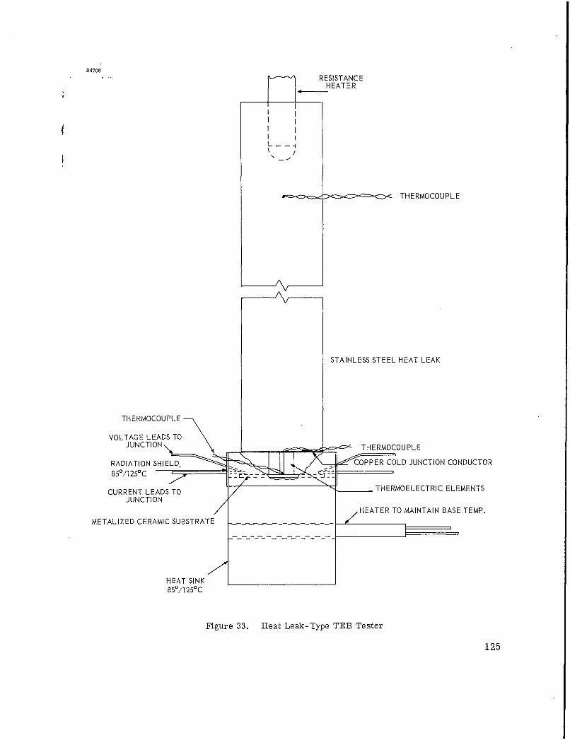
R4706
RESISTANCEHEATER
I I
THERMOCOUPLE
STAINLESS STEEL HEAT LEAK
THERMOCOUPLE
VOLTAGE LEADS TOJUNCIONNTHERMOCOUPLE
RADIATION SHIELD, - COPPER COLD JUNCTION CONDUCTOR850/I1250C
CURNTLAS TO THERMOELECTRIC ELEMENTS
JUNCTIONHEATER TO MAINTAIN BASE TEMP.
METALIZED CERAMIC SUBSTRATE
850/1 250C
Figure 33. Heat Leak-Type TEE Tester
125

R14699
~- 0.210" +00CENTER PORTION -05
M ETA LLIZED ..... ... ......... ...
0.210" 0.310"+. 000" +.004"-. 005" -. 00011
0.310" +.004"-. 000"1
Figure 34. Micromadule Substrate, Metalized
126
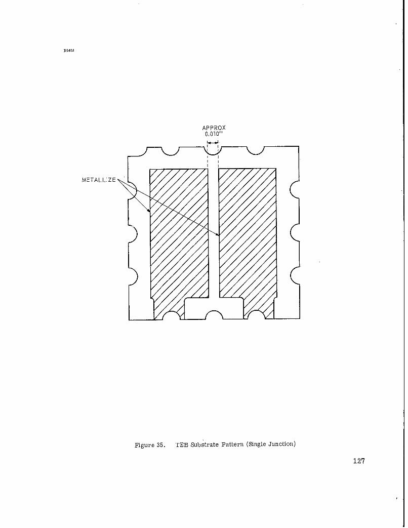
R5458
APPROX0.0101,
METALLIZE
Figure 35. TEB Substrate Pattern (Single Junction)
127

METAL LIZ E
tAPPROX
0.0101,
Figure 36. TEB Substrate Pattern (Two Junction)
128
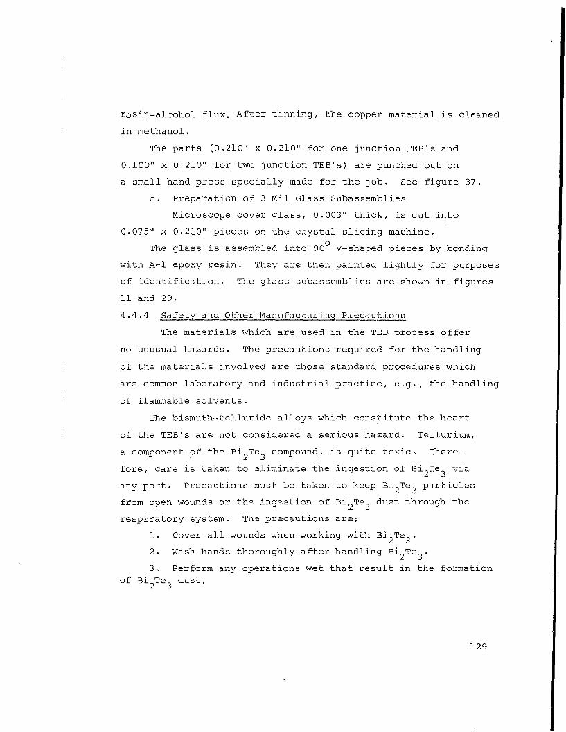
rosin-alcohol flux. After tinning, the copper material is cleaned
in methanol.
The parts (0.210" x 0.210" for one junction TEB's and
0.100" x 0.210" for two junction TEB's) are punched out on
a small hand press specially made for the job. See figure 37.
c. Preparation of 3 Mil Glass Subassemblies
Microscope cover glass, 0.003" thick, is cut into
0.075" x 0.210" pieces on the crystal slicing machine.
The glass is assembled into 90 V-shaped pieces by bonding
with A-1 epoxy resin. They are then painted lightly for purposes
of identification. The glass subassemblies are shown in figures
11 and 29.
4.4.4 Safety and Other Manufacturing Precautions
The materials which are used in the TEB process offer
no unusual hazards. The precautions required for the handling
of the materials involved are those standard procedures which
are common laboratory and industrial practice, e.g., the handling
of flammable solvents.
The bismuth..-telluride alloys which constitute the heart
of the TEB's are not considered a serious hazard. Tellurium,
a component of the Bi Te compound, is quite toxic. There-2 3
fore, care is taken to eliminate the ingestion of Bi 2Te3 via
any port. Precautions must be taken to keep Bi 2 Te 3 particles
from open wounds or the ingestion of Bi 2Te3 dust through the
respiratory system. The precautions are:
1. Cover all wounds when working with Bi 2Te3.
2. Wash hands thoroughly after handling Bi 2Te3'
3. Perform any operations wet that result in the formationof Bi 2Te3 dust.
129
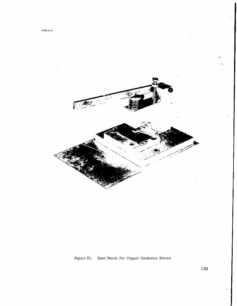
J1034.01-9
Figure 37. Hand Punch For Copper Conductor Pieces
130
One other possible hazard exists which results from heating
the material or a device containing the material to the vicinity
of its melting point (585 C). At this temperature the partial
decomposition of the compound and the sublimation of the tel-
lurium occurs. In this regard, the degree of seriousness of
the hazard is similar to that of selenium rectifier burnouts.
No normal operation results in the attainment of such tempera-
tures nor do any of the processing steps require any temperatures
great enough to cause the release of tellurium vapors.
131
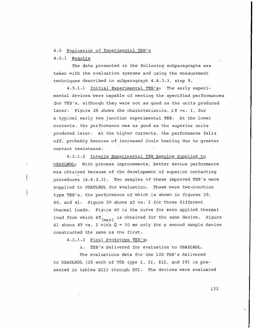
4.5 Evaluation of Experimental TEB's
4.5.1 Results
The data presented in the following subparagraphs was
taken with the evaluation systems and using the measurement
techniques described in subparagraph 4.4.3.3, step 9.
4.5.1.1 Initial Experimental TEB's: The early experi-
mental devices were capable of meeting the specified performances
for TEB's, although they were not as good as the units produced
later. Figure 38 shows the characteristics, AT vs. I, for
a typical early two junction experimental TEB. At the lower
currents, the performance was as good as the superior units
produced later. At the higher currents, the performance falls
off, probably because of increased Joule heating due to greater
contact resistance.
4.5.1.2 Interim Experimental TEB Samples Supplied to
USAELRDL: With process improvements, better device performance
was obtained because of the development of superior contacting
procedures (4.4.3.3). Two samples of these improved TEB's were
supplied to USAELRDL for evaluation. These were two-junction
type TEB's, the performance of which is shown in figures 39,
40, and 41. Figure 39 shows AT vs. I for three different
thermal loads. Figure 40 is the curve for zero applied thermal
load from which AT max) is obtained for the same device. Figure
41 shows AT vs. I with = 50 mw only for a second sample device
constructed the same as the first.
4.5.1.3 Final Prototype TEB's:
a. TEB's delivered for evaluation to USAELRDL.
The evaluations data for the 100 TEB's delivered
to USAELRDL (25 each of TEB type I, II, III, and IV) is pre-
sented in tables XIII through XVI. The devices were evaluated
132
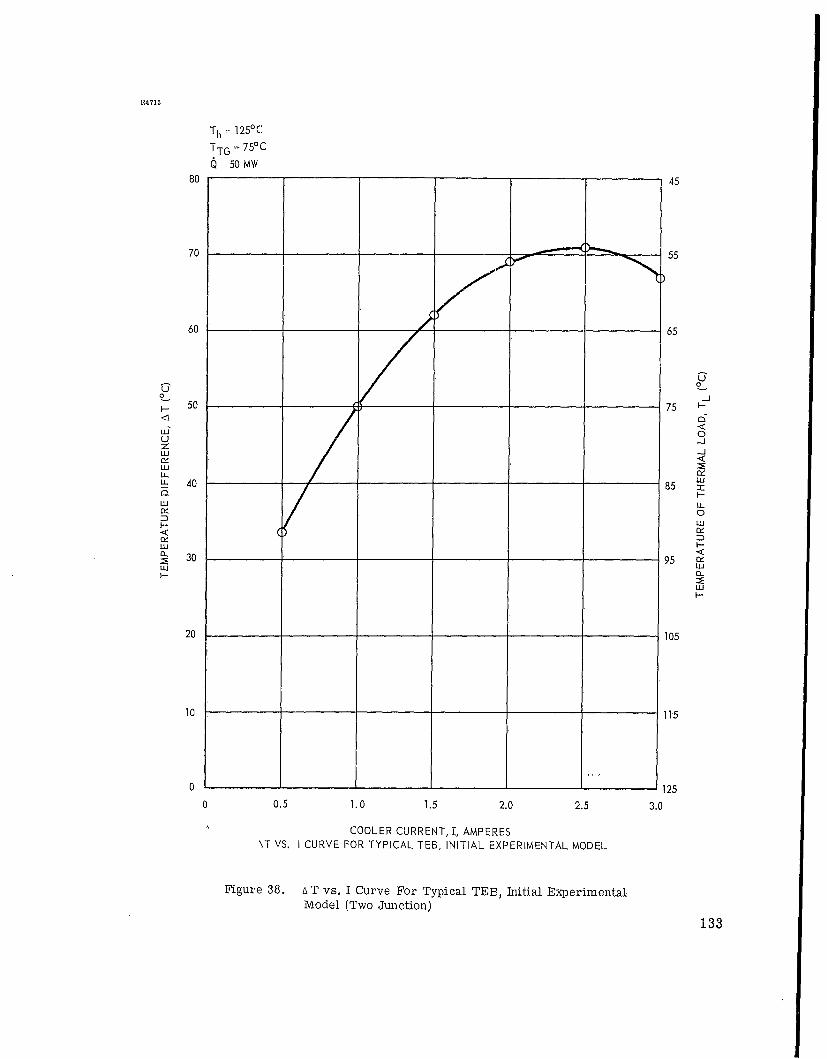
R4715
Th t- 1250C;
TTG ý 750 C
Q-50 MW80 45
70 -- _____-55
uJ
60 65
00
•_ 50 75 k
z i~
LULU
LL LJL. 40 85
QHLU LL
011 LU
LU HIL 30 95 Ov
LULUj
20 105
10 115
0 1250 0.5 1.0 1.5 2.0 2,5 3.0
COOLER CURRENT, I, AMPERES\T VS. I CURVE FOR TYPICAL TEB, INITIAL EXPERIMENTAL MODEL
Figure 38. AT vs. I Curve For Typical TEB, Initial Experimental
Model (Two Junction)
133
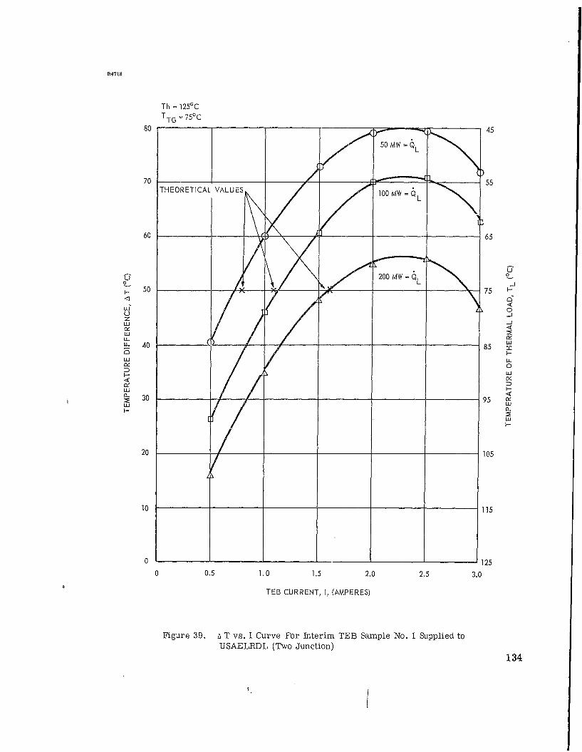
R4718
Th = 125 0CTTG = 750 C
80 4
50 MW L
07U _
w_ 0 65 -
UL
zI-L oU
L L .I I'-'
.. 30I.• LU
LLU
20 105
10 115
0 12500.5 1.0 1.5 2.0 2.5 3.0
TEB CURRENT, 1, (AMPERES)
Figure 39. A T vs. I Curve For Interim TEB Sample No. 1 Sulpplied toUSAELRDL (Two Junction)
134
w/H!
R4717
Th = 125°C
APPLIED THERMAL LOAD Q =0
100 25
AT MAX POINT
90 35
80 45
0 0 S70 55 .
I--H14-1 LU
zw I--:LU<
x4
E 60 65 ELU H-
H 0
LUULu z
: 50 75
0U
40 85
30 95
20 1050 0.5 1.0 1.5 2.0 2.5 3.0
TEB CURRENT, I (AMPERES)
Figure 40. Curve For AT(yax) Determination For Interim TEB Sample
No. 1 Supplied to USAELRDL (Two Junction) 135
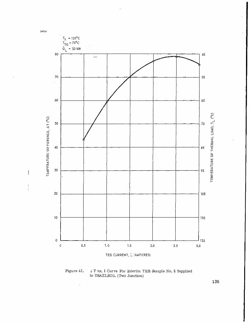
R4710
Th = 1250 CTTG =750 C
Q =50 MWSL80 l45
70 55
60 -,65
50 75 I-<6wo.0UzUI
_ 40 85
LU L0
Lii_ 30 95 fl<
95 W
20 105
10 115
0 - 125
0 0.5 1.0 1.5 2.0 2.5 3.0
TEB CURRENT, I, (AMPE~RES)
Figure 41. L T vs. I Curve For Interim TEB Sample No. 2 Supplied
to USAELRDL (Two Junction)
136
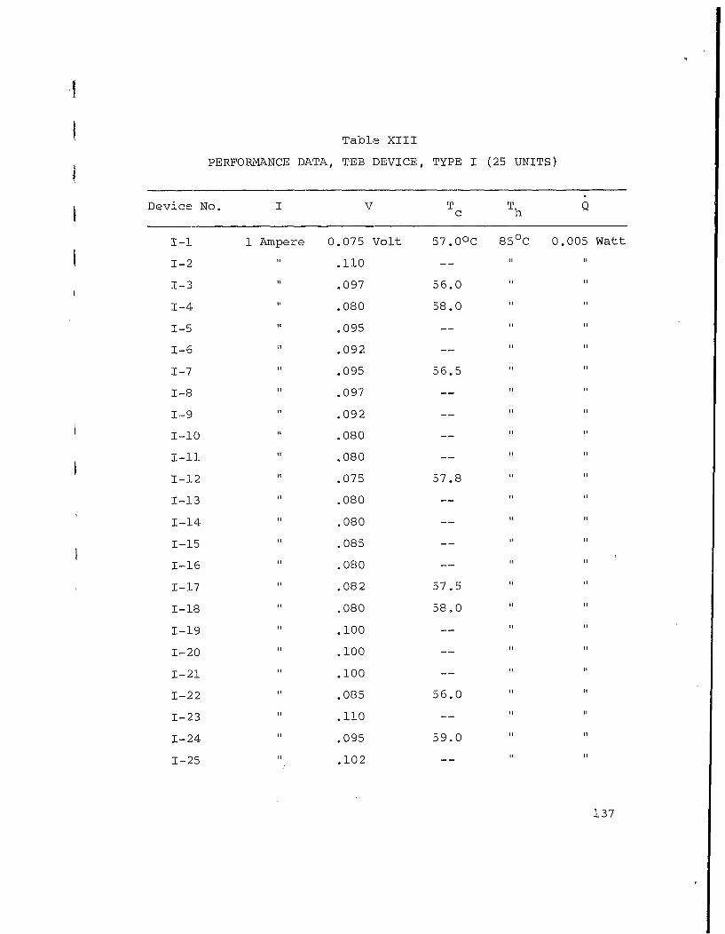
I
Table XIII
PERFORMANCE DATA, TEB DEVICE, TYPE I (25 UNITS)
Device No. I V T Th Qc
I-i 1 Ampere 0.075 Volt 57.0°C 850 C 0.005 Watt
1-2 .110 -- "
1-3 .097 56.0
1-4 .080 58.0
1-5 .095 --
1-6 .092 -- " "
1-7 .095 56.5 " "
1-8 .097 -- " "
1-9 .092 -- i "
1-10 .080 --
i-ll .080 -- " "
1-12 .075 57.8
1-13 .080 -- " "
1-14 .080 --
1-15 .085 --
1-16 .080 -- iI
1-17 " .082 57.5
1-18 .080 58.0
1-19 .100 -- I1
1-20 .100 -- ii
1-21 .100 --
1-22 .085 56.0 it
1-23 .110 -- ii ii
1-24 .095 59.0 "
1-25 .102 -- it
137
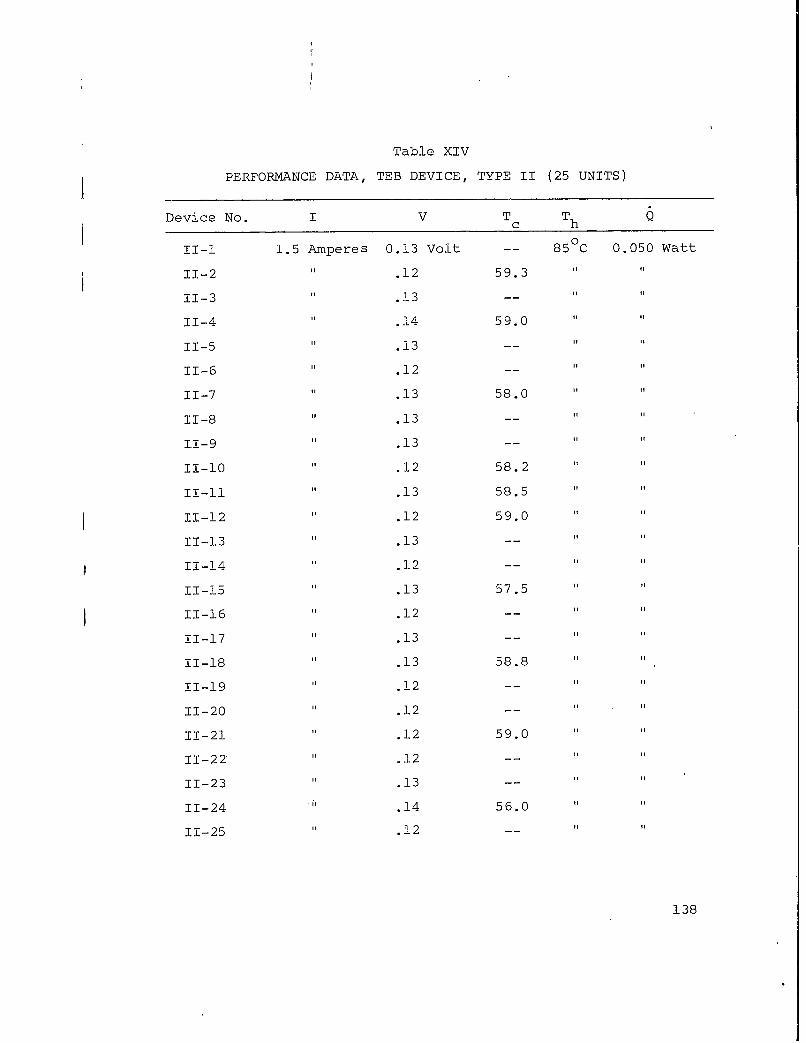
Table XIV
PERFORMANCE DATA, TEB DEVICE, TYPE II (25 UNITS)
Device No. I V T ThSc hIl-1 1.5 Amperes 0.13 Volt -- 850C 0.050 Watt
11-2 " .12 59.3
11-3 " .13 --
11-4 " .14 59.0
11-5 .13 -- "
11-6 .12 --
11-7 .13 58.0 "
11-8 .13 -- Ii
11-9 .13 -- "
11-10 .12 58.2
11-11 .13 58.5
11-12 .12 59.0
11-13 .13 -- "
11-14 .12 -- "
11-15 .13 57.5 "
11-16 .12 -- "
11-17 .13 -- "
11-18 .13 58.8
11-19 .12 -- "
11-20 .12 -- "
11-21 .12 59.0
11-22 .12 -- I'
11-23 .13 -- Ii
11-24 I .14 56.0
11-25 .12 --
138
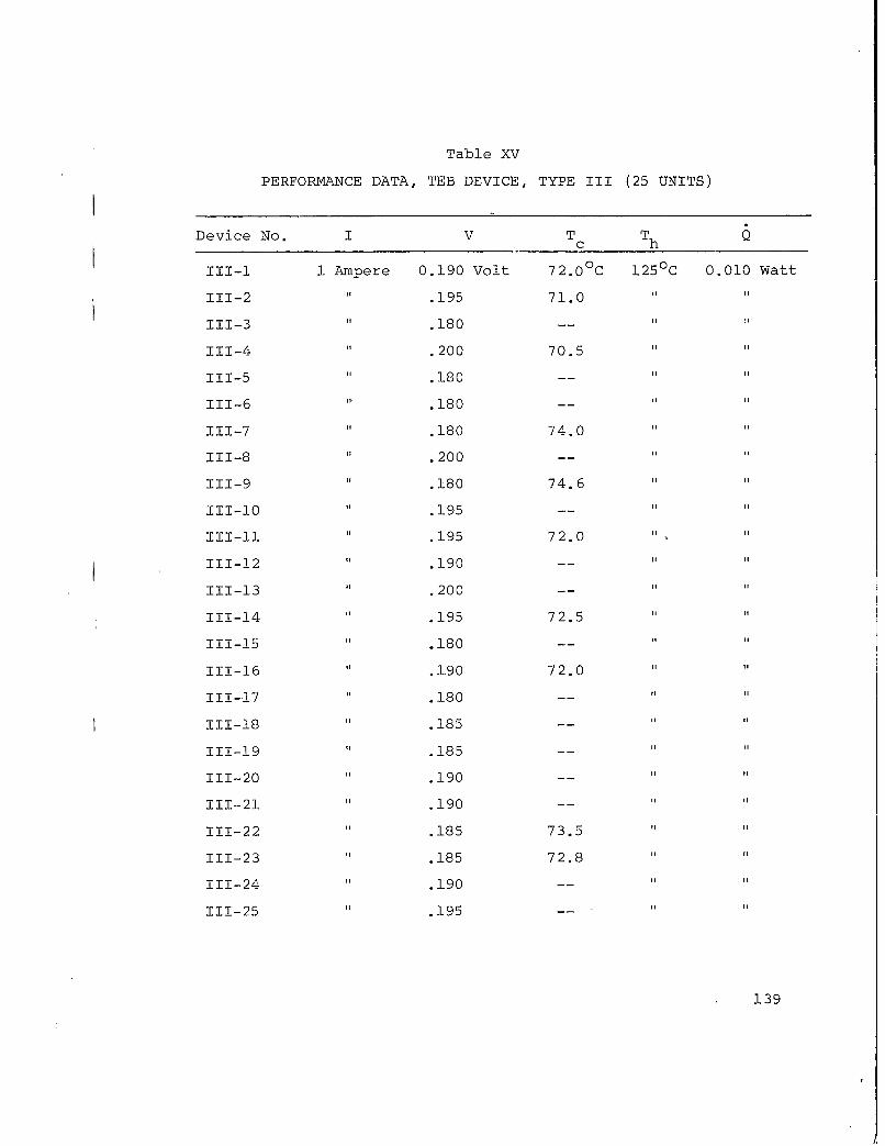
Table XV
PERFORMANCE DATA, TEB DEVICE, TYPE III (25 UNITS)
Device No. I V T T h
ch
111-i 1 Ampere 0.190 Volt 72.00 C 125°C 0.010 Watt
111-2 " .195 71.0 "
111-3 .180 --
111-4 .200 70.5
111-5 .180 --
III-6 .180 --
111-7 .180 74.0
111-8 " .200 -- I" "
111-9 .180 74 .6 ....
111-10 .195 -- i i
III-ll .195 72.0
111-12 .190 --
111-13 .200 -- " "
111-14 .195 72.5
111-15 .180 -- "
111-16 .190 72.0
111-17 .180 -- I" 1
111-18 .185 -- "
111-19 .185 --
111-20 .190 --
111-21 .190 --
111-22 i .185 73.5 "
111-23 .185 72.8 "
111-24 .190 -- "
111-25 .195 -- "
139
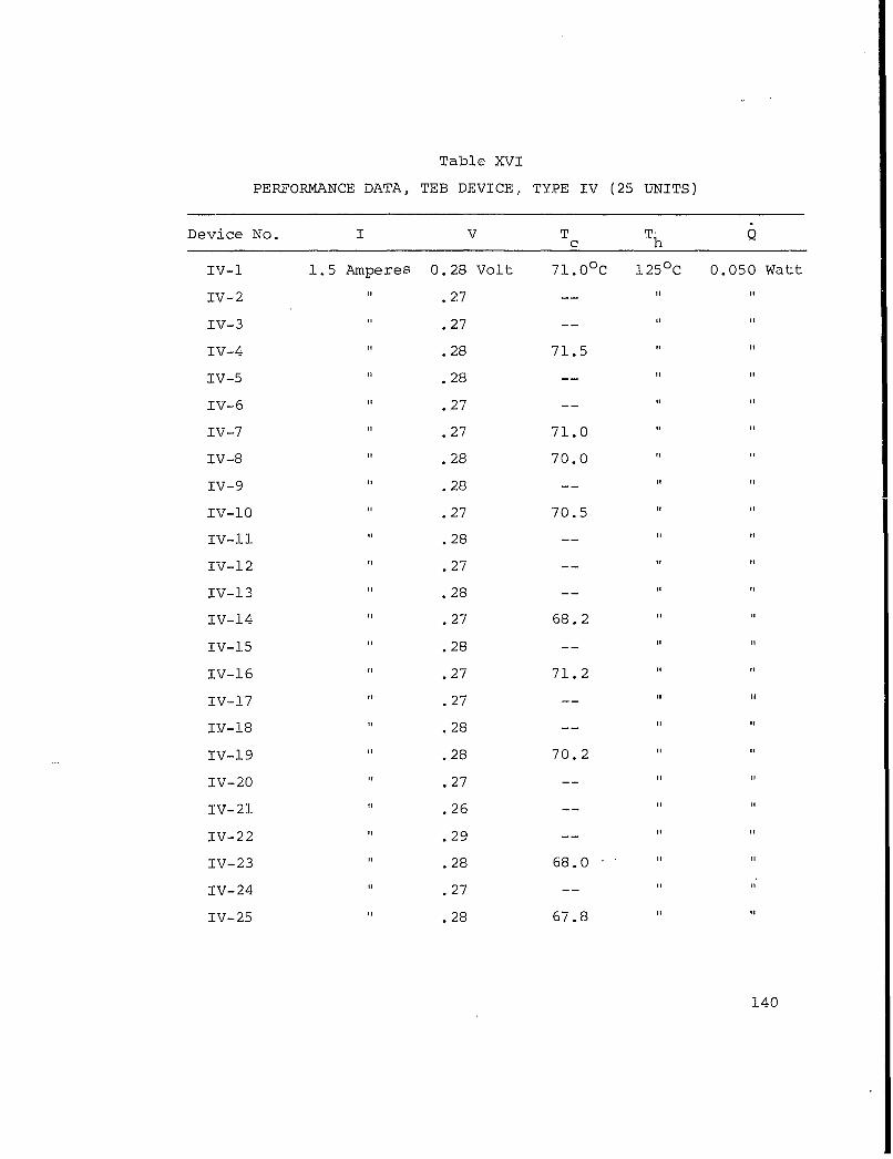
Table XVI
PERFORMANCE DATA, TEB DEVICE, TYPE IV (25 UNITS)
Device No. I V T TQ
ch
IV-I 1.5 Amperes 0.28 Volt 71.0°C 125 0 C 0.050 Watt
IV-2 " .27 -- "
IV-3 .27 -- "
IV-4 .28 71.5 "
IV-5 " .28 -- "
IV-6 .27 --
IV-7 .27 71.0
IV-8 .28 70.0
IV-9 .28 -- II
IV-10 .27 70.5
IV-11 .28 --
IV-12 .27 -- I
IV-13 .28 --
IV-14 .27 68.2
iv-15 .28 --
IV-16 .27 71.2
IV-17 . 27 -- II
IV-18 .28 -- It
IV-19 .28 70.2
IV-20 . 27 --
IV-21 .26 -- "
IV-22 .29 -- ".
IV-23 .28 68.0 I
IV-24 .27 --
IV-25 .28 67.8 It
140
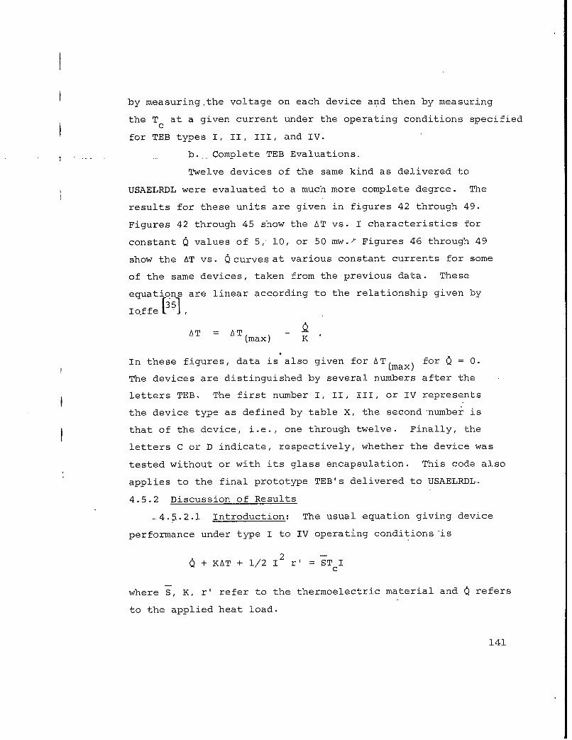
by measuring the voltage on each device and then by measuring
the T at a given current under the operating conditions specifiedc
for TEB types I, II, III, and IV.
b. Complete TEB Evaluations.
Twelve devices of the same kind as delivered to
USAELRDL were evaluated to a much more complete degree. The
results for these units are given in figures 42 through 49.
Figures 42 through 45 show the AT vs. I characteristics for
constant 0 values of 5, 10, or 50 mw.t Figures 46 through 49
show the AT vs. Qcurvesat various constant currents for some
of the same devices, taken from the previous data. These
equations are linear according to the relationship given by
IQffe•,
AT = AT(max) K
In these figures, data is also given for AT(max) for Q = 0.
The devices are distinguished by several numbers after the
letters TEB. The first number I, II, III, or IV represents
the device type as defined by table X, the second number is
that of the device, i.e., one through twelve. Finally, the
letters C or D indicate, respectively, whether the device was
tested without or with its glass encapsulation. This code also
applies to the final prototype TEB's delivered to USAELRDL.
4.5.2 Discussion of Results
.4.5.2.1 Introduction: The usual equation giving device
performance under type I to IV operating conditions is
2+ KAT + 1/2 1 r' = ST Ic
where S, K, r' refer to the thermoelectric material and Q refers
to the applied heat load.
141
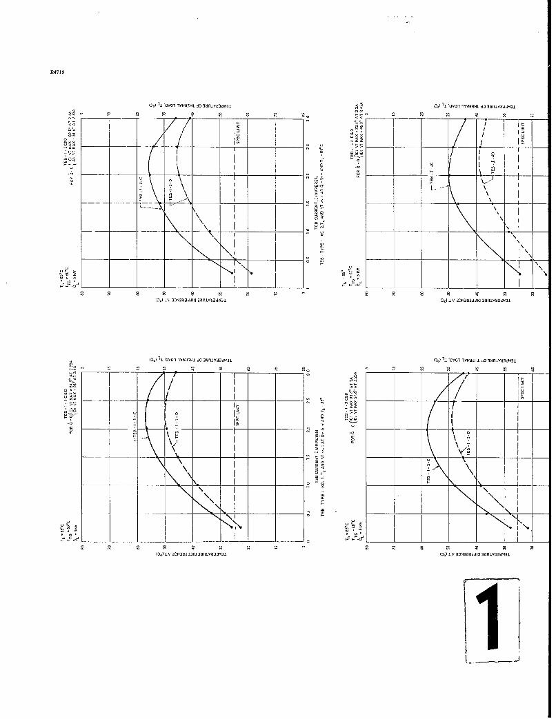
114719
'I� 1 0401144004130 01414000 'C 0. 0401 1V44'4 30 04014434001
.14 4 4 4 4 4 4 4 � 44 4 4 4 44 44��____ - _____
44 1�44 / I�I 0,
444- - - / 4 _____ ____ A _____
LI 44 1444 ----- -I----- 4 . .- -I----- -
4 4- 1I I I4�30 4 I4-.-, LI0 4 I
C 4 4 4
-- I 4 _'4 1'-\ 4 4
I 4.0 L-- I44 I
� � - - -4---- -
I 0 I4� I
_-,_ I 4 _
_____ I
U ------ 4LII, 4 4
0' -��,44 �< _______ ______ _______ _______ ______ L. _______ _______ .0
4 4 4 2 4 - 4 4 4 2 11 2(�) IV 0i0300332 04414443001 (DI) LV 0000403310 04414003401
4 � 1� '0401 140004130 0144034001%) �1 0401 1440001 40 04014004000
�o-<0< / - /44 / 4 /
___ ____ _________________ / [444 _______ _______ __________________________________IV
74� I44 . LI 4
*0 . I 10 4 -�
S -1-- -L' I
_____ -- I-- LI t
___ I - - '�--4-- -I - I
LI� LII 424 KL.0,20 I',. 44. 4 0�0* 44444 4.0
4 4 4 2 2 22 2 4 2 2 2 2
0%) LV 0000003310 04014434001 (DC) IV 0040403300 00014403001
1;
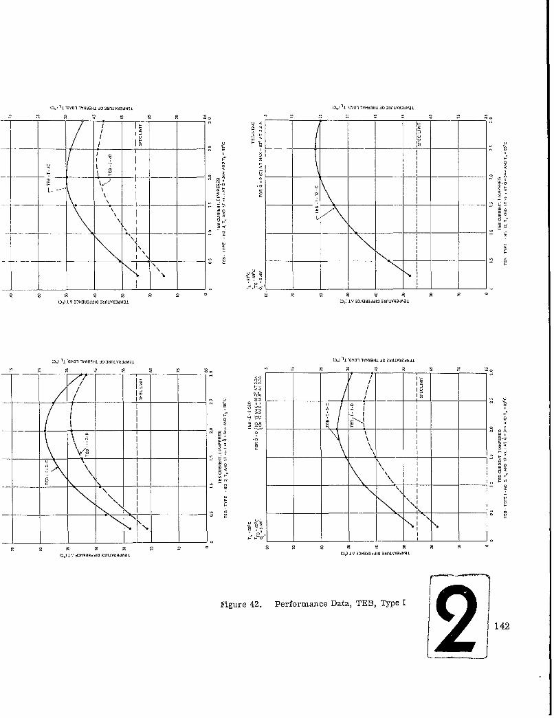
I 0001 1V00001 30 30010013001J�) I 0001100000130 H00i0003W�1
-- - - U 4 --
I -�4 I-T H (�jI 4
__ __ - - I H%
I - 0 -4 - 4I 04 I 0 < 40 01171 \\\< _ _ _ _ 44'O
I 4 oI 0.4
I 4 4_ __ _ __ __ __ __ __ I __ __ __ __ _
I - 4 03
___ _____ ____ _____ _____ _____ _____ _____ I _____ .� _____ _____ �1� _____ ____-
4 4 4 4 4 4 4 4(J0) IV 0J00003310 00010003001 (Jo) IV 0100003310 00010003401
)J& 1j '0001 100000). 30 00010033001 �0 �I '0001 1000001 30 0001000300j.4 4 4 4 4 4 4 4 4 4 4 4 4 4 4 4
4< jo.
/ I<4 I// I __ ____ U
0, �;-�- -- 4- 4 4
A -, A I__ I o 0v-s- -� -��--1----- 44 4 40
_____ - -i- 4� 4'- � - II I B<
o� 00.
- '.1 . ______ ______ -.- -4- - 4I II -
I 'I H
_ 44 _ _ _ - -� 44
I".. 0
4 4 4 4 4
IJ0) IV 3J00003310 00010003001 (JO) IV 0100003310 00010033001
Figure 42. Performance Data, TEE, Type I
142

13,709
(J' I 'OV<01 lYWH9HI JO BldnOyadWil '(~) 1 VO'l 1YW3H1 do f1v~dVd
II <<
' iviisH oanv dwi'I IVIIW3i4 a ~I K:W3
*~ I .
3:)NM3J10 3nlV~dM~ 0. IV3ON3344a 38i~ud" 0
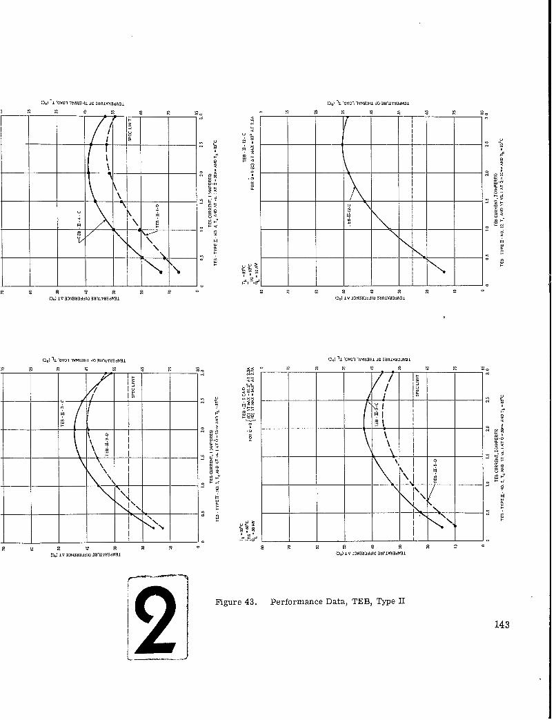
1) 1 'Ov1 lvwe3Hi adO fl1VdW21 ll '(1-~C- WldaHi 90 fl1YM&M
~ii U
2 2
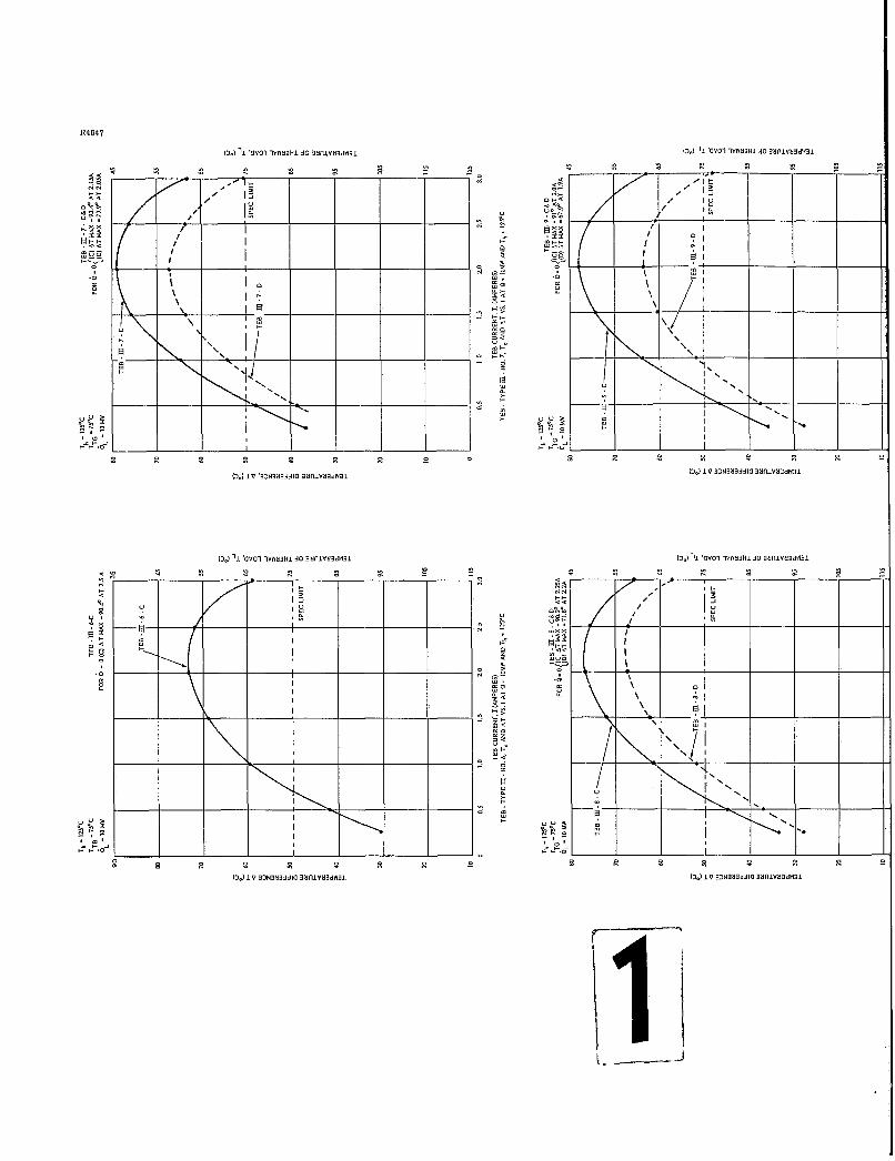
24647
11) �L '0401 10110461 dO 100146011 �I �1 4401 1610401 dO 40016117d1471
2 2 26 60. .1H
- 6 4- �.< / 10
/, - �40. /
0 /
/ I I022 I 00 I
I '.1 __ __
10 0
__ ___ - L ____ ___4 H0 0�
0 - 00
0 - 6S 0 I 'lx- xl I
IN.. I -�S 0 0I '. 0�0* 0.
N -I 6 N
6 -6 0- 006 N
I 00.,O�0 -.I 2.72 I
.7 �0; I I N 0� I I.OH 4 I .0 H 4 I
- - *.*j ______ L _____ J 00.0 _____ ______ ______ ± _____ ______2
2 2 2 0 2 0 0
1%) IV 0DNl4lddIO OIOIIIVOI0dVI0IIIO) IV NO0lddI0 0001V04dII0i.
01 1j. '0401 14603101 dO fl1002d63I 2�I �I '0401 1V604I0i 30 flIVOOdlOOl
<0 0 0 2 2
- 00 H6 HH
0 064______ 0 / 0
0 - 000
0 66
6 -� I.0 -� � 40 0 I
0. 0!
_ 0 il�Ž14 �- 0,01
o H
____ N/i ____H'.6 - -N
N N
N N
- 0 N
o �2� I -N- 006 0 N
- - - I - I* ON * ON.004 .00.4- H -0 H H .0 _______________
00 � 2 2 2 2 2 2 2 g 2ID�) IV ODN004diI0 0801YlIOdWOJ. ID0! IV 0DNO03ddIO 00016006101
'�0,
jK
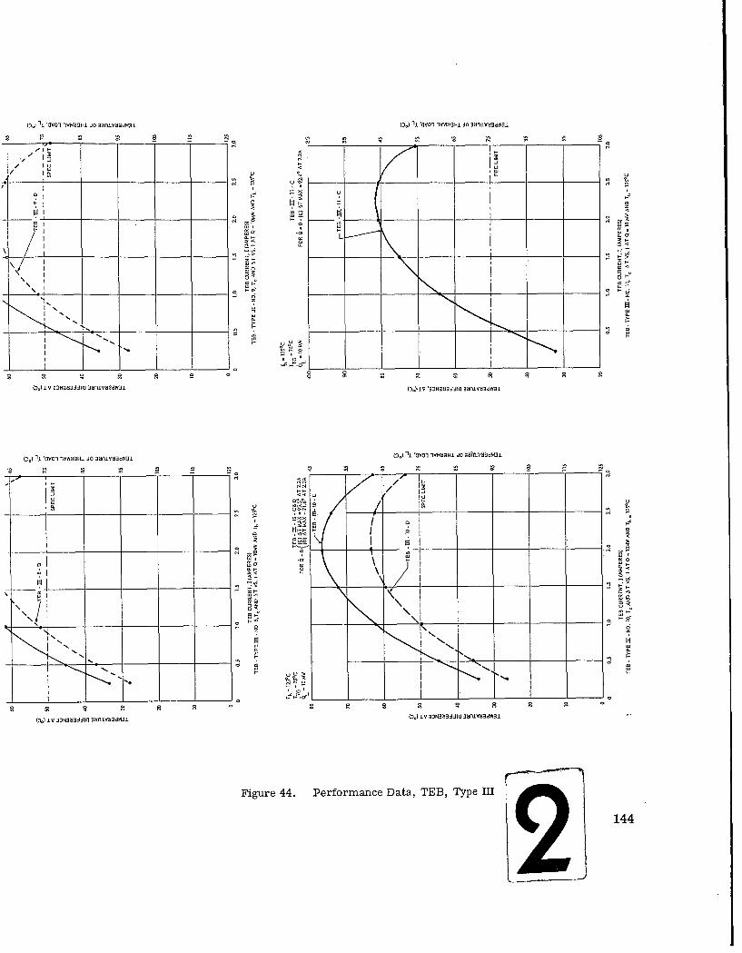
%4 1i. 0001 1004004{[ �0 0001V�0dW0i. 4J0) �1 OVOl 1V4444�4U �0 VOOIVOOdV4HI
0 0 -�- - - 0 _______ _______ - _______ - 0
"I 4- 0 1 K-- I
/ I� U I U
I U -
0 I C0 o
____ 0 ____ 0* 1 0
00
01 - 0�.
00 00____ I
' -� _____ 0 -g'Is 0 I
H4 S
0.N -
-i -
F o o -
I N 0
0* 00
_______________ _______________ _______________ ______________ _______________ ______________ _______________ _______________ _______________ ______________ j _______________ _______________ ______________
_______________ I _______________ _______________ ______________ _______________ ______________ _______________ _______________ _______________ ______________ _______________ _______________ ______________
0 * 0 � o
41410 00lJH�i�I0 fl10�0�4'�J. 4141000440,4,00 010440d440.L
41) �J. '00011000044100 000100004001 (14 �1 '00011400401 40 AVOOdWOl.0 0 0
H
0 .0<
I 0I ___ ___
0 0 ___ ____
01 �0 0 00
0 o-� 04 00 '±- 0�
" Ii
0, -0
N
I "N
-NN
____ 0.0 ____ ____ ____ I ____ ____ ____
0 0 - 0 0
41110 044000010 00010000440i. 41410 441000004i0 40o010004W01
Figi.ire 44. Performance Data, TEB, Type m'44
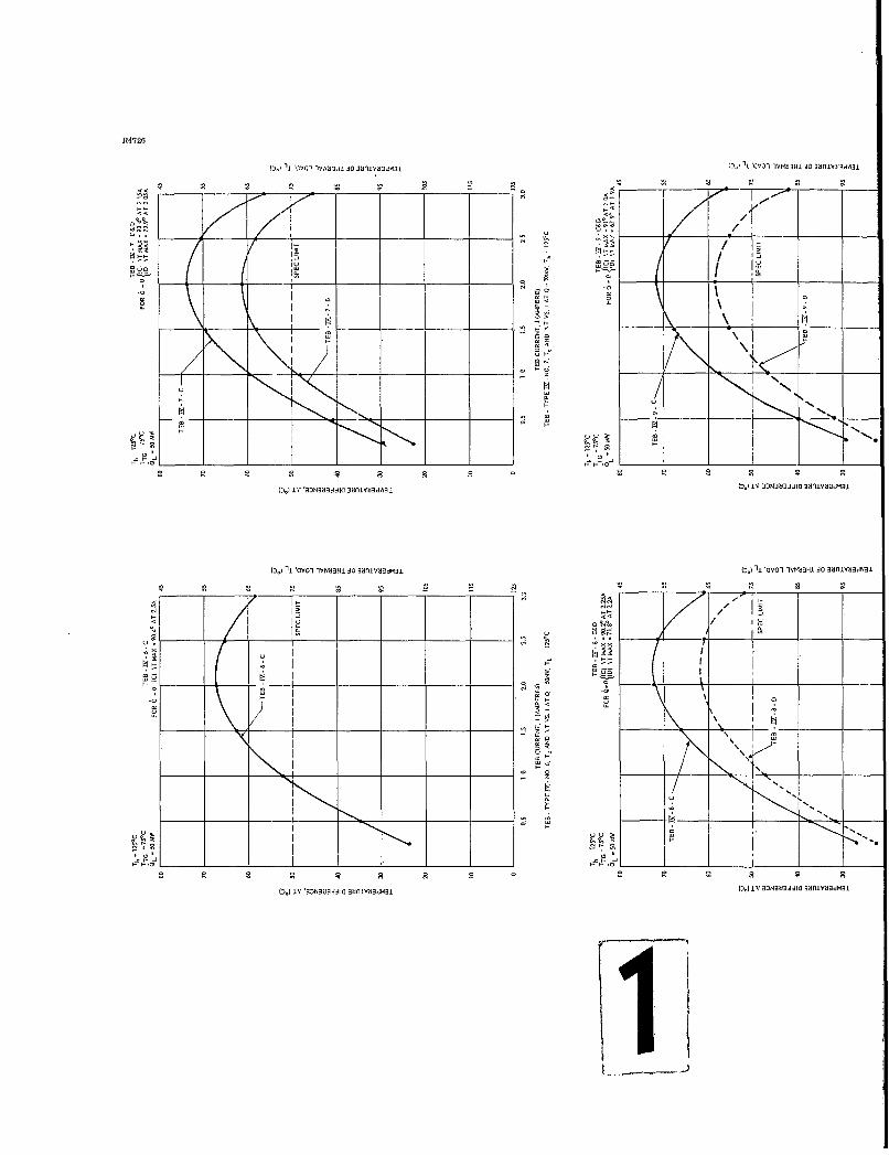
R~4726
IV' 'aNaAGa0imdG IV OMJG3nV~W9
(0)11 '0<01 I000001 ,10 0001080d00 0W 1 1 000001VW3H jo 3snVN0dW3I
/7 I
O 00
IV 03NU3~( 0MVUB 3'Na0di MMI
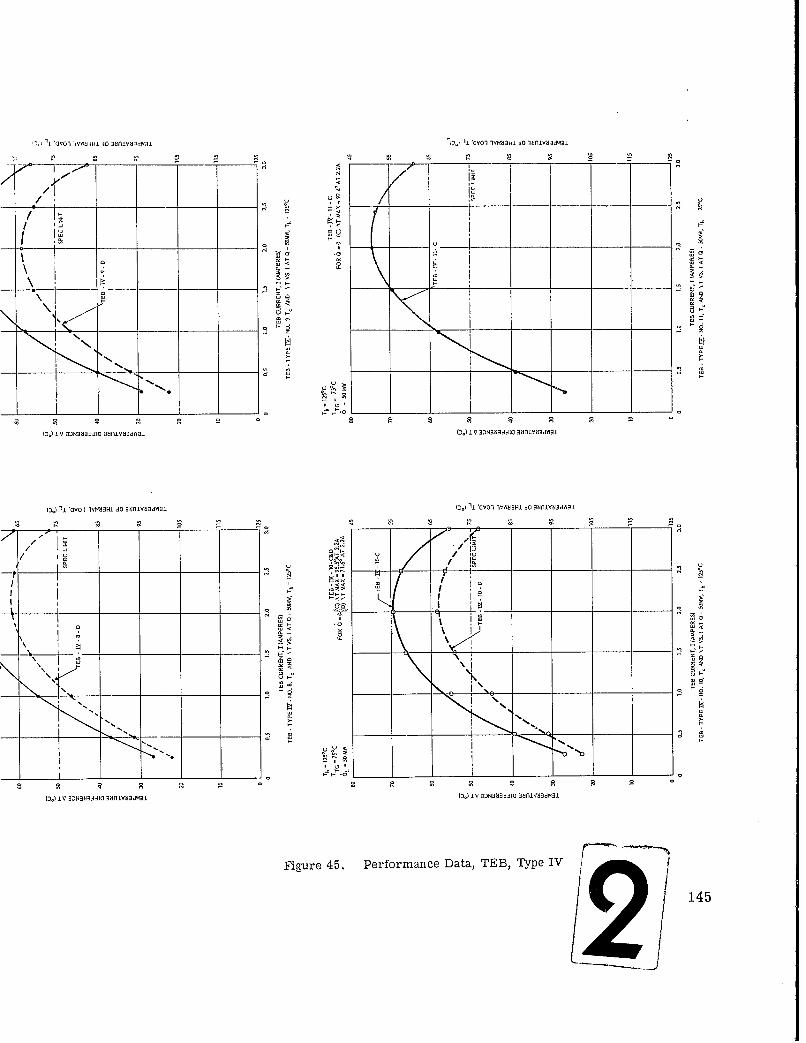
ýD J1 '0001 000 -1Yd~4 0 3000000000j 'I 0001 IV01al8,. JO flIY83dWai
.7 y
N N
C!. 0
010
(3.) 1
V ON38 AAla 10131 8O 00000300 B~o dO. 0I0 IV 00 3N 10 38 01003dW 01
Fi u e4 . P ro m n e D t ,T B y eI 4
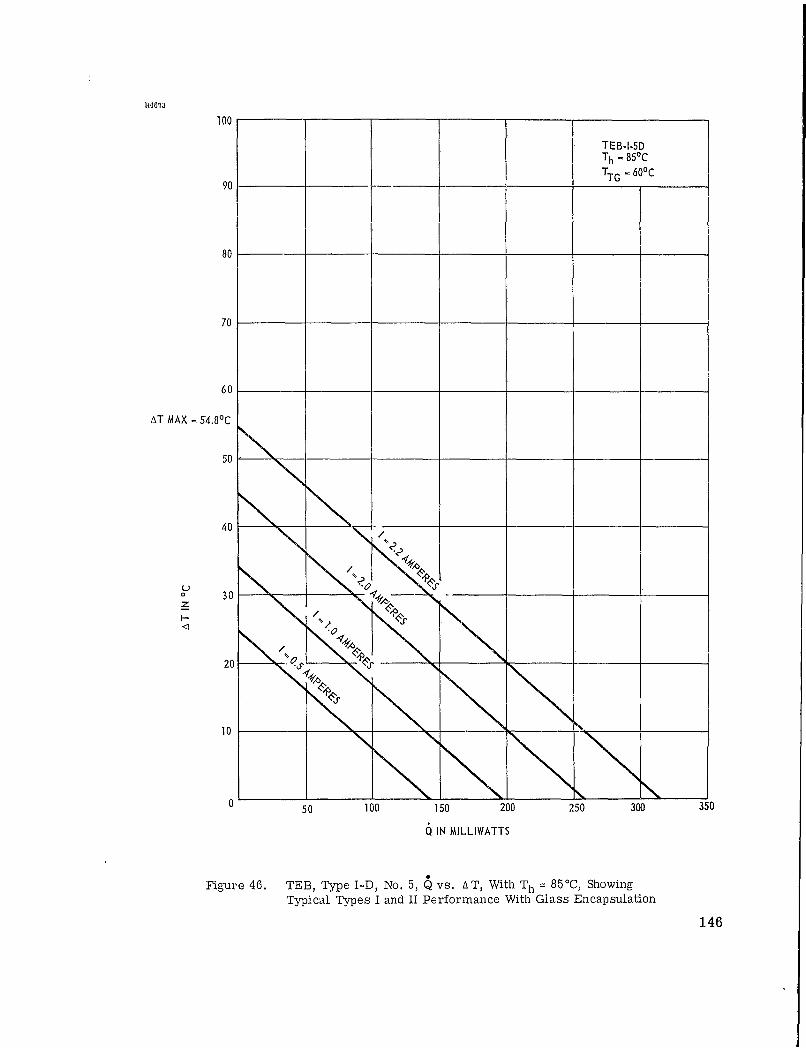
R4673
100
TEB--51DTh - 85'C
90- TTG - 600C
80
70
60
AT MAX = 54.8 0C
50
40
U .0 __ ___3 30o1-
2Oe
10
50 100 150 200 250 300 350
Q IN MILLIWATTS
Figure 46. TEB, Type I-D, No. 5, Q vs. AT, With Th = 85°C, ShowingTypical Types I and II Performance With Glass Encapsulation
146

R4682
100TEB-I-5CTh - 85oC
TTG - 60'C
90
AT MAX - 81.2 0 C
80
70
60
50
4 4 0
30
S4o
200
10
0050 100 150 200 250 300 350
Q IN MILLIWATTS
Figure 47. TEB, Type I-C, No. 5, Q vs.. 6T, With Th = 85 0C, Showing
Typical Types I and II Performance Without Glass Encapsulation
147
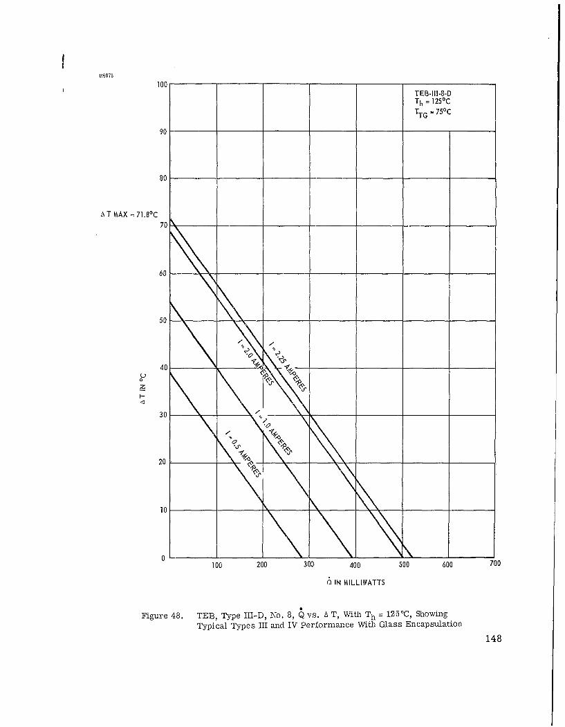
R4675
100TEB-I1I-8-DTh = 125°C
TTG - 75°C
90
80
A T MAX =71.80 C70
60
50
40U0z
30
20__ __ _
10
0100 200 300 400 500 600 700
SIN MILLIWATTS
Figure 48. TEB, Type III-D, No. 8, Q vs. A T, With Th = 1251C, Showing
Typical Types III and IV Performance With Glass Encapsulation
148
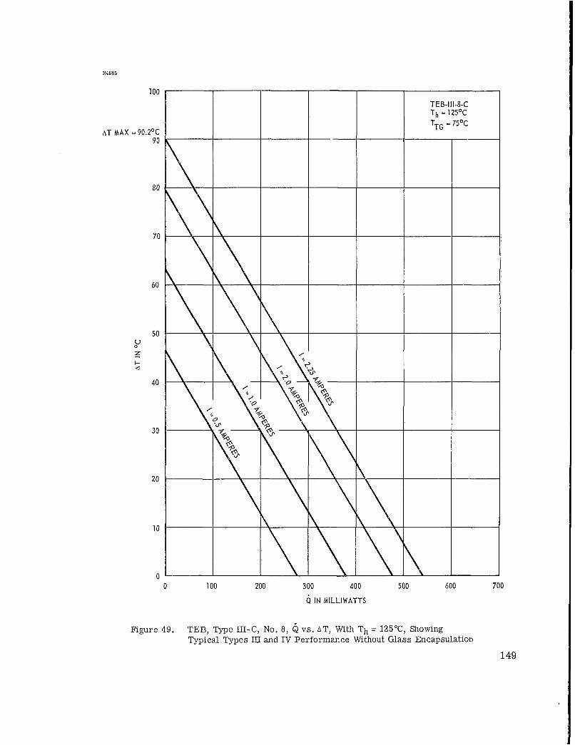
R4685
100TEB-III-8-CTh = 125°C
AT MAX = 90.2 0 C TTG 75oc90
80 ______
70
60 _____
50C
P%40
% 0
0100 200 300 400 500 600 700
6 IN MILLIWATTS
Figure 49. TEB, Type III-C, No. 8, Qvs. 6T, With Th 125'C, ShowingTypical Types III and IV Performance Without Glass EncapsulatioD
149
The left side of this equation represents the heat flowing
into the cold junction, while the right side represents the
heat flowing out of the cold junction because of Peltier heat
absorption. This theoretical equation neglects two correction
r and(insulation)' which should be included on the
left side of the equation.
2 -
Qt = + Qr (insulation) + K(Th c+ 1/2 c r' ST I
or
2 -t 0 + + K + K(insulation) (T - Tc) + 1/2 I r'=ST I
(1) r is the heat transferred by radiation exchange
between Th and Tc through the nonthermoelectric parts of the
heat exchange area r. 0 and K are given byr r
4 4•r= C('lF1T -h T2C ) and K Qr/(Th - Tc)
where T1 and u2 are the emissivities of the surfaces at Th and
T respectively and K is the effective thermal conductancec r
attributable to the radiation flux.
(2) Q(insulation) is the heat conducted through the glass
encapsulation (and air if the TEB device is tested or used in air).
Q(insulation) K (insulation) AT
Kk (insulation)A'
(insulation) L
The terms Q(insulation) and K(insulation) are further defined in
the glossary.
150
Taking these excess heat fluxes Qr (insulation) and
their associated thermal conductances K and Kr (insulation)
into account, we can calculate the effective figure of merit
,Z", of the device from:
(r + rc) (K + Kr + K (insulation)
zr K +K.
(+ c) (1+ r (insulation))r K
where the materials figure of merit
-2 --2S SZ = -r K p k
4.5.2.2 Comparison of Experimental and Theoretical
Performance: The data for the interim devices given in figure
39 may be checked against theory. Assuming the device Z" =- 30 -1 - o - -3 -
2.5 x 10 (°K)-, (S = 440 pLv/ C, p = 10 ohm-cm,pc = 10
2 -3 0ohm-cm , K = 3.52 x 10 watts/ K), the calculated theoretical
values (see figure 4) shown in figure 39 by the points indi-
cated by 'x' indicate reasonable theoretical agreement.
The theoretical agreement for the data presented for the
twelve final prototype TEB's under type I, II, III, and IV
conditions (table X) is also reasonable, as may be seen from
figures 50 to 57. These curves represent plots of average and
extreme values of AT from the data presented in figures 42
to 45, inclusive, for type I to IV devices without glass encap-
sulation (C), and with glass encapsulation (D). The theoretical
current values for Z" = 2.5 x 10⁻³ ( K)- which should give the
151
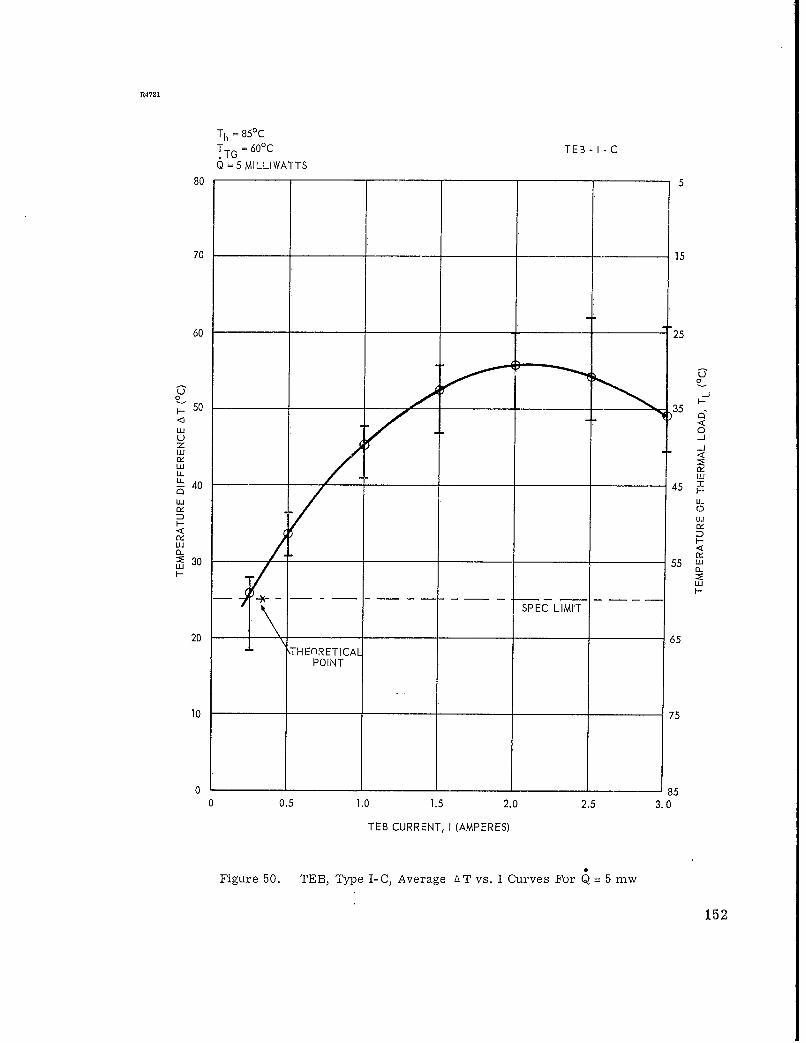
R4721
Th = 85°CTTG = 600C TEB - I - CQ =5 MILLI WATTS
80 5
70 15
60 25
. 50 35
"w 0ozu
U- .Lu. 40
45_._-
uJ u
-<-
tu .i
: 30 55
20 ~SPEC LIMIT 620 ]65
"" THEnRETICALPOINT
10 75
0 850 0.5 1.0 1.5 2.0 2.5 3.0
TEB CURRENT, I (AMPERES)
Figure 50. TEB, Type I-C, Average AT vs. I Curves For Q = 5 mw
152
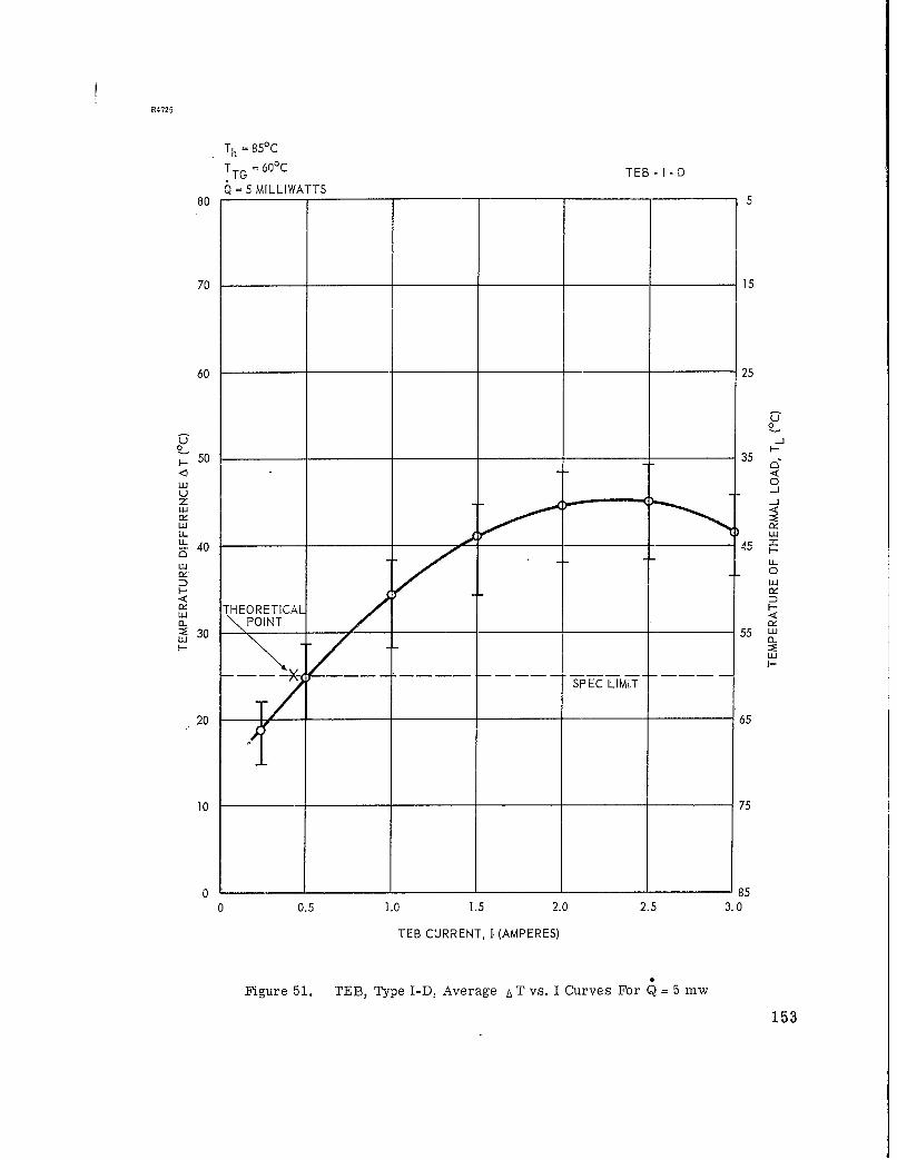
R4725
Th = 850C
TTG = 60 0 C TEB - I- D
Q = 5 MILLIWATTS80 5
70 15
60 25
00
S50 35 •
LU 0U -Jo "Hz
LL 4o 5IL UJ
__ __THEORETICAL_
C \xPOINT o::
SPEC LIMIT
20 65
10 75
0 85
0 0.5 1.0 1.5 2.0 2.5 3.0
TEB CURRENT, I (AMPERES)
Figure 51. TEB, TIype I-D, Average A T vs. I Curves For Q=5 mw
153
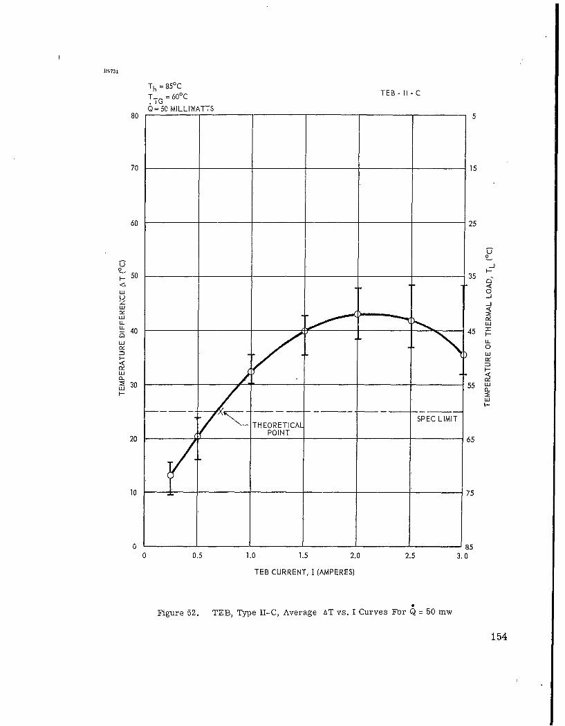
R4731
Th = 850CTTG = 600C TEB -Il-C
Q 50 MILLIWATTS
70 15
60 25
00o Io
wU 0U
UjIx
U -. _4. 40 5 H
wU U-0ý 0
w0ý
- 30 45 x.-_
w.
-- SPE LIMI
- ___ - 7IITHEORETICAL
10 75
0 850 0.5 1.0 1.5 2.0 2.5 3.0
TEB CURRENT, I (AMPERES)
Figure 52. TEB, Type II-C, Average AT vs. I Curves For Q = 50 mw
154
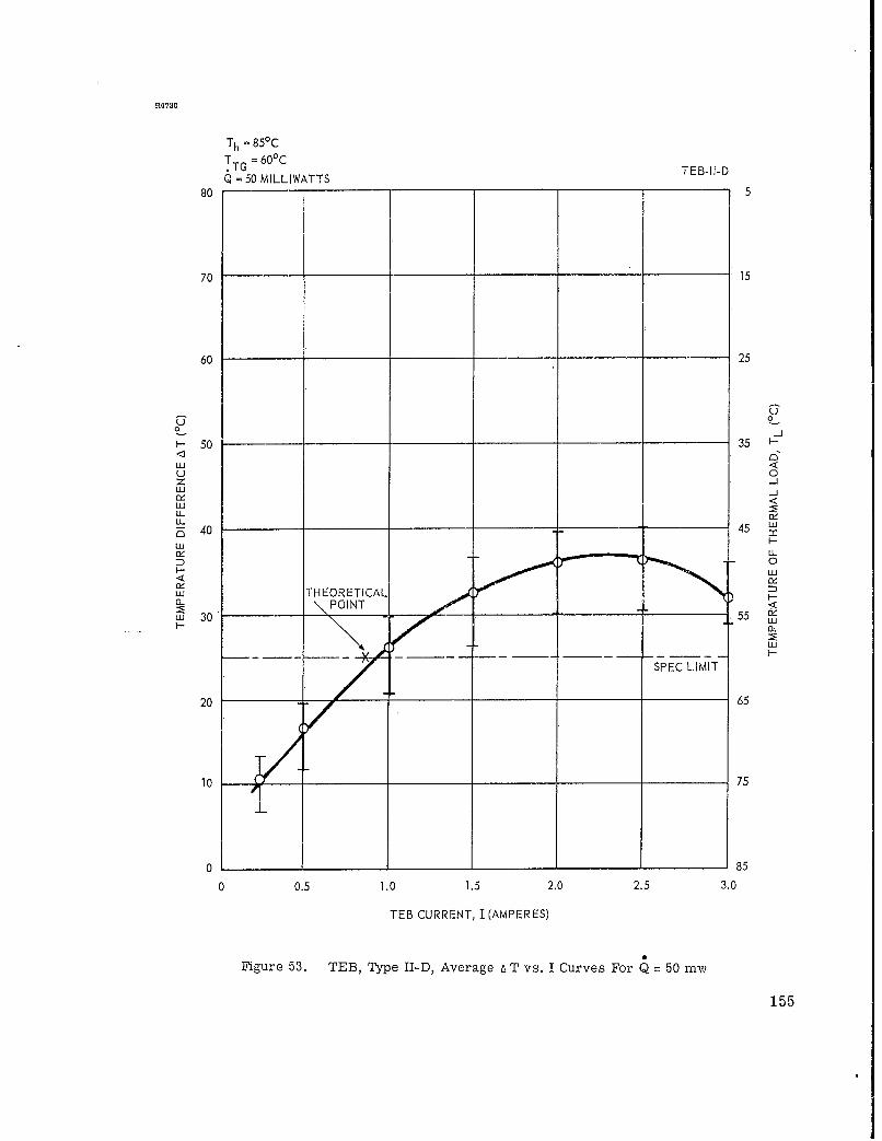
R4730
Th = 850CTTG = 600 C TEB-11-DQ =50 MILLIWATTS
80
70 15
60 25
Go
- 50 35
u 0zLU .wrv <
U-U-5 40 45
............. LLD 0F- - L•
H
-, THEORETICAL.30 _POINT <__-"'U 30 -55 C)-u
ILILU-
20 ~SPEC LIMIT 620 65
10 75
0 185
0 0.5 1.0 1.5 2.0 2.5 3.0
TEB CURRENT, I(AMPERES)
Figure 53. TEB, Type II-D, Average A T vs. I Curves For Q = 50 my,,
155
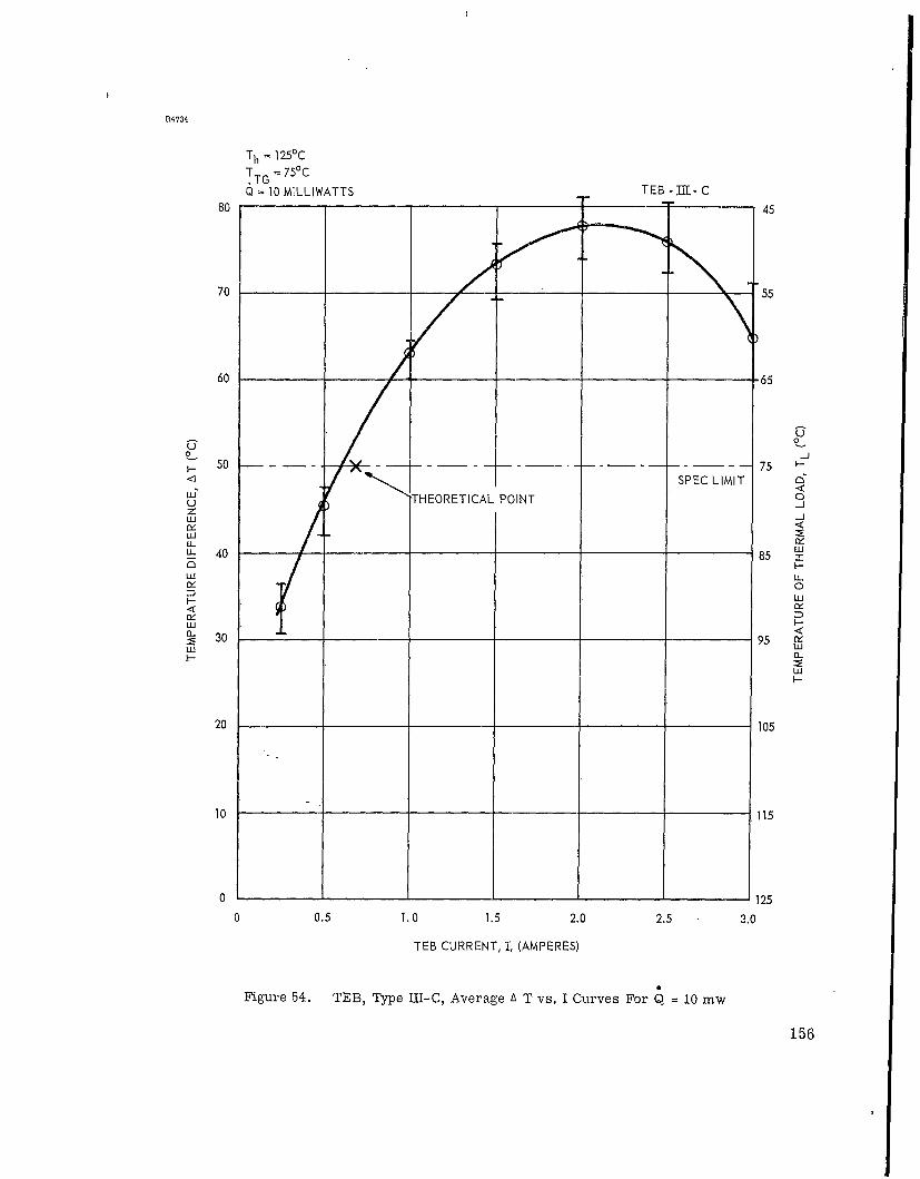
R4734
Th = 125'CTTG = 750C
Q 10 MILLIWATTS TEB -]I[- C80 45
70 55
60 65
0 S50 75 •-SPEC LIMIT
LU THEORETICAL POINT 0zu.LUU..u!. 40 85 W
LU UL.0
D LI- 3.:
Lu I-
0 3 _95 ctLU ULUL
1-
20 105
10 115
0 1250 0.5 1.0 1.5 2.0 2.5 3.0
TEB CURRENT, L (AMPERES)
Figure 54. TEB, Type IJI-C, Average A T vs. I Curves For Q = 10 mw
156
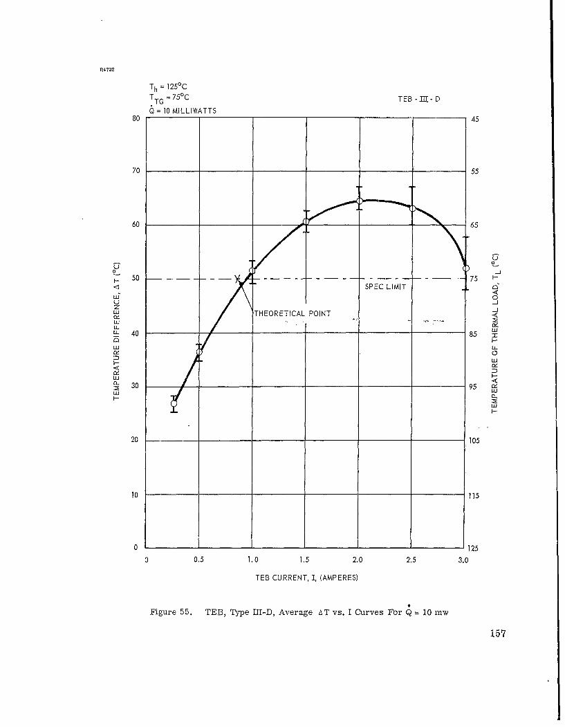
R4732
Th = 125 0 CTTG = 750 C TEB -TIT- D
Q = 10 MILLIWATTS80 -45
70 55
60 65
50s • 75<1 SPEC LIMIT •
U-
00I-i
<1a <U j
w THEORETICAL POINT¢vulLL 4
1_ 0 115 .-
30 125 w
00.5 1.0 1.5 2.0 25 3.0
TEB CURRENT, I, (AMPERES)
Figure 55. TEB, Type III-D, Average AT vs. I Curves For Q oI mw
157
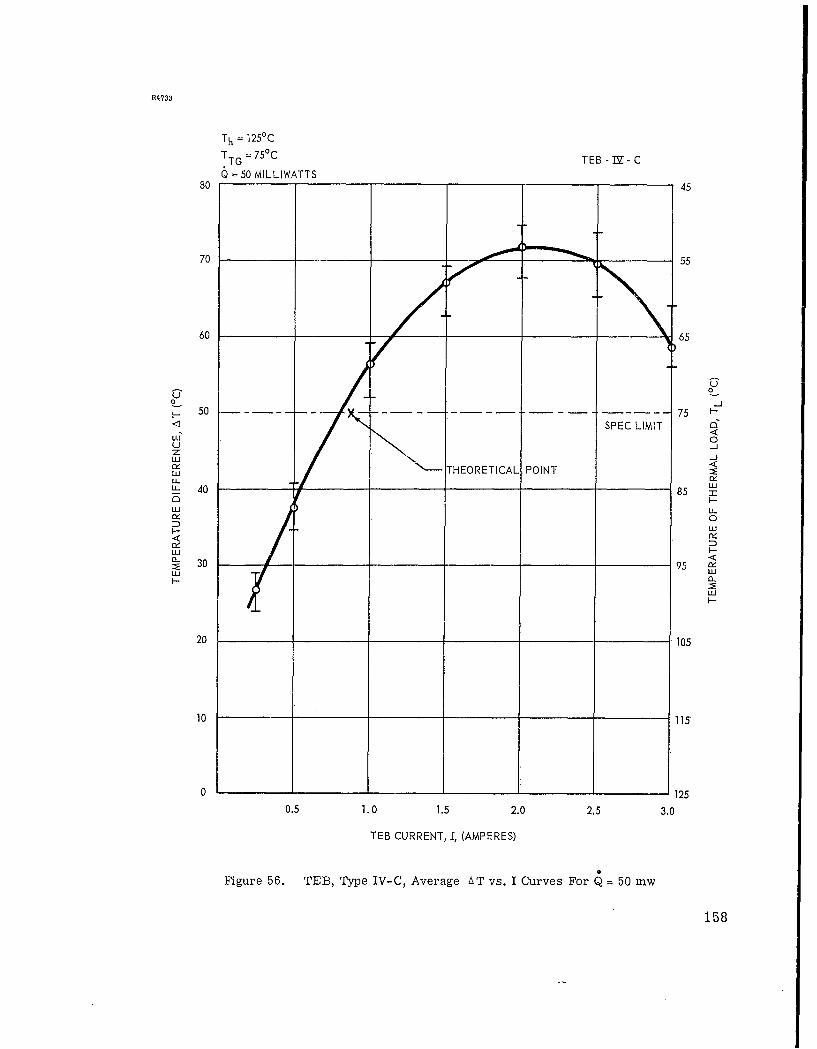
R4733
Th = 125 0C
TTG = 750 C TEB -IV- C
Q =50 MILLIWATTS80 45
70 - 55
60 65
0 S50 . . . .. 75
<•; SPEC LIMIT
LdUZ
THEORETICAL POINTLuU-!L- 40 78
Lu U..0Lu.<
L <:: 30 95 w-
wLui a--
20 105
10 115
01 125
0.5 1.0 1.5 2.0 2.5 3.0
TEB CURRENT, I, (AMPERES)
Figure 56. TEB, Type IV-C, Average AT vs. I Curves For Q = 50 mnw
158
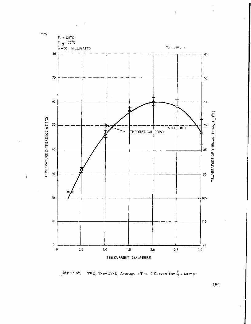
R4729
Th = 125 0 CTTG = 750 C
Q=50 MILLIWATTS TEB -IT- D
80 45
70 S5
60 -65
u .-J
S50 75SPEC Lo<
w 0THEORETICAL POINTzi
Li :c
I--<I-
Ujwu 30 950mLUI-.
20 105
10 115
0 -125
0 0.5 1.0 1.5 2.0 2.5 3.0
TEB CURRENT, I (AMPERES)
Figure 57. TEB, Type IV-D, Average • T vs. I Curves For Q = 50 mw
159
desired type I through IV performance are plotted on the curves
for devices without glass encapsulation by points designated
by 'x' o (See table XI.) Agreement between the theoretical
and experimental currents at the operating points indicated
by table X is satisfactory. It would thus seem that the
behavior of the TEB device can be represented by device figure-3 o -l1
of merit of Z" = 2.5 x 10 ( K) The parameters of the
thermoelectric material measured by the Z-meter technique gave-3 o -l1
a materials figure of merit Z of 2.83 x 10 ( K) The
difference between Z" and Z may be explained by the discussion
and equations in 4.5.2.1. Using the equations in that section,
Sr 4.9 mw for type III and IV conditions. This value wasr
calculated assuming that the average emissivity associated with
Th = 125 0 C is _i • 0.30 and the average emissivity associated
with T =' 75 C is T2 G 0.44. The surface at T consists of
partially oxidized copper. The handbook emissivity values for
the emissivity for a pure copper surface iss -- 0.1, but for
copper oxide it is 0.6. Assuming the surface at T is approxi-c
mately 90% oxidized, the selected value of -2 is obtained.
The surface at Th is partly alumina (s a 0.2) and partially
oxidized copper. Using the known proportions of partially
oxidized copper and alumina, an approximate average value of
0.3 for the emissivity of the surface at Th was estimated.
Thus, the correction terms p and Q are such as to account
adequately for the difference between the measured materials
figure of merit, Z and Z".watts
Using the value of 0.0076 cmatK for the thermal con-
ductivity of glass, the Z" for the glass encapsulated modules
is calculated as explained in 4.5.2.1 with the result
160
-30 -lZ1 - 2.1 x 10- ( K)- , using the calculated values for 0(insulation)
and Q for type I to IV conditions. The approximate calculatedr
heat flow, Q(insulatio•,for values of Th =85°C and Tc 60 C
(types I and II) is 16 mw and for Th = 125 0 C and T = 75 0 C
(types III and IV), Q(insulation) is 32 mw. The theoretically
calculated values for AT under type I to IV conditions are given
by the theoretical point (x) on the curves of figures 51, 53,
55, and 57. The agreement between theory and experiment is
good. The important effect of the glass encapsulation is
clearly shown by comparing the C and D curves in figures 50
to 57.
161
5. CONCLUSIONS
The TEB device requirements defined in USAELRDL Technical
Requirements SCL-7635 and summarized in table X have been met
with currents considerably less than the three amperes specified
as the upper limit. The average current, as shown in figures
50 to 57 for type I, II, III, and IV operation without glass
encapsulation, was 0.25, 0.7, 0.6, and 0.8 amps, respectively.
With glass encapsulation, the corresponding average currents
were 0.5, 0.95, 0.92, and 1.17 amps. Thus, the method of encapsu-
lation is of critical importance. The theoretical curves of
figures 3 and 4 indicate that, for operation at C.O.P. (max)'
(max)' and the crossover point between them, currents of 1.3,
3.5, and 2.1 amps, respectively, are required. It is thus
apparent that the TEB devices constructed will operate at
greater C.O.P. for higher heat loads than those specified by
type I to IV conditions. This point was emphasized in para-
graph 4.3.2, on design calculations, where the limiting factor
was the technological limit to the area of cross section of
the thermoelectric legs attainable.
No unusual difficulties were encountered in manufacturing
25 units of each type (I to IV) called for by SCL-7635, but
the development of semiautomatic methods will be important for
quantity production.
Worthwhile improvements could be used in TEB device per-
formance, which may be achieved principally by reducing radiation
heat leakage and heat leak through the glass encapsulation.
The device performance was limited by technological limits
placed on the TEB device height. A higher C.O.P. could have
been achieved under the specified heat loads only by advances
162
in the state of the art of producing thermoelectric legs of
smaller cross-sectional area, as explained in paragraph 4.3.2.
This cross-sectional area was limited by the present technology,
which could be extended to reduce this area by a factor of
between approximately 5 and 10 times. As shown in figures 3
and 4, considerable excess pumping capacity has been introduced
into the devices, and operation at higher heat loads and currents
would result in operation in the most favorable region between
CO (ma and Q(max)' It is expected that this extra heat-
pumping capacity available at currents less than 3 amps will
be of value in the practical applications of TEB devices to the
temperature control of temperature-critical electronic components.
163

6. RECOMMENDATIONS
Although the devices developed in the present contract
easily meet the specified type I to IV operational requirements,
several worthwhile improvements can be made. These improve-
ments are discussed below.
6.1 Improvements Related to the Present Device Configurations
These include:
a. Improved encapsulation procedures to make the fabri-
cation process less time consuming and to reduce thermal con-
duction through the encapsulation.
b. Emissivity control to reduce the radiation flux through
the spaces not occupied by thermoelectric material. For instance,
the surfaces at Tc and Th could be plated to have as low an
emissivity as possible.
c. A thorough experimental device analysis should be
conducted on one device of each type to check the theoretical
predictions of figures 3 and 4 together with extensions to
higher heat loads and additional temperatures.
d. Extensive life tests should also be performed on TEB
devices under operational conditions.
6.2 Improvement in Configurational and Thermal Design
These include development work to:
a. Reduce the height of TEB devices to one-half, or less,
their present values so that the devices can be fitted into a
smaller space.
b. Extend the TEB devices for operation at higher heat
loads (1 watt, or higher), using the design criteria for minimum
current and higher voltage of operation. This may be achieved
by using 16 or more legs of reduced cross-sectional area.
164
c. Improve the heat-transfer characteristics and simplify
fabrication procedures using thermoelectric legs integrated with
BeO ceramic micromodule wafers of high thermal conductance and
high electrical resistance. The electrical conduction paths
could be formed by various methods, -,ich as metal plating and
selective etching.
6.3 Additional Cooling Design Concepts
These include;
a. The direct integration of thermoelectric cooling legs
into the temperature-sensitive device. Thus, a temperature-
sensitive transistor could be mounted onto a Be0 micromodule
wafer and the thermoelectric cooling legs connected directly
to the transistor mounting wafer. Alternatively, the thermo-
electric legs could be incorporated directly into the transistor
can. These procedures would have the advantage of enabling
a precise matching of the thermoelectric TEE design to the
specific cooling requirements of a specific temperature-
sensitive component.
b. Thermoelectrically cooling a whole micromodule stack
instead of a specific component.
C. Thermoelectrically cooling a complete chassis instead
of an individual component or module stack by thermoelectrically
cooled and dehumidified air.
It is anticipated that all four approaches to solid-state
electronic cooling (that is, the TEB micromodule approach, the
matched individual specific component approach, the micromodule
stack approach, and the thermoelectric cooling of the chassis
by dry thermoelectrically cooled air) will have certain advan-
tageous areas of application.
165

7. IDENTIFICATION OF KEY TECHNICAL PERSONNEL
During the period of this contract, the following key
personnel participated in the work discussed in this report.
7.1 Man-Hours Expended
Name Title Man-Hours
Nicholas Fuschillo Head, Solid-State Physics 150Section
,
Paul A. Mullin Physicist 200
F. Kent Eggleston Principal Engineer 300**
Forest K. Luckett Solid-State Technician 600
Orville B. Van Blaricon Design Engineer 150
Eugene B. Stewart Senior Thermoelectric 60Technician
Total 1,460
7.2 Personnel Resume"s
Resumes of the key personnel assigned to this project
follow:
,
Mr. Mullin replaced Mr. John D. Boardman on this program;the latter was called into the U.S. Air Force.
**
Mr. Luckett was transferred to this program after thedeparture of Mr. Stewart.
Mr. Stewart left Melpar in June 1962.
166
Nicholas Fuschillo received B.S. and M.S. degrees in physics
at the University of London, he presented a dissertation on
the control and measurement of temperatures from the lowest
to the highest attainable. He received a Ph.D. degree in 1952
at the University of Leeds, where he studied with E. C. Stoner
and F. E. Hoare. There, he worked in the low-temperature
laboratory and did thesis research on thermoelectric effects
in liquid and solid metals and alloys, as well as on precision
low-temperature gas and thermoelectric thermometry. He con-
tinued research in the Department of Engineering Physics at
Cornell University, where he studied the mechanical properties
and audiofrequency attenuation in metallic single crystals
from 20 to 400 0K.
In 1954, Dr. Fuschillo was appointed assistant professor
of physics at Pennsylvania State University, where he taught
classical mechanics and solid-state physics at the first-year
graduate and senior undergraduate levels, as well as second-
year courses in atomic and nuclear physics, electricity, magne-
tism, and thermodynamics. His research activities were
principally in nuclear magnetic resonance as applied to the
study of surfaces, radiation damage, molecular diffusion, and
rotation, as well as in the thermal and mechanical properties
of high polymers, molecular crystals, and molecular radiation
damage.
Dr. Fuschillo went -to the Franklin Institute of the State
of Pennsylvania in 1957 as the head of the Magnetics and Semi-
conductors Branch. In addition 'to directing the Institute's
industrial co-operative programs in thermoelectricity and fine-
particle magnetics, he initiated and supervised research programs
167
for the government in superconducting and semiconductor r-f
thermal detectors as well as organic and plastic semiconductors.
He initiated the Institute's magnetic spin resonance laboratory,
and was administratively responsible for government research
programs in metallic-magnetic materials and ferrites. In 1959,
Dr. Fuschillo went to C.B.S. Laboratories as Head of the Solid-
State Physics Department. There, he supervised research
involving photoconductive, semiconductor, magnetic, and thin-
film materials and devices.
Dr. Fuschillo is a fellow of the Physical Society and
of the Institute of Physics, and a member of the American
Physical Society, the Institute of Metals, Sigma Xi, Gamma
Alpha, and the Physics Club of Philadelphia.
Dr. Fuschillo is the author or coauthor of over 20 articles
published in the journals of learned societies, and the author
of several chapters in copyrighted, scientific books.
Dr. Fuschillo is also the author or coauthor of nearly
20 scientific papers presented to scholarly organizations or
groups.
Paul A. Mullin received a B.S. degree in physics at Drexel
Institute of Technology June 1961. He had 24 months of co-
operative experience with Bendix Radio in the air traffic-
control problem; wide-band video-amplifier design and testing
of toroidal coils; passive impedance-matching devices; setting
down design parameters for simple digital computer circuits;
and building a multipurpose pulse generator from another
engineer's design.
In July 1961, Mr. Mullin came to Melpar as a physicist
in the Solid-State Physics Section of the Research Division.
168
There, he has been working on the design theory of thermoelectric
power generators and refrigerators, thermoelectric materials
development, and the theory of photovoltaic diode power
generators.
Mr. Mullin is presently enrolled in the University of
Maryland graduate-degree program, working on a M.S. degree
in solid-state physics.
F. Kent Eqqleston majored in physics at Wabash College and
Ohio State University. He went to the Battelle Memorial
Institute in 1952 as a technician in the Solid-State Devices
Division. There, he worked on the development of germanium
and silicon diodes, electrical properties of aluminum anti-
monide, Ti02 rectifiers, and cadmium sulphide photocells; he
gained experience in diode and transistor testing, barrier
layer capacitance, Hall effect, and minority carrier lifetime
and other physical measurements.
Mr. Eggleston went to the Delco Division of General Motors
Corporation in October 1955 as project engineer with the Advanced
Devices Group of the Semiconductor Research and Engineering
Department. There, he worked on the development of the first
Delco Radio germanium power transistors (2N173 and 2N174),
silicon power rectifiers by the diffusion technique, silicon
solar cells and germanium--diffused collector power transistors,
and germanium RF and VHF mesa transistors, for which he also
developed special equipment required for microfabrication
techniques. )
He went to Ohio Semiconductors, Inc., in January 1958 as
Chief, Device Development Section. There, he was responsible
169
for the development of Hall effect and magneto-resistance
devices of InSb and InAs; he was promoted to manager of the
Device Engineering Division, with responsibilities for the
development of thermoelectric cooling devices. He supervised
the developnment of the first marketed thermoelectric cooling
units early in 1959 and the first commercial Hall effect device,
the Halltron. Thermoelectric cooling devices were emphasized,
and several special-purpose thermoelectric coolers and refriger-
ators were constructed.
At Delco and Ohio Semiconductors, Mr. Eggleston had
experience in process development and production; he was in
charge of groups responsible for process development of the
subassembly parts for production rates of 10,000 transistors
a day, and the production of marketable Hall effect and thermo-
electric devices.
In April 1961, Mr. Eggleston was assigned to the Solid-
State Physics Section of Melpar as senior research engineer
in the Solid-State Devices Branch. There, he is responsible
for research and development programs in diode, transistor,
and thermoelectric devices.
He has presented papers to the IRE and the AIEE entitled,
respectively, "Galvanomagnetic Devices of InSb and InAs" and
"High-Temperature Titanium Dioxide Rectifiers." He is a member
of the IRE and of the American Management Association.
Forest K. Luckett was educated at the National Radio Institute
and the Ohio Technical Institute. He is a fully qualified
watchmaker and micro solid-state device technician. Mr. Luckett
has had 17 years of experience in watch and custom jewelry
repair and manufacturing preceding 4 years of experience in
170
the semiconductor devices field. He is particularly skilled
in the following areas of solid-state device technology:
Fabrication and design of thermoelectric, Hall effect and
magnetoresistance devices and their testing and evaluation;
material and active device preparation; vacuum deposition
and electrochemical plating technology; metallography and
photography as well as photolithographic techniques.
At Melpar, Mr. Luckett has been specializing in integrated
monocrystalline microcircuit fabrication and in the construction
of novel experimental active elements. He is particularly
talented in the fabrication of microdevices and in other tasks
which require an unusual manipulative ability combined with
great patience and care.
Eugene B. Stewart received a certificate in electronics tech-
nology from the Ohio Technical Institute in 1959.
At Melpar, Mr. Stewart did development work on computer
equipment microcircuits. Previously, he was doing research
and development work on thermoelectric devices for application
to commercial products. He had also done work on the appli-
cation of thermoelectrics to chemical warfare projects, and
has constructed a special diffusion furnace and associated
control equipment.
Mr. Stewart came to Melpar in September 1961. At the
Ohio Semiconductors Division of Tecumseh Products, 1959-1961,
he was an engineering assistant in a laboratory group doing
thermoelectric research and development work. There, he also
did research and development in micro.Hall-effect devices and
,,power magnetoresistors
171
In 1959, he worked with Bell Telephone Laboratories as
a technical aide.
With the Battelle Memorial Institute from 1956 to 1959,
he was an electronics technician on design and construction
of test sets and various test and control equipment.
Mr. Stewart served in the U.S. Air Force from 1951-1955,
working principally in statistical services and terminating
as statistical specialist in the Comptroller's Division with
the rating of staff sergeant.
Orville B. Van Blaricon has had 24 years of experience as a
master machinist, model maker, and mechanical designer. He
went to Ohio Semiconductors, Inc., in 1958 as supervisor of
the Experimental Model Shop. Mr. Van Blaricon is experienced
in the mechanical forming operations on semiconductor materials
(transistor, Hall effect, and thermoelectric), i.e., slicing,
lapping, dicing, polishing, and ultrasonic cutting.
Mr. Van Blaricon is currently in charge of the Technical
Operations Laboratory of the Solid-State Physics Section in
the Research Division of Melpar. In this position, he is
responsible for mechanically preparing semiconductor materials,
providing experimental machine shop and model-making capability,
scientific glass blowing, and mechanical design services to
the Solid-State Physics Section.
172
8. REFERENCES
1. R. R. Heikes and R. W. Ure, Thermoelectricity: Scienceand Engineering, Interscience Publishers, New York,
N.Y. (1961), p. 463, Eq. 15.14.
2. Ibid., p. 464, Eq. 15.15.
3. Ibid., p. 464, Eq. 15.16.
4. Ibid., p. 463, Eq. 15.11.
5. A.F. loffe, Semiconductor Thermo~lements and Thermo-electric Cooling, Infosearch Limited.-I, London (1957),p. 118, Eq. 67.
6. Heikes and Ure (reference 1), p. 464, Eq. 15.22.
7. Ibid., p. 465, Eq. 15.24.
8. Ioffe (reference 5), p. 97, Eq. 10.
9. Ibid., p. 99, Eq. 15.
10. Heikes and. Ure (reference 1) p. 472, Eq. 15.45.
11. Ibid., p. 464, Eq. 15.18.
12. Ibid., p. 464, Eq. 15.19.
13. Ibid., p. 465, Eq. 15.24.
14. Ibid., p. 465, Eq. 15.25.
15. Ibid., p. 466, Eq. 15.26.
16. Ibid., p. 466, Eq. 15.27.
17. Ibid., p. 466, Eq. 15.28.
18. Ibid., p. 470, Eq. 15.36.
19. Ibid., p. 470, Eq. 15.38.
173
20. Ibid., p. 471, Eq. 15.39.
21. Ibid., p. 471, Eq. 15.40.
22. Ibid., p. 471, Eq. 15.41.
23. Ibid., p. 470, Eq. 15.37.
24. Ibid., p. 471, Eq. 15.42.
25. I.B. Cadoff and E. Miller, Thermoelectric Materialsand Devices, Reinhold Publishing Corp., New York,
(1960), p. 253, Eq. 5.
26. Ibid., p. 253, Eq. 8.
27. ibid., p. 255, Eq. 13.
28. Ibid., p. 255,.Eq. 16.
29. Ibid., p. 255, Eq. 14.
30. Ibid., p. 255, Eq. 18.
31. Ibid., p. 256, Eq. 19.
32. Ibid., p. 256, Eq. 20.
33. Ibid.., p. 257.
34. T.C. Harman (reference 25), chapter 6.
35. Ioffe (reference 5), p. 152.
36. R. H. Vought (reference 25)p. 271, Eq. 24.
174
UNITED STATES ARMY ELECTRONICS RESEARCH & DEVELOPMENT AGENCYSTANDARD DISTRIBUTION LIST
RESEARCH AND DEVELOPMENT CONTRACT REPORTS
Copies
OASD (R&E)ATTN: Technical LibraryRoom 3E1065The PentagonWashington 25, D.C.
Chief of Research and DevelopmentOCS, Department of the ArmyWashington 25, D. C.
Commanding GeneralU.S. Army Materiel CommandATTN: )&D DirectorateWashington 25, D.C.
Commanding GeneralU.S. Army Electronics CommandATTN: AMSEL-ADFort Monmouth, New Jersey
Director, U.S. Naval Research LaboratoryATTN: Code 2027Washington 25, D.C. 1
Commander, Aeronautical Systems DivisionATTN: ASAPRLWright-Patterson Air Force Base, Ohio
Hq, Electronic Systems DivisionATTN: ESALL.G. Hanscom FieldBedford, Massachusetts
Commander, Air Force Cambridge Research LaboratoriesATTN: CROL.G. Hanscom FieldBedford, Massachusetts
a

Copies
Commander, Air Force Command & Control DevelopmentDivisionATTN: CRZCL.G. Hanscom Field
Bedford, Massachusetts
Commander, Rome Air Development CenterATTN: RAALDGriffiss Air Force Base, New York 1
Commander, Armed Services Technical InformationAgencyATTN: TISIAArlington Hall StationArlington 12, Virginia 20
Chief, U.S. Army Security AgencyArlington Hall StationArlington 12, Virginia 2
Deputy PresidentU.S. Army Security Agency BoardArlington Hall StationArlington 12, Virginia 1
Commanding OfficerHarry Diamond LaboratoriesATTN: Library, Room 211, Building 92Washington 25, D.C. 1
Corps of Engineers Liaison OfficeU.S. Army Electronics Research and DevelopmentLaboratoryFort Monmouth, New Jersey 1
AFSC Scientific/Technical Liaison OfficeU.S. Naval Air Development CenterJohnsville, Pennsylvania 1
USAELRDL Liaison OfficeRome Air Development CenterATTN: RAOLGriffiss Air Force Base, New York
b
Copies
Commanding OfficerU.S. Army Electronics Materiel Support AgencyATTN.- SELMS-ADJFort Monmouth, New Jersey
Marine Corps Liaison OfficeU.S. Army Electronics Research andDevelopment Labora toryATTN: SELRA/LNRFort Monmouth, New Jersey 1
Commanding OfficerU.S. Army Electronics Research andDevelopment LaboratoryATTN: Director of Research or EngineeringFort Monmouth, New Jersey 1
Commanding OfficerU.S. Army Electronics Research andDevelopment LaboratoryATTN: Technical Documents CenterFort Monmouth, New Jersey 1
Commanding OfficerU.S. Army Electronics Research andDevelopment LaboratoryATTN: SELRA/ADJ (FU #1)Fort Monmouth, New Jersey 1
Advisory Group on Electron Devices346 BroadwayNew York 13, New York 2
Commanding OfficerU.S. Army Electronics Research andDevelopment LaboratoryATTN: SELRA/TNRFort Monmouth, New Jersey 3
(FOR RETRANSMITTAL TO ACCREDITED BRITISH AND CANADIANGOVERNMENT REPRESENTATIVES)
c
Copies
Commanding GeneralU.S. Army Combat Developments CommandATTN: CDCMR-EFort Belvoir, Virginia 1
Commanding OfficerU.S. Army Combat Developments Command,Communications-Electronics AgencyFort Huachuca, Arizona 1
Director, Fort Monmouth OfficeU.S. Army Combat Developments Command,Communications-Electronics AgencyBuilding 410Fort Monmouth, New Jersey 1
AFSC Scientific/Technical Liaison OfficeU.S. Army Electronics Research andDevelopment LaboratoryFort Monmouth, New Jersey 1
Commanding Officer and DirectorU.S. Navy Electronics LaboratorySan Diego 52, California 1
52
d
Melpar, IncorporatedDA36-039-sc-89212Final ReportAddendum to Standard Distribution List
Copies
General Instruments CorporationThermoelectric DivisionATTN: Mr. Howard Hagler65 Gouverneur StreetNewark 4, New Jersey 1
Astropower, IncorporatedSolid State Devices LaboratoryATTN: Dr. R. E. Smith2968 Randolph AvenueCosta Mesa, California 1
Radio Corporation of AmericaSurface Communications DivisionATTN. Mr. Donald MackeyBuilding 1-4Camden 2, New Jersey 1
Commanding OfficerU.S. Army Electronics Research andDevelopment LaboratoryFort Monmouth, New JerseyATTN:- SELRA/PE (Division Director) 1ATTN: SELRA/PE (Dr. E. Both) 1ATTN: SELRA/PEP (Mr. R. A. Gerhold) 1ATTN: SELRA/PEP (Dr. H. J. Degenhart) 1ATTN: SELRA/PEP (Mr. H. C. Frankel) 14ATTN: SELRA/PSP (Dr. E. Kittl) 1ATTN: SELRA/PFM (Mr. H. L. Mette) 1
Total Number of Copies 75
e
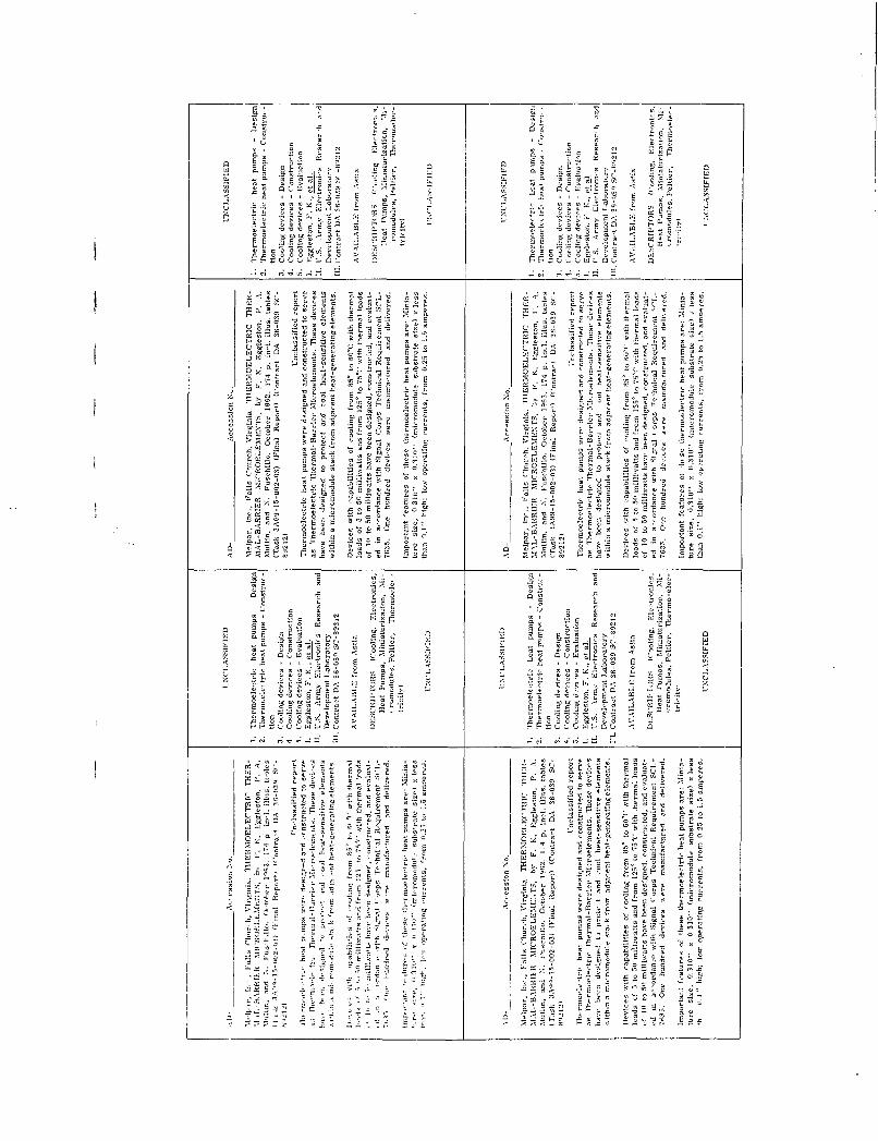
0* ,j*l 5 0. 0 -,-0 0 C.-CC
4, I 4,
.0 '� C,-I CO .0
10 (C t
01 (C 0 CC 0 Cito C 04 Ci-"o 4, - 244 a C(C �
C -2.5 � (C�X I C oC -'- .'1 04 �0o Z I Co 2.5 2.t��9Ci- -� (CoO tro'-7 4,0C. �i4 -
0.� 4,04, (C� ICi , CLOLC4,4,0 CO
.04, �-�'�ZIt�2. 0 042 CC-c .0 I I -C.00 ,
(CC, 04,0 2
-�, C. 24,04, 2.4Ci 4,4, � - �4, L.
cc 5-' vvo2cS.. 04(CC.
0'- 0 4 0 4 0 4 ... o.c -
55 W��"�s'� ES *5 .5 .5 � .S� � 04,
C. C. CCC� ----4,4,0000 CO
0 00 (CCC) C��/ CO
(C(C(CC(C4,O F.�0 0 0 0 0 0
�o
(4 �.4.A.W2C.2 �
CO �Ci 0
C.C.(Ct tAt�ao C.�
4(S0 4,(C . 4(C C. � C. (C '0
-Ci 0'0C.'- .0(C-.�.Li.o� 0 -4U�(C So 0(Ct � 4,4'
04Ci 04.4,004 Ci-oS 4-4, � "4,
U'ttCi 04, (C 04,
,jC'C--' o-' 04 'CC 0� '�CCCo(CO tt 0 :2� CC 000 0 C 04,CO at CCS2S5 0004! 0.� Ci -� '�t� 0004 C.
0 �i�o $.C.C. .�.g5 0 � /,C. 4,
-- co 5o'�00 .2� �4
� -, �,,4C'C2
0 4
Kc 54(.o(, 400'(C..& (C � �0IC *o
0' -� 0.0 0C.05 C.,5i- �� �i�.tP 2.s8t �4 Oij� to �- vt2 to(C Oa. 00" 4, i-i�2C-5 t�/ (0�(C - -z -- �'i-- * 0i-0 ��50i- �i- i- *�
05C.C. i,.0
*��00.0OS4,0
� 0 S$ .. '0 .0
4(0 - 0 .0 C.0400' � o5�.0 �C' 004, '.0
'04 *Ci 0i-(CO o'500
0 �.5'
04,i-
0 (C-000 0(CCC
4,04 �00 ,C 4'C0� t 4 t� � j4,(C , 0�Cw... i-C-� �Ci �f�a � �(C�O*.0 S�! C C �'0Ci
0' 0 0 0 -
0 04, 0
(Ci 0 (C Ci 0 0 Ci� �' - C-' '(C 4, -
tO (4 CiC 0( ot.5 C C 04 Ci4 �5 04,0 (CCnoCj 4, 0 004, 02 4 0 004,
-� 00�'ES�7 C. t2
'4rso� t4,04, 0� - 4(04, (Ct
* CLWVC.C.2. < 'C'" -0� S Li- Ci i ( C.
0 � 2 00
4,4,4, CO-Ci Z (C00Z4 ,
t� t410 � 4,4,0 4C
2Ci Ci 4'
C.C.C., - 045- CC C.C. 045- 20 zCtti--§Th< C,�
4(0�52O 04 2 5- 4,4,'. '-&C.C CCO(Ci- OO�04,Si. 04
C(C(t4�'0
C. Ci 0100'o(C(C0 00 .4 0404,4,
4(4,000004/4,44 000 no 4,440000444,0 00004.4,0
LUUCOCCCU UUC.COZCL
.- 040''.) ((CC) ' �' 'C��SC) C42... -0 (4(40
"4,4,"" (40" &t.sE� � EAt
- �&t� tnoE� 4, 0 4,0004, 'o-� 4, ,0�i-o.., iC
4-. C.
4 ,0(4 in 4,�4,04 cci-!S
0 k
5.o
�,t&4 , 0 0
.0'�t'o 0 .2 t"4 ( � �
02��'o 0i-(C 0 -
- oO C� . - oUCiC." 04, 0 (4 0CoootC -&�2.� cs -� -04, C'�o�
0004, 0> � (Ci-Ci 044004, �.0-4( (CC.
CO (4044, a0
C1 .4C42 *0
(CttO �O�04! a4C2
- 04 �4, � C.5.�( '-ut�t t*t�
C. '''� �04 I 0 04-'�C- 04,04, 4010�0 0
0' 0" C.4 ,
4 ,oi- � .0 5"-�2 to'-
� �'(0 �C.�0 � O� -04
5 >Cii-� 4t!.O 2.S�" OC. 0 E�to. 4,i-O' 0 4,0
4,.i. -� - i-� � 0" � .444.00 � �E �"- 2
04 "CCO 0 4 ,
i- 0�oo 04
-. 5 5a
0 O��'AO �Ci
- 0.00 -- .00400'(C'-.0Ci o 0
S--C. 4,* -i'ui-c 2' o2 05�� �
04�o 0-00 .0'.. '-o .0052.0 0
0?0S ((C (C *�4,
2. '-CC i-g � �
- �oo-- ,C-� 00 5 o