vlsi modeling and design - alexu.edu.eg
TRANSCRIPT
VLSI MODELING AND DESIGNDr. Mohammed M. Farag
FACULTY OF ENGINEERING - ALEXANDRIA UNIVERSITY
Instructor: Mohammed Morsy ([email protected]) 4th Floor ECE Building
TA: Eng. Mohamed Megahed
Office hours : Saturday 10:30 AM – 12:00 PM.
Course Webpage: http://eng.alexu.edu.eg/~mmorsy/Courses/Undergraduat
e/EE432_VLSI_Modeling_and_Design/EE432.html
Course Staff
EE 432 VLSI Modeling and Design 2
FACULTY OF ENGINEERING - ALEXANDRIA UNIVERSITY
Textbook “CMOS VLSI Design 4th ed.” Harris, David, and N.
Weste., (2010).
Reference books “Introduction to VLSI circuits and systems.” Uyemura,
John P. ,(2002). “Digital integrated circuits 2nd ed.” Rabaey, Jan M.,
Anantha P. Chandrakasan, and Borivoje Nikolic., (2002).
Course Text
EE 432 VLSI Modeling and Design 3
FACULTY OF ENGINEERING - ALEXANDRIA UNIVERSITY
VLSI Implementation Strategies. MOSFET non ideal characteristics. Delay models and logical effort. Power consumption and low-power design
considerations. Interconnect modeling, impact, and engineering. Robustness: Variability, Reliability, and Scaling. Design Methodologies and Tools. Testing, Debugging, and Verification.
Course Outline
EE 432 VLSI Modeling and Design 4
FACULTY OF ENGINEERING - ALEXANDRIA UNIVERSITY
4 Labs: 20 1 Project: 15 Midterm exam: 15 Final Exam: 75 Tools:
Electric http://www.staticfreesoft.com/ Tanner L-edit http://www.staticfreesoft.com/
Course Work
EE 432 VLSI Modeling and Design 5
FACULTY OF ENGINEERING - ALEXANDRIA UNIVERSITY
Lectures will make use of slides Slides are great ! Nice pictures to explain concepts Good addition for course text I can annotate them with a tablet PC I can switch to the tools and listings mid-lecture
Slides are horrible ! They make me teach 30% faster (really) They give you the sense that this is all easy stuff (it's not) They make you fall a sleep They make me lazy They make me waste time looking for clipart
Slides are a two-edged sword I encourage you to be active and take notes I may fall back to blackboard-based teaching occasionally
About the Lectures
EE 432 VLSI Modeling and Design 6
FACULTY OF ENGINEERING - ALEXANDRIA UNIVERSITY
History of VLSI
EE 432 VLSI Modeling and Design 7

FACULTY OF ENGINEERING - ALEXANDRIA UNIVERSITY
1959: Jack Kilby, working at TI, invented a monolithic“integrated circuit” Components connected by hand-soldered wires and
isolated by “shaping”, PN-diodes used as resistors (U.S.Patent 3,138,743)
The Integrated Circuit
EE 432 VLSI Modeling and Design 8
Figure 0.1 Diagram from patent application
FACULTY OF ENGINEERING - ALEXANDRIA UNIVERSITY
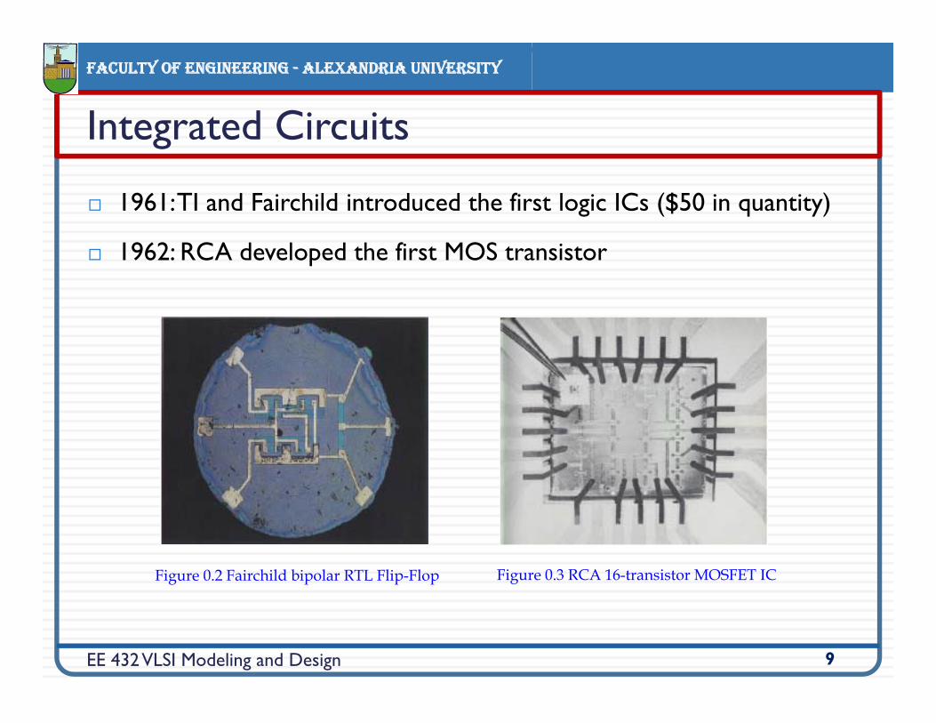
1961: TI and Fairchild introduced the first logic ICs ($50 in quantity)
1962: RCA developed the first MOS transistor
Integrated Circuits
EE 432 VLSI Modeling and Design 9
Figure 0.2 Fairchild bipolar RTL Flip-Flop Figure 0.3 RCA 16-transistor MOSFET IC
FACULTY OF ENGINEERING - ALEXANDRIA UNIVERSITY
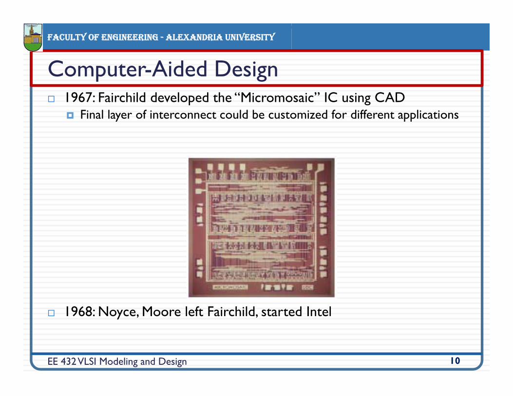
1967: Fairchild developed the “Micromosaic” IC using CAD Final layer of interconnect could be customized for different applications
1968: Noyce, Moore left Fairchild, started Intel
Computer-Aided Design
EE 432 VLSI Modeling and Design 10
FACULTY OF ENGINEERING - ALEXANDRIA UNIVERSITY
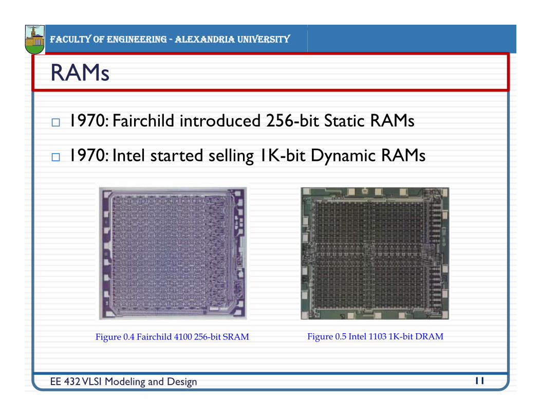
1970: Fairchild introduced 256-bit Static RAMs
1970: Intel started selling 1K-bit Dynamic RAMs
RAMs
EE 432 VLSI Modeling and Design 11
Figure 0.4 Fairchild 4100 256-bit SRAM Figure 0.5 Intel 1103 1K-bit DRAM
FACULTY OF ENGINEERING - ALEXANDRIA UNIVERSITY
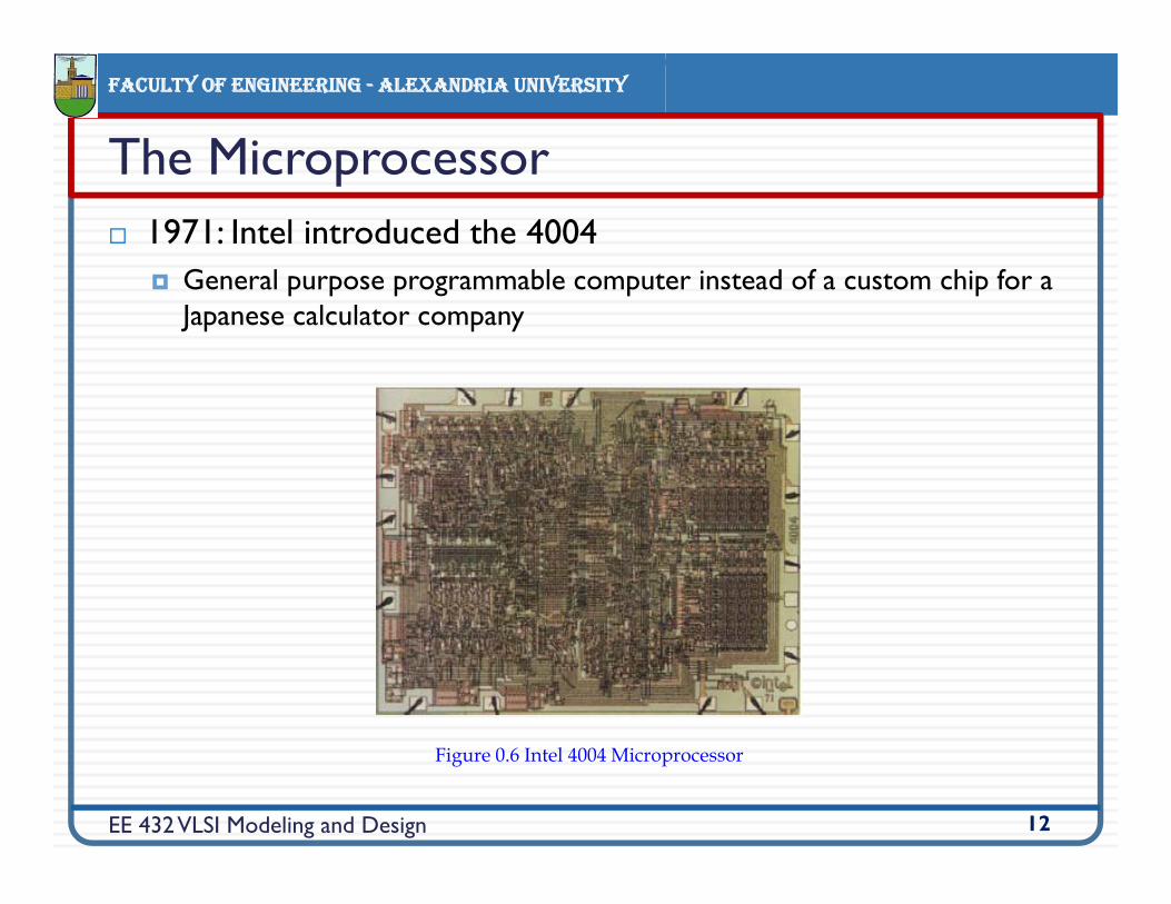
1971: Intel introduced the 4004 General purpose programmable computer instead of a custom chip for a
Japanese calculator company
The Microprocessor
EE 432 VLSI Modeling and Design 12
Figure 0.6 Intel 4004 Microprocessor
FACULTY OF ENGINEERING - ALEXANDRIA UNIVERSITY
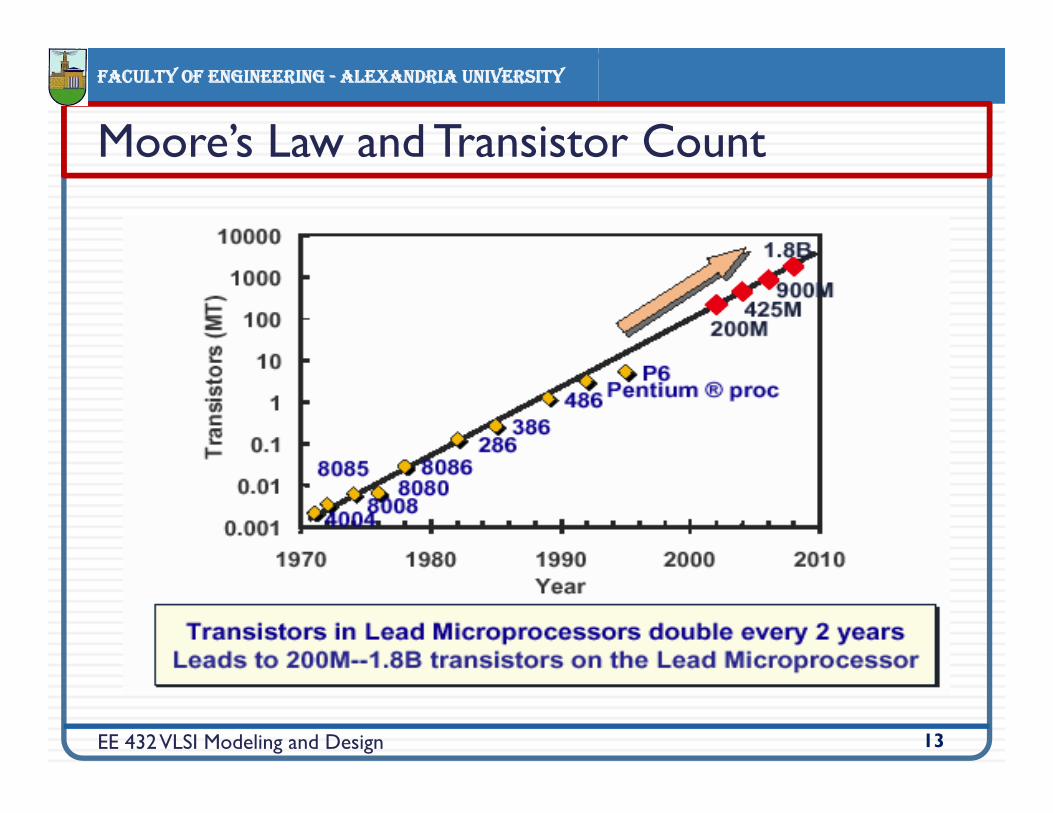
Moore’s Law and Transistor Count
EE 432 VLSI Modeling and Design 13
FACULTY OF ENGINEERING - ALEXANDRIA UNIVERSITY
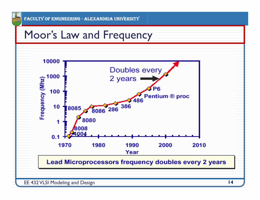
Moor’s Law and Frequency
EE 432 VLSI Modeling and Design 14
FACULTY OF ENGINEERING - ALEXANDRIA UNIVERSITY
Introduction
EE 432 VLSI Modeling and Design 15
FACULTY OF ENGINEERING - ALEXANDRIA UNIVERSITY
Introduction Complexity and Design Basic Concepts
Outline
EE 432 VLSI Modeling and Design 16
FACULTY OF ENGINEERING - ALEXANDRIA UNIVERSITY
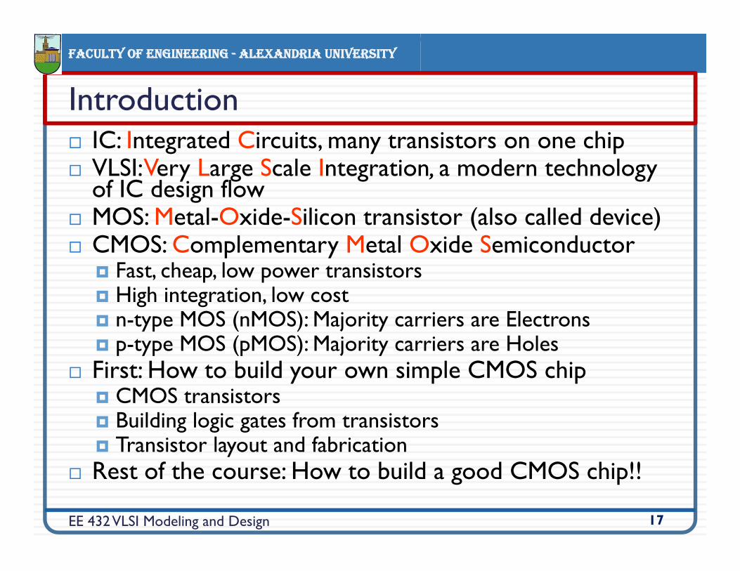
IC: Integrated Circuits, many transistors on one chip VLSI: Very Large Scale Integration, a modern technology
of IC design flow MOS: Metal-Oxide-Silicon transistor (also called device) CMOS: Complementary Metal Oxide Semiconductor
Fast, cheap, low power transistors High integration, low cost n-type MOS (nMOS): Majority carriers are Electrons p-type MOS (pMOS): Majority carriers are Holes
First: How to build your own simple CMOS chip CMOS transistors Building logic gates from transistors Transistor layout and fabrication
Rest of the course: How to build a good CMOS chip!!
Introduction
EE 432 VLSI Modeling and Design 17
FACULTY OF ENGINEERING - ALEXANDRIA UNIVERSITY
The term VLSI is used to collectively refer to many fields of electrical and computer engineering that deal with the analysis and design of very dense ICs
A VLSI chip contains more than 106 switching devices or logic gates
Early in the first decade of the 21st century, the actual number of transistors has exceeded 108 on a silicon die of typically 1 cm2 area
Introduction
EE 432 VLSI Modeling and Design 18
FACULTY OF ENGINEERING - ALEXANDRIA UNIVERSITY
Introduction Complexity and Design Basic Concepts
Outline
EE 432 VLSI Modeling and Design 19
FACULTY OF ENGINEERING - ALEXANDRIA UNIVERSITY
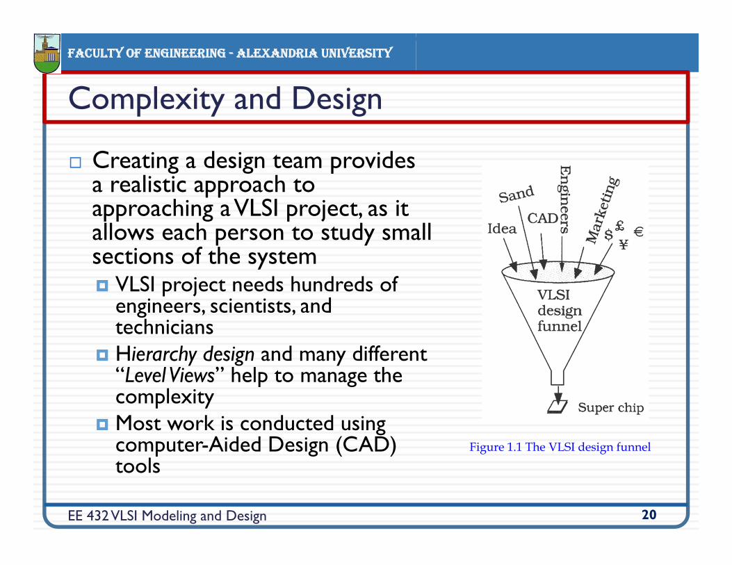
Creating a design team provides a realistic approach to approaching a VLSI project, as it allows each person to study small sections of the system VLSI project needs hundreds of
engineers, scientists, and technicians
Hierarchy design and many different “Level Views” help to manage the complexity
Most work is conducted using computer-Aided Design (CAD) tools
Complexity and Design
EE 432 VLSI Modeling and Design 20
Figure 1.1 The VLSI design funnel
FACULTY OF ENGINEERING - ALEXANDRIA UNIVERSITY
Design teams provide a realistic approach to develop a VLSI chip
The design hierarchy enables collaboration between team members and partitioning the work into a number of sub-tasks
The chip is viewed at many abstraction levels from the system specifications to the physical implementation.
Complexity and Design
EE 432 VLSI Modeling and Design 21
FACULTY OF ENGINEERING - ALEXANDRIA UNIVERSITY
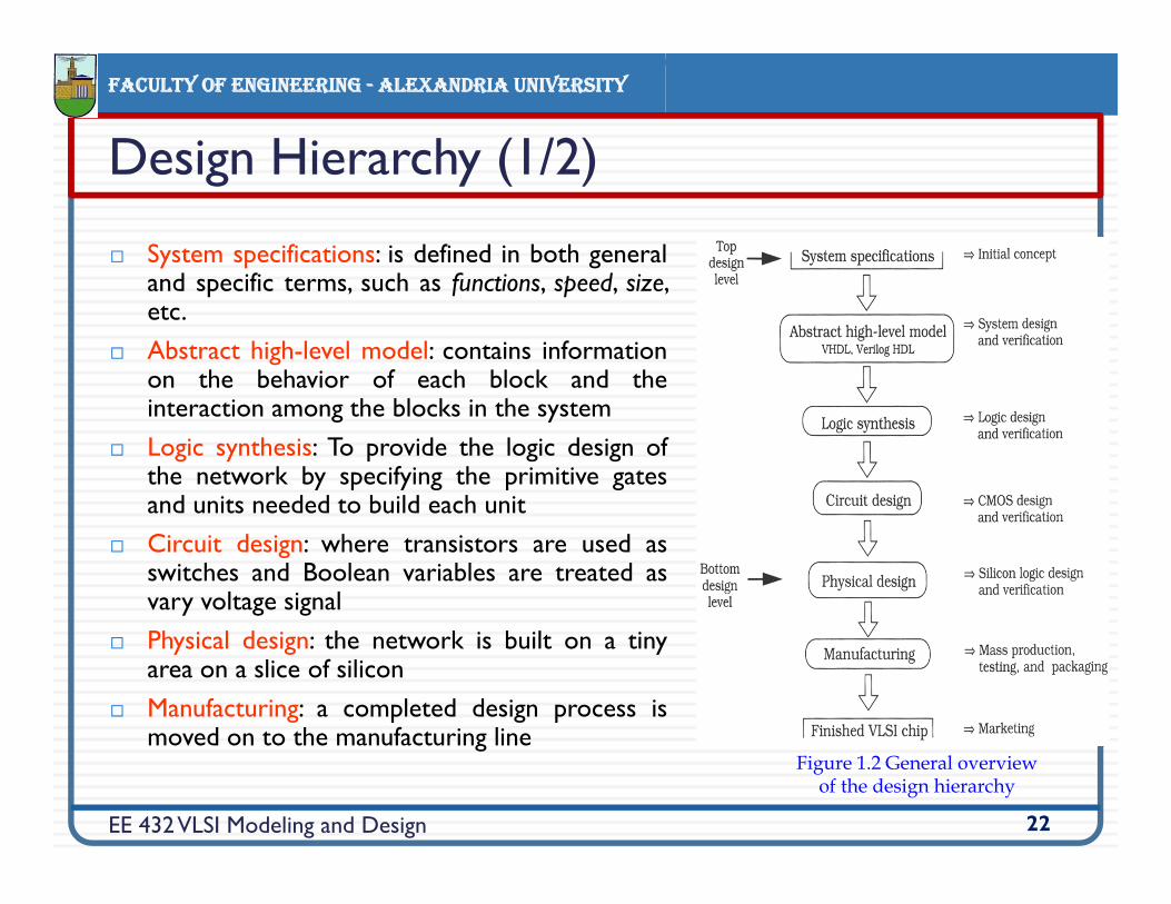
System specifications: is defined in both generaland specific terms, such as functions, speed, size,etc.
Abstract high-level model: contains informationon the behavior of each block and theinteraction among the blocks in the system
Logic synthesis: To provide the logic design ofthe network by specifying the primitive gatesand units needed to build each unit
Circuit design: where transistors are used asswitches and Boolean variables are treated asvary voltage signal
Physical design: the network is built on a tinyarea on a slice of silicon
Manufacturing: a completed design process ismoved on to the manufacturing line
Design Hierarchy (1/2)
EE 432 VLSI Modeling and Design 22
Figure 1.2 General overview of the design hierarchy
FACULTY OF ENGINEERING - ALEXANDRIA UNIVERSITY
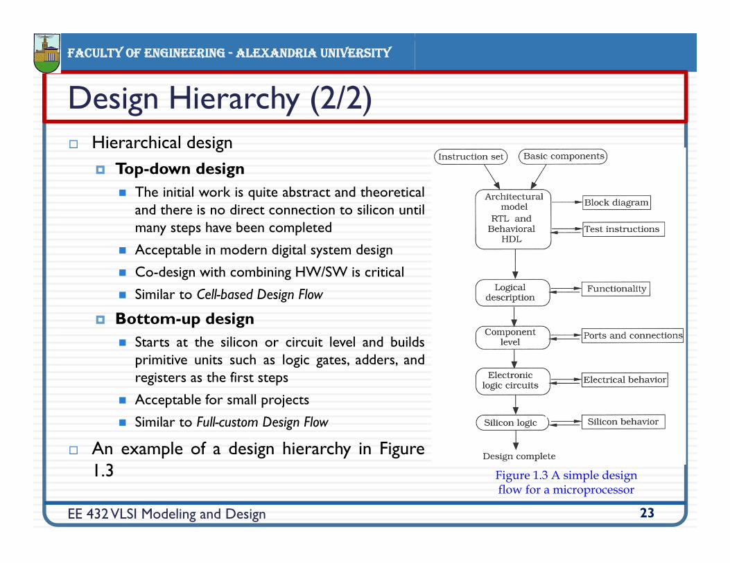
Hierarchical design Top-down design
The initial work is quite abstract and theoreticaland there is no direct connection to silicon untilmany steps have been completed
Acceptable in modern digital system design
Co-design with combining HW/SW is critical
Similar to Cell-based Design Flow
Bottom-up design Starts at the silicon or circuit level and builds
primitive units such as logic gates, adders, andregisters as the first steps
Acceptable for small projects
Similar to Full-custom Design Flow
An example of a design hierarchy in Figure1.3
Design Hierarchy (2/2)
EE 432 VLSI Modeling and Design 23
Figure 1.3 A simple design flow for a microprocessor
FACULTY OF ENGINEERING - ALEXANDRIA UNIVERSITY
At the engineering level, digital VLSI chips are classified by theapproach used to implement and build the circuit Full-custom Design: where every circuit is custom designed for the
project Extremely tedious Time-consuming process
Application-Specific Integrated Circuits (ASICs): using anextensive suite of CAD tools that portray the system design in terms ofstandard digital logic constructs Including state diagrams, functions tables, and logic diagram Designer does not need any knowledge of the underlying electronics or the
physic of the silicon chip Major drawback is that all characteristics are set by the architectural design
Semi-custom Design: between that of a full-custom and ASICs Using a group of primitive predefined cells as building blocks, called cell library
VLSI Chip Types
EE 432 VLSI Modeling and Design 24
FACULTY OF ENGINEERING - ALEXANDRIA UNIVERSITY
Introduction Complexity and Design Basic Concepts
Outline
EE 432 VLSI Modeling and Design 25
FACULTY OF ENGINEERING - ALEXANDRIA UNIVERSITY
VLSI Design is a system design discipline Many aspects can be taught without any reference to
the underlying silicon circuits System solutions can be generated using CAD tools Such an approach hides many details from the
designer However, many of the most powerful techniques and
ideas of VLSI reside at lower levels VLSI should be thought as a single discipline that
deals with the conception, design, and manufacture of complex ICs
Basic Concepts
EE 432 VLSI Modeling and Design 26
FACULTY OF ENGINEERING - ALEXANDRIA UNIVERSITY
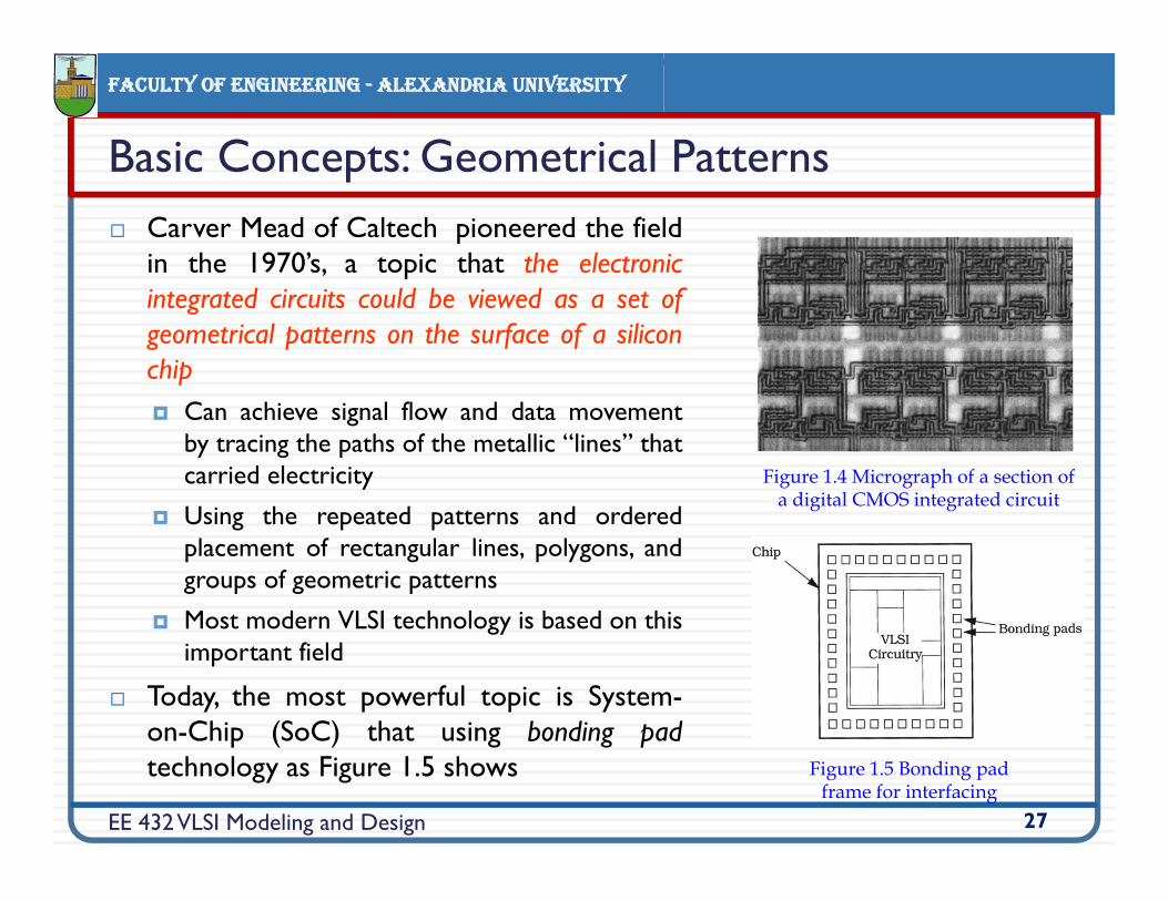
Carver Mead of Caltech pioneered the fieldin the 1970’s, a topic that the electronicintegrated circuits could be viewed as a set ofgeometrical patterns on the surface of a siliconchip Can achieve signal flow and data movement
by tracing the paths of the metallic “lines” thatcarried electricity
Using the repeated patterns and orderedplacement of rectangular lines, polygons, andgroups of geometric patterns
Most modern VLSI technology is based on thisimportant field
Today, the most powerful topic is System-on-Chip (SoC) that using bonding padtechnology as Figure 1.5 shows
Basic Concepts: Geometrical Patterns
EE 432 VLSI Modeling and Design 27
Figure 1.4 Micrograph of a section of a digital CMOS integrated circuit
Figure 1.5 Bonding pad frame for interfacing