volume 13, number 1 - meptec.org 13.1.pdf · from standard silver spot/ring to nick- ... volume 13,...
TRANSCRIPT
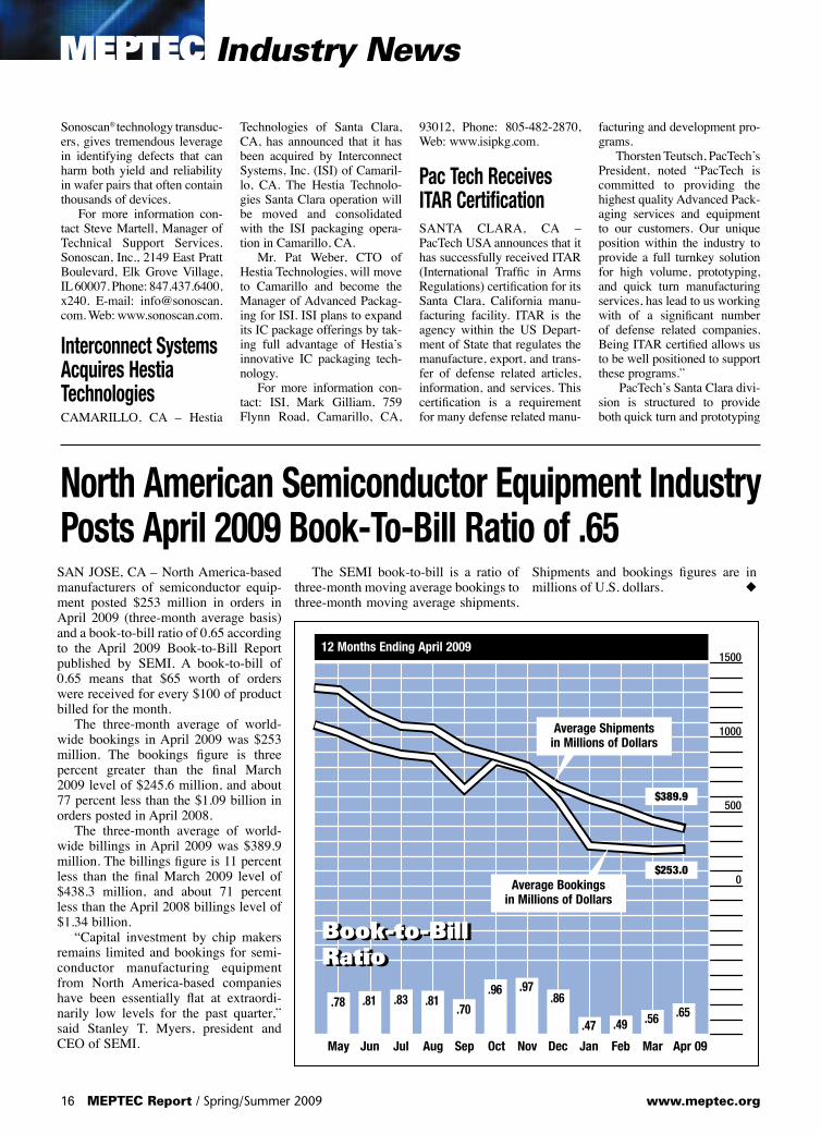
Book-to-Bill RatioFORAPRIL .65
MEMBER COMPANY PROFILE
ASM Pacific Technology’s mission state-ment is “To be the leading integrated sys-tem and materials supplier to the global microelectronics industry, offering complete factory automation solutions to customers for their assembly and packaging needs and providing total customer satisfaction with our innovative, cost-effective products.” In following that mission statement over the last 30+ years, ASM Pacific Technology Ltd. is today the largest supplier of IC assembly equipment to the world and has been since 2002. page 10
Semiconductor equipment bookings decrease 3% over March 2009 level. page 16
A SM has become one of the top leadframe suppliers in the world with capability in both stamped and etched
frames and with plating capability from standard silver spot/ring to nick-el-palladium-gold for lead free process-ing and the more advanced Brown Oxide for improved moisture sensitiv-ity protection needs of today’s most challenging packages. Recently, ASM released their new high density QFN type package for very high I/O counts.
A Publication of The MicroElectronics Packaging & Test Engineering Council
www.meptec.org Spring/Summer 2009 / MEPTEC Report 1
INDUSTRY NEWS
Honeywell has developed a new thermal inter-face material to help manage heat produced by advanced semiconductors. page 14
Rudolph Technologies, Inc. has announced the sale of its Explorer® Inspection Cluster to a major memory manufacturer in Taiwan. page 14
Sonoscan will introduce its new C-SAM®
series AW300™ for bonded wafer inspection at Semicon West. page 15
PacTech USA has successfully received ITAR (International Traffic in Arms Regulations) certification for its Santa Clara, California manufacturing facility. page 16
March Plasma Systems has announced that it has qualified its advanced PROVIA™ plasma system at a leading European PCB manufac-turer. page 17
Volume 13, Number 1
SPRING/SUMMER 2009
SEMICON West returns to Moscone Center in San Francisco July 14 through 16. page 27
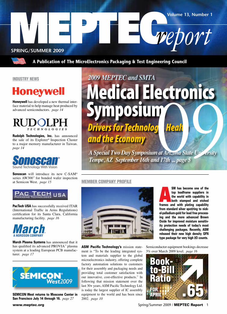
A Special Two Day Symposium at Arizona State University Tempe, AZ September 16th and 17th ... page 5
Medical Electronics SymposiumDrivers for Technology, Healthand the Economy
2009 MEPTEC and SMTA
09

I t’s that time again: summertime, which in our industry means Semicon West. Despite the economy, SEMI has pulled together some great programs, and their current list of exhib-itors is strong. Even in tough times it is still
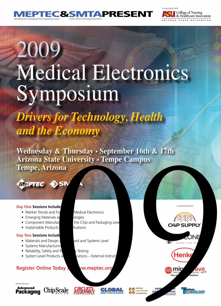
important for people to come together to learn and show their products and services. Trade associations such as SEMI and MEPTEC and many others are an important component in a company’s promotional activities. MEPTEC’s next event is 2009 Medical Elec-tronics Symposium: Drivers for Technology, Health and the Economy, and for the fourth year is being held at the Old Main building at Arizona State Uni-versity. We’re pleased to announce that this year we will be holding this event jointly with SMTA, and expanding it from one day to two. To prepare this two day agenda which will cover a broad spectrum of medical applications, Day One will focus primar-ily on the “chip level” component packaging and testing and Day Two will focus on board assembly and systems levels. Sponsorships are also available. See page 5 for further information. Our Industry Analysis this issue is from Richard Wawrzyniak of Semico Research Corporation on “SoC Design Costs: Perspectives on an Important Issue” (see page 6). Richard discusses how out-sourcing drives new markets and the escalating cost of complex SoC design. He believes that properly understanding the costs and the forces that drive them can help companies navigate through poor economic conditions and emerge stronger. We’re covering Purdue University this issue as our University Profile. Purdue covers a great deal of technology relevant to our industry in their curricu-lum, namely microelectronics, energy and biomedi-cal engineering. In microelectronics they are helping to solve the lead-free solder problem by working on solutions to prevent tin whiskers, and creating nano-solders to help reduce costs in manufacturing. Under energy technology, they are working on the development of nanomaterials and new devices for energy conversion. In the biomedical arena, one
professor’s research focuses on wound healing by developing materials which when injected into the body will help repair damaged bones, spinal cords, etc. See page 8 for this venerable institution’s story. Our Company Profile this issue is from long-time MEPTEC corporate member, ASM Pacific. ASM has a large offering of equipment and services and has served the industry for over 30 years. Their main mission is putting the customer first, and they do it well with their many products and services and their worldwide team of experts. See their story on page 10. Our first Feature Article is from long-time MEPTEC member, ASE (U.S.), Inc. Bernd Appelt, Director of World Wide Business Development wrote “The Road to 4th Generation fsCSP Packag-ing Substrates”. He explains how by taking a “holis-tic” approach to fcCSP can result in a low cost, high volume product can be developed (see page 18). Thanks to Bernd for this informative article. Our next Feature Article is from a speaker at two recent very well attended MEPTEC luncheons in Sunnyvale and Phoenix, Sanjiv Taneja of Cadence Design Systems. Sanjiv writes about the “Role of Manufacturing Test & Packaging in Optimizing the Design Chain” (see page 13). He discusses the challenges and opportunities between the EDA and IC packaging industries. We’d like to thank Sanjiv for bringing this perspective to our members and supporters. Our Editorial this issue is from MEPTEC Advi-sory Board member, Nick Leonardi. Nick discusses “Business...the Fair Exchange of Values”. He talks about the “fair exchange of values” in terms of business relationships and current business environ-ments. Thanks to Nick for this thoughtful disserta-tion. We’d like to thank all of our contributors for making this another great issue. If you’re reading this publication for the first time at the Semicon West show, or another of the many events where we distribute we hope you enjoy it. Thanks for read-ing! ◆
Council UpdateVolume 13, Number 1
A Publication of The MicroElectronics Packaging
& Test Engineering Council
P. O. Box 222Medicine Park, OK 73557
Tel: (650) 714-1570 Email: [email protected]
Published ByMEPCOM
EditorBette Cooper
Design and ProductionGary Brown
Sales ManagerGina Edwards
––––––––––––––
MEPTEC Advisory Board
Seth AlaviSunSil
Jeffrey BradenAtmel Sensor Group
Philippe BriotP. Briot & Associates
Joel CamardaGTronix
Gary CatlinPlexus
Tom Clifford
Rob Cole
John CraneJ. H. Crane & Associates
Jeffrey C. DemminTessera
Bruce EuzentAltera Corporation
Skip Fehr
Julia GoldsteinAdvanced Packaging Magazine
Anna GualtieriElle Technology
Bance HomConsultech International, Inc.
Ron JonesN-Able Group International
Nick LeonardiPremier Semiconductor Services
Phil MarcouxTPL Group
Mary OlssonGary Smith EDA
Marc PapageorgeSemiconductor Outsourcing Solutions
Mike PinelisMEMS Investor Journal
Rich RiceASE (US) Inc.
Dr. Michael ToddHenkel Corporation
Jim WalkerGartner Dataquest
Russ WinslowSix Sigma
––––––––––––––
MEPTEC Report Vol. 13, No. 1. Published quarterly by MEPCOM, P. O. Box 222, Medicine Park, OK 73557. Copyright 2009 by MEPTEC/MEPCOM. All rights reserved. Materials may not be reproduced in whole or in part without written permission.
MEPTEC Report is sent without charge to members of MEPTEC. For non-members, yearly subscriptions are avail-able for $75 in the United States, $80US in Canada and Mexico, and $95US elsewhere.
For advertising rates and information contact Gina Edwards at 408-858-5493, Fax Toll Free 1-866-424-0130.
www.meptec.org Spring/Summer 2009 / MEPTEC Report 3
MEPTEC Welcomes New Advisory Board MemberDr. Michael Todd will replace Bhavesh Muni as Henkel’s representative on MEPTEC’s Advisory Board. We would like to acknowledge Bhavesh’s valuable contributions to MEPTEC over the past couple of years. As a member of the Henkel Leadership Team and the Vice-President of Product Development and Engineering, Dr. Michael Todd has visibility of all materials innovation initiatives at Henkel. His materials science expertise and knowledge of forward-looking technology requirements will positively contribute to the advancement of MEPTEC. Dr. Todd is Vice-President of Product Development and Engineering for Henkel Corporation’s electronics group, where he leads a global team developing next-generation materials for electronics assembly and microelectronic packaging. Todd received his Ph.D. in materials science engineering from the University of California, Irvine, his Masters degree in Materials Science Engineering from the University of Michigan and bachelors degrees in Chemistry and Materials Science Engineering from the University of California, Los Angeles. ◆
Radisson Hotel. San Jose, CA www.memstestreliability2009.com
Co-Produced by MEMS Investor Journal and MEPTEC
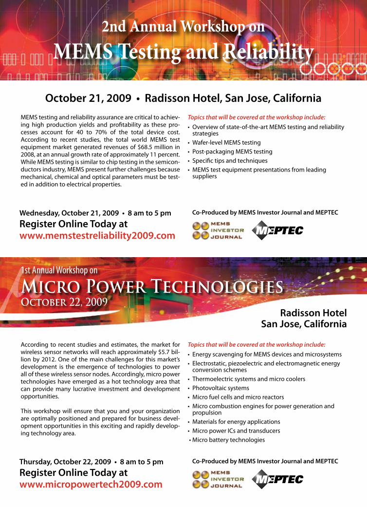
2nd Annual Workshop onMEMS Testing and Reliability
Wednesday, October 21, 2009 • 8 am to 5 pmRegister Online Today at www.memstestreliability2009.com
MEMS testing and reliability assurance are critical to achiev-ing high production yields and profitability as these pro-cesses account for 40 to 70% of the total device cost. According to recent studies, the total world MEMS test equipment market generated revenues of $68.5 million in 2008, at an annual growth rate of approximately 11 percent. While MEMS testing is similar to chip testing in the semicon-ductors industry, MEMS present further challenges because mechanical, chemical and optical parameters must be test-ed in addition to electrical properties.
Topics that will be covered at the workshop include: • Overview of state-of-the-art MEMS testing and reliability strategies• Wafer-level MEMS testing• Post-packaging MEMS testing• Specific tips and techniques• MEMS test equipment presentations from leading suppliers
Co-Produced by MEMS Investor Journal and MEPTECThursday, October 22, 2009 • 8 am to 5 pmRegister Online Today at www.micropowertech2009.com
According to recent studies and estimates, the market for wireless sensor networks will reach approximately $5.7 bil-lion by 2012. One of the main challenges for this market’s development is the emergence of technologies to power all of these wireless sensor nodes. Accordingly, micro power technologies have emerged as a hot technology area that can provide many lucrative investment and development opportunities. This workshop will ensure that you and your organization are optimally positioned and prepared for business devel-opment opportunities in this exciting and rapidly develop-ing technology area.
Topics that will be covered at the workshop include:• Energy scavenging for MEMS devices and microsystems• Electrostatic, piezoelectric and electromagnetic energy conversion schemes• Thermoelectric systems and micro coolers• Photovoltaic systems• Micro fuel cells and micro reactors• Micro combustion engines for power generation and propulsion• Materials for energy applications• Micro power ICs and transducers • Micro battery technologies
1st Annual Workshop on
Micro Power TechnologiesOctober 22, 2009
Radisson HotelSan Jose, California
October 21, 2009 • Radisson Hotel, San Jose, California
Media Sponsors
2009Medical ElectronicsSymposiumDrivers for Technology, Healthand the Economy
MEPTEC&SMTAPRESENTMicroelectronics Packaging & Test Engineering Council Surface Mount Technology Association
In Association With
Wednesday & Thursday • September 16th & 17thArizona State University • Tempe Campus Tempe, Arizona
Day One Sessions Include: • Market Trends and Forecast in Medical Electronics • Emerging Materials and Technologies • Component Manufacturing at the Chip and Packaging Level • Implantable Products and Applications
Day Two Sessions Include: • Materials and Design at the Board and Systems Level • Systems Manufacturing • Reliability, Safety and Regulatory Testing • System Level Products and Applications – External Instrumentation
Register Online Today at www.meptec.org
Corporate Sponsors
2nd Annual Workshop onMEMS Testing and Reliability
09

MEPTEC Industry Analysis
6 MEPTEC Report / Spring/Summer 2009 www.meptec.org
A pproximately thirteen years ago, ASIC vendors were busy assimi-lating 0.5mm process capabili-ties and creating large libraries of functional blocks (which later
became better known as SIP) to be utilized in their Standard Cell product lines. While continual advances in semiconductor manu-facturing processes were well documented and even expected, the design side of the product creation equation was lagging farther and farther behind process capabilities. The creation of these large Standard Cell libraries offered designers a shortcut towards the goal of placing new designs into the market more quickly as opposed to pursuing a full custom implementation. But in reality, the respite was only temporary since the existence of these libraries did little to permanently reduce the gap between the ability to craft a new design and the ability to produce it. Starting the mid-1990s, customers asked their ASIC silicon suppliers for more access to and control over the design process. This was done because it was thought that greater involvement in the design would allow for greater differentiation in the silicon solution, and to a large degree this was true. Thus was born the System-on-a-Chip (SoC) industry. This trend also gave rise to the 3rd Party Semiconductor Intellectual Property (SIP) market. Now customers could incorporate SIP into their designs, essentially capturing bits of expertise frozen in time from many different vendors, capitalizing on the investment made by these 3rd Party SIP vendors and preserve more of their own internal design resources while at the same time achieving greater dif-ferentiation in their own silicon solutions. In reality, this was a continuation of trends that started in the early 1970s with the disaggrega-tion of the semiconductor market. Figure 1 gives a representation of just how the trend towards disaggregation has progressed over the last 30 years and how it should play out over the rest of this decade. Disaggregation has played a critical role in helping to create industries for process equip-ment, ASIC design services, mask making ser-vices, foundry services, fabless semiconductor companies and finally, semiconductor IP. One of the prime movers behind this disaggregation has been Moore’s Law. The constant increase in the potential number
of gates that can be produced on a die each time the industry reaches the next process node has allowed designers to add many functions virtually for ‘free.’ In addition, the continual reduction in device cost possible due to Moore’s Law has enabled and fueled many new markets and applications that have been able to absorb all the additional performance and new capability of each new process gen-eration. However, this greater customer interaction and design flexibility came with a price. This change in the design methodology shifted more of the responsibility of getting the design right from the vendor to the customer. Now the customer must understand his applica-tion in very great detail to ensure that all the
nuances of the application are captured in the silicon. A further complication in the life of the SoC designer today is the continual rise in the transistor budget available at each suc-ceeding process node. This has caused the level of complexity possible to SoCs to rise dramatically and has caused the design cycle times to lengthen and design costs to escalate precipitously over the last 5 to 8 years. The subject of design costs for complex SoC sili-con solutions evokes much heated debate in semiconductor industry circles today. Semico believes it is important to note when in the life of a particular process geom-etry a chip is designed. It is fair to say that the design costs for a chip at the very beginning
SoC Design Costs: Perspectives on an Important Issue Richard WawrzyniakSr. Market Analyst, ASIC & SoCSemico Research Corp.
Figure 1. Outsourcing Drives New Markets Source: Semico Research Corp.
Figure 2. Escalating Cost of Complex SoC Design Source: Semico Research Corp.

of the 65nm or 45nm process node will not be the same as if that exact part were designed in the middle of the life cycle or even at the end of the life cycle for that geometry. One of the underlying principles of the semicon-ductor industry is the data and experience gathered from the so-called ‘learning curve’ can be applied to future production to improve yields and reduce costs. The same is true for the design effort. As more designs are done at a given process node, the effort becomes more efficient and somewhat easier from each design on to the next. This is attributable to designers becoming more familiar and com-fortable with all the aspects in the design effort – from the use of the EDA tools to a better understanding of the manufacturing process itself to the point where they can anticipate potential pitfalls in a design and avoid them. Semico believes that costs at the 45nm node for complex SoCs can reach $60M+ if all the design parameters for the silicon are maxed out – largest possible die area, highest transistor budget possible at the geometry in question, fastest clock speed, largest number of I/Os, etc. As figure 2 shows, the cost of complex SoC designs has risen for every process geom-etry since the 250nm node. We believe this is likely to continue into the foreseeable future. However, this does not mean that every SoC design must incur the costs shown above. It is entirely possible to craft complex silicon solutions for less than these amounts if the right amount of 3rd Party SIP is used in con-junction with an accurate understanding of the end application and a judicious incorporation of feature sets and functionality that address market requirements.
Why is this so important? Simply because if rising design costs become so high as to prevent companies from undertaking their next ASIC or SoC design, then the industry, as we know it today, will suffer dramatic and drastic changes. Undeniably, the semiconductor in-dustry, and the larger electronics industry, depends on a continual flow of up-to-date products to bring innovation to the market and to capture and meet changing market require-ments. If this flow of new products and inno-vations slows or stops, it is possible we will see an overall reduction in market demand as consumers will not highly value warmed-over versions of already existing products. Accurately understanding the design costs for ASIC and complex SoC designs is necessary for correctly evaluating whether or not such a design should be undertaken or if it can provide the return on the initial investment in people, resources and time needed to make it worthwhile for the design-ing company. Semico believes that properly understanding these costs, and the underlying forces that drive them, can help companies correctly navigate through our current poor economic conditions and emerge a stronger competitor in the future. ◆

P urdue University’s College of Engineering is responding to the global challenges of the 21st century with research that focus-es on projects that will expand
the boundaries of science and technology and impact the well being and prosperity of humanity with compassion and concern for the sustainability of the Planet. Purdue, located in West Lafayette, Indi-ana, is a Land Grant university with a global perspective. Its internationally recognized College of Engineering is a prime source of fulfilling both the Land Grant mission and the worldwide view.
Microelectronics Carol Handwerker, a Professor of Mate-rials Engineering, is among the researchers involved in an international effort to perfect environmentally friendly solders that don’t contain lead, which has been banned in Europe and China. “This is a global issue because, sooner or later, we’re all going to convert to lead-free solder,” says Handwerker, who has specialized in electronic interconnects for nearly 15 years. One obstacle to developing lead-free solders is finding ways of preventing the spontaneous formation of tin whiskers that cause electrical shorts. In a conventional solder made of tin and lead, the lead pre-vents the formation of extremely small particles, says Handwerker, who previously worked at the National Institute of Stan-dards and Technology, where she led efforts to help industry convert to lead-free solder. Another key problem that must be solved is that lead-free solders have higher melting points than lead-tin solder, making it more expensive to manufacture prod-ucts using alternative solders. A potential solution is to create nano-solders out of extremely small particles that melt at lower temperatures than the bulk counterparts. Researchers are trying to shrink the par-ticles from their current size of about 100 microns, or millionths of a meter, to 10 nanometers, or billionths of a meter, thus reducing the melting temperature by 40 degrees Centigrade. To help solve the lead-free solder prob-lems, Purdue joined the International Elec-
tronics Manufacturing Initiative, an industry-led consortium whose mission is to assure leadership of the global electronics manu-facturing supply chain. Purdue is one of two university members out of a total member-ship of about 70 electronics manufactur-ers, suppliers, associations and government agencies.
Energy Researchers around the College are tack-ling the energy challenge. Among them is Hugh Hillhouse, an Associate Professor of Chemical Engineering. Hillhouse and his research group are working on the develop-ment of nanomaterials and new devices for energy conversion. Hillhouse has developed membranes with small pores – less than five nanometers
in diameter – to template the formation of small diameter semiconductor wires. He and his team are the first to develop a method to make the films so that they self assemble, which means they form automatically under the proper laboratory conditions without costly manufacturing processes. The technique could dramatically lower the cost of electricity from solar cells and is suitable for mass manufacturing at reasonable prices. This could lead to solar cells that are economically competitive with other forms of power generation, such as coal-fired power plants. “The energy problem has been prescient on my mind for a very long time,” Hill-house says. “Fossil fuel resources will run out, and issues with CO2 emissions and the burning of fossil fuels make it imperative that we develop clean energy and find ways to make it happen.” Purdue engineers are also working on such technologies as more efficient heat pumps for space heating in buildings and domestic water heating, compressors that integrate devices to recover energy ordinar-ily lost, systems that use naturally occurring “green working fluids” such as air or carbon dioxide as a refrigerant, and designs that modify the conventional vapor compression cycle behind refrigeration. “Compressors, air conditioners and refrigerators are responsible for a huge portion of the world’s total energy con-sumption,” says Eckhard Groll, a Purdue
Purdue Engineering researchers tackle global problems across a broad range of topics, focusing on creating a better world
MEPTEC University News
8 MEPTEC Report / Spring/Summer 2009 www.meptec.org
Carol Handwerker (left), Professor of Materials Engineering and Hugh Hillhouse, Associate Professor of Chemical Engineering at Purdue.

Professor of Mechanical Engineering and head of the college’s Office of Professional Practice. “As energy prices increase, so too does interest in more efficient systems.” Carbon dioxide makes an environmen-tally friendly refrigerant because it has a much lower global warming potential than synthetic refrigerants now on the market, says Groll, who works on design optimiza-tion and reliability studies for air condi-tioning, heating, cooling, and ventilation systems. The Thermal Systems Research Group, which includes Groll, is studying a system using the Ericsson cycle, which is an alter-native to the traditionally dominant air con-ditioning and refrigeration technology of vapor compression, and uses an alternative cycle technology that can provide cooling capacity. The Ericsson cycle is based on an exotic concept called isothermal compression and expansion to induce cooling. Unlike con-ventional refrigerators, in which a refrig-erant gas condenses into a liquid after absorbing heat, the refrigerant remains a gas in the Ericsson cycle. The gas is kept cool by adding a liquid to it as it is being compressed, and the system could replace synthetic refrigerants with natural materi-als such as air, nitrogen or carbon dioxide. Because the system is flexible with respect to the gas and liquid used, it can be charged with many different gases for environmen-tally friendly operation. Health Across campus at the Weldon School of Biomedical Engineering, Purdue engineers are exploring ways to improve the quality of human life directly. Alyssa Panitch, an Associate Professor of Biomedical Engi-neering, specializes in bio-organic chemis-
try, with particular interest in the design and synthesis of biomaterials for drug delivery and tissue engineering. Among her projects is one that focuses on wound healing. She is developing scaffold-like materials designed to be injected into the body where they will quickly solidify to fit any space, repairing damaged bones, spinal cords, arteries and other tissues. Because the material starts out as a liq-uid, it fills in the gaps between damaged or missing tissue before hardening into a gel, or three-dimensional matrix that eventually disintegrates as it is replaced by healthy tis-sue, Panitch says. This gel could be loaded with time-released therapeutic drugs, such as growth factors needed to enhance healing. The approach also could be used to improve drug-eluting stents, which are metal scaf-folds inserted into arteries to keep them open after surgeries to treat clogs. Once in place, the stents release therapeutic agents, but scientists have recently learned that the stents can cause new clogs, leading to heart attacks. The method harnesses natural interac-tions in the body between molecules called polysaccharides and protein building blocks called peptides to control the assembly of the three-dimensional matrices. The poly-saccharides interact with proteins and help the proteins come together and assemble scaffolds. Researchers have used the interaction between a polysaccharide called heparin and a peptide fragment of a protein called antithrombin III, which is contained in the bloodstream to control clotting. The proteins exist in the extracellular matrix located between cells in tissues, where cells secrete the protein molecules. Researchers attached heparin-binding pep-tides from antithrombin III to a synthetic material called polyethylene glycol. Mix-ing solutions of this peptide-polyethylene glycol combination with heparin instantly produces a three-dimensional matrix. “It’s very rapid assembly,” says Panitch. Other Purdue researchers have created a precise biosensor for detecting blood glu-cose and potentially many other biological molecules by using hollow structures called single-wall carbon nanotubes anchored to gold-coated nanocubes. The device resem-bles a tiny cube-shaped tetherball. Each tetherball is a sensor and is anchored to electronic circuitry by a nanotube, which acts as both a tether and ultrathin wire to conduct electrical signals, says Timothy Fisher, a Purdue Professor of Mechanical Engineering. The technology, which detects glucose more precisely than any biosensors in development, also might be used in medi-cine to detect other types of biological mol-ecules and in future biosensors for scientific
research, according to Marshall Porterfield, an Associate Professor of Agricultural and Biological Engineering at Purdue. The single-wall nanotubes are espe-cially suited for electronic sensors because electricity flows more efficiently through wires only a few nanometers in diameter than it does through ordinary wires. “It might be part of a catheter to contin-uously monitor blood glucose for diabetics. And it might have many other applications, including basic scientific research to study diseases and biological processes,” Por-terfield says. “If we can allow someone to monitor their disease and have a better qual-ity of life, that’s great. But what if we could develop a tool that would allow scientists to discover the cure for that disease?” Developing technology and materials to benefit human health, contribute to environ-mental sustainability, and deliver alterna-tive energies – these are just a few of the challenges that motivate Purdue researchers who are on a mission to make a difference in the world. ◆
www.meptec.org Spring/Summer 2009 / MEPTEC Report 9
Purdue University College of Engineering Facts
Fall 2008 Enrollment: 6,735 undergraduate students 2,331 graduate students
Faculty: 348
Schools: Aeronautics and Astronautics, Agricultural and Biological Engineering, Biomedical Engineering, Chemical Engineering, Civil Engineering, Construction Engineering and Management, Electrical and Computer Engineering, Engineering Education, Engineering Professional Education, Environmental and Ecological Engineering, Industrial Engineering, Materials Engineer-ing, Mechanical Engineering, Nuclear Engineering.
Programs: Engineering Projects in Community Service (EPICS), First-Year Engineering Program, First-Year Engineering Honors Program, Global Engineering Program, Minority Engineering Program, Professional Practice Program, Women in Engineering Program.
Alumni: More than 70,000, including the first and most recent astronauts to walk on the moon.
Milestones: First Department of Freshman Engineering (1953), first Women in Engineering Program (1969), founding site of the National Society of Black Engineers (1971-1975), founding site of EPICS (1995), first department dedicated to engineering education (2004)
Purdue researchers have created a precise biosensor for detect-ing blood glucose by using hollow structures called single-wall carbon nanotubes anchored to gold-coated nanocubes.
Purdue Mechanical Engineering Professor Eckhard Groll works on design optimization and reliability studies for HVAC systems.
To be or not to be… one of the most well known and used opening lines ever written.
A t ASM Pacific Technology, their mission statement is: “To be the leading integrated system and materials supplier to the global microelectronics industry, offer-
ing complete factory automation solutions to customers for their assembly and packaging needs and providing total customer satis-faction with our innovative, cost-effective products.” In following that mission statement over the last 30+ years, ASM Pacific Technol-ogy Ltd. is today the largest supplier of IC assembly equipment to the world and has been since 2002. ASM also provides the widest range of products with equipment for all major process steps of die attach, wire bond, encapsulation and post-encapsulation. ASM has equipment offerings to serve every major market of device assembly including the IC, LED, COB and Discrete markets. ASM has also become one of the top leadframe suppliers in the world with capa-bility in both stamped and etched frames and with plating capability from the stan-dard silver spot/ring to the nickel-palladium-gold for lead free processing and the more advanced Brown Oxide for improved mois-ture sensitivity protection needs of today’s most challenging packages. Most recently, ASM released their new high density QFN type package for very high I/O counts called DreamPAK™. This wide product, process and market portfolio allows ASM to help customers bring their products to market faster and with
more assurance of success than at any other time in the history of the industry. Founded in Hong Kong in 1975 as the Asian marketing arm for ASM International, ASM grew rapidly. By 1980, ASM Assem-bly Automation was established with its product line of semi-automatic wire bonders and 3rd optical inspection stations. In 1980, ASM also opened it leadframe stamping and plating operation to supply materials to the IC market. By 1984, ASM had launched a new line of fully automatic gold wire ball bonders with the AB300 series. Their success in this market allowed for contin-ued growth and successful penetration to a number of local IC subcontractor companies in the Asian region. ASM was already the dominant player in the LED and COB mar-ket at this time. In 1989, ASM Pacific Technology Ltd was formally listed on the Hong Kong Exchange as a public company. ASM Inter-national continues as its majority sharehold
er with an ~53% stake (a good investment considering ASM Pacific’s rate of return to investors and 33 years of positive operat-ing results). Also in this same year, ASM opened its state-of-the-art fabrication and sub-assembly factory in the Shenzhen area of China. In 1990, ASM expanded operations to Singapore with the initial establishment of our second R&D center, etched leadframe operation and manufacturing facility for the gold wire ball bonding products. Continued growth through the 1990s allowed ASM to expand operations with increased capacity in China and the addition of a factory in Johor Malaysia to support customer needs. The continued performance improvements in all aspects of their product portfolio have also helped ASM penetrate into the entire world of IC packaging includ-ing the most demanding customers. Their customer base now extends into every major and regional subcontractor as well as the largest IDM companies world wide. Their
MEPTEC Member Company Profile
10 MEPTEC Report / Spring/Summer 2009 www.meptec.org
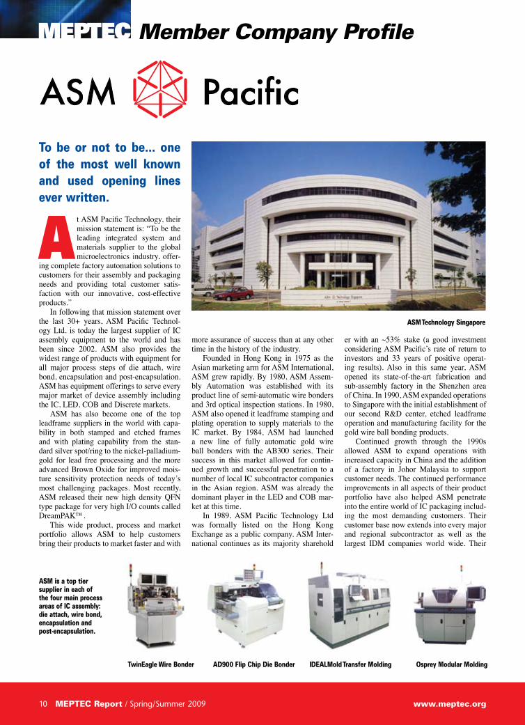
ASM Technology Singapore
ASM is a top tier supplier in each of the four main process areas of IC assembly: die attach, wire bond, encapsulation and post-encapsulation.
TwinEagle Wire Bonder AD900 Flip Chip Die Bonder IDEALMold Transfer Molding Osprey Modular Molding

FSE support and marketing teams are also located in every major Assembly and Pack-aging region across the globe so as to sup-port their customer base. Since the turn of the new century, ASM has worked to position itself not just as the overall market leader but also as a leader in each market segment in which it servers. ASM is a top tier supplier in each of the four main process areas of IC assembly: die attach; wire bond; encapsulation and post-encapsulation.
Ball Bonders In ball bonders, ASM was the first to release production worthy systems at the milestone pitch capability of 50 microns, three years ahead of the industry target milestone. Current models are running pro-duction at less than 40 microns and doing development work at 25 microns. ASM has received multiple industry awards for the many different models of wire bonder. The latest model, the Eagle Xtreme, is gathering strong positive response, even in the current difficult market.
Die Bonders ASM’s line of die bonders supports the primary epoxy process as well as soft solder, eutectic, thermo-compression and gold/tin pre-form. The latest generation of die bonder, the AD830/AD838 provides the customer with the fastest bonders available resulting in the best cost of ownership and highest productivity per square foot of fac-tory space. Their most recent foray is into the Multi-Chip-Module market with the award winning MCM12, released in 2008.
Encapsulation Technology ASM has expanded from its 4th genera-tion IDEALMold™ product line to add the Osprey modular molding system and the most recent system, the IDEALCompress™, targeted at the clear encapsulant molding for the High Power LED market. ASM has received multiple awards for its mold-ing technology and production applications ranging from conventional LF to reel-to-reel processing for SmartCards. For the COB
market, they are also a leader in overcoat technology with the DS500 series with capa-bilities of glob-top, dam and fill and under-fill.
Post-Encapsulation Market ASM has products for the trim and form of packages such as SOIC, PDIP, QFP. They also are a market leader in singulation/sort tools for the imbedded lead packages like QFN/DFN. Their line of ball placement systems is in its 3rd generation and is expanding its customer base every year with proven capability to handle ball sizes down to 0.2mm on ball pitches down to 0.4mm. Development work on smaller ball diameter and pitch is in process with good results. ASM also has offerings in the arena of device handling for testing. Although, they do not build testers, they do offer a line of test handlers to present the package for test-ing. They have successful entries for both room temp and hot temp testing as well as turret style handlers for devices ranging from TO220 Power packages to SOIC/QFN and, most recently, for packaged high brightness LED applications.
ASM’s engineering philosophy has been to invest in R&D at an average rate of 10% of their equipment revenue each year, thru good times and bad. This continued investment has allowed ASM to be able to expand their market penetration, develop new products to address additional markets and respond quickly when markets turn around. Their philosophy has resulted in market share gains in every area of involvement with each market upturn. The ASM drive to learn from the best and to get the best has extended to the 2008 opening of their 3rd R&D center in Cheng Du China. Of ASM’s 850+ R&D engineers, over 10% have attained their PhD and over 60% have completed their Masters in Science and Engineering. With engineers from every corner of the world, ASM is truly diversified.
ASM is unique in its business philoso-phy as well. Their main principles include: putting the customer first, maintaining core
competencies in critical areas and employee teamwork. These principles are often stated but at ASM they are truly put into practice every day.
Putting the Customer First ASM’s single minded focus on the cus-tomer as the center of their existence has proven to be a great driver for the company. Many of the ASM products were developed with specific customer involvement and part-nership. This close relationship has lead to the faster development and proliferation to the field of many products such as their line of LED manufacturing equipment, the IDEALine™ concept of fully integrated systems, the CleanCell™ line of equipment for the Image Sensor assembly and similar products. Additional customer first concepts include training in their factories at no charge, extended FSE support for initial sys-tem start up and localized spares depot and field support engineering around the world.
www.meptec.org Spring/Summer 2009 / MEPTEC Report 11
ASMs process capabilities include Stacked Die and 3D Applications.
BP2000 Ball Placement CS900 CSP Singulation/Sort Post Encapsulation Systems – Trim/Form and Laser Mark

12 MEPTEC Report / Spring/Summer 2009 www.meptec.org
MEPTEC Member Company Profile
Core Competencies ASM has maintained the principle of core competencies from the beginning. This has resulted in the internal development of many aspects that give ASM a market advan-tage including:
• Vision Systems with core capabilities applied to all of their product lines and adapted to the needs of each process tool. This internal development also allows ASM to respond quickly to customer specific issues.
• Motion Control and Motor Technol- ogy – this has resulted in the develop- ment, design and manufacture of all of the linear motors used in their equip- ment. These motor designs are then capable to be specific to the needed application, enhancing system capabil- ity. ASM’s linear motor development has spread into every aspect of their equipment provided to the wider mar- ket. It is said that ASM builds more linear motors than anyone else in the world, all for their own applications.
• Manufacturing Technology – ASM is possibly the only company in the indus- try to be a true manufacturer of their systems. Starting with raw material of metal ingots, plate and tube steel and related items, ASM fabricates their equipment from the ground up. This is primarily done in their Shenzhen area factories using the most advanced CNC machining centers, sheet metal punches, powder coating and robot welders. This dedication to automation and CNC tools directly relates to their ability to pro- duce the same part for their customers now and 15 years later if necessary. ASM even designs and builds their own manufacturing systems to build their products.
Teamwork A driving force at ASM from the begin-ning has be teamwork. When first a small
start up company in Hong Kong, the teamwork principle allowed for a cohesive struc-ture that was there in support of each other. Later, as the company grew, this same princi-ple was put forth in establishing the structure of support to the customer base and within the engineering groups. Even today, with over 850 engineers working in three R&D centers, the principle of teamwork is in place. These engineers are teamed up in several dif-ferent ways such as Basic Technology and Product Development. Further breakdown is into the enabling technologies such as Vision and Motion. The developments from these areas are applied to a number of different products where additional teams are built to apply these developments. The engineer-ing team members are often able to rotate thru these different teams so as to expand their understanding of applications, markets and technology. In addition, there is a high emphasis of collaboration between product teams so as to cross fertilize the knowledge base. These teams are fluid and flexible and help ASM to extend development from one equipment type into another. ASM’s mar-
keting teams are also set up in this way to provide cross functional communications to better serve their customer base. ASM’s principle of teamwork even extends to their corporate community ser-vice. ASM sponsors several teams that par-ticipate in an annual hiking endeavor that helps to raise millions of dollars for Famine relief. Each year, teams of 4 attempt to complete a 100 Km (62 mile) hike across the mountains of Hong Kong’s New Territory. Each team works hard to ensure that the entire team completes the trek in the allotted 48 hours. It is harder than you may think. With its world wide presence, wide prod-uct portfolio, wide market penetration and focus on the customer, ASM Pacific Tech-nology has proven that its mission is To Be. ASM Pacific Technology Ltd is located in Hong Kong, Singapore, Shenzhen China, Johor Malaysia and ChengDu China and has a manufacturing capacity of approximately 1.1 million square feet. For more information (in the US) contact: Jerry Dellheim Ph: 408-451-0804 Email: [email protected]. ◆
ASM’s equipment offerings provide a variety of test handling options.
ASM’s CMOS Image Sensor IDEALine Assembly Cell.
www.meptec.org Spring/Summer 2009 / MEPTEC Report 13
MEPTEC Design and TAP Trends
T oday’s electronic industry has become highly disaggre-gated with most systems and semiconductor companies relying on a series of tech-
nology partners for product design and manufacturing. It all started with IBM legitimizing disaggregation through the introduction of the IBM-PC in 1981 which had been designed with a “revolutionary” model of using devel-opment partners including Intel and Microsoft. Since then, the semicon-ductor industry has been in a steady march towards increased disaggre-gation with product design getting distributed across many companies. Much like the term “supply chain” is used to capture the notion of prod-uct manufacturing distributed across many companies, the term “design chain” similarly refers to semiconduc-tor product design being distributed across many companies such as IP suppliers, library providers, embed-ded software providers, EDA provid-ers, packaging providers, etc. Whereas disaggregation enables specialization and reduced cost, it also requires a deep collaboration amongst the design chain partners and interop-erability of their design components before the additional benefits of disag-gregation, such as increased innova-tion and higher productivity can be realized. It is for this reason that semi-conductor and system companies are increasingly seeking to optimize their design chains and gain a competitive edge. However, the manufacturing Test, Assembly and Packaging (TAP) components of the design chain tend to be an afterthought resulting in an overall sub-optimal design chain. Let’s look at a few examples of customer problems that require the test, assembly and packaging piece of the design chain to be optimized. In nanometer designs, product and yield
engineers need highly accurate diag-nostic callouts on failing die in order to drive faster yield learning. And all this with a minimum set of test vectors! This requires a solid understanding of the underlying physical defects, accu-rate modeling of the defects through advanced fault models, yield models that can help direct the testing to the “hot spots” and a validation of mod-eling against silicon measurement. Clearly, the holistic solution to such a challenge requires technology com-ponents and know-how from foundry, semiconductor company, EDA pro-vider and ATE provider. The solution development requires a “deep” col-laboration between these players in the “test” piece of the design chain. In the absence of such collaboration, we continue to incrementally and indi-vidually evolve the solutions at a less than desired pace. Another example is the detection of delay defects – increasingly dominant in nanometer designs – by ATE equip-ment. Effective delay testing requires understanding of design timing, ATPG tests that can target small delay defects on each node, and tests that account for the inherent timing limitations and accuracy of the ATE equipment. Again, something that requires a close cooperation between EDA and ATE providers as well as the foundries. A third example of a challenge semiconductor company’s face in a disaggregated environment is the interoperability of test generation and diagnostics solutions across multiple compression formats. Yet, the pro-prietary compression formats have stifled innovation and restricted the choice of solutions that might mini-mize test cost and maximize quality of shipped product. The EDA indus-try has shown leadership to address this issue by forming an initiative amongst the system, semiconductor
and EDA companies to create an Open scan Compression Interface (OCI) to describe on-chip scan compression structures (http://www.accellera.org/activities/oci-tc) and thereby increase its value to its customers. On the packaging front, a promi-nent example is that of 3-D packaging featuring 3-D stacking with through silicon vias (TSV). This technology offers a potential of 1000x increase in memory bandwidth and 100x reduc-tion in I/O power However, the test issues of 3-D stacking need to be addressed in order to make 3-D a via-ble manufacturing technology. These issues include, but are not limited to, testing of die before stacking with mechanical probe technology that can-not adequately handle thin die. Again, an area where collaborative approach amongst the packaging, probe card, ATE and EDA vendors can help iden-tify and develop a holistic, low-cost solution. The EDA and IC packaging indus-tries should seize the opportunity to regain the value lost through disag-gregation, much like it has in the case of the compression interoper-ability challenge. We’ve recently seen more evidence of collaborative efforts between board, packaging, EDA, and other industry leaders to create more effective test solutions in the way of industry standards such as IJTAG (i.e. P1687). While certainly impor-tant, this is only one component of unleashing potential cost and perfor-mance benefits of 3-D packaging. As we move forward, tight collabora-tion in the TAP ecosystem can help our customers adapt and prosper in today’s ever-challenging competitive environment. Once we step up to this challenge and deliver increased value, the design chain may get renamed to the “design and TAP” chain. ◆
Role of Manufacturing Test & Packaging in Optimizing the Design ChainSanjiv TanejaVice President, Encounter Test Cadence Design Systems, Inc.

Honeywell Develops New Thermal Management Material for SemiconductorsMORRIS TOWNSHIP, NJ – Honeywell has announced that it has developed a new thermal interface material to help man-age heat produced by advanced semiconductors. The new product, called Honeywell PTM 3180, uses high-performance polymers and tailor-loaded filler technol-ogy to help optimize thermal performance, while making it easier for customers to store and work with the material. “We are committed to sus-taining leadership in thermal management technology to help customers meet the chal-lenges of dealing with increas-ingly powerful and smaller semiconductors,” said Dr. Tim Chen, global business director for packaging for Honeywell Electronic Materials. “This new
thermal interface material offers the ease of use and processing advantages over many current thermal materials, while pro-viding superior handling and re-workability.” Honeywell PTM 3180 is a highly thermally conductive Phase Change Material (PCM), which remains solid at room temperature for the ease of application. It becomes semi-fluid when exposed above a certain temperature, providing excellent wet-out characteris-tics to fill the surface irregu-larities and air gaps between the heat spreader and the chip. More information can be found at www.honeywell.com/em.
Rudolph Announces All Surface Front-end Inspection Sale to Memory ManufacturerFLANDERS, NJ – Rudolph Technologies, Inc. has an-
nounced the sale of its Explor-er® Inspection Cluster to a major memory manufacturer in Taiwan. The Explorer is a new multi-surface inspection system designed to deliver fast, accu-rate and reliable macro defect inspection at a low cost of own-ership. “The order for this new product is an encouraging ex-ample of technology buys that we are beginning to see in the industry,” said Ardy Johnson, vice president of marketing at Rudolph. “While it is too early to forecast a measurable mar-ket recovery, we are excited to report orders like this one that are from market segments that have previously been at a standstill.” The Taiwan DRAM manu-facturer has ordered the Explor-er ‘total solution package’ that includes the AXi940™ front side inspection module, B30™
backside inspection module, E30™ edge inspection module, the Discover® software pack-age for inline defect analysis
and data management, and TrueADC™ software for inline automatic defect classifica-tion. Rudolph’s total solution not only can improve yields by performing high-speed auto-mated inspection on the fron-tside of the wafer, but also is able to quickly identify edge and/or backside defects, such as cracks, chip-outs, delamination, residuals, particles and flaking. Visit www.rudolphtech.com for additional information.
Asymtek DispenseJet Systems Enable Reliable Dispensing of Liquid Electrolyte MaterialsCARLSBAD, CA – Asym-tek, a leader in dispensing, conformal coating, and jetting technologies, has announced a significant advancement in the dispensing of liquid elec-trolyte materials for the use
14 MEPTEC Report / Spring/Summer 2009 www.meptec.org
MEPTEC Industry News

in micro-fuel cells and other electro-chemical applications. Asymtek’s DispenseJet™ sys-tems overcome the dispensing challenges, such as material drying, clogging, and difficulty in creating patterns, that occurs when trying to dispense these electrolyte materials in their liq-uid form. Electrolyte materials are used as part of the membrane electrode assembly (MEA) in a proton exchange membrane (PEM)-style fuel cell. Although these materials are typically applied in their solid sheet form, researchers can dispense the liquid form to create the specific design patterns needed and to improve fuel cell effi-ciency. Over time, liquid elec-trolyte materials change thick-ness and consistency, making them difficult to dispense with conventional dispensing or coating technologies. Asym-tek’s DispenseJet (DJ) Series of jet dispensing technologies overcomes these challenges. Jet dispensing provides the pre-cise control of a single droplet, controlling thousands of drop-lets that together form specific patterns without over-spray or clogging. Maintaining thick-ness or volume becomes easy with Asymtek’s Mass Flow Control (MFC) feature, which controls the amount of material required for dispensing without the guess work. For more information visit www.asymtek.com.
Sonoscan to Introduce “Operator-Free” 300mm Bonded Wafer Inspection System at Semicon WestELK GROVE VILLAGE, IL – Sonoscan will introduce its new C-SAM® series AW300™
for bonded wafer inspection at Semicon West in San Francis-co’s Moscone Center from July 14 to July 16, 2009. The new system extends the 10-year legacy of Sonoscan’s Automated Wafer (AW) in-spection systems, the first of
which was made in 1999. The AW300™ carries out robotic handling and acous-tic imaging of bonded wafer pairs up to 300mm in diam-eter. Acoustic imaging is a critical step for finding tiny but lethal defects that can occur in
bonded wafers. Robotic han-dling makes it unnecessary for human operators to handle the wafer pairs. In addition, the AW300™
uses twin transducers to scan two wafer pairs simultaneously. At the same time, the two previ-
ously scanned wafers are being dried and returned to their car-riers. Four wafer pairs are thus being processed at the same time. The result is very high throughput for 300mm wafers. High operating speed, com-bined with very high resolution
www.meptec.org Spring/Summer 2009 / MEPTEC Report 15
� Quick-turn and mass-production
� Highly competitive, low-cost bumping technology
� Exceptional quality through high-level expertise
Available Processes� Electroless Ni/Au under-bump metallization � Ni/Au bump for ACF or NCP assembly� Solder paste stencil printing� Solder ball drop for wafer-level CSP� Solder jet for micro-ball placement� BGA and CSP reballing� Wafer backside thinning and wafer dicing
Special Features/Technologies� Over 10 years experience� U.S. Government Certified� 4- to 12-inch wafer capability� Wafer pad metallization: Al and Cu� Solder alloys: eutectic SnPb37, lead-free,
low-alpha, and AuSn� Fluxless and contactless bumping for MEMS
and optoelectronics� Ni/Au interface for wire-bond applications
The leader in low-cost electroless wafer bumping.
Pac Tech GmbHTel: +49 (0)3321/[email protected]
Pac Tech USATel: 408-588-1925, ext. [email protected]
Pac Tech Asia Sdn. Bhd.Tel: +60 (4) 6430 [email protected]
NAGASE & CO., LTD.Tel: [email protected]
Global Low-CostWafer Bumping Services
• Europe – USA – Asia •
Sonoscan® technology transduc-ers, gives tremendous leverage in identifying defects that can harm both yield and reliability in wafer pairs that often contain thousands of devices. For more information con-tact Steve Martell, Manager of Technical Support Services. Sonoscan, Inc., 2149 East Pratt Boulevard, Elk Grove Village, IL 60007. Phone: 847.437.6400, x240. E-mail: [email protected]. Web: www.sonoscan.com.
Interconnect Systems Acquires Hestia Technologies CAMARILLO, CA – Hestia
Technologies of Santa Clara, CA, has announced that it has been acquired by Interconnect Systems, Inc. (ISI) of Camaril-lo, CA. The Hestia Technolo-gies Santa Clara operation will be moved and consolidated with the ISI packaging opera-tion in Camarillo, CA. Mr. Pat Weber, CTO of Hestia Technologies, will move to Camarillo and become the Manager of Advanced Packag-ing for ISI. ISI plans to expand its IC package offerings by tak-ing full advantage of Hestia’s innovative IC packaging tech-nology. For more information con-tact: ISI, Mark Gilliam, 759 Flynn Road, Camarillo, CA,
93012, Phone: 805-482-2870, Web: www.isipkg.com.
Pac Tech Receives ITAR CertificationSANTA CLARA, CA – PacTech USA announces that it has successfully received ITAR (International Traffic in Arms Regulations) certification for its Santa Clara, California manu-facturing facility. ITAR is the agency within the US Depart-ment of State that regulates the manufacture, export, and trans-fer of defense related articles, information, and services. This certification is a requirement for many defense related manu-
facturing and development pro-grams. Thorsten Teutsch, PacTech’s President, noted “PacTech is committed to providing the highest quality Advanced Pack-aging services and equipment to our customers. Our unique position within the industry to provide a full turnkey solution for high volume, prototyping, and quick turn manufacturing services, has lead to us working with of a significant number of defense related companies. Being ITAR certified allows us to be well positioned to support these programs.” PacTech’s Santa Clara divi-sion is structured to provide both quick turn and prototyping
SAN JOSE, CA – North America-based manufacturers of semiconductor equip-ment posted $253 million in orders in April 2009 (three-month average basis) and a book-to-bill ratio of 0.65 according to the April 2009 Book-to-Bill Report published by SEMI. A book-to-bill of 0.65 means that $65 worth of orders were received for every $100 of product billed for the month. The three-month average of world-wide bookings in April 2009 was $253 million. The bookings figure is three percent greater than the final March 2009 level of $245.6 million, and about 77 percent less than the $1.09 billion in orders posted in April 2008. The three-month average of world-wide billings in April 2009 was $389.9 million. The billings figure is 11 percent less than the final March 2009 level of $438.3 million, and about 71 percent less than the April 2008 billings level of $1.34 billion. “Capital investment by chip makers remains limited and bookings for semi-conductor manufacturing equipment from North America-based companies have been essentially flat at extraordi-narily low levels for the past quarter,” said Stanley T. Myers, president and CEO of SEMI.
The SEMI book-to-bill is a ratio of three-month moving average bookings to three-month moving average shipments.
Shipments and bookings figures are in millions of U.S. dollars. ◆
Bar scale starts at 255 per increment
1400
1500
1600
1700
1800
1900
2000
16 MEPTEC Report / Spring/Summer 2009 www.meptec.org
North American Semiconductor Equipment Industry Posts April 2009 Book-To-Bill Ratio of .65
May Jun Jul Aug Sep Oct Nov Dec Jan Feb Mar Apr 09
$253.0
12 Months Ending April 20091500
1000
0
500$389.9
MEPTEC Industry News
Book-to-Bill RatioBook-to-Bill Ratio
.65.56.49
.86
.47
.81 .83.78 .70
.96.81
.97
Average Bookingsin Millions of Dollars
Average Shipmentsin Millions of Dollars
services in addition to its high volume capabilities. The abil-ity to process both full wafers and individual die through a complete line of packaging and backend processes, allows PacTech to meet the technical and logistical challenges asso-ciated with many defense and government related programs. For more information go to www.pactech.com or con-tact Dr. Thorsten Teutsch, President, Pac Tech USA, 328 Martin Ave., Santa Clara, CA 95050. 408-588-1925 or email [email protected].
IMEC Expands Partnership with TSMCLEUVEN, BELGIUM – IMEC, Europe’s leading independent nanoelectronics research cen-ter on leading-edge process technology for the next genera-tions of IC manufacturing, has signed a new and expanded research agreement with Tai-wan Semiconductor Manufac-turing Company (TSMC), the world’s leading semiconductor foundry. TSMC will also base its extended European research efforts at the IMEC premises. Under the agreement, TSMC extends its collaboration with IMEC as a core partner which dates back from 2005. Within IMEC’s core partner program the world-leading foundries, IDMs, fabless and fablite com-panies, and material and equip-ment suppliers collaborate on research and development, for 22nm and beyond, IC process technologies. As part of TSMC’s global effort to strongly expand its R&D, including an expansion of research in Europe, TSMC decided to base its European R&D at the IMEC facilities. In this way, TSMC can benefit from IMEC’s state-of-the-art clean room infrastructure which is currently been expanded to house the most advanced – often preproduction – semiconductor manufacturing tools, allowing to research technologies ahead of industrial needs. IMEC and its members can benefit from
TSMC’s broad-based technol-ogy roadmap and platform expertise, customers, suppliers, and ecosystem partners. For more information about IMEC visit the IMEC website at www.imec.be.
March Qualifies PROVIA™
Plasma System at Leading European PCB ManufacturerCONCORD, CA – March Plas-ma Systems has announced that it has qualified its advanced PROVIA™ plasma system at a leading European PCB manu-facturer. The PROVIA plas-ma system will be used pri-marily for PCB through-hole and blind via desmear and etch-back applications. “The PROVIA plasma sys-tem’s superior performance and value allows our customers to continue to adopt its advanced plasma treatment capabilities compared to older technology, even during these challenging economic times,” said James Getty, Director of Applications and Business Development at March Plasma Systems. “Sim-ply put, the PROVIA plasma system delivers the high etch rates and excellent etch uni-formity that our advanced PCB manufacturing customers require.” The PROVIA plasma sys-tem is designed to meet the growing market demand for advanced PCB plasma treat-ment. The high performance of the PROVIA plasma system was not possible with previ-ous technology platforms, and March Plasma Systems is the only company able to offer the PROVIA plasma system’s pat-ented plasma treatment technol-ogy to its customers. For more information visit the March Plasma Systems website at www.marchplasma.com, or contact the company directly at March Plasma Sys-tems, Inc., 2470-A Bates Ave-nue, Concord, CA USA 94520, 925-827-1240, E-mail: [email protected]. ◆
www.meptec.org
SonoLab, a division of Sonoscan®, is the world’s largest inspection service specializing in Acoustic Micro Imaging (AMI). Through SonoLab, you’ll have access to the superior image quality and reliable data accuracy of Sonoscan C-SAM® acoustic microscopes, plus the capabilities and careful analysis of the world’s leading AMI experts.
To learn more visit www.sonoscan.com/sonolab
With worldwide locations, unmatched capabilities, extensive experience and the best equipment available, SonoLab gives you the ability, flexibility and capacity you need to meet all your AMI requirements.
SonoLab™ Services
to Industry Standards
and Evaluation
and Lot Reclamation
Constructional Analysis
SonoLab is Your Lab
Surface mounted device with delamination (red) along the entire
length of several leads. This part would fail per J-STD-020 criteria.
®
™

F lip Chip (fc) packaging has been practiced for more than 40 years by two big proponents of the technology: IBM for high per-formance applications and Del-
phi for automotive applications. High cost and supply chain challenges have prevented the wide spread adoption of the technology even though the advan-tages of fc technology – excellent electri-cal performance, high density I/O (area array), and minimum package size – are generally recognized. Over the past ten years, the supply chain for fc packaging has been built and is now widely avail-able: I/O redistribution on die (RDL) and bumping of dice which were built accord-ing the wire bond fab recipes. Depending on bump pitch and die size, a wide range of packaging sub-options exist:
• Gold stud or bump are available down to pitch of 70µ in single or dual rows (watches & LCD drivers),
• Solder bumps are available down to pitch of 150µ in full array (CPUs, ASICs, GPUs, game processors),
• Solder bumps down to 150µ pitch in depopulated arrays (mobile applica- tions like base band processors, etc.) and
• Solder bumps with 400 or 500µ pitch for direct wafer lever packaging (WLP or WLCSP) without further substrate or packaging.
The latter is limited to smaller DNPs (distance from neutral point) due to the thermal expansion mismatch between die and substrate or board. Because of its low cost and excellent electrical performance, it is the fastest growing packaging type today. As one reflects on the manufacturing history, one might categorize fc packag-ing into several generations:
• 1st Generation FC Packaging: one or many die, ceramic substrate (multi- layer), high lead bumps, high tempera- ture reflow (>300˚C), hermetically
sealed, assembly in unit size, volume low – very high cost
• 2nd Generation FC Packaging: single die (ASICs), organic build-up sub- strate, high lead bumps in eutectic paste, eutectic solder reflow tempera- ture (<240˚C), underfill, overmold, assembly in unit format, volume mod- erate – cost high
• 3rd Generation FC Packaging: one die plus passives (CPU, GPU, game pro- cessor, chip set), standardized BOM (bill of materials) build-up substrate, high lead bumps in eutectic paste, underfill, overmold, assembly in unit format, volume high – cost moderate
• 4th Generation FC Packaging: one fc die or wb die stacked on fc die, 2L (layer) or 1+2+1 HDI (high density interconnect) substrate, lead-free bumps and reflow, mold only, assem- bly in strip format, volumes very high – cost low.
1GFCP is still in use for main frame computers and high end servers. Layer count in the ceramic has reached 105. With continuing functional integration on the die level, the ceramic block has been shrinking in size. 2GFCP has been overtaken by 3G. With the adoption of the technology by Intel, the substrate BOM and processing has been de facto standardized and driven
to very high yields. Here also, the contin-ued integration has driven more complex substrates and six to ten layers are stan-dard now (2+2+2 to 4+2+4). The most advanced versions of build-up substrates are 6+10+6. All of them are assembled in unit format. For cost reasons, there is always an attempt to minimize the layer count by reducing the trace pitch, while the via size is shrinking at slower pace to ensure package reliability. 4GFCP is at the cusp of explosive growth. It is driven by form factor and performance requirements of the mobile market. FCP allows for very small foot print packages with higher electrical per-formance than wb packages due to the elimination of the long wires and access of the entire die surface for interconnec-tions. If the fab still follows wb design and process technology, the die/wafer need to undergo redistribution before bumping. FC technology can be the most powerful if die design and fab process are directly for FCP. Laminate substrate technology has made significant progress over recent years in reducing trace pitches and in the development of blind via technology. The latter requires laser drilling and via cop-per fill plating. If the latter is combined with pattern plating, substrates can be built which are able to support FCP of I/O counts up to 500 and pitches of 150µ at very reasonable prices. A more complete list of requirements to
18 MEPTEC Report / Spring/Summer 2009 www.meptec.org
MEPTEC Substrates Technology
The Road to 4th Generation fcCSP Packaging SubstratesBernd K. Appelt, PhDDirector of World Wide Business DevelopmentASE (U.S.) Inc.
Cost/Performance Substrate Assembly Rationale
Form Factor PanelXLMAP
StripSingle Block
Mfg Efficiency Materials Utilization
Surface Finish OSP Reflow on Cu (OSP)
Low Cost
Bump N/A Cu Pillar Least Resistance to Mold Flow
Encapsulation N/A Mold Only Low Cost
Solder Mask Dry Film N/A Higher Stand-off
Table 1. Cost and performance parameters for low cost 4th Generation Flip Chip CSP
achieve the lowest cost is listed in Table 1. These laminate substrates can be assem-bled in strip format to increase the effi-ciency. Traditional wb assembly has moved from multiple mold blocks per strip to single block format (or choc-olate bar) thereby increasing the strip utilization. Both substrate supplier and assembler have to collaborate to manage increasing warpage by designing in cop-per balance, dielectric properties (modu-lus, glass transition temperature, etc.), and solder mask balance as well as assembly process parameters and tooling. The same approach can be used for fcCSP sub-strates. The strip size can be optimized for a best fit to common substrate panel man-ufacturing formats (410 x 510 mm2) to achieve the best materials utilization. One such strip format is 74mm x 240mm. The lowest cost surface finish for solder based flip chip connection is OSP (Organic solderability preservative). OSPs are available from a variety of sup-pliers and have been improved to be able to with stand multiple lead-free reflow
cycles. Thus both fc pads and solder ball pads can be protected through the multi-ple reflow cycles of bump reflow and ball reflow including molding and plasma. The lowest cost encapsulation pro-cess conceptually is mold only where the underfill process is being eliminated. Obviously, optimized mold compounds must be employed, which have the appro-priate viscosity profile (and filler) to flow into the small gap between chip and substrate as well as between the bumps. Vacuum mold design may have to be optimized as well. To facilitate this mold only process, one can use film type solder masks. These solder masks have much better thickness control, excellent planar-ity over the traces, and very good resolu-tion to define the bump pads. The reduced solder mask thickness helps to increase the gap size for a given bump size and thereby eases the challenge for molding. A further improvement can be derived by the use of Cu pillars instead of solder bumps on the die. The pillar technol-ogy has been proven for FC packaging
– for different reasons. Cu pillars on die improve the reliability of flip chips by avoiding current crowding and electro migrations, and also increase the heat transfer. Cu pillar dimensions, height, and diameter, can be controlled rather easily. A solder cap is plated in the same process cycle, sometimes with a nickel barrier. For fcCSP packages, the benefit is that Cu pillars allow for a much tighter bump pitch thus avoiding bump to bump short-ing and a wider gap between bumps and chip to substrate. The wider gap in turn facilitates the mold flow. Thus, by taking a holistic approach to fcCSP, a low cost, very high volume product can be developed. The implemen-tation is proceeding in phases because the market is still moving faster than the man-ufacturing implementation. Meanwhile, developments of further advancements in packaging are being conceived. The race for the 5th Generation Flip Chip Package is on. ◆
www.meptec.org Spring/Summer 2009 / MEPTEC Report 19

N ot all SAC alloys are created equal: Especially when attempting to use board-level recommended SAC alloys for package-level applica-tions. Rewind to the RoHS lead-free
deadline of July 1, 2006. The preceding decade leading up to this infamous date was spent meticulously developing lead-free solder-paste materials, primarily for board-level assembly applications. Emerging as the preferred and IPC recommended alloys were SAC305, SAC387 and SAC405 which, depending on the appli-cations, were generally adequate. Would the same hold true for components, too? These devices would also have to migrate to lead-free production and, by default, many packag-ing firms employed IPC-recommended board assembly alloys for package-level manufacture. As device manufacturers began to conduct reliability tests, however, some not-so-pretty results were revealed: for thermal cycling and drop test analysis, the failure modes were sig-nificantly faster with these new materials than with their SnPb predecessors. Understandably, the semiconductor industry was not pleased about complying with lead-free regulations if it meant reductions in reliability, so the market became very proactive in finding suitable lead-free alloys for package production. The reliability challenge targeted the new emerging market – the handheld. As minia-turization and complexity drove technology forward, packages within a handheld device required enhanced higher reliability. Improved drop test results were realized with a SAC105 alloy, but the thermal cycling reliability was sacrificed. SAC305 proved better on thermal cycling reliability, but wasn’t as robust for drop test performance. But, the packaging industry settled on these two alloys as the norm on Nickel-based under ball metallization (ubm) and specialists would predominantly use one or the other depending on the application and the requirements. In between this alloy duo, there are of course many variations of doped SAC alloys, all with the goal of achieving SnPb-type reliability. While some alloys have delivered measurable improvements, none have hit the sweet spot of thermal cycling and drop test reli-ability consistent with that of tin-lead. That is, until now. Partnering with a well-known, global device manufacturer, Henkel Corporation embarked on a two-year development program to produce a package-level alloy for solder spheres that offer superior drop test and thermal cycling reliabil-ity, extending the normal life cycle of modern, miniaturized BGA and CSP packages. The criteria for the alloy screening program were rigorous and the performance requirements
complex:• Alloy must have better drop test performance than SAC105 and SAC305• Thermal cycling reliability must be superior to SAC105 and SAC305• Must be compatible with a variety of surface finishes• Solidus/liquidus temperature not to exceed 225°C• Alloy reliability to be proven with different sphere diameters
Using these criteria, Henkel and its cus-tomer partner developed a DOE that evaluated the impact of various elemental additions in different quantities until a suitable alloy was determined. A test vehicle that was representa-tive of industry standard was created, as were predictive modes that were representative of end-of-life for live packages. Performance and failure mode analysis included detailed techni-cal evaluation of the elemental breakdown inside the alloy. Once test vehicles are created (post ball attach and reflow), predictive perfor-mance tools are needed. Solder joint integrity is essential, and so preparing cross sections to view IMC is critical. Understanding the IMC morphology as reflowed and thermally aged are key mechanisms of predicting drop test perfor-mance and TCT. To analyze thermal cycling and ageing effects, the bulk solder grain structure was evaluated as well as IMC. Linking IMC mor-phology and material properties are essential in order to predict failure modes. All of this testing was conducted using single ball attach to deter-mine the most robust alloys. After a 100 alloy screening program, the Henkel and customer team began evaluation on a full package build. Narrowed down to 20 alloys for a sensitiv-ity study, package-level testing commenced to analyze performance on different component side surface finishes. Using the predominant industry standards, a Nickel-based surface fin-ish with two different manufacturing techniques was studied. The alloy also had to be proven with sphere diameters of 0.4 mm, 0.3 mm, and 0.25 mm with consistent reliability results, a formidable
challenge to say the least. With highly minia-turized spheres, the variance in diffusion rates (the pad into the solder) presents ratio bal-ance issues, so the IMC growth rates and the structure can change based on the sphere size. Manufacturing miniaturized spheres doesn’t only come down to the alloy balance, however. The sphere production method and ability to repeatably produce products with a truly round shape are tantamount – especially as devices become smaller and more complex. Unlike tra-ditional, mechanical production methods, Hen-kel’s Multicore® Accurus® sphere manufactur-ing technique ensures remarkably low oxidation levels, consistent roundness and diameter with minimal deviation per batch and the industry’s highest Cpk. These properties, in combination with the new alloy development advances, ensure spheres which can provide unmatched yield rates and extremely high reliability.
After over two years of development and analysis work, a new, ground-breaking alloy was engineered. Multicore® MA3-220™ is a high reliability, package-level SAC alloy and has been proven to offer substantial improve-ments in drop test (20% better than SAC105 and 40% better than SAC305) and thermal cycling reliability (no failures were observed on 0.6mm pitch spheres after 3,500 cycles at 0-100ºC and no failures for 0.5mm and 0.4mm pitch packages after 2000 cycles at -40+100ºC) over that of existing SAC alternatives, deliver-ing on all of the criteria outlined in the develop-mental goals. Now, component manufacturers can rest assured that legislative compliance does not have to be synonymous with reduced reliability! For more information on Multicore MA3-220, call Henkel Corporation’s headquarters at 949-789-2500. ◆
20 MEPTEC Report / Spring/Summer 2009 www.meptec.org
Breakthrough Package-Level Lead-Free Alloy Addresses Board-Level Alloy ChallengesMark Currie, Ph. D.Henkel Corporation
June 2009
Multicore® MA3-220™ exhibited improved drop test performance by 20% over SAC105 and 40% over SAC 305. Note: 2 failure modes for SAC305.
Example of the effect of surface finish “process” on IMC using the same solder alloy.

Bringing the Best Together
For more information please visit: www.henkel.com/electronics
The union of Henkel and National Starch now effectively delivers the market’sleading electronics materials brands under one umbrella. Blending the expertise,technology leadership and unmatched global footprint of these two organizations,the new electronics group of Henkel delivers more than ever before. With themost comprehensive electronics assembly and semiconductor packaging materialsproduct range, the most effi cient global network of manufacturing and supportservices and the most experienced and knowledgeable technical developmentservices and the most experienced and knowledgeable technical developmentand applications staff, partnering with Henkel ensures your success.
SMT, COB, COF, IC ASSEMBLYSAME DAY, 1 - 5 DAYS TURN
— SMT ASSEMBLY,Lead-Free, 0201, uBGA, CSP
— COB, COF, IC ASSEMBLY, Cleanroom ISO 7 (Class 10,000), Aluminum and Gold wire— NPI - PROTOTYPE, 8, 24 to 72 hours turn— Low to Medium Volume PRODUCTION, MRP, IPC-A-610 Class 2 and 3, MIL-STD-883
Your NPI Manufacturing Solution!
Phone (408) 227-8885Email: [email protected]
AmTECH is a leadingSilicon Valley providerfor SMT, COB, COF andIC Assembly.
Gold ball, aluminumand gold wedge wirebonding, AutomatedOptical Inspection(AOI) and XRAY.
www.amtechmicro.com
22 MEPTEC Report / Spring/Summer 2009 www.meptec.org
MEPTEC Network
“Time Critical” Semiconductor Substrates
BGA, CSP, Flip Chip, High Frequency, High Speed and Thermally Enhanced
Rigid and Flex Packages
ACL is the onlyNorth American companyfocusing exclusively on thefabrication of “Quick Turn”semiconductor packages.
Phone: 408.327.0200 Email: [email protected]
www.aclusa.com
AdvancedComponentLabs, Inc.
COMPLEX FLIP-CHIP ASSEMBLY WITH SAME DAY TURN
• Over 3200 bump/ball IO’s• Flexible Process Flows• Wide Material Selection• Gold Stud Bumping• Prototypes: as quick as 8 hours! • Production: 1000’s of units per week
CORWIL has developed into the premier U.S.-based packaging subcontractor with world-class wafer thinning, dicing, pick-and-place and visual inspection, plus state-of-the-art IC assembly in BGA, ceramic, plastic, QFN, COB and MCM packages. In addition to flip-chip capability, CORWIL has outstanding wirebonding expertise for ultra-fine pitch applications in gold and aluminum wire.
Since 1990 CORWIL has built its reputation providing customers with:
Excellent Quality and Superior ServicePhone 408-321-6404 • Fax 408-321-6407
www.corwil.com
NOW! 300mm WAFER DICING
CORWIL is the leader in wafer backgrinding, wafer dicing and visual inspection to commercial, military and medical specs. CORWIL’s newest addition in dicing equipment is a fully automatic, latest state-of-the-art 12 inch dicing saw that strengthens CORWIL’s technical leadership for chip-free and fast turn-around dicing. CORWIL dices Si, GaAs, Sapphire, SiGe, laminates and many other materials and CORWIL is unsur-passed in IC assembly in ceramic, BGA, flip-chip, and MLF/QFN type packages.• High Volume – millions of dice per month.• Automatic High-Speed Pick & Place• Automatic Vision Inspection Systems • Low K, MEMS and Optical/Imaging wafers processed• Experts in Multi-die Type Wafer dicing • Highest Quality and Best Service in the Industry
Since 1990 CORWIL has built its reputation providing customers with:
Excellent Quality and Superior ServicePhone 408-321-6404 • Fax 408-321-6407
www.corwil.com www.marathonproducts.com

MEPTEC Network
www.meptec.org Q4 2008 / MEPTEC Report 27
www.MirrorSemi.com
Open CavityQFN
YourDie
Here
Fabless • MEMS • RF • Sensors
(866) 404-8800
Enabling you to take new products to market faster than by any other route
• IC Assembly Services: molded plastic & ceramic • Custom Package Development & Assembly• Quick Turns through pre-Asia Volume Production
Molded plastic, ceramic and materials-centric custom package develop-ment & assembly services including SiPs, MEMS, MOEMS, MCM and LGAs. JEDEC standard and cus-tom QFN/ DFNs available. PROMEX is a recognized leader in stacked die, thin
molded, 2D, 3D, SMT and RoHS compliant packag-ing. Same day quick turns, development prototyp-ing, “fast track” new product introductions and beta manufacturing through pre-Asia volume production.
Silicon Valley’s Packaging FoundryTel. 408.496.0222
www.promex-ind.com

ANNIVERSARY
at SMTAI–the industry’s leading conference on electronics assembly and advanced packaging.
October 4-8, 2009 San Diego, CATown and Country Resort and Convention Center
For more information visit www.smta.org/smtai or call 952.920.7682 For more information visit www.smta.org/smtai or call 952.920.7682
Come. Focus.
Technical Conference | October 4-8, 2009The industry’s strongest program on electronics
assembly and advanced packaging
Electronics Exhibition | October 6-7, 2009A technology showcase featuring products and services from leading suppliers to our industry
at SMTAI–the industry’s leading conference on electronics assembly and advanced packaging.
Join us in San Diego
25 26
AU
GU
ST
2
00
91
29 30
16 17 18 18 20 2221
23 24 25 26 27 2928
30 31 1 2 3 54
6 7 8 9 10 1211
13 14 15 16 17 1918
20 21 22 23 24
2 43
7 8 9
SUNDAY MONDAY TUESDAY WEDNESDAY THURSDAY FRIDAY SATURDAY
2928
JU
LY
2
00
9
28
1 1
30
19 20 21 22 23 2524
2 3 4 5 6 87
9 10 11 12 13 1514
5 6
26 27
12 13 14 15 16 1817
1110
131
www.meptec.org Spring/Summer 2009 / MEPTEC Report 25
27
SE
PT
EM
BE
R
20
09 SOUTHWEST
MEPTEC LUNCHEONDobson Ranch Inn
Mesa, AZ
SEMICON WEST 2009July 14 - 16, Moscone Center, San Francisco, CA
SUNNYVALE MEPTEC LUNCHEON
Lookout RestaurantSunnyvale, CA
AUTUMN BEGINS
LABOR DAY PATRIOT DAY
INDEPENDENCE DAY
KGD PACKAGING & TEST WORKSHOPSeptember 14 & 15San Jose, California
MEPTEC/SMTA2009 MEDICAL ELECTRONICS SYMPOSIUM
September 16 & 17Arizona State University, Tempe, AZ
MEMS INDUSTRY GROUP WORKSHOP
San Francisco, CA

26 MEPTEC Report / Spring/Summer 2009 www.meptec.org
MEPTEC Editorial
B usiness declines have chal-lenged even the brightest minds in the industry looking to weather a financial storm. Some underestimated the cur-
rent downturn and caught them in the year end flurry of decisions that impact the future of their business. Rational thinking gives way to decisions based on fear and in the worst scenario, based on ego (think Bernie Madoff). Corporate management is redefining their products and customer needs, with focus back on basics includ-ing business being the fair exchange of values. In the words of R.T. Crane on July 4th, 1855 (150+ years ago!), “I am resolved to conduct business in the strictest honesty and fairness, to avoid all deception and trickery; to deal fairly with both customers and competitors; to be lib-eral and just toward employees and to put my whole mind upon the business”. It has been years since I have taken the opportunity to write a MEPTEC article, let alone an editorial, with an opportu-nity arising for this issue. Everyone seems very focused on the technical articles and strategic information required to position business for success; however, I feel busi-ness relationships are equally as important to improving the financial bottom lines. To make sure I was on track in writing an editorial of this nature, I decided to “test the waters” while Co-Chairing the January 2009 MEPTEC Luncheon in Phoenix and mentioned the intended topic. It was very interesting as several attendees had some type of reaction to this theme. Reactions were a mix of positives and negatives, with heads shaking and verbal comments, likely based on their own business experi-ence. Based on the reaction, I seemed to have hit a nerve. While writing this edi-torial, I wanted to mention the fact the individual who first made me aware of the phrase “business being the fair exchange of values”, using it regularly, actually had no true understanding of the meaning
and the impact it could have on business. Obviously an extension of “win-win”, this phrase easily applies to the cus-tomer supplier relationship and works its way through an entire company. The fair exchange of values has bearing on man-agement relationships with staff, working relationships between colleagues and up into the financial investors levels. The comments from attendees of the luncheon was also an indicator of real lessons learned, some being hard lessons, all hav-ing a place in the way they perceive and manage business.
Think back on the last positive busi-ness cycle, life was good... making money, budgets for travel and marketing, building customer relationships and meeting with happy employees and the investors alike. For those companies fortunate enough to build their business on the fair exchange of values in the good times, they are likely at the top of the list when customers are looking for products and services. For these companies, rational thinking needs to stay the point of focus, noting that rational thinking may still lead to difficult conclusions and decisions. Regardless of the outcome, these professionals will always be remembered and respected, as business is business and they have the
ultimate responsibility to employees and investors. Likewise, with the changes and fallout within the global supply chains, those customers with a strong supplier relationship value proposition will likely be able to better manage the business. Think back, again, on the last positive business cycle. Unbelievably, there were those on both supplier and customer sides that did not manage business on the fair exchange of values. Decisions based on fear and ego still found their way into suppliers and customers business relation-ships. Money was made and business was done, however, the business within these companies and extending to their industry was not built with the foundation based on the true value propositions. These types of relationships, although not remembered in the positive, are not forgotten and do have an ongoing impact and influence in the decisions made during the tough times. There will be an upturn to the business cycle; however, time is not in their favor, as there is no room at the top of the list for these relationships and changing the name of your company likely will not help. Business professionals are redefining their company core competencies and requirements and making adjustments based on what they provide as a supplier and need as the customers. They are also evaluating their previous business rela-tionships from both sides, which may in fact mean the difference between business success, basic survival, or a complete failure in an economic time which is chal-lenging for all involved. Communication with those in this industry is even more critical now to define opportunities and to continue to strengthen the relationships. Confused about your industry par-ticipation as a business based on the fair exchange of values? Simply ask those around you, noting that no answer is still an answer, and having gone through this process in many recent discussions, posi-tive feedback can be extremely reward-ing. ◆
Business . . . The Fair Exchange of ValuesNick LeonardiMEPTEC Advisory Board
The fair exchange of values has bearing
on management relationships with
staff, working relationships between
colleagues and up into the financial investors levels.

SCW09 Branding-MEPTEC.indd 1 3/4/09 1:57:30 PM

Perfection Products Inc.1320 S. Indianapolis Ave. • Lebanon, IN 46052Phone: (765) 482-7786 • Fax: (765) 482-7792
Check out our Website: www.perfection-products.comEmail: [email protected]
Grip Ring Shippers
I. C. Trays - Multi-Channel
Lead Frame Magazines - F.O.L./E.O.L.
Film Frame Magazines
Film Frames Film Frame Shippers
TO Tapes & Magazines
Magazines and Carriers for Process Handling Solutions
Accept Nothing Less.
Substrate Carrier Magazines
Stack Magazines - E.O.L.
Wafer Carriers
Process Carriers (Boats)
Boat Magazines
Grip Rings
Miscellaneous Magazines
I. C. Tubes and Rails
Grip Ring Magazines