wide-pulse evaluation of 0.5 cm2 silicon carbide sgto
TRANSCRIPT

WIDE-PULSE EVALUATION OF 0.5 CM2 SILICON CARBIDE SGTO
Heather O’Brien, Aderinto Ogunniyi, Charles J. ScozzieU.S. Army Research Laboratory, 2800 Powder Mill Road
Adelphi, MD 20783 USA
William ShaheenBerkeley Research Associates, 6551 Mid Cities Ave
Beltsville, MD 20705 USA
Anant AgarwalCree, Inc., 3026 E. Cornwallis Rd
Research Triangle Park, NC 27709 USA
Victor TempleSilicon Power Corp., 958 Main St., Suite A
Clifton Park, NY 12065 USA
Abstract
Silicon carbide Super-GTOs are being pursued by theArmy as a replacement for current silicon-based, high-power pulse switches. In this study, 0.5 cm2 siliconcarbide SGTOs were evaluated in an RLC pulse circuitwhich provided a half-sine shaped pulse at a width of 1ms. The parameters assessed were peak current capability,1000-shot reliability, and current sharing between parallelswitches. SGTOs were pulsed as high as 1600 A, but1250 A was found to be the most reliable and repeatablecurrent level for most devices. This current waveformcorresponds to an action of 850 A2s and a current densityover the emitter area of 3.5 kA/cm2. SGTOs were pulsedfor over 1000 single shots without any significant changein forward voltage drop. A pair of parallel SGTOs waspulsed up to a total of 2600 A, and repeatedly at 2500 A,with current sharing within ± 1%. This paper details theevaluations of individual and paralleled devices which arebeing studied in preparation for future work with multi-chip modules.
I. INTRODUCTION
To support the development of compact, light-weight,power-dense switches for mobile platforms, the U.S.Army Research Laboratory (ARL) is researching thecapabilities of silicon carbide Super-GTOs. As materialdevelopment improves, silicon carbide SGTOs of largerarea and higher hold-off voltage are being fabricated atreasonable wafer yield levels [1]. The SGTOs evaluatedin this study are four times the area of the last generationof SiC SGTOs and have almost double the voltageblocking. In the current ARL evaluations, silicon carbideSGTOs show wide-pulse (1-ms width) current capabilitieswith a factor of 1.5 times higher current and 2.5 timeshigher action compared to similar 3.5 cm2 silicon deviceswhen normalized for footprint area [2]. The benefits of
silicon carbide include high breakdown electric field, highthermal conductivity, and wide energy bandgap [3].Compared to silicon power switches, silicon carbideSGTOs show lower voltage drop at high current densities,which leads to lower losses in high-power systems.Silicon carbide’s high current density pulse capabilitiesand potential for 10-20 kV forward voltage blocking willallow for fewer parallel and series switches and an overallreduction in weight and volume for Army systems [4, 5].
The Super-GTO design, originated by Silicon PowerCorp., is being pursued because of the high level ofperformance it demonstrated on larger-scale switches fornarrow-pulse vehicle applications. The prefix “Super”denotes a thin chip with a multi-zone high voltagetermination and specially designed gate and cathodecontacts [6]. If the SGTOs continue to show power-dense,reliable performance for wide-pulse applications, theywill become critical components for Army vehiclesystems.
II. DESIGN AND PACKAGING
A. Description of the SGTOThe silicon carbide SGTO was designed and fabricated
for ARL through cooperative agreements with SiliconPower Corp. and Cree, Inc. It has a footprint of 0.49 cm2
and a central active area (or mesa) of 0.36 cm2. It is builton an n+ SiC substrate, which results in much higherconductivity as compared to p-type substrates in SiC (Fig.1). A 15-zone JTE and a 60 um thick blocking epi-layerallow for forward voltage hold-off beyond 5 kV. TheSGTOs have limited reverse blocking capability. All ofthe devices evaluated in this study are from one 75 mm4H-SiC wafer with low basal plane dislocations (Fig. 2).
260U.S. Government work not protected by U.S. copyright

Report Documentation Page Form ApprovedOMB No. 0704-0188
Public reporting burden for the collection of information is estimated to average 1 hour per response, including the time for reviewing instructions, searching existing data sources, gathering andmaintaining the data needed, and completing and reviewing the collection of information. Send comments regarding this burden estimate or any other aspect of this collection of information,including suggestions for reducing this burden, to Washington Headquarters Services, Directorate for Information Operations and Reports, 1215 Jefferson Davis Highway, Suite 1204, ArlingtonVA 22202-4302. Respondents should be aware that notwithstanding any other provision of law, no person shall be subject to a penalty for failing to comply with a collection of information if itdoes not display a currently valid OMB control number.
1. REPORT DATE JUN 2009
2. REPORT TYPE N/A
3. DATES COVERED -
4. TITLE AND SUBTITLE Wide-Pulse Evaluation Of 0.5 Cm2 Silicon Carbide Sgto
5a. CONTRACT NUMBER
5b. GRANT NUMBER
5c. PROGRAM ELEMENT NUMBER
6. AUTHOR(S) 5d. PROJECT NUMBER
5e. TASK NUMBER
5f. WORK UNIT NUMBER
7. PERFORMING ORGANIZATION NAME(S) AND ADDRESS(ES) U.S. Army Research Laboratory, 2800 Powder Mill Road Adelphi, MD20783 USA
8. PERFORMING ORGANIZATIONREPORT NUMBER
9. SPONSORING/MONITORING AGENCY NAME(S) AND ADDRESS(ES) 10. SPONSOR/MONITOR’S ACRONYM(S)
11. SPONSOR/MONITOR’S REPORT NUMBER(S)
12. DISTRIBUTION/AVAILABILITY STATEMENT Approved for public release, distribution unlimited
13. SUPPLEMENTARY NOTES See also ADM002371. 2013 IEEE Pulsed Power Conference, Digest of Technical Papers 1976-2013, andAbstracts of the 2013 IEEE International Conference on Plasma Science. IEEE International Pulsed PowerConference (19th). Held in San Francisco, CA on 16-21 June 2013., The original document contains color images.
14. ABSTRACT Silicon carbide Super-GTOs are being pursued by the Army as a replacement for current silicon-based,highpower pulse switches. In this study, 0.5 cm2 silicon carbide SGTOs were evaluated in an RLC pulsecircuit which provided a half-sine shaped pulse at a width of 1 ms. The parameters assessed were peakcurrent capability, 1000-shot reliability, and current sharing between parallel switches. SGTOs werepulsed as high as 1600 A, but 1250 A was found to be the most reliable and repeatable current level formost devices. This current waveform corresponds to an action of 850 A2s and a current density over theemitter area of 3.5 kA/cm2. SGTOs were pulsed for over 1000 single shots without any significant changein forward voltage drop. A pair of parallel SGTOs was pulsed up to a total of 2600 A, and repeatedly at2500 A, with current sharing within ± 1%. This paper details the evaluations of individual and paralleleddevices which are being studied in preparation for future work with multichip modules.
15. SUBJECT TERMS
16. SECURITY CLASSIFICATION OF: 17. LIMITATION OF ABSTRACT
SAR
18. NUMBEROF PAGES
4
19a. NAME OFRESPONSIBLE PERSON
a. REPORT unclassified
b. ABSTRACT unclassified
c. THIS PAGE unclassified
Standard Form 298 (Rev. 8-98) Prescribed by ANSI Std Z39-18

B. Packaging at ARLThe SGTOs were individually packaged at ARL. The
cathode of each die was attached to a commercially-available power package with eutectic AuSn die attachsolder. Five-mil aluminum wire bonds were attached tothe anode and gate pads on the surface of the device,totaling 48 wires for the anode and five wires for the gate(Fig. 3). The shallow well of the power package was filledwith a clear silicone-based potting compound in order toprevent high-voltage flashover and provide somemechanical protection for the wire bonds.
C. Static CharacteristicsSeven of the packaged SGTOs were high-potted to
roughly 0.1 mA/cm2 current leakage. Six of them showedblocking voltages greater than 7.0 kV DC prior to pulseswitching. The forward voltage drop (Vak) at turn-on was2.9 V, with an applied gate current of 100 mA betweenthe gate and anode (Fig. 4). The reverse gate-anodeblocking capability varied across the wafer, but was mostcommonly found to be greater than 20 V. The gate currentfor the 1-ms, high-current switching was a -1.2 A pulse of30 us duration.
III. EVALUATION METHODS
A. EvaluationThe focus of the study was to determine the switching
capabilities of the 0.5 cm2 SGTO under sinusoidal, 1-mswide, single-shot pulse conditions. The key parametersconsidered were repeatable peak current, current sharingbetween parallel SGTOs, Tq recovery, and dV/dtimmunity, with the latter two parameters being reportedon separately [7]. System switching requirements weredetermined and integrated into the test circuit design inorder to evaluate the SGTOs under application-specificconditions. Similar ongoing evaluations of silicon SGTOswere being conducted at ARL, so the same test circuit wasused for these silicon carbide SGTOs [2]. The circuitconsists of a high-energy capacitor bank, an inductorconstructed at ARL, and a high-wattage, low-ohmresistive load. Diodes are used to clamp negativelyringing current and to create a symmetrically blockingswitching unit (Fig. 5).
Figure 2. Images of SGTO wafer and enlarged singledevice. Gold anode and gate pads are shown on thesurface of the chip.
Figure 3. SGTO packaged at ARL using power package,AuSn die attach, 5-mil wire bonds, and silicone-basedpotting. Figure 5. Schematic of the test circuit for the SGTO.
Figure 4. Turn-on of SGTOs as recorded on curve tracer.
Gated on
Figure 1. Cross section of the 0.5 cm2 SGTO fabricatedby Cree.
261
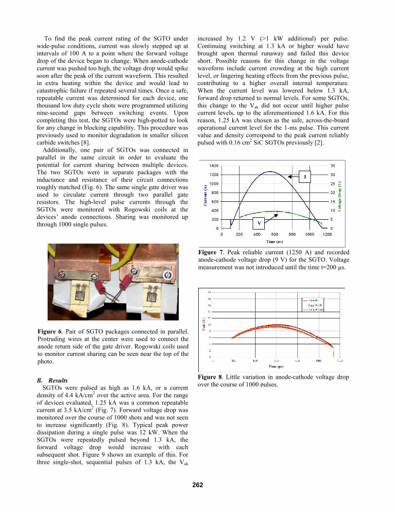
To find the peak current rating of the SGTO underwide-pulse conditions, current was slowly stepped up atintervals of 100 A to a point where the forward voltagedrop of the device began to change. When anode-cathodecurrent was pushed too high, the voltage drop would spikesoon after the peak of the current waveform. This resultedin extra heating within the device and would lead tocatastrophic failure if repeated several times. Once a safe,repeatable current was determined for each device, onethousand low duty cycle shots were programmed utilizingnine-second gaps between switching events. Uponcompleting this test, the SGTOs were high-potted to lookfor any change in blocking capability. This procedure waspreviously used to monitor degradation in smaller siliconcarbide switches [8].
Additionally, one pair of SGTOs was connected inparallel in the same circuit in order to evaluate thepotential for current sharing between multiple devices.The two SGTOs were in separate packages with theinductance and resistance of their circuit connectionsroughly matched (Fig. 6). The same single gate driver wasused to circulate current through two parallel gateresistors. The high-level pulse currents through theSGTOs were monitored with Rogowski coils at thedevices’ anode connections. Sharing was monitored upthrough 1000 single pulses.
B. ResultsSGTOs were pulsed as high as 1.6 kA, or a current
density of 4.4 kA/cm2 over the active area. For the rangeof devices evaluated, 1.25 kA was a common repeatablecurrent at 3.5 kA/cm2 (Fig. 7). Forward voltage drop wasmonitored over the course of 1000 shots and was not seento increase significantly (Fig. 8). Typical peak powerdissipation during a single pulse was 12 kW. When theSGTOs were repeatedly pulsed beyond 1.3 kA, theforward voltage drop would increase with eachsubsequent shot. Figure 9 shows an example of this. Forthree single-shot, sequential pulses of 1.3 kA, the Vak
increased by 1.2 V (>1 kW additional) per pulse.Continuing switching at 1.3 kA or higher would havebrought upon thermal runaway and failed this deviceshort. Possible reasons for this change in the voltagewaveform include current crowding at the high currentlevel, or lingering heating effects from the previous pulse,contributing to a higher overall internal temperature.When the current level was lowered below 1.3 kA,forward drop returned to normal levels. For some SGTOs,this change to the Vak did not occur until higher pulsecurrent levels, up to the aforementioned 1.6 kA. For thisreason, 1.25 kA was chosen as the safe, across-the-boardoperational current level for the 1-ms pulse. This currentvalue and density correspond to the peak current reliablypulsed with 0.16 cm2 SiC SGTOs previously [2].
Figure 6. Pair of SGTO packages connected in parallel.Protruding wires at the center were used to connect theanode return side of the gate driver. Rogowski coils usedto monitor current sharing can be seen near the top of thephoto.
Figure 7. Peak reliable current (1250 A) and recordedanode-cathode voltage drop (9 V) for the SGTO. Voltagemeasurement was not introduced until the time t=200 µs.
Figure 8. Little variation in anode-cathode voltage dropover the course of 1000 pulses.
I
V
262

The paralleled SGTOs shared gate current and cathodecurrent well. The original gate current of 1.2 A was splitbetween the two devices’ gates. At the peak of thecathode current pulse, each device carried ± 10 A, orwithin 1% of ideal, even current sharing (Fig. 10). Thetotal current output was 2.5 kA. This pair of SGTOs wasswitched 1000 times without any change in currentsharing.
C. Further TestingSilicon Power Corp. is directing assembly of four-chip
SGTO modules for further parallel device switching.Groups of four SGTOs will share a common cathode plateand utilize Silicon Power’s ThinPak lid rather than wirebonds. These modules will be used to verify packagingperformance and parallel integration of several SGTOs.The modules are expected to block greater than 5 kV andswitch about 5 kA of current. Information garnered fromthis portion of the study will aid the follow-ondevelopment of larger, higher current silicon carbideSGTO modules using the current silicon SGTO hardware.
IV. SUMMARY
Silicon carbide SGTOs fabricated at 0.5 cm2 die areawere switched up to 1.25 kA at a 1-ms wide pulse width.SGTOs were pulsed over 1000 times without increase inforward voltage drop or signs of degradation. Pairs ofdevices were also switches in parallel and demonstratedcurrent sharing within 1% of ideal sharing. Currentdivision remained consistent through 1000 switchingevents. These results suggest that six of these 0.5 cm2
SGTO could replace one current-generation 3.5 cm2
silicon SGTO and carry 40% more current and handlemore than twice the action in a smaller footprint. Theresults support further development of larger area, highervoltage silicon carbide SGTOs to meet the Army’s pulsedpower switching needs.
V. REFERENCES
[1] M. J. O’Loughlin, et al, “Silicon Carbide Hot-WallEpitaxy for Large-Area, High-Voltage Devices,”Materials Research Society Symp. Proc., vol. 1069,Spring 2008.[2] H. O’Brien, W. Shaheen, V. Chiscop, C. J. Scozzieand M. G. Koebke, “Evaluation of Si and SiC SGTOs forHigh-Action Army Applications,” IEEE Trans.Magnetics, vol. 45, no. 1, pp. 402-406, Jan. 2009.[3] “SiC Physical & Electronic Properties,” Cree, Inc.,Durham, NC, [Online], 2009 [cited June 2009], Available:http://www.cree.com Directory: products File:sic_sub_prop.asp[4] A. Agarwal, Q. Zhang, A. Burk, R. Callanan, and S.Mazumder, “Prospects of Bipolar Power Devices inSilicon Carbide,” Proc. of the 34th Annual IEEE IECON,pp. 2879-2884, Nov. 2008.[5] T. Burke, K. Xie, H. Singh, T. Podlesak, J. Flemish, J.Carter, S. Schneider, and J. Zhao, “Silicon carbidethyristors for electric guns,” IEEE Trans. Magn., vol. 33,no. 1, pp.432-437, Jan. 1997.
[6] V. Temple, “ ‘Super’ GTO’s push the limits ofthyristor physics,” Proc. of the 35th IEEE PESC, pp. 604-610, June 2004.[7] A. Ogunniyi, H. O’Brien, W. Shaheen, C.J. Scozzie,and V. Temple, “Comparison of Recovery Time anddV/dt Immunity for Si and SiC SGTOs,” Proc. of the 17th
IEEE PPC, 30 June – 2 July 2009, Washington, D.C.[8] H. O’Brien, W. Shaheen, S. B. Bayne, “Evaluation of4 mm x 4 mm Silicon Carbide Thyristors,” IEEE Trans.Dielectrics and Electrical Insulation, vol. 14, no. 4, pp.986-993, Aug. 2007.
Figure 9. Vak rising when the current level was pushedtoo high (1300 A) for one of the SGTOs. Current wasreduced for subsequent pulses, and the Vak returned to itsoriginal relatively flat shape.
Figure 10. Overlying currents carried by two parallelSGTOs (identified as X6Y8 and X5Y6). Total combinedcurrent was 2.5 kA. Sharing was within ± 1%, with X6Y8peaking at 1.27 kA and X5Y6 peaking at 1.29 kA.
263