xcver: combinational verilog examples - digital design principles
TRANSCRIPT
Combinational Verilog Examples XCver–1
Supplementary material to accompany Digital Design Principles and Practices, Fourth Edition, by John F. Wakerly. ISBN 0-13-186389-4. 2006 Pearson Education, Inc., Upper Saddle River, NJ. All rights reserved.
This material is protected under all copyright laws as they currently exist. No portion of this material may be reproduced, in any form or by any means, without permission in writing by the publisher.
XCver: Combinational Verilog ExamplesThis section shows combinational design examples using Verilog.
XCver.1 Barrel ShifterA barrel shifter is a combinational logic circuit with n data inputs, n dataoutputs, and a set of control inputs that specify how to shift the data betweeninput and output. A barrel shifter that is part of a microprocessor CPU cantypically specify the direction of shift (left or right), the type of shift (circular,arithmetic, or logical), and the amount of shift (typically 0 to n – 1 bits, butsometimes 1 to n bits).
In this subsection we’ll look at the design of a 16-bit barrel shifter that doessix different types of shifts, as specified by a 3-bit shift-mode input C[2:0]. A4-bit shift-amount input S[3:0] specifies the amount of shift. For example, if Cspecifies a left-circular shift and the input word is ABCDEFGHIJKLMNOP(where each letter represents one bit), and S[3:0] is 0101 (5), then the outputword is FGHIJKLMNOPABCDE.
We show in Section XCbb.1 at DDPPonline how to build a simple barrelshifter using MSI building blocks; this circuit performed only left circular shifts.In Section XCabl.1, we show how to define a more capable barrel shifter usingABEL, but we also point out that PLDs are normally unsuitable for realizingbarrel shifters. In this section we’ll show how Verilog can be used to describeboth the behavior and structure of barrel shifters for FPGA or ASIC realization.
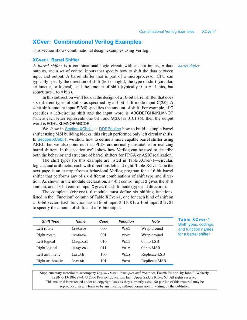
The shift types for this example are listed in Table XCver-1—circular,logical, and arithmetic, each with directions left and right. Table XCver-2 on thenext page is an excerpt from a behavioral Verilog program for a 16-bit barrelshifter that performs any of six different combinations of shift type and direc-tion. As shown in the module declaration, a 4-bit control input S gives the shiftamount, and a 3-bit control input C gives the shift mode (type and direction).
The complete Vrbarrel16 module must define six shifting functions,listed in the “Function” column of Table XCver-1, one for each kind of shift ona 16-bit vector. Each function has a 16-bit input D[15:0], a 4-bit input S[3:0]to specify the amount of shift, and a 16-bit output.
Shift Type Name Code Function Note Table XCver-1Shift types, codings, and function names for a barrel shifter.
Left rotate Lrotate 000 Vrol Wrap-around
Right rotate Rrotate 001 Vror Wrap-around
Left logical Llogical 010 Vsll 0 into LSB
Right logical Rlogical 011 Vslr 0 into MSB
Left arithmetic Larith 100 Vsla Replicate LSB
Right arithmetic Rarith 101 Vsra Replicate MSB
barrel shifter

Combinational Verilog Examples XCver–2
Supplementary material to accompany Digital Design Principles and Practices, Fourth Edition, by John F. Wakerly. ISBN 0-13-186389-4. 2006 Pearson Education, Inc., Upper Saddle River, NJ. All rights reserved.
This material is protected under all copyright laws as they currently exist. No portion of this material may be reproduced, in any form or by any means, without permission in writing by the publisher.
Table XCver-2 shows the details of only the first function (Vrol); the restare similar with only a one-line change (see Exercise XCver.1). We define aninteger variable ii for controlling the loop and a variable N to hold the integerequivalent of S for the loop-termination comparison. (See the box on page 333for an explanation of why we don’t like to use bit vectors like S in a for loop’scontrol statement.) The input vector D is assigned to a local variable TMPD,which is shifted N times within the for loop. The body of the for loop is just anassignment statement that concatenates the 15 rightmost bits of the input data(TMPD [14:0]) with the bit that “falls off” the left end in a left shift (TMPD[15]).
Table XCver-2 Verilog behavioral description of a 6-function barrel shifter.
module Vrbarrel16 (DIN, S, C, DOUT); input [15:0] DIN; // Data inputs input [3:0] S; // Shift amount, 0-15 input [2:0] C; // Mode control output [15:0] DOUT; // Data bus output reg [15:0] DOUT; parameter Lrotate = 3'b000, // Define the coding of Rrotate = 3'b001, // the different shift modes Llogical = 3'b010, Rlogical = 3'b011, Larith = 3'b100, Rarith = 3'b101;
function [15:0] Vrol; input [15:0] D; input [3:0] S; integer ii, N; reg [15:0] TMPD; begin N = S; TMPD = D; for (ii=1; ii<=N; ii=ii+1) TMPD = {TMPD[14:0], TMPD[15]}; Vrol = TMPD; end endfunction ...
always @ (DIN or S or C) case (C) Lrotate : DOUT = Vrol(DIN,S); Rrotate : DOUT = Vror(DIN,S); Llogical : DOUT = Vsll(DIN,S); Rlogical : DOUT = Vsrl(DIN,S); Larith : DOUT = Vsla(DIN,S); Rarith : DOUT = Vsra(DIN,S); default : DOUT = DIN; endcaseendmodule

Combinational Verilog Examples XCver–3
Supplementary material to accompany Digital Design Principles and Practices, Fourth Edition, by John F. Wakerly. ISBN 0-13-186389-4. 2006 Pearson Education, Inc., Upper Saddle River, NJ. All rights reserved.
This material is protected under all copyright laws as they currently exist. No portion of this material may be reproduced, in any form or by any means, without permission in writing by the publisher.
Other shift types can be created using similar operations in the five othershift functions. For some of the shift types, it is possible to use Verilog’s built-inshift operators (see Exercise XCver.2). Note that these six shift functions mightnot have to be defined in other, nonbehavioral versions of the Vrbarrel16module, such as the structural version that we’ll describe later.
After the function declarations, the rest of the module is a single alwaysblock that has all of the module’s inputs in its sensitivity list. Within the alwaysblock, a case statement assigns a result to DOUT by calling the appropriate shiftfunction based on the value of the mode-control input C.
The Verilog code in Table XCver-2 is a nice behavioral description of thebarrel shifter, but most synthesis tools cannot synthesize a circuit from it. Theproblem is that most tools require the range of a for loop to be static at the timeit is analyzed. The range of the for loop in the Vrol function is dynamic; itdepends on the value of input signal S when the circuit is operating.
Well, that’s OK; it’s hard to predict what kind of circuit the synthesis toolwould come up with even if it could handle a dynamic for range. This is anexample where we designers should take a little more control over the circuitstructure to obtain a reasonably fast, efficient synthesis result.
In Figure XCbb-2 in Section XCbb.1 we showed how to design a 16-bitbarrel shifter for left circular shifts using MSI building blocks. We used acascade of four 16-bit, 2-input multiplexers to shift their inputs by 0 or 1, 2, 4, or8 positions, depending on the values of S0 through S3, respectively. We canexpress the same kind of behavior and structure using the Verilog module shownin Table XCver-3. Even though this module uses an always block and is“behavioral” in style, we can be pretty sure that most synthesis tools willgenerate a 2-input multiplexer for each “if” statement in the program, therebycreating a cascade similar to Figure XCbb-2 in Section XCbb.1.
Table XCver-3 Verilog module for a 16-bit barrel shifter for left circular shifts only.
module Vrrol16 (DIN, S, DOUT); input [15:0] DIN; // Data inputs input [3:0] S; // Shift amount, 0-15 output [15:0] DOUT; // Data bus output reg [15:0] DOUT, X, Y, Z;
always @ (DIN or S) begin if (S[0] == 1'b1) X = {DIN[14:0], DIN[15]}; else X = DIN; if (S[1] == 1'b1) Y = {X[13:0], X[15:14]}; else Y = X; if (S[2] == 1'b1) Z = {Y[11:0], Y[15:12]}; else Z = Y; if (S[3] == 1'b1) DOUT = {Z[7:0], Z[15:8]}; else DOUT = Z; end
endmodule

Combinational Verilog Examples XCver–4
Supplementary material to accompany Digital Design Principles and Practices, Fourth Edition, by John F. Wakerly. ISBN 0-13-186389-4. 2006 Pearson Education, Inc., Upper Saddle River, NJ. All rights reserved.
This material is protected under all copyright laws as they currently exist. No portion of this material may be reproduced, in any form or by any means, without permission in writing by the publisher.
Of course, our problem statement requires a barrel shifter that can shiftboth left and right. Table XCver-4 revises the previous program to do circularshifts in either direction. An additional input, DIR, specifies the shift direction, 0for left, 1 for right. Each rank of shifting is specified by a case statement thatpicks one of four possibilities based on the values of DIR and the bit of S thatcontrols that rank.
A typical Verilog synthesis tool will generate a 3- or 4-input multiplexerfor each of the case statements in Table XCver-4. A good synthesis tool willgenerate only a 2-input multiplexer for the last case statement.
Table XCver-4 Verilog module for a 16-bit barrel shifter for left and right circular shifts.
module Vrrolr16 (DIN, S, DIR, DOUT); input [15:0] DIN; // Data inputs input [3:0] S; // Shift amount, 0-15 input DIR; // Shift direction, 0=>L, 1=>R output [15:0] DOUT; // Data bus output reg [15:0] DOUT, X, Y, Z;
always @ (DIN or S or DIR or X or Y or Z) begin case ( {S[0], DIR} ) 2'b00, 2'b01 : X = DIN; 2'b10 : X = {DIN[14:0], DIN[15]}; 2'b11 : X = {DIN[0], DIN[15:1]}; default : X = 16'bx; endcase
case ( {S[1], DIR} ) 2'b00, 2'b01 : Y = X; 2'b10 : Y = {X[13:0], X[15:14]}; 2'b11 : Y = {X[1:0], X[15:2]}; default : Y = 16'bx; endcase
case ( {S[2], DIR} ) 2'b00, 2'b01 : Z = Y; 2'b10 : Z = {Y[11:0], Y[15:12]}; 2'b11 : Z = {Y[3:0], Y[15:4]}; default : Z = 16'bx; endcase
case ( {S[3], DIR} ) 2'b00, 2'b01 : DOUT = Z; 2'b10, 2'b11 : DOUT = {Z[7:0], Z[15:8]}; default : DOUT = 16'bx; endcase endendmodule
Combinational Verilog Examples XCver–5
Supplementary material to accompany Digital Design Principles and Practices, Fourth Edition, by John F. Wakerly. ISBN 0-13-186389-4. 2006 Pearson Education, Inc., Upper Saddle River, NJ. All rights reserved.
This material is protected under all copyright laws as they currently exist. No portion of this material may be reproduced, in any form or by any means, without permission in writing by the publisher.
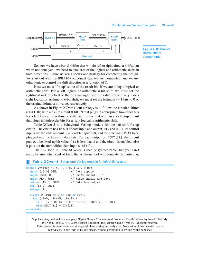
So, now we have a barrel shifter that will do left or right circular shifts, butwe’re not done yet—we need to take care of the logical and arithmetic shifts inboth directions. Figure XCver-1 shows our strategy for completing the design.We start out with the ROLR16 component that we just completed, and we useother logic to control the shift direction as a function of C.
Next we must “fix up” some of the result bits if we are doing a logical orarithmetic shift. For a left logical or arithmetic n-bit shift, we must set therightmost n–1 bits to 0 or the original rightmost bit value, respectively. For aright logical or arithmetic n-bit shift, we must set the leftmost n – 1 bits to 0 orthe original leftmost bit value, respectively.
As shown in Figure XCver-1, our strategy is to follow the circular shifter(ROLR16) with a fix-up circuit (FIXUP) that plugs in appropriate low-order bitsfor a left logical or arithmetic shift, and follow that with another fix-up circuitthat plugs in high-order bits for a right logical or arithmetic shift.
Table XCver-5 is a behavioral Verilog module for the left-shift fix-upcircuit. The circuit has 16 bits of data input and output, DIN and DOUT. Its controlinputs are the shift amount S, an enable input FEN, and the new value FDAT to beplugged into the fixed-up data bits. For each output bit DOUT[ii], the circuitputs out the fixed-up bit value if ii is less than S and the circuit is enabled; elseit puts out the unmodified data input DIN[ii].
The for loop in Table XCver-5 is readily synthesizable, but you can’treally be sure what kind of logic the synthesis tool will generate. In particular,
Table XCver-5 Behavioral Verilog module for left-shift fix-ups.
module Vrfixup (DIN, S, FEN, FDAT, DOUT); input [15:0] DIN; // Data inputs input [3:0] S; // Shift amount, 0-15 input FEN, FDAT; // Fixup enable and data output [15:0] DOUT; // Data bus output reg [15:0] DOUT; integer ii;
always @ (DIN or S or FEN or FDAT) for (ii=0; ii<=15; ii=ii+1) if ( (ii < S) && (FEN == 1'b1) ) DOUT[ii] = FDAT; else DOUT[ii] = DIN[ii];endmodule
FIXUP(left)
FIXUP(right)
ROUT(15:0) FOUT(15:0)DOUT(15:0)ROLR16
other logic
ROUT(0) FOUT(15)
DIN(15:0)
S(3:0)
C(2:0)
Figure XCver-1Barrel-shifter components.

Combinational Verilog Examples XCver–6
Supplementary material to accompany Digital Design Principles and Practices, Fourth Edition, by John F. Wakerly. ISBN 0-13-186389-4. 2006 Pearson Education, Inc., Upper Saddle River, NJ. All rights reserved.
This material is protected under all copyright laws as they currently exist. No portion of this material may be reproduced, in any form or by any means, without permission in writing by the publisher.
the “<” operation in each step of the loop may cause the synthesis of a general-purpose magnitude comparator, even though one of the operands is a constantand each output could therefore be generated with no more than a handful ofgates. (In fact, the logic for “7 < S” is just a wire, S[3]!) For a structural versionof this function, see the box at the top of this page.
For right shifts, fix-ups start from the opposite end of the data word, so itwould appear that we need a second version of the fix-up circuit. However, we
Table XCver-6 Structural Verilog module for left-shift fix-ups.
module Vrfixup_s (DIN, S, FEN, FDAT, DOUT); input [15:0] DIN; // Data inputs input [3:0] S; // Shift amount, 0-15 input FEN, FDAT; // Fixup enable and data output [15:0] DOUT; // Data bus output wire [15:0] DOUT, FSEL; // FSEL selects fixup or not per bit genvar ii;
assign FSEL[15] = 1'b0; assign DOUT[15] = DIN[15]; generate for (ii=14; ii>=0; ii=ii-1) begin : Fgen assign FSEL[ii] = (S==ii+1) ? 1'b1 : FSEL[ii+1]; assign DOUT[ii] = ((FSEL[ii] & FEN)==1'b1) ? FDAT : DIN[ii]; end endgenerateendmodule
A SERIAL FIX-UPSTRUCTURE
A structural module for the fix-up logic is shown in Table XCver-6. Here, we havedefined what is in effect an iterative circuit to create a 16-bit vector FSEL, whereFSEL[ii] is 1 if bit ii needs fixing up. We start by setting FSEL[15] to 0, since thatbit never needs fixing up. Then we note that for the remaining values of ii,FSEL[ii] should be 1 if S equals ii+1 or if FSEL[ii+1] is already asserted. Thus,the FSEL assignment within the generate for loop creates a serial chain of 2-inputOR gates, where one input is asserted if S=ii (decoded with a 4-input AND gate),and the other input is connected to the previous OR gate’s output. The DOUT[ii]assignment statement creates 16 2-input multiplexers that select either DIN[ii] orthe fix-up data (FDAT), depending on the value of FSEL[ii].
Although the serial realization is compact, it is very slow compared to one thatrealizes each FSEL output as a 2-level sum-of-products circuit. However, the longdelay may not matter, since the fix-up circuit appears near the end of the data path;FSEL need not be valid until the shifted data has made it through the ROLR16 module.If speed is still a problem, Exercise XCver.5 uses a zero-cost trick to cut the delay inhalf. Also, note that generate blocks are not available in Verilog-1995.

Combinational Verilog Examples XCver–7
Supplementary material to accompany Digital Design Principles and Practices, Fourth Edition, by John F. Wakerly. ISBN 0-13-186389-4. 2006 Pearson Education, Inc., Upper Saddle River, NJ. All rights reserved.
This material is protected under all copyright laws as they currently exist. No portion of this material may be reproduced, in any form or by any means, without permission in writing by the publisher.
can use the original version if we just reverse the order of its input and outputbits, as we’ll soon see.
Table XCver-7 is a structural Verilog module for the complete, 16-bit,6-function barrel shifter using the design approach of Figure XCver-1. Themodule inputs, output, and parameters for Vrbarrel16_s are unchanged fromthe original ones in Table XCver-2. The module instantiates Vrrolr16 and twocopies of Vrfixup and has several assignment statements that create neededcontrol signals (the “other logic” in Figure XCver-1).
The first assignment asserts DIR_RIGHT if C specifies one of the rightshifts. The next four assignments set the proper values for enable inputsFIX_LEFT and FIX_RIGHT and fix-up data FIX_LEFT_DAT and FIX_RIGHT_DATfor the left and right fix-up circuits, needed for logical and arithmetic shifts.
Table XCver-7 Verilog structural module for the 6-function barrel shifter.
module Vrbarrel16_s (DIN, S, C, DOUT); input [15:0] DIN; // Data inputs input [3:0] S; // Shift amount, 0-15 input [2:0] C; // Mode control output [15:0] DOUT; // Data bus output wire [15:0] DOUT; wire [15:0] ROUT, FOUT, RFIXIN, RFIXOUT; // Local wires wire DIR_RIGHT, FIX_RIGHT, FIX_RIGHT_DAT, FIX_LEFT, FIX_LEFT_DAT; genvar ii; parameter Lrotate = 3'b000, // Define the coding of Rrotate = 3'b001, // the different shift modes Llogical = 3'b010, Rlogical = 3'b011, Larith = 3'b100, Rarith = 3'b101;
assign DIR_RIGHT = ( (C==Rrotate) || (C==Rlogical) || (C==Rarith) ) ? 1'b1 : 1'b0; assign FIX_LEFT = ( (DIR_RIGHT==1'b0) && ((C==Llogical)||(C==Larith)) ) ? 1'b1 : 1'b0; assign FIX_RIGHT = ( (DIR_RIGHT==1'b1) && ((C==Rlogical)||(C==Rarith)) ) ? 1'b1 : 1'b0; assign FIX_LEFT_DAT = (C == Larith) ? DIN[0] : 1'b0; assign FIX_RIGHT_DAT = (C == Rarith) ? DIN[15] : 1'b0; Vrrolr16 U1 ( .DIN(DIN), .S(S), .DIR(DIR_RIGHT), .DOUT(ROUT) ); Vrfixup U2 ( .DIN(ROUT), .S(S), .FEN(FIX_LEFT), .FDAT(FIX_LEFT_DAT), .DOUT(FOUT) ); generate for (ii=0; ii<=15; ii=ii+1) begin : U3 assign RFIXIN[ii] = FOUT[15-ii]; end endgenerate Vrfixup U4 ( .DIN(RFIXIN),.S(S),.FEN(FIX_RIGHT),.FDAT(FIX_RIGHT_DAT),.DOUT(RFIXOUT) ); generate for (ii=0; ii<=15; ii=ii+1) begin : U5 assign DOUT[ii] = RFIXOUT[15-ii]; end endgenerateendmodule
Combinational Verilog Examples XCver–8
Supplementary material to accompany Digital Design Principles and Practices, Fourth Edition, by John F. Wakerly. ISBN 0-13-186389-4. 2006 Pearson Education, Inc., Upper Saddle River, NJ. All rights reserved.
This material is protected under all copyright laws as they currently exist. No portion of this material may be reproduced, in any form or by any means, without permission in writing by the publisher.
While all the statements in the module execute concurrently, they are listedin Table XCver-7 in the order of the actual dataflow to improve readability. First,Vrrolr16 (U1) is instantiated to perform the basic left or right circular shift asspecified. Its outputs are hooked up to the inputs of the first Vrfixup component(U2) to handle fix-ups for left logical and arithmetic shifts. Next is a generateblock that reverses the order of the data inputs for the next fixup component(U4), which handles fix-ups for right logical and arithmetic shifts. The finalgenerate block undoes the previous bit-reversing. Note that in synthesis, the twogenerate blocks don’t generate any logic; they merely shuffle wires.
Many other design approaches are possible for the original Vrbarrel16module. For example, in Exercise XCver.6, we suggest an approach that allowsthe shifting to be done by the Vrrol16 module, which uses only 2-input multi-plexers, rather than the more expensive Vrrolr16.
XCver.2 Simple Floating-Point EncoderAn unsigned binary integer B in the range 0 ≤ B < 211 can be represented by 11bits in “fixed-point” format, B = b10b9…b1b0. We can represent numbers inthe same range with less precision using only 7 bits in a floating-point notation,F = M ⋅ 2E, where M is a 4-bit mantissa m3m2m1m0 and E is a 3-bit exponente2e1e0. The smallest integer in this format is 0⋅20 and the largest is (24−1) ⋅ 27.
Given an 11-bit fixed-point integer B, we can convert it to our 7-bitfloating-point notation by “picking off” four high-order bits beginning with themost significant 1, for example,
11010110100 = 1101 ⋅ 27 + 0110100
00100101111 = 1001 ⋅ 25 + 01111
00000111110 = 1111 ⋅ 22 + 10
00000001011 = 1011 ⋅ 20 + 0
00000000010 = 0010 ⋅ 20 + 0
INFORMATION-HIDING STYLE
Based on the encoding of C, you might like to replace the first assignment statementin Table XCver-7 with “DIR_RIGHT <= C[0]”, which would be guaranteed to lead toa more efficient realization for that control bit—just a wire! However, this wouldviolate a programming principle of information hiding and lead to possible bugs.
We explicitly wrote the shift encodings using parameter definitions in theVrbarrel16 module declaration. The rest of the module does not depend on theencoding details. Suppose that we nevertheless made the architecture change sug-gested above. If somebody else (or we!) came along later and changed theparameter definitions to a different encoding, the rest of the module would not usethe new encodings!

Combinational Verilog Examples XCver–9
Supplementary material to accompany Digital Design Principles and Practices, Fourth Edition, by John F. Wakerly. ISBN 0-13-186389-4. 2006 Pearson Education, Inc., Upper Saddle River, NJ. All rights reserved.
This material is protected under all copyright laws as they currently exist. No portion of this material may be reproduced, in any form or by any means, without permission in writing by the publisher.
The last term in each equation is a truncation error that results from the loss ofprecision in the conversion. Corresponding to this conversion operation, we canwrite the specification for a fixed-point to floating-point encoder circuit:
• A combinational circuit is to convert an 11-bit unsigned binary integer B intoa 7-bit floating-point number M,E, where M and E have 4 and 3 bits,respectively. The numbers have the relationship B = M ⋅2E + T, where T isthe truncation error, 0 ≤ T < 2E.
As shown in Section XCbb, the problem of determining the exponent ofthe floating-point number maps nicely into an MSI priority encoder and multi-plexers. In an HDL, the same problem maps into nested “if” statements.
Table XCver-8 is a behavioral Verilog module for the floating-pointencoder. Within the always block, a nested “if” statement checks the range ofthe input B and assigns the values of outputs M and E appropriately.
Although the code in Table XCver-8 is fully synthesizable, some synthesistools may not be smart enough to recognize that the nested comparisons requirejust one bit to be checked at each level, and might instead generate a full 11-bitcomparator at each level. Such logic would be a lot bigger and slower than whatotherwise would be possible. If faced with this problem, we can always write themodule a little differently and more explicitly to help out the tool, as shown inTable XCver-9.
On the other hand, we might like to use real comparators and spend evenmore gates to improve the functionality of our design. In particular, the presentdesign performs truncation rather than rounding when generating the mantissabits. A more accurate result is achieved with rounding, but this is a much morecomplicated design. First, we will need an adder to add 1 to the selected mantis-sa bits when we round up. However, adding 1 when the mantissa is already 1111
module fpenc (B, M, E); input [10:0] B; // fixed-point number output [3:0] M; // floating-point mantissa output [2:0] E; // floating-point exponent reg [3:0] M; reg [2:0] E;
always @ (B) if (B < 16) begin M = B[3:0]; E = 3'b000; end else if (B < 32) begin M = B[4:1]; E = 3'b001; end else if (B < 64) begin M = B[5:2]; E = 3'b010; end else if (B < 128) begin M = B[6:3]; E = 3'b011; end else if (B < 256) begin M = B[7:4]; E = 3'b100; end else if (B < 512) begin M = B[8:5]; E = 3'b101; end else if (B < 1024) begin M = B[9:6]; E = 3'b110; end else begin M = B[10:7]; E = 3'b111; endendmodule
Table XCver-8Behavioral Verilog module for fixed-point to floating-point conversion.
Combinational Verilog Examples XCver–10
Supplementary material to accompany Digital Design Principles and Practices, Fourth Edition, by John F. Wakerly. ISBN 0-13-186389-4. 2006 Pearson Education, Inc., Upper Saddle River, NJ. All rights reserved.
This material is protected under all copyright laws as they currently exist. No portion of this material may be reproduced, in any form or by any means, without permission in writing by the publisher.
will bump us into the next exponent range, so we need to watch out for this case.Finally, we can never round up if the unrounded mantissa and exponent are 1111and 111, because there’s no higher value in our floating-point representation.
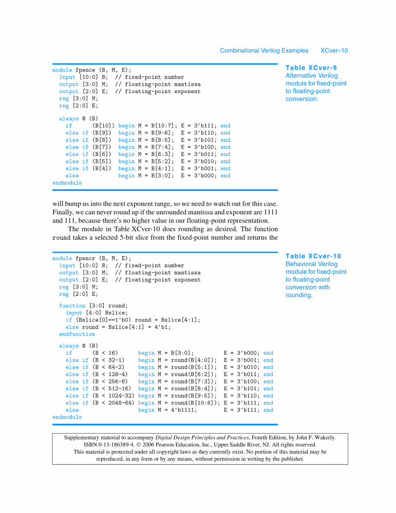
The module in Table XCver-10 does rounding as desired. The functionround takes a selected 5-bit slice from the fixed-point number and returns the
module fpence (B, M, E); input [10:0] B; // fixed-point number output [3:0] M; // floating-point mantissa output [2:0] E; // floating-point exponent reg [3:0] M; reg [2:0] E;
always @ (B) if (B[10]) begin M = B[10:7]; E = 3'b111; end else if (B[9]) begin M = B[9:6]; E = 3'b110; end else if (B[8]) begin M = B[8:5]; E = 3'b101; end else if (B[7]) begin M = B[7:4]; E = 3'b100; end else if (B[6]) begin M = B[6:3]; E = 3'b011; end else if (B[5]) begin M = B[5:2]; E = 3'b010; end else if (B[4]) begin M = B[4:1]; E = 3'b001; end else begin M = B[3:0]; E = 3'b000; endendmodule
Table XCver-9Alternative Verilog module for fixed-point to floating-point conversion.
module fpencr (B, M, E); input [10:0] B; // fixed-point number output [3:0] M; // floating-point mantissa output [2:0] E; // floating-point exponent reg [3:0] M; reg [2:0] E;
function [3:0] round; input [4:0] Bslice; if (Bslice[0]==1'b0) round = Bslice[4:1]; else round = Bslice[4:1] + 4'b1; endfunction
always @ (B) if (B < 16) begin M = B[3:0]; E = 3'b000; end else if (B < 32-1) begin M = round(B[4:0]); E = 3'b001; end else if (B < 64-2) begin M = round(B[5:1]); E = 3'b010; end else if (B < 128-4) begin M = round(B[6:2]); E = 3'b011; end else if (B < 256-8) begin M = round(B[7:3]); E = 3'b100; end else if (B < 512-16) begin M = round(B[8:4]); E = 3'b101; end else if (B < 1024-32) begin M = round(B[9:5]); E = 3'b110; end else if (B < 2048-64) begin M = round(B[10:6]); E = 3'b111; end else begin M = 4'b1111; E = 3'b111; endendmodule
Table XCver-10Behavioral Verilog module for fixed-point to floating-point conversion with rounding.

Combinational Verilog Examples XCver–11
Supplementary material to accompany Digital Design Principles and Practices, Fourth Edition, by John F. Wakerly. ISBN 0-13-186389-4. 2006 Pearson Education, Inc., Upper Saddle River, NJ. All rights reserved.
This material is protected under all copyright laws as they currently exist. No portion of this material may be reproduced, in any form or by any means, without permission in writing by the publisher.
four high-order bits, adding 1 if the LSB is 1. Thus, if we think of the binarypoint as being just to the left of the LSB, rounding occurs if the truncated part ofthe mantissa is 1/2 or more. In each clause in the nested “if” statement in theprocess, the comparison value is selected so that rounding up will occur only if itdoes not “overflow,” pushing the result into the next exponent range. Otherwise,conversion and rounding occurs in the next clause. In the last clause, we ensurethat we do not round up when we’re at the end of the floating-point range.
NO HELP NEEDED Some synthesis tools and environments don’t need any help to get a “minimal”realization of the floating-point encoder or any other moderately sized circuit.
In particular, consider the situation when the design is targeted to a CPLD,such as the Xilinx XC9500 family. The synthesis tool may come up with a structurethat includes multiple comparators and adders—expensive. For example, when yousynthesize the Vrfpencr module of Table XCver-10 using the Xilinx ISE tools, youcan use ISE’s “RTL schematic viewer” to see the synthesized structure. It’s prettyscary, including eight adders and a serial realization of the multiplexing function thatselects the mantissa bits.
But when this structure is handed over to the fitter to target an XC9500 CPLD,the fitter flattens the entire design, since it has to derive a two-level sum-of-productsexpression for each of the circuit’s seven outputs. Then it minimizes these expres-sions, with the result that 89 product terms are needed for the entire realization.
Still, the rounding module in Table XCver-10 is more expensive than the non-rounding ones in Tables XCver-8 and XCver-9, which require only 33 product termseach (the same ones in both designs, by the way).
GOBBLE,GOBBLE
Let’s continue the discussion from the previous box. Even in environments where thefitter does not flatten the design and minimize equations, a sophisticated synthesistool can still save gates. For example, the rounding operation in Table XCver-10does not require a 4-bit adder, only an “incrementer,” since one of the addends isalways 1. Some tools are smart enough to synthesize an incrementer with far fewergates than an adder.
Even if an adder is synthesized, it still may not matter. The most sophisticatedtools for FPGA and ASIC design include gate gobblers. These programs look forgates with constant inputs and eliminate gates or gate inputs as a result. For example,an AND-gate input with a constant 1 applied to it can be eliminated, and an AND gatewith a constant-0 input can be replaced with a constant-0 signal.
A gate-gobbler program propagates the effects of constant inputs as far aspossible in a circuit. Thus, it can transform a 4-bit adder with a constant-0001 addendinput into a more economical 4-bit incrementer.

Combinational Verilog Examples XCver–12
Supplementary material to accompany Digital Design Principles and Practices, Fourth Edition, by John F. Wakerly. ISBN 0-13-186389-4. 2006 Pearson Education, Inc., Upper Saddle River, NJ. All rights reserved.
This material is protected under all copyright laws as they currently exist. No portion of this material may be reproduced, in any form or by any means, without permission in writing by the publisher.
Once again, synthesis results for this behavioral program may or may notbe efficient. Besides the multiple comparison statements, we now must worryabout the multiple 4-bit adders that might be synthesized as a result of themultiple calls to the round function. Restructuring the module so that only asingle adder is synthesized is left as an exercise (XCver.8).
XCver.3 Dual-Priority EncoderIn this example, we’ll use Verilog to create a behavioral description of a priorityencoder that identifies both the highest-priority and the second-highest-priorityasserted signal among a set of request inputs R[0:7], where R[0] has thehighest priority. We’ll use outputs A[2:0] and AVALID to identify the highest-priority request, asserting AVALID only if a highest-priority request is present.Similarly, we’ll use outputs B[2:0] and BVALID to identify the second-highest-priority request.
Table XCver-11 is a behavioral Verilog module for the priority encoder.Instead of the nested “if” approach of the previous example, we’ve used a“for” loop. This approach allows us to take care of both the first and the secondpriorities within the same loop, working our way from highest to lowest priority.
The nested “if” approach can also be used for the dual-priority encoder,but it yields a longer program with more accidents waiting to happen, as shownin Table XCver-12 on the next page. On the other hand, it may yield a bettersynthesis result; the only way to know with a particular tool is to synthesize thecircuit and analyze the results in terms of delay and cell or gate count.
Both nested “if” statements and “for” statements may lead to long delaychains in synthesis. To guarantee that you get a faster dual-priority encoder, youmust follow a structural or semistructural design approach. For example, youcan start by writing a dataflow model of a fast 8-input priority encoder using theideas found in the 74x148 logic diagram (at DDPPonline in Section Enc) or in a
module Vrprior2 ( R, A, B, AVALID, BVALID ); input [0:7] R; output [2:0] A, B; output AVALID, BVALID; reg [2:0] A, B; reg AVALID, BVALID; integer ii;
always @ (R) begin AVALID = 1'b0; BVALID = 1'b0; A = 3'b000; B = 3'b000; for (ii=0; ii<=7; ii=ii+1) if (R[ii] & ~AVALID) begin A = ii; AVALID = 1'b1; end else if (R[ii] & ~BVALID) begin B = ii; BVALID = 1'b1; end endendmodule
Table XCver-11Behavioral Verilog module for a dual-priority encoder.

Combinational Verilog Examples XCver–13
Supplementary material to accompany Digital Design Principles and Practices, Fourth Edition, by John F. Wakerly. ISBN 0-13-186389-4. 2006 Pearson Education, Inc., Upper Saddle River, NJ. All rights reserved.
This material is protected under all copyright laws as they currently exist. No portion of this material may be reproduced, in any form or by any means, without permission in writing by the publisher.
related ABEL program (Table 6-28 on page 414). Then you can put two of thesetogether in a structure that “knocks out” the highest-priority input in orderto find the second, as we did with MSI building blocks in Figure XCbb-5 inSection XCbb.3.
XCver.4 Cascading ComparatorsCascading comparators is something we typically would not do in a Verilogbehavioral design, because the language lets us define comparators of anydesired length directly. However, we may indeed need to write structural orsemistructural Verilog modules that hook up smaller comparator components ina specific way to obtain high performance.
A very simple Verilog dataflow design for a 64-bit comparator with equalsand greater-than outputs is shown in Table XCver-13. Although the module isfully synthesizable, the speed and size of the result depends on the “intelligence”of the particular synthesis tool that is used.
An alternative is to build the comparator by cascading smaller components,such as 8-bit comparators. Table XCver-14 is the same module with definitionchanges for an 8-bit comparator. A particular tool may or may not synthesize a
Table XCver-12 Alternative Verilog module for a dual-priority encoder.
module Vrprior2i ( R, A, B, AVALID, BVALID ); input [0:7] R; output [2:0] A, B; output AVALID, BVALID; reg [2:0] A, B; reg AVALID, BVALID;
always @ (R or A) begin if (R[0]) begin A = 3'b000; AVALID = 1'b1; end else if (R[1]) begin A = 3'b001; AVALID = 1'b1; end else if (R[2]) begin A = 3'b010; AVALID = 1'b1; end else if (R[3]) begin A = 3'b011; AVALID = 1'b1; end else if (R[4]) begin A = 3'b100; AVALID = 1'b1; end else if (R[5]) begin A = 3'b101; AVALID = 1'b1; end else if (R[6]) begin A = 3'b110; AVALID = 1'b1; end else if (R[7]) begin A = 3'b111; AVALID = 1'b1; end else begin A = 3'b000; AVALID = 1'b0; end if (R[1] && (A != 3'b001)) begin B = 3'b001; BVALID = 1'b1; end else if (R[2] && (A != 3'b010)) begin B = 3'b010; BVALID = 1'b1; end else if (R[3] && (A != 3'b011)) begin B = 3'b011; BVALID = 1'b1; end else if (R[4] && (A != 3'b100)) begin B = 3'b100; BVALID = 1'b1; end else if (R[5] && (A != 3'b101)) begin B = 3'b101; BVALID = 1'b1; end else if (R[6] && (A != 3'b110)) begin B = 3'b110; BVALID = 1'b1; end else if (R[7] && (A != 3'b111)) begin B = 3'b111; BVALID = 1'b1; end else begin B = 3'b000; BVALID = 1'b0; end end

Combinational Verilog Examples XCver–14
Supplementary material to accompany Digital Design Principles and Practices, Fourth Edition, by John F. Wakerly. ISBN 0-13-186389-4. 2006 Pearson Education, Inc., Upper Saddle River, NJ. All rights reserved.
This material is protected under all copyright laws as they currently exist. No portion of this material may be reproduced, in any form or by any means, without permission in writing by the publisher.
very fast comparator from this program, but it’s sure to be significantly fasterthan a 64-bit comparator in any case.
Next, we can write a structural module that instantiates eight of these 8-bitcomparators and hooks up their individual outputs through additional logic tocalculate the overall 64-bit comparison result. One way to do this is shownTable XCver-15. A Verilog-2001 generate block creates the individual 8-bitcomparators and cascading logic that serially builds up the overall result fromthe most significant to the least significant stage.
An unsophisticated tool might synthesize a slow iterative comparatorcircuit from our original 64-bit comparator design in Table XCver-13. With sucha synthesizer, the design in Table XCver-15 can lead to a faster circuit because
module Vrcomp64 ( A, B, EQ, GT ); input [63:0] A, B; output EQ, GT;
assign EQ = (A == B) ? 1'b1 : 1'b0 ; assign GT = (A > B) ? 1'b1 : 1'b0 ;endmodule
Table XCver-13Dataflow Verilog module for a 64-bit comparator.
module Vrcomp8 ( A, B, EQ, GT ); input [7:0] A, B; output EQ, GT;
assign EQ = (A == B) ? 1'b1 : 1'b0 ; assign GT = (A > B) ? 1'b1 : 1'b0 ;endmodule
Table XCver-14Dataflow Verilog module for an 8-bit comparator.
Table XCver-15 Verilog structural module for a 64-bit comparator.
module Vrcomp64_s ( A, B, EQ, GT ); input [63:0] A, B; output EQ, GT; wire [7:0] EQ8, GT8; // = and > for 8-bit bytes wire [8:0] SEQ, SGT; // serial chain of byte results genvar ii; // loop control for generate
assign SEQ[8] = 1'b1; assign SGT[8] = 1'b0; generate for (ii=7; ii>=0; ii=ii-1) begin : G Vrcomp8 U1 ( .A( A[7+ii*8 : ii*8] ), .B( B[7+ii*8:ii*8] ), .EQ(EQ8[ii]), .GT(GT8[ii]) ); assign SEQ[ii] = SEQ[ii+1] & EQ8[ii]; assign SGT[ii] = SGT[ii+1] | (SEQ[ii+1] & GT8[ii]); end endgenerate assign EQ = SEQ[0]; assign GT = SGT[0];endmodule

Combinational Verilog Examples XCver–15
Supplementary material to accompany Digital Design Principles and Practices, Fourth Edition, by John F. Wakerly. ISBN 0-13-186389-4. 2006 Pearson Education, Inc., Upper Saddle River, NJ. All rights reserved.
This material is protected under all copyright laws as they currently exist. No portion of this material may be reproduced, in any form or by any means, without permission in writing by the publisher.
the design explicitly “pulls out” the cascading information for each 8-bit byteand combines it in a faster combinational circuit (just 8 levels of AND-OR logic,not 64). A more sophisticated synthesizer might flatten the 8-bit comparatorinto a faster, noniterative structure similar to the 74x682 MSI comparator(Figure 6-82 on page 464), and it might flatten our iterative cascading logic inTable XCver-15 into two-level sum-of-products equations similar to the ones inthe ABEL solution in Table XCabl-7 in Section XCabl.4.
XCver.5 Mode-Dependent ComparatorFor the next example, let us suppose we have a system in which we need to com-pare two 32-bit words under normal circumstances, but where we mustsometimes ignore one or two low-order bits of the input words. The operatingmode of the comparator is specified by two mode-control bits, M1 and M0, asshown in Table XCver-16.
The desired functionality can be obtained very easily in Verilog using acase statement to select the behavior by mode, as shown in the module inTable XCver-17. This is a perfectly good behavioral description that is also fullysynthesizable. However, it has one major drawback in synthesis—it will, in alllikelihood, cause the creation of three separate equality and magnitudecomparators (32-, 31-, and 30-bit), one for each case in the case statement. Theindividual comparators may or may not be fast, as discussed in the previoussubsection, but we won’t worry about speed for this example.
M1 M0 Comparison Table XCver-16Mode-control bits for the mode-dependent comparator.
0 0 32-bit0 1 31-bit1 0 30-bit1 1 not used
THE RESULTSSPEAK FOR
THEMSELVES
Using the Xilinx ISE tools, I targeted both 64-bit comparator modules on the previ-ous page to the XC9500 CPLD family. I set the fitter to “optimize balance,” that is,to try to achieve a balance between speed and cost, rather than minimizing speed atthe cost of more product terms, or minimizing product terms but reducing speed(typically by cascading).
The simple Vrcomp64 module in Table XCver-13 required 408 product termsin an XC95144-7 CPLD, and its worst input-to-output paths had a propagation delayof 42 ns. The structural Vrcomp64_s module in Table XCver-15 required only 328product terms in the same CPLD, and its worst input-to-output paths had a delay ofonly 31.5 ns.

Combinational Verilog Examples XCver–16
Supplementary material to accompany Digital Design Principles and Practices, Fourth Edition, by John F. Wakerly. ISBN 0-13-186389-4. 2006 Pearson Education, Inc., Upper Saddle River, NJ. All rights reserved.
This material is protected under all copyright laws as they currently exist. No portion of this material may be reproduced, in any form or by any means, without permission in writing by the publisher.
A more efficient alternative is to perform just one comparison for the 30high-order bits of the inputs, and to use additional logic that is dependent onmode to give a final result using the low-order bits as necessary. This approach isshown in Table XCver-18 on the next page. Two variables, EQ30 and GT30, areused within the process to hold the results of the comparison of the 30 high-orderbits. A case statement similar to the previous module’s is then used to obtain thefinal results as a function of the mode. If desired, the speed of the 30-bit compar-ison can be optimized using the methods discussed in the preceding subsection.
module Vrmodecmp ( M, A, B, EQ, GT ); input [1:0] M; input [31:0] A, B; output EQ, GT; reg EQ, GT; parameter M32bit = 2'b00, // Define comparison modes M31bit = 2'b01, M30bit = 2'b10, Mxtra = 2'b11;
always @ (M or A or B) begin case (M) M32bit : begin if (A == B) EQ = 1'b1; else EQ = 1'b0; if (A > B) GT = 1'b1; else GT = 1'b0; end M31bit : begin if (A[31:1] == B[31:1]) EQ = 1'b1; else EQ = 1'b0; if (A[31:1] > B[31:1]) GT = 1'b1; else GT = 1'b0; end M30bit : begin if (A[31:2] == B[31:2]) EQ = 1'b1; else EQ = 1'b0; if (A[31:2] > B[31:2]) GT = 1'b1; else GT = 1'b0; end default : begin EQ = 1'b0; GT = 1'b0; end endcase endendmodule
Table XCver-17Verilog behavioral module for a 32-bit mode-dependent comparator.
INTELLIGENTCODING WINS
AGAIN
Using the same setup as in the previous box, I targeted both mode-dependentcomparator modules to the XC9500 CPLD family. The Vrmodecmp module inTable XCver-17 required 456 product terms in an XC95144-7 CPLD, and its worstinput-to-output paths had a propagation delay of 33.5 ns. The “efficient” alternative,Vrmodecompe in Table XCver-18, was not much faster at 32.5 ns. But it requiredonly 211 product terms, easily fitting into the smaller and cheaper XC95108-7.

Combinational Verilog Examples XCver–17
Supplementary material to accompany Digital Design Principles and Practices, Fourth Edition, by John F. Wakerly. ISBN 0-13-186389-4. 2006 Pearson Education, Inc., Upper Saddle River, NJ. All rights reserved.
This material is protected under all copyright laws as they currently exist. No portion of this material may be reproduced, in any form or by any means, without permission in writing by the publisher.
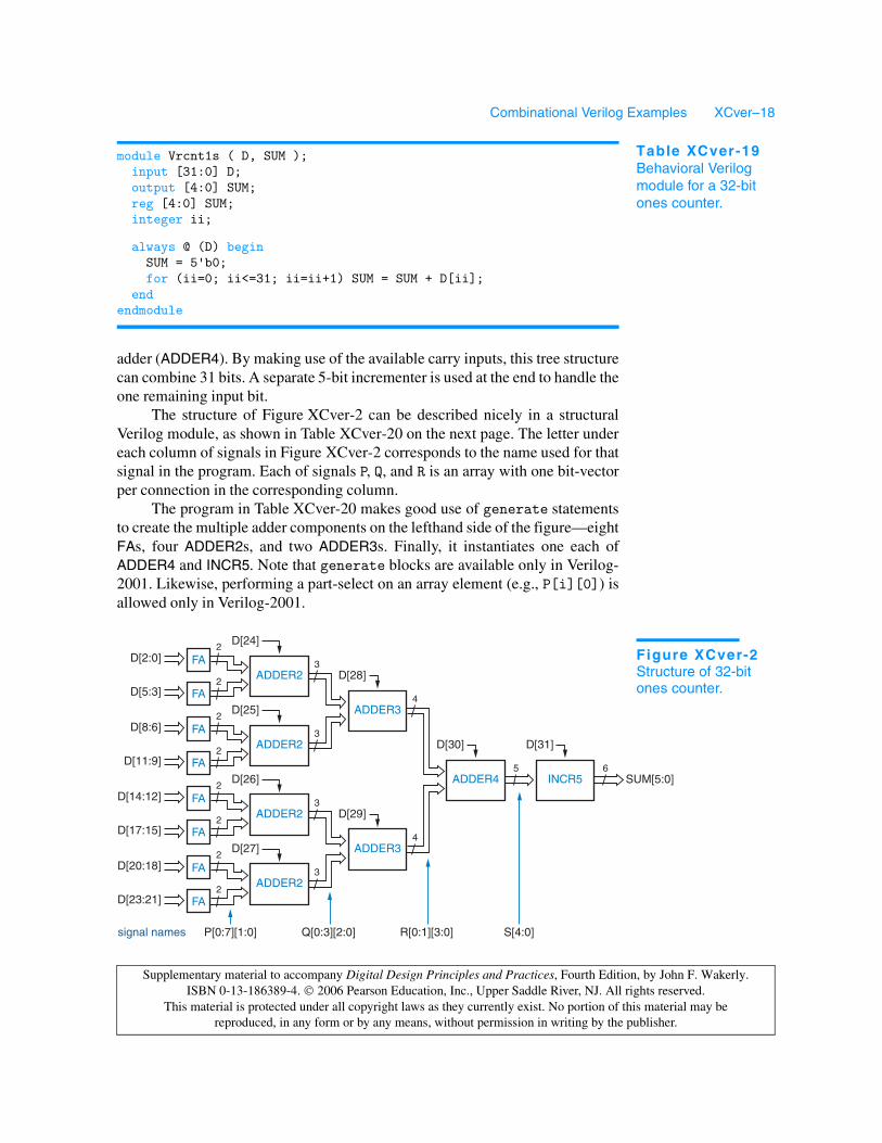
XCver.6 Ones CounterSeveral important algorithms include the step of counting the number of “1” bitsin a data word. In fact, some microprocessor instruction sets have been extendedto include ones counting as a basic instruction. In this example, let us supposethat we have a requirement to design a combinational circuit that counts ones ina 32-bit word as part of the arithmetic and logic unit of a microprocessor.
Ones counting can be described very easily by a behavioral Verilogmodule, as shown in Table XCver-19. This module is fully synthesizable, but itmay generate a very large, slow realization with 32 5-bit adders in series.
To synthesize a more efficient realization of the ones counter, we shouldcome up with an efficient structure and then write structural Verilog code thatdescribes it. Such a structure is the adder tree shown in Figure XCver-2. A fulladder (FA) adds three input bits to produce a 2-bit sum. Pairs of 2-bit numbersare added by 2-bit adders (ADDER2), each of which also has a carry input thatcan add another 1-bit input to its sum. The resulting 3-bit sums are combined by3-bit adders (ADDER3), and the final pair of 4-bit sums are combined in a 4-bit
Table XCver-18 More efficient module for a 32-bit mode-dependent comparator.
module Vrmodecmpe ( M, A, B, EQ, GT ); input [1:0] M; input [31:0] A, B; output EQ, GT; reg EQ, GT; reg EQ30, GT30; // 30-bit comparison results parameter M32bit = 2'b00, // Define comparison modes M31bit = 2'b01, M30bit = 2'b10, Mxtra = 2'b11;
always @ (M or A or B or EQ30 or GT30) begin if (A[31:2] == B[31:2]) EQ30 = 1'b1; else EQ30 = 1'b0; if (A[31:2] > B[31:2]) GT30 = 1'b1; else GT30 = 1'b0; case (M) M32bit : begin if (EQ30 && (A[1:0] == B[1:0])) EQ = 1'b1; else EQ = 1'b0; if (GT30 || (EQ30 && (A[1:0] > B[1:0]))) GT = 1'b1; else GT = 1'b0; end M31bit : begin if (EQ30 && (A[1] == B[1])) EQ = 1'b1; else EQ = 1'b0; if (GT30 || (EQ30 && (A[1] > B[1]))) GT = 1'b1; else GT = 1'b0; end M30bit : begin EQ = EQ30; GT = GT30; end default : begin EQ = 1'b0; GT = 1'b0; end endcase endendmodule
Combinational Verilog Examples XCver–18
Supplementary material to accompany Digital Design Principles and Practices, Fourth Edition, by John F. Wakerly. ISBN 0-13-186389-4. 2006 Pearson Education, Inc., Upper Saddle River, NJ. All rights reserved.
This material is protected under all copyright laws as they currently exist. No portion of this material may be reproduced, in any form or by any means, without permission in writing by the publisher.
adder (ADDER4). By making use of the available carry inputs, this tree structurecan combine 31 bits. A separate 5-bit incrementer is used at the end to handle theone remaining input bit.
The structure of Figure XCver-2 can be described nicely in a structuralVerilog module, as shown in Table XCver-20 on the next page. The letter undereach column of signals in Figure XCver-2 corresponds to the name used for thatsignal in the program. Each of signals P, Q, and R is an array with one bit-vectorper connection in the corresponding column.
The program in Table XCver-20 makes good use of generate statementsto create the multiple adder components on the lefthand side of the figure—eightFAs, four ADDER2s, and two ADDER3s. Finally, it instantiates one each ofADDER4 and INCR5. Note that generate blocks are available only in Verilog-2001. Likewise, performing a part-select on an array element (e.g., P[i][0]) isallowed only in Verilog-2001.
module Vrcnt1s ( D, SUM ); input [31:0] D; output [4:0] SUM; reg [4:0] SUM; integer ii;
always @ (D) begin SUM = 5'b0; for (ii=0; ii<=31; ii=ii+1) SUM = SUM + D[ii]; endendmodule
Table XCver-19Behavioral Verilog module for a 32-bit ones counter.
ADDER4
D[30]
4
FAD[2:0]
FAD[5:3]ADDER2
FAD[8:6]
FAD[11:9]ADDER2
ADDER3
2
2
2
2
3
3
D[25]
D[24]
D[28]
FAD[14:12]
FAD[17:15]ADDER2
FAD[20:18]
FAD[23:21]ADDER2
ADDER3
2
2
2
2
3
3
D[27]
D[26]
D[29]
4
INCR5
D[31]
5 6SUM[5:0]
signal names P[0:7][1:0] Q[0:3][2:0] R[0:1][3:0] S[4:0]
Figure XCver-2Structure of 32-bit ones counter.
Combinational Verilog Examples XCver–19
Supplementary material to accompany Digital Design Principles and Practices, Fourth Edition, by John F. Wakerly. ISBN 0-13-186389-4. 2006 Pearson Education, Inc., Upper Saddle River, NJ. All rights reserved.
This material is protected under all copyright laws as they currently exist. No portion of this material may be reproduced, in any form or by any means, without permission in writing by the publisher.
The definitions of the ones counter’s individual component, from FA toINCR, can be made in separate structural or behavioral programs. For example,Table XCver-21 is a structural program for FA. The rest of the components areleft as exercises (XCver.15–XCver.17).
Table XCver-20 Verilog structural module for a 32-bit ones counter.
module Vrcnt1s_s ( D, SUM ); input [31:0] D; output [5:0] SUM; wire [1:0] P [0:7]; wire [2:0] Q [0:3]; wire [3:0] R [0:1]; wire [4:0] S; genvar i;
generate for (i=0; i<=7; i=i+1) begin : U1C FA U1 ( .A(D[3*i]), .B(D[3*i+1]), .CI(D[3*i+2]), .S(P[i][0]), .CO(P[i][1]) ); end for (i=0; i<=3; i=i+1) begin : U2C ADDER2 U2 ( .A(P[2*i]), .B(P[2*i+1]), .CI(D[24+i]), .S(Q[i]) ); end for (i=0; i<=1; i=i+1) begin : U3C ADDER3 U3 ( .A(Q[2*i]), .B(Q[2*i+1]), .CI(D[28+i]), .S(R[i]) ); end endgenerate ADDER4 U4 ( .A(R[0]), .B(R[1]), .CI(D[30]), .S(S) ); INCR5 U5 ( .A(S), .CI(D[31]), .S(SUM) ); endmodule
YOU SHOULDKNOW BY NOW
Using the same setup as in the previous two boxes, I targeted both ones-countermodules to the XC9500 CPLD family. When I ran the fitter on the Vrcnt1s modulein Table XCver-19, it quit after after about 20 minutes, after trying and failing to fitthe design in all the CPLDs up to the largest, the XC95288 with 1440 product terms.
Next, I set the fitter to “optimize density,” that is, to try for a realization witha smaller number of product terms; this approach uses multipass logic and sacrificesspeed. With this setting, the fitter was able to realize Vrcnt1s in 369 product termsin an XC95144-7, with a very long worst-case-path delay of 322.5 ns.
Then I tried the same setting (“optimize density”) with the structural module,Vrcnt1s_s in Table XCver-20. This module fit into an XC9572-7 using only 283product terms and had a worst-case-path delay of only 85 ns. When I set the fitter to“optimize balance,” the number of product terms almost doubled to 555, requiring anXC95144-7, but the delay came down to only 65 ns.
Combinational Verilog Examples XCver–20
Supplementary material to accompany Digital Design Principles and Practices, Fourth Edition, by John F. Wakerly. ISBN 0-13-186389-4. 2006 Pearson Education, Inc., Upper Saddle River, NJ. All rights reserved.
This material is protected under all copyright laws as they currently exist. No portion of this material may be reproduced, in any form or by any means, without permission in writing by the publisher.
XCver.7 Tic-Tac-ToeOur last example is the design of a combinational circuit that picks a player’snext move in the game of Tic-Tac-Toe. The first thing we’ll do is decide on astrategy for picking the next move. Let us try to emulate the typical human’sstrategy by following the decision steps below:
1. Look for a row, column, or diagonal that has two of my marks (X or O,depending on which player I am) and one empty cell. If one exists, placemy mark in the empty cell; I win!
2. Else, look for a row, column, or diagonal that has two of my opponent’smarks and one empty cell. If one exists, place my mark in the empty cellto block a potential win by my opponent.
3. Else, pick a cell based on experience. For example, if the middle cell isopen, it’s usually a good bet to take it. Otherwise, the corner cells are goodbets. Intelligent players can also notice and block a developing pattern bythe opponent or “look ahead” to pick a good move.
To avoid confusion between “O” and “0” in our programs, we’ll call thesecond player “Y”. Now we can think about how to encode the inputs andoutputs of the circuit. The inputs represent the current state of the playing grid.There are nine cells, and each cell has one of three possible states (empty,occupied by X, occupied by Y). The circuit’s outputs represent the move to make,assuming that it is X’s turn. There are only nine possible moves that a player canmake, so the output can be encoded in just four bits.
module FA ( A, B, CI, S, CO ); input A, B, CI; output S, CO;
assign S = A ^ B ^ CI; assign CO = (A & B) | (A & CI) | (B & CI);endmodule
Table XCver-21Structural Verilog module for a full adder.
TIC-TAC-TOE,IN CASE YOU
DIDN’T KNOW
The game of Tic-Tac-Toe is played by two players on a 3 × 3 grid of cells that areinitially empty. One player is “X” and the other is “O”. The players alternate inplacing their mark in an empty cell; “X” always goes first. The first player to get threeof his or her own marks in the same row, column, or diagonal wins. Although the firstplayer to move (X) has a slight advantage, it can be shown that a game between twointelligent players will always end in a draw; neither player will get three in a rowbefore the grid fills up.

Combinational Verilog Examples XCver–21
Supplementary material to accompany Digital Design Principles and Practices, Fourth Edition, by John F. Wakerly. ISBN 0-13-186389-4. 2006 Pearson Education, Inc., Upper Saddle River, NJ. All rights reserved.
This material is protected under all copyright laws as they currently exist. No portion of this material may be reproduced, in any form or by any means, without permission in writing by the publisher.
There are several choices of how to code the state of one cell. Because thegame is symmetric, we choose a symmetric encoding that can help us later:
00 Cell is empty.
10 Cell is occupied by X.
01 Cell is occupied by Y.
So, we can encode the 3 × 3 grid’s state in 18 bits—nine bits to indicatewhich cells are occupied by X and nine more to indicate which ones are occupiedby Y. Throughout the Verilog Tic-Tac-Toe modules in this subsection, we’ll use9-bit signals X[1:9] and Y[1:9] to represent the Tic-Tac-Toe grid. A bit of asuch a signal is 1 if the like-named player has a mark in the corresponding cell.Figure XCver-3 shows the correspondence between signal names and cells inthe grid. To translate between two-dimensional (row, column) coordinates in thegrid and the linear indexing of X[1:9] and Y[1:9], we use the formula shown inthe figure.
We also need an encoding for moves. A player has nine possible moves,and one more code is needed for the case where no move is possible. Theparameter definitions in Table XCver-22 correspond to one possible 4-bit moveencoding. A name like “MOVE12” denotes a move to row 1, column 2 of the grid.
The move coding in Table XCver-22 was chosen simply because it’s thesame one that was used in the ABEL version of this example in Section XCabl.7.Different encodings might lead to smaller, larger, faster, or slower circuits.The parameter definitions in the table are stored in a file, TTTdefs.v, whichis include’d in some of the modules. Thus, we can easily change the moveencoding later, in one place, without having to change the modules that use it(for example, see Exercise XCver.18).
Rather than try to design the Tic-Tac-Toe move-finding circuit as a singlemonolithic module, it makes sense for us to try to partition it into smaller pieces.In fact, partitioning it along the lines of the three-step strategy that we gave at thebeginning of this section seems like a good idea.
Figure XCver-3Tic-Tac-Toe grid and Verilog signal names.X[1]
Y[1]1
1
3
2
2
3row
column
X[2]
Y[2]
X[3]
Y[3]
X[4]
Y[4]
X[5]
Y[5]
X[6]
Y[6]
X[7]
Y[7]
X[8]
Y[8]
X[9]
Y[9]
index = (row-1)*3 + column

Combinational Verilog Examples XCver–22
Supplementary material to accompany Digital Design Principles and Practices, Fourth Edition, by John F. Wakerly. ISBN 0-13-186389-4. 2006 Pearson Education, Inc., Upper Saddle River, NJ. All rights reserved.
This material is protected under all copyright laws as they currently exist. No portion of this material may be reproduced, in any form or by any means, without permission in writing by the publisher.
We note that steps 1 and 2 of our strategy are very similar; they differ onlyin reversing the roles of the player and the opponent. A circuit that finds awinning move for me can also find a blocking move for my opponent. Lookingat this characteristic from another point of view, a circuit that finds a winningmove for me can find a blocking move for me if the encodings for me and myopponent are swapped. Here’s where our symmetric encoding pays off—we canswap players merely by swapping signals X[1:9] and Y[1:9].
With this in mind, we can use two copies of the same module, TwoInRow,to perform steps 1 and 2 as shown in Figure XCver-4. Notice that signal X[1:9]is connected to the top input of the first TwoInRow module, but to the bottominput of the second; similarly for Y[1:9]. A third module, Pick, picks a winningmove if one is available from U1, else it picks a blocking move if available fromU2, else it uses “experience” (step 3) to pick a move.
Table XCver-23 on the next page is structural Verilog code for the top-levelmodule, GETMOVE. It instantiates two other modules, TwoInRow and Pick, whichwill be defined shortly. Its only internal signals are WIN and BLK, which passwinning and blocking moves from the two instances of TwoInRow to Pick, as inFigure XCver-4. The statement part of the module has just three statements toinstantiate the three blocks in the figure.
parameter MOVE11 = 4'b1000, MOVE12 = 4'b0100, MOVE13 = 4'b0010, MOVE21 = 4'b0001, MOVE22 = 4'b1100, MOVE23 = 4'b0111, MOVE31 = 4'b1011, MOVE32 = 4'b1101, MOVE33 = 4'b1110, NONE = 4'b0000;
Table XCver-22TTTdefs.v definition file for the Tic-Tac-Toe project.
X
Y
MOVE
TwoInRow
X[1:9]
Y[1:9]
Pick
WINMV
BLKMV
MOVE
X
Y
MOVE[3:0]
9
4
4
9
9
9
4U1
U2
U3
X
Y
MOVE
TwoInRow
Figure XCver-4Module partitioning for the Tic-Tac-Toe game.

Combinational Verilog Examples XCver–23
Supplementary material to accompany Digital Design Principles and Practices, Fourth Edition, by John F. Wakerly. ISBN 0-13-186389-4. 2006 Pearson Education, Inc., Upper Saddle River, NJ. All rights reserved.
This material is protected under all copyright laws as they currently exist. No portion of this material may be reproduced, in any form or by any means, without permission in writing by the publisher.
module GETMOVE ( X, Y, MOVE ); input [1:9] X, Y ; output [3:0] MOVE; wire [3:0] WIN, BLK;
TwoInRow U1 ( .X(X), .Y(Y), .MOVE(WIN) ); TwoInRow U2 ( .X(Y), .Y(X), .MOVE(BLK) ); Pick U3 ( .X(X), .Y(Y), .WINMV(WIN), .BLKMV(BLK), .MOVE(MOVE) );endmodule
Table XCver-23Top-level structural Verilog module for picking a move in Tic-Tac-Toe.
module TwoInRow ( X, Y, MOVE ); input [1:9] X, Y; output [3:0] MOVE; reg [3:0] MOVE; reg G11, G12, G13, G21, G22, G23, G31, G32, G33; `include "TTTdefs.v"
function R; // Find 2-in-row with empty cell i,j input [1:9] X, Y; input [1:0] i, j; integer jj; begin R = 1'b1; for (jj=1; jj<=3; jj=jj+1) if (jj==j) R = R & ~X[(i-1)*3+jj] & ~Y[(i-1)*3+jj]; else R = R & X[(i-1)*3+jj]; end endfunction function C; // Find 2-in-column with empty cell i,j input [1:9] X, Y; input [1:0] i, j; integer ii; begin C = 1'b1; for (ii=1; ii<=3; ii=ii+1) if (ii==i) C = C & ~X[(ii-1)*3+j] & ~Y[(ii-1)*3+j]; else C = C & X[(ii-1)*3+j]; end endfunction
function D; // Find 2-in-diagonal with empty cell i,j input [1:9] X, Y; // This is for 11, 22, 33 diagonal input [1:0] i, j; integer ii; begin D = 1'b1; for (ii=1; ii<=3; ii=ii+1) if (ii==i) D = D & ~X[(ii-1)*3+ii] & ~Y[(ii-1)*3+ii]; else D = D & X[(ii-1)*3+ii]; end endfunction
Table XCver-24Behavioral Verilog TwoInRow module.

Combinational Verilog Examples XCver–24
Supplementary material to accompany Digital Design Principles and Practices, Fourth Edition, by John F. Wakerly. ISBN 0-13-186389-4. 2006 Pearson Education, Inc., Upper Saddle River, NJ. All rights reserved.
This material is protected under all copyright laws as they currently exist. No portion of this material may be reproduced, in any form or by any means, without permission in writing by the publisher.
Now comes the interesting part, the design of the individual entities inFigure XCver-4. We’ll start with TwoInRow, since it accounts for two-thirds ofthe design, as shown in Table XCver-24. This module defines four functions,each of which determines whether there is a winning move (from X’s point ofview) in a particular cell i,j. A winning move exists if cell i,j is empty and theother two cells in the same row, column, or diagonal contain an X. Functions Rand C look for winning moves in cell i,j’s row and column, respectively.Functions D and E look in the two diagonals.
Within the module’s always block, nine 1-bit variables G11–G33 are usedto indicate whether each of the cells has a winning move possible. Assignmentstatements at the beginning of the block set each variable to 1 if there is such amove, calling and combining all of the appropriate functions for cell i,j.
function E; // Find 2-in-diagonal with empty cell i,j input [1:9] X, Y; // This is for 13, 22, 31 diagonal input [1:0] i, j; integer ii; begin E = 1'b1; for (ii=1; ii<=3; ii=ii+1) if (ii==i) E = E & ~X[(ii-1)*3+4-ii] & ~Y[(ii-1)*3+4-ii]; else E = E & X[(ii-1)*3+4-ii]; end endfunction
always @ (X or Y) begin G11 = R(X,Y,1,1) | C(X,Y,1,1) | D(X,Y,1,1); G12 = R(X,Y,1,2) | C(X,Y,1,2); G13 = R(X,Y,1,3) | C(X,Y,1,3) | E(X,Y,1,3); G21 = R(X,Y,2,1) | C(X,Y,2,1); G22 = R(X,Y,2,2) | C(X,Y,2,2) | D(X,Y,2,2) | E(X,Y,2,2); G23 = R(X,Y,2,3) | C(X,Y,2,3); G31 = R(X,Y,3,1) | C(X,Y,3,1) | E(X,Y,3,1); G32 = R(X,Y,3,2) | C(X,Y,3,2); G33 = R(X,Y,3,3) | C(X,Y,3,3) | D(X,Y,3,3); if (G11) MOVE = MOVE11; else if (G12) MOVE = MOVE12; else if (G13) MOVE = MOVE13; else if (G21) MOVE = MOVE21; else if (G22) MOVE = MOVE22; else if (G23) MOVE = MOVE23; else if (G31) MOVE = MOVE31; else if (G32) MOVE = MOVE32; else if (G33) MOVE = MOVE33; else MOVE = NONE; endendmodule
Table XCver-24(continued)

Combinational Verilog Examples XCver–25
Supplementary material to accompany Digital Design Principles and Practices, Fourth Edition, by John F. Wakerly. ISBN 0-13-186389-4. 2006 Pearson Education, Inc., Upper Saddle River, NJ. All rights reserved.
This material is protected under all copyright laws as they currently exist. No portion of this material may be reproduced, in any form or by any means, without permission in writing by the publisher.
The rest of the process is a deeply nested “if” statement that looks for awinning move in all possible cells. Although it typically results in slower synthe-sized logic, a nested “if” is required rather than some form of “case” statement,because multiple moves may be possible. If no winning move is possible, thevalue “NONE” is assigned.
The Pick module, shown in Table XCver-25, combines the results of twoTwoInRow modules. First priority is given to a winning move, followed by ablocking move. Otherwise, function MT is called for each cell, starting with themiddle and ending with the side cells, to find an available move. This completesthe design of the Tic-Tac-Toe circuit.
module Pick ( X, Y, WINMV, BLKMV, MOVE); input [1:9] X, Y; input [3:0] WINMV, BLKMV; output [3:0] MOVE; reg [3:0] MOVE; `include "TTTdefs.v"
function MT; // Determine if cell i,j is empty input [1:9] X, Y; input [1:0] i, j; MT = ~X[(i-1)*3+j] & ~Y[(i-1)*3+j]; endfunction always @ (X or Y or WINMV or BLKMV) begin // If available, pick: if (WINMV != NONE) MOVE = WINMV; // winning move else if (BLKMV != NONE) MOVE = BLKMV; // else blocking move else if (MT(X,Y,2,2)) MOVE = MOVE22; // else center cell else if (MT(X,Y,1,1)) MOVE = MOVE11; // else corner cells else if (MT(X,Y,1,3)) MOVE = MOVE13; else if (MT(X,Y,3,1)) MOVE = MOVE31; else if (MT(X,Y,3,3)) MOVE = MOVE33; else if (MT(X,Y,1,2)) MOVE = MOVE12; // else side cells else if (MT(X,Y,2,1)) MOVE = MOVE21; else if (MT(X,Y,2,3)) MOVE = MOVE23; else if (MT(X,Y,3,2)) MOVE = MOVE32; else MOVE = NONE; // else grid is full endendmodule
Table XCver-25Verilog module to pick a winning or blocking Tic-Tac-Toe move or else pick a move using “experience.”
Combinational Verilog Examples XCver–26
Supplementary material to accompany Digital Design Principles and Practices, Fourth Edition, by John F. Wakerly. ISBN 0-13-186389-4. 2006 Pearson Education, Inc., Upper Saddle River, NJ. All rights reserved.
This material is protected under all copyright laws as they currently exist. No portion of this material may be reproduced, in any form or by any means, without permission in writing by the publisher.
ExercisesXCver.1 Write the Verilog functions for Vror, Vsll, Vsrl, Vsla, and Vsra that are
needed in Table XCver-2 using the corresponding shift operations defined inTable XCver-1.
XCver.2 Determine which of the Verilog functions for Vror, Vsll, Vsrl, Vsla, andVsra in Table XCver-2 can be easily coded using one of Verilog’s built-inshift operators instead of a for loop, and write and test the new code.
XCver.3 Calculate the number of product terms needed in a two-level sum-of-products realization of the Verilog left/right barrel shifter module inTable XCver-4; show your reasoning and work. Then target this module to aCPLD that has many product terms per output, such as the Xilinx XC9500series, and explain whether or not the fitter’s results are consistent with yourcalculation.
XCver.4 Redesign the Verilog left/right barrel shifter module in Table XCver-4 so thatit simply instantiates the rol16 module of Table XCver-3 using a value of Sthat is modified appropriately if DIR is 1. Assuming that the synthesizerfaithfully follows the structure implied by each module version, discuss thepros and cons of each version. Then, target each module to your favoriteCPLD or FPGA family and determine whether the choice of design approachmakes any difference to the size and speed of the fitted realization. Does yoursynthesis tool have any other “knobs” that let you control the trade-offbetween size and speed in the fitted realization?
XCver.5 The iterative-circuit version of Vrfixup in Table XCver-5 has a worst-casedelay path of 15 OR gates from the first decoded value of i (14) to theFSEL(0) signal. Figure out a trick that cuts this delay path almost in half withno cost (or negative cost) in gates. How can this trick be extended further tosave gates or gate inputs?
XCver.6 Rewrite the Vrbarrel16_s module in Table XCver-7 to use the structureshown in Figure xXCver.6. Use the existing ROL16 and FIXUP entities; it’sup to you to come up with MAGIC and the other logic.
SYNTHESISSTATS
Using the same setup as in the previous three boxes, I targeted the Tic-Tac-Toemodules to the XC9500 CPLD family. When I set the fitter to “optimize speed,” itrealized GETMOVE in 348 product terms in an XC95108-7, with a worst-case-pathdelay of 31.5 ns. When I set it to “optimize balance,” it realized GETMOVE in 275product terms in an XC95108-7, with a worst-case-path delay of 43 ns. And when Iset it to “optimize density,” it realized GETMOVE in only 129 product terms in aninexpensive XC9536-5, with a worst-case-path delay of just 37.4 ns, better in bothrespects than the “optimize-balance” result.
So, unless you need to play Tic-Tac-Toe really fast, the realization producedby the “optimize-density” fitter setting is the way to go.

Combinational Verilog Examples XCver–27
Supplementary material to accompany Digital Design Principles and Practices, Fourth Edition, by John F. Wakerly. ISBN 0-13-186389-4. 2006 Pearson Education, Inc., Upper Saddle River, NJ. All rights reserved.
This material is protected under all copyright laws as they currently exist. No portion of this material may be reproduced, in any form or by any means, without permission in writing by the publisher.
XCver.7 Write a Verilog test bench that instantiates the two different versions of thesimple floating-point encoder in Tables XCver-8 and XCver-9. The testbench should apply all possible input combinations to the two encoders andensure that they produce the same output for all 2048 input combinations.
XCver.8 Write a semibehavioral or structural version of the fpencr_arch module ofTable XCver-10 that generates only one adder in synthesis and that does notgenerate multiple 10-bit comparators for the nested “if” statement.
XCver.9 Repeat Exercise XCver.8, including a structural definition of an efficientrounding circuit that performs the round function. Your circuit shouldrequire significantly fewer gates than a 4-bit adder.
XCver.10 Redesign the Verilog dual-priority encoder of Section XCver.3 to get betterperformance, as suggested in the last paragraph of the section.
XCver.11 Write a structural Verilog module for a 64-bit comparator that is similar toTable XCver-15 except that it builds up the comparison result serially fromleast to most significant stage.
XCver.12 Write a Verilog test bench that checks for correct results from the Vrcomp64module of Table XCver-13 for a hundred thousand random pairs of 64-bitinputs. The pairs can’t be completely random or you’ll almost never checkthe EQ output. Then use the same test bench to instantiate and test theVrcomp64_s module of Table XCver-15.
XCver.13 What significant change occurs in the synthesis of the Verilog program inTable XCver-17 if we change the statements in the “default” case to be anull statement?
XCver.14 Write a Verilog test bench that checks for correct results from the Vrmodecmpmodule of Table XCver-17 for a hundred thousand random pairs of 32-bitinputs in each of its three modes. The pairs can’t be completely random oryou’ll almost never check the EQ output. Then use the same test bench toinstantiate and test the Vrmodecmpe module of Table XCver-18.
XCver.15 Write behavioral Verilog modules for the “ADDERx” components that areinstantiated in Table XCver-20.
XCver.16 Write a structural Verilog module for the “ADDERx” components that areinstantiated in Table XCver-20. Use a parameterized definition so that thesame module can be instantiated for ADDER2, ADDER3, and ADDER4, andshow what changes must be made in Table XCver-20 to do this.
XCver.17 Write a structural Verilog module for the “INCR5” component that is instan-tiated in Table XCver-20.
ROUT[15:0] FOUT[15:0]DOUT[15:0]ROL16
ROUT[0]
DIN[15:0]
S[3:0]
C[2:0]
MAGICMOUT[15:0]
other logic
MAGICFIXUP
Figure xXCver.6
Combinational Verilog Examples XCver–28
Supplementary material to accompany Digital Design Principles and Practices, Fourth Edition, by John F. Wakerly. ISBN 0-13-186389-4. 2006 Pearson Education, Inc., Upper Saddle River, NJ. All rights reserved.
This material is protected under all copyright laws as they currently exist. No portion of this material may be reproduced, in any form or by any means, without permission in writing by the publisher.
XCver.18 Using an available Verilog synthesis tool, synthesize the Tic-Tac-Toe designof Section XCver.7, fit it into an available FPGA, and determine how manyinternal resources it uses. Then try to reduce the resource requirements byspecifying a different encoding of the moves in the TTTdefs.v file.
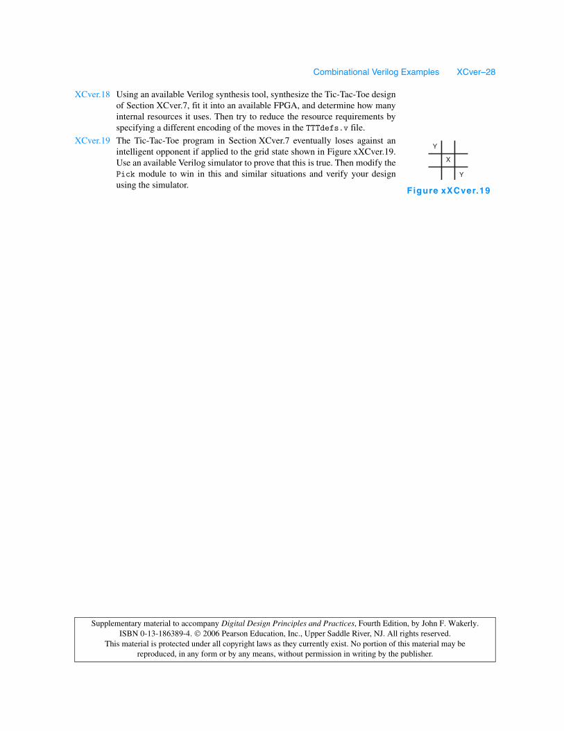
XCver.19 The Tic-Tac-Toe program in Section XCver.7 eventually loses against anintelligent opponent if applied to the grid state shown in Figure xXCver.19.Use an available Verilog simulator to prove that this is true. Then modify thePick module to win in this and similar situations and verify your designusing the simulator.
X
Y
Y
Figure xXCver.19