your name: solutions by prof. guvench your …eelinux.ee.usm.maine.edu/courses/ele342/class notes...
TRANSCRIPT
Your Name: Your Page No.: / _ SOLUTIONS by Prof. Guvench
* HAPPY HOLIDAYS an BEST WISHES FOR THE NEW YEAR !
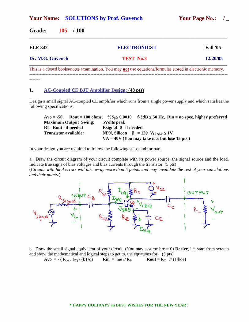
Grade: 105 / 100 ________________________________________________________________________________________ ELE 342 ELECTRONICS I Fall '05 Dr. M.G. Guvench TEST No.3 12/20/05 ________________________________________________________________________________________ This is a closed books/notes examination. You may not use equations/formulas stored in electronic memory. -------------------------------------------------------------------------------------------------------------------------------------------- 1. AC-Coupled CE BJT Amplifier Design: (48 pts) Design a small signal AC-coupled CE amplifier which runs from a single power supply and which satisfies the following specifications. Avo = -50, Rout = 100 ohms, %Sβ≤ 0.0010 f-3dB ≤ 50 Hz, Rin = no spec, higher preferred Maximum Output Swing: 5Volts peak RL=Rout if needed Rsignal=0 if needed Transistor available: NPN, Silicon βF = 120 VCESAT ≤ 1V VA = 40V (You may take it ∞ but lose 15 pts.) In your design you are required to follow the following steps and format: a. Draw the circuit diagram of your circuit complete with its power source, the signal source and the load. Indicate true signs of bias voltages and bias currents through the transistor. (5 pts) (Circuits with fatal errors will take away more than 5 points and may invalidate the rest of your calculations and their points.)
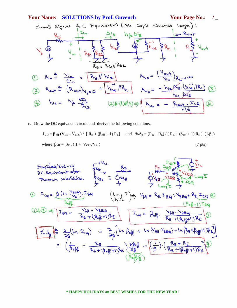
b. Draw the small signal equivalent of your circuit. (You may assume hre = 0) Derive, i.e. start from scratch and show the mathematical and logical steps to get to, the equations for, (5 pts) Avo = - ( Rout . ICQ / (kT/q) Rin = hie // RB Rout = RC // (1/hoe)
Your Name: Your Page No.: / _ SOLUTIONS by Prof. Guvench
* HAPPY HOLIDAYS an BEST WISHES FOR THE NEW YEAR !
c. Draw the DC equivalent circuit and derive the following equations, ICQ = βeff (VBB - VBEQ) / [ RB + (βeff + 1) RE] and %Sβ = (RB + RE) / [ RB + (βeff + 1) RE ] (1/βF) where βeff = βF . ( 1 + VCEQ/VA ) (7 pts)
Your Name: Your Page No.: / _ SOLUTIONS by Prof. Guvench
* HAPPY HOLIDAYS an BEST WISHES FOR THE NEW YEAR !
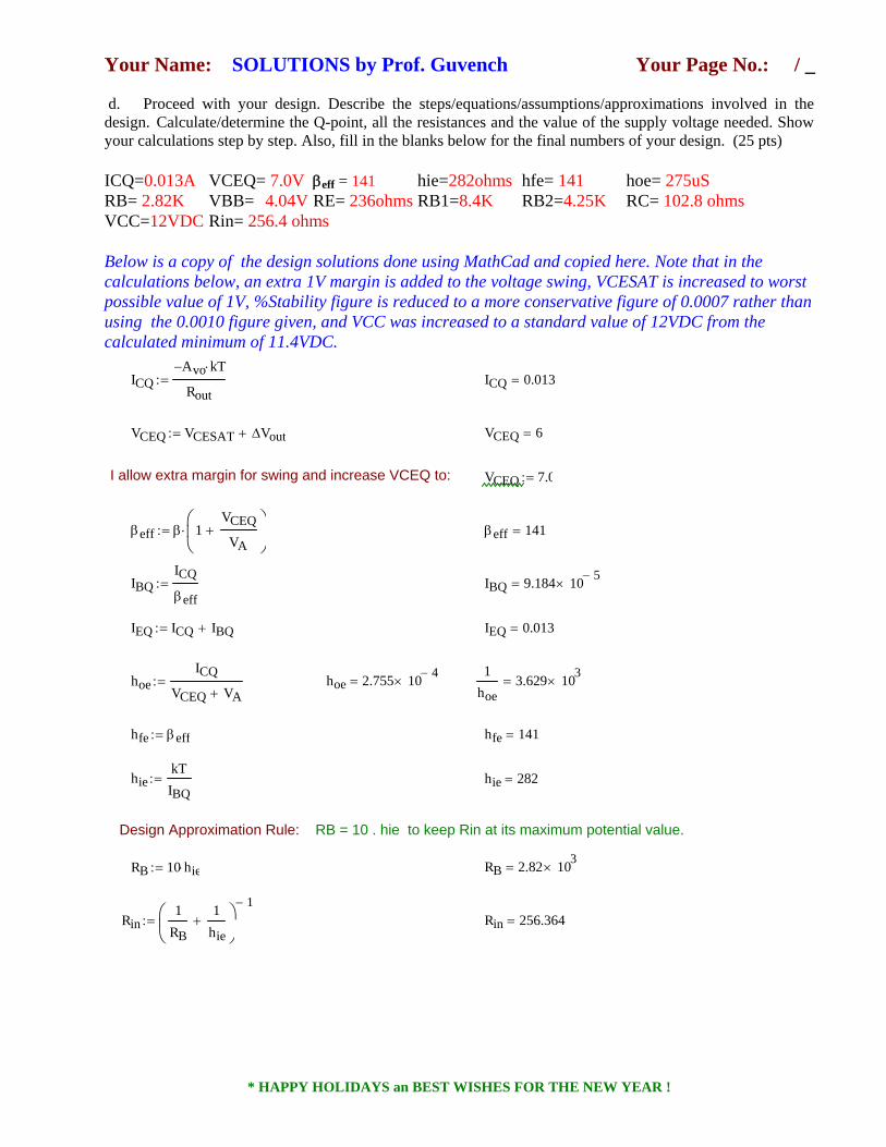
d. Proceed with your design. Describe the steps/equations/assumptions/approximations involved in the design. Calculate/determine the Q-point, all the resistances and the value of the supply voltage needed. Show your calculations step by step. Also, fill in the blanks below for the final numbers of your design. (25 pts) ICQ=0.013A VCEQ= 7.0V βeff = 141 hie=282ohms hfe= 141 hoe= 275uS RB= 2.82K VBB= 4.04V RE= 236ohms RB1=8.4K RB2=4.25K RC= 102.8 ohms VCC=12VDC Rin= 256.4 ohms Below is a copy of the design solutions done using MathCad and copied here. Note that in the calculations below, an extra 1V margin is added to the voltage swing, VCESAT is increased to worst possible value of 1V, %Stability figure is reduced to a more conservative figure of 0.0007 rather than using the 0.0010 figure given, and VCC was increased to a standard value of 12VDC from the calculated minimum of 11.4VDC.
ICQ
Avo− kT⋅
Rout:= ICQ 0.013=
VCEQ VCESAT ∆Vout+:= VCEQ 6=
I allow extra margin for swing and increase VCEQ to: VCEQ 7.0:=
βeff β 1VCEQ
VA+
⎛⎜⎝
⎞
⎠⋅:= βeff 141=
IBQICQ
βeff:= IBQ 9.184 10 5−
×=
IEQ ICQ IBQ+:= IEQ 0.013=
hoeICQ
VCEQ VA+:= 1
hoe3.629 103
×= hoe 2.755 10 4−×=
hfe βeff:= hfe 141=
hiekTIBQ
:= hie 282=
Design Approximation Rule: RB = 10 . hie to keep Rin at its maximum potential value.
RB 2.82 103×= RB 10 hie⋅:=
Rin1
RB
1hie
+⎛⎜⎝
⎞⎠
1−:= Rin 256.364=
Your Name: Your Page No.: / _ SOLUTIONS by Prof. Guvench
* HAPPY HOLIDAYS an BEST WISHES FOR THE NEW YEAR !
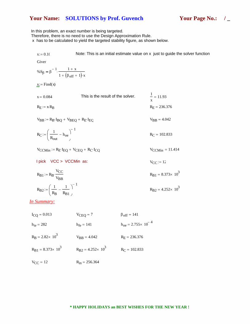
In this problem, an exact number is being targeted.
Therefore, there is no need to use the Design Approximation Rule. x has to be calculated to yield the targeted stability figure, as shown below.
Note: This is an initial estimate value on x just to guide the solver function x 0.10:=
Given
%Sβ β1− 1 x+
1 βeff 1+( ) x⋅+⋅
x Find x( ):=
1x
11.93= This is the result of the solver. x 0.084=
RE x RB⋅:= RE 236.376=
VBB RB IBQ⋅ VBEQ+ RE IEQ⋅+:= VBB 4.042=
RC1
Routhoe−⎛
⎜⎝
⎞⎠
1−:= RC 102.833=
VCCMin RE IEQ⋅ VCEQ+ RC ICQ⋅+:= VCCMin 11.414=
I pick VCC > VCCMin as: VCC 12:=
RB1 RB
VCC
VBB⋅:= RB1 8.373 103×=
RB2
1RB
1RB1
−⎛⎜⎝
⎞⎠
1−:= RB2 4.252 103×=
In Summary:
ICQ 0.013= VCEQ 7= βeff 141=
hoe 2.755 10 4−×= hie 282= hfe 141=
RB 2.82 103×= VBB 4.042= RE 236.376=
RB1 8.373 103×= RB2 4.252 103×= RC 102.833=
VCC 12= Rin 256.364=
Your Name: Your Page No.: / _ SOLUTIONS by Prof. Guvench
* HAPPY HOLIDAYS an BEST WISHES FOR THE NEW YEAR !
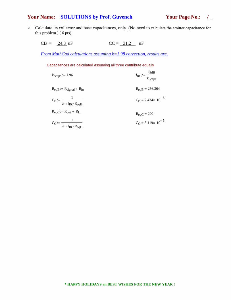
e. Calculate its collector and base capacitances, only. (No need to calculate the emitter capacitance for
this problem.).( 6 pts)
CB = 24.3 uF CC = 31.2 uF From MathCad calculations assuming k=1.98 correction, results are,
Capacitances are calculated assuming all three contribute equally
k3caps 1.96:= fRCf3dB
k3caps:=
ReqB Rsignal Rin+:= ReqB 256.364=
CB1
2 π⋅ fRC⋅ ReqB⋅:= CB 2.434 10 5−
×=
ReqC Rout RL+:= ReqC 200=
CC1
2 π⋅ fRC⋅ ReqC⋅:= CC 3.119 10 5−
×=
Your Name: Your Page No.: / _ SOLUTIONS by Prof. Guvench
* HAPPY HOLIDAYS an BEST WISHES FOR THE NEW YEAR !
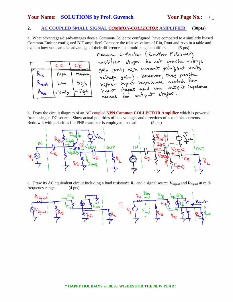
2. AC COUPLED SMALL SIGNAL COMMON-COLLECTOR AMPLIFIER (30pts) a. What advantages/disadvantages does a Common-Collector configured have compared to a similarly biased Common-Emitter configured BJT amplifier? Compare the relative values of Rin, Rout and Avo in a table and explain how you can take advantage of their differences in a multi-stage amplifier. (5 pts)
b. Draw the circuit diagram of an AC coupled NPN Common COLLECTOR Amplifier which is powered from a single DC source. Show actual polarities of bias voltages and directions of actual bias currents. Redraw it with polarities if a PNP transistor is employed, instead. (5 pts)
c. Draw its AC equivalent circuit including a load resistance RL and a signal source VSignal and RSignal at mid-frequency range. (4 pts)
Your Name: Your Page No.: / _ SOLUTIONS by Prof. Guvench
* HAPPY HOLIDAYS an BEST WISHES FOR THE NEW YEAR !
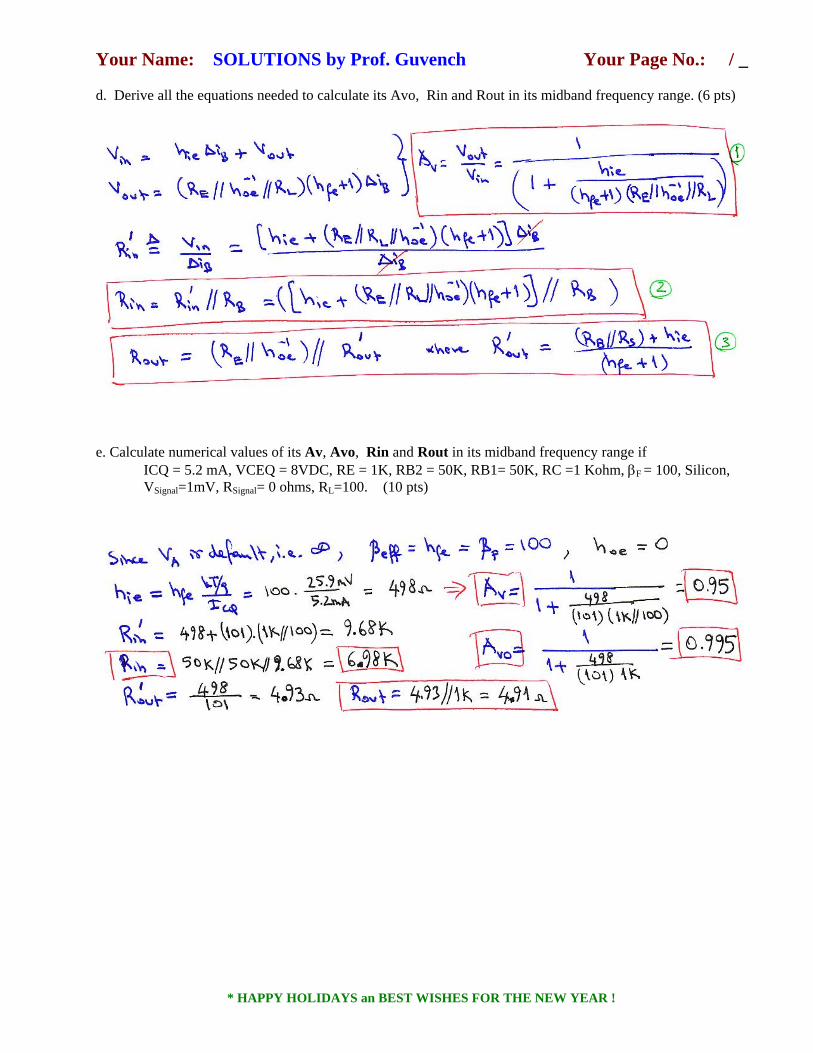
d. Derive all the equations needed to calculate its Avo, Rin and Rout in its midband frequency range. (6 pts)
e. Calculate numerical values of its Av, Avo, Rin and Rout in its midband frequency range if
ICQ = 5.2 mA, VCEQ = 8VDC, RE = 1K, RB2 = 50K, RB1= 50K, RC =1 Kohm, βF = 100, Silicon, VSignal=1mV, RSignal= 0 ohms, RL=100. (10 pts)
Your Name: Your Page No.: / _ SOLUTIONS by Prof. Guvench
* HAPPY HOLIDAYS an BEST WISHES FOR THE NEW YEAR !
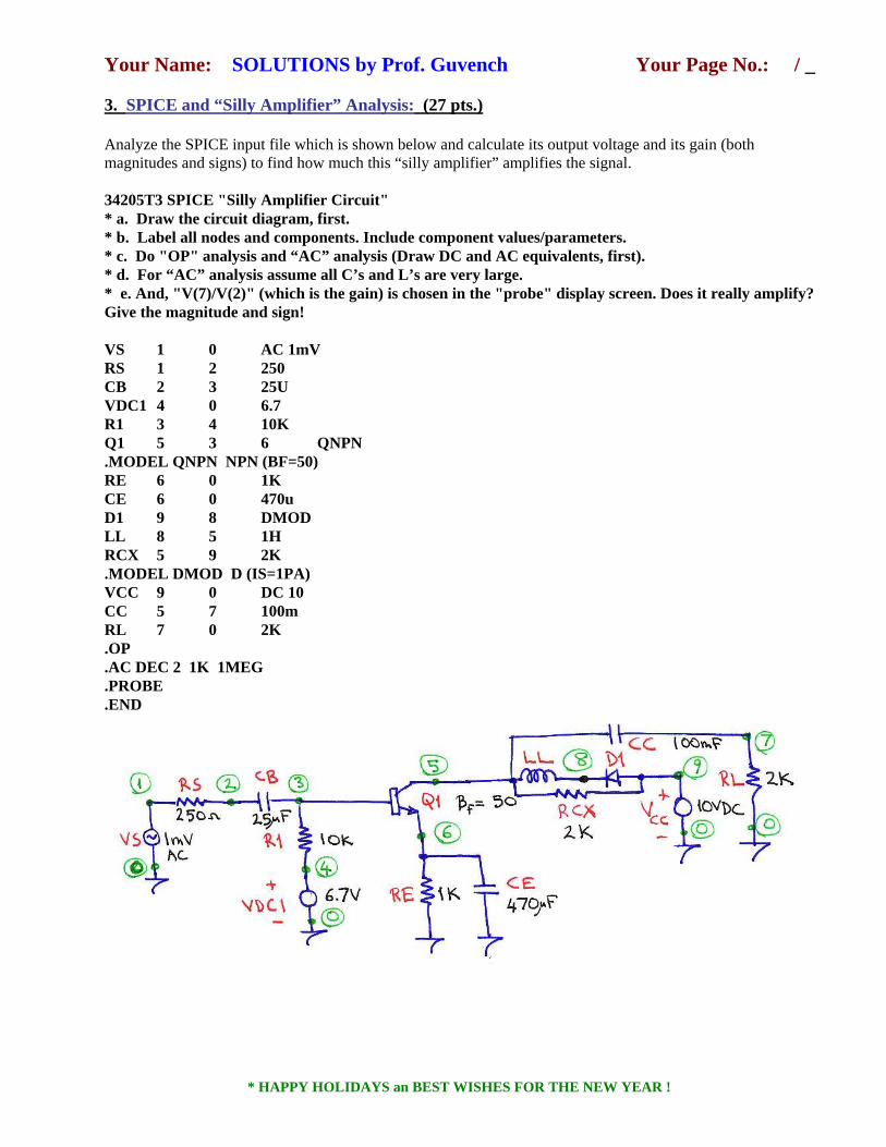
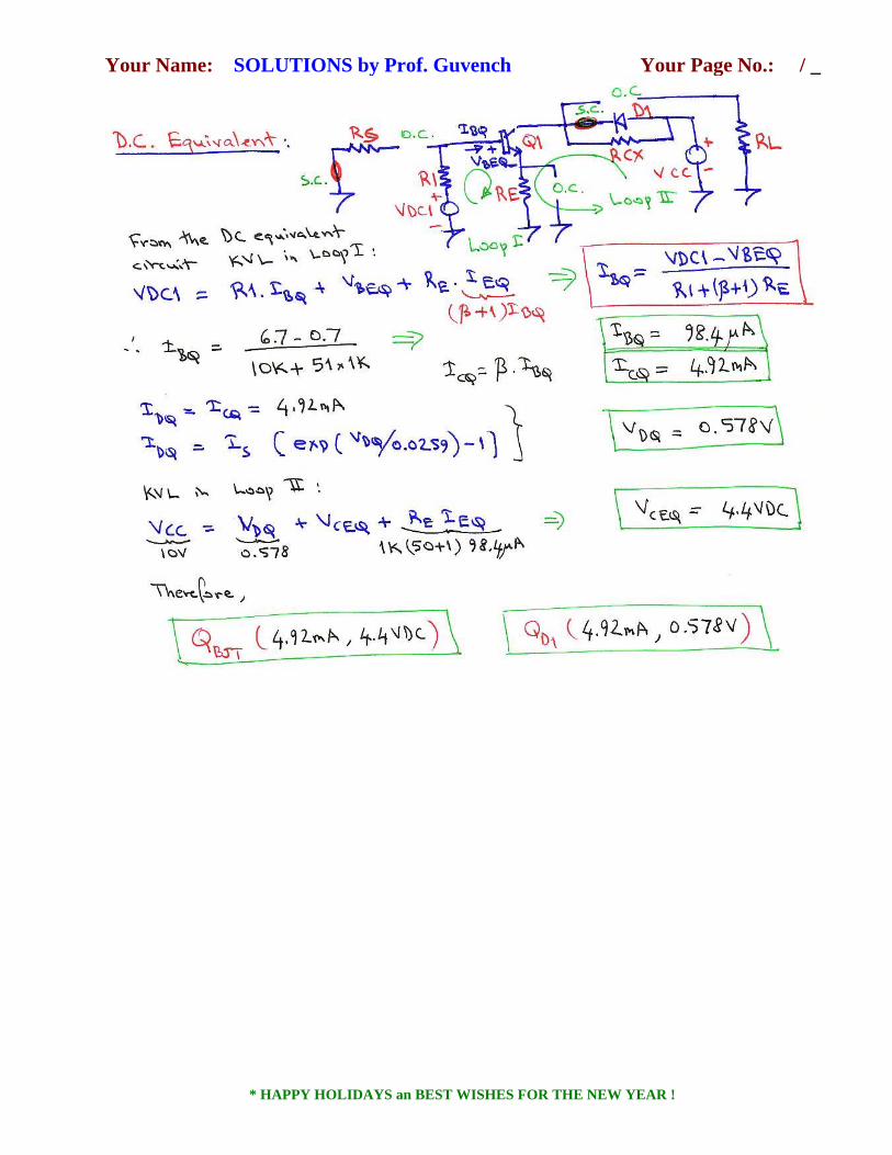
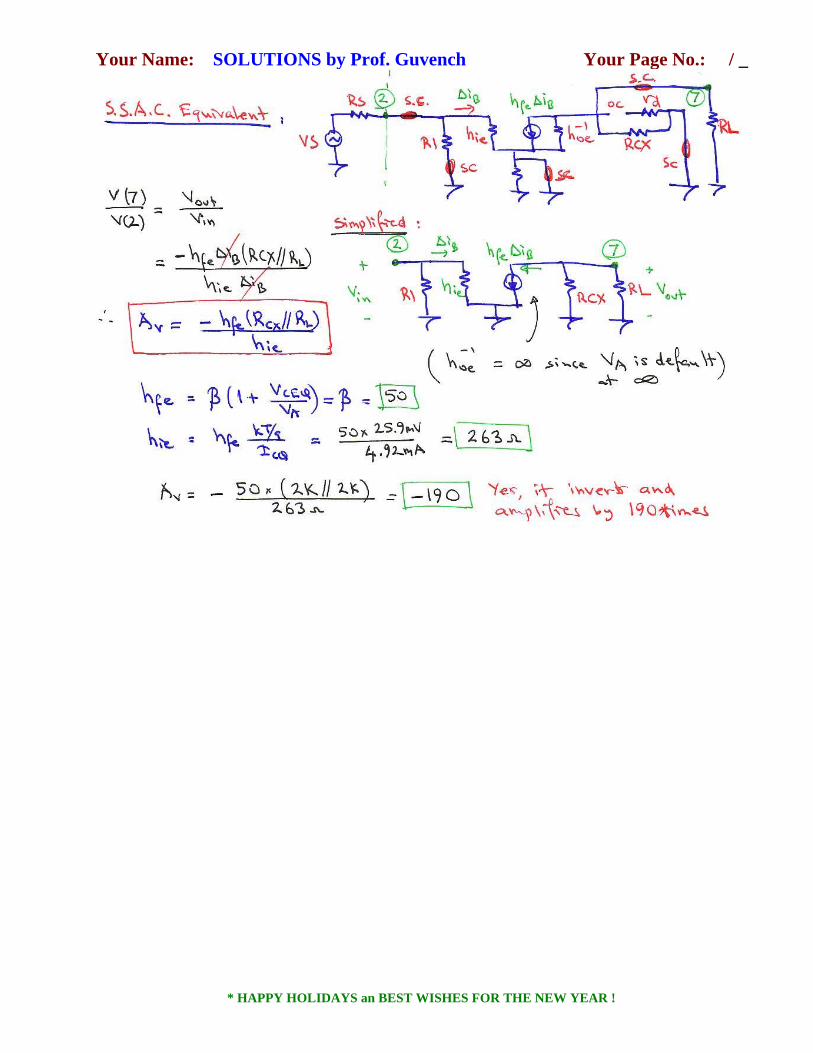
3. SPICE and “Silly Amplifier” Analysis: (27 pts.) Analyze the SPICE input file which is shown below and calculate its output voltage and its gain (both magnitudes and signs) to find how much this “silly amplifier” amplifies the signal. 34205T3 SPICE "Silly Amplifier Circuit" * a. Draw the circuit diagram, first. * b. Label all nodes and components. Include component values/parameters. * c. Do "OP" analysis and “AC” analysis (Draw DC and AC equivalents, first). * d. For “AC” analysis assume all C’s and L’s are very large. * e. And, "V(7)/V(2)" (which is the gain) is chosen in the "probe" display screen. Does it really amplify? Give the magnitude and sign! VS 1 0 AC 1mV RS 1 2 250 CB 2 3 25U VDC1 4 0 6.7 R1 3 4 10K Q1 5 3 6 QNPN .MODEL QNPN NPN (BF=50) RE 6 0 1K CE 6 0 470u D1 9 8 DMOD LL 8 5 1H RCX 5 9 2K .MODEL DMOD D (IS=1PA) VCC 9 0 DC 10 CC 5 7 100m RL 7 0 2K .OP .AC DEC 2 1K 1MEG .PROBE .END
Your Name: Your Page No.: / _ SOLUTIONS by Prof. Guvench
* HAPPY HOLIDAYS an BEST WISHES FOR THE NEW YEAR !
Your Name: Your Page No.: / _ SOLUTIONS by Prof. Guvench
* HAPPY HOLIDAYS an BEST WISHES FOR THE NEW YEAR !