1 st workshop on photocathodes: 20-21 july, 2009, univ. of chicago enhancing electron emission zeke...
Post on 19-Dec-2015
215 views
TRANSCRIPT
1st Workshop on Photocathodes: 20-21 July, 2009, Univ. of Chicago
Enhancing Electron Emission
Zeke Insepov, ANL

2
Outline Introduction – Spicer’s Photoemission model Search for new PC materials
– Band structure of bi- and multi-alkali PC Electron emission enhancement
– Anti-reflecting coatings (Nanorod Arrays, Moth-eye concept)
– Electric field assisted PE MC simulation of pillar photocathode MC simulations of MCP test experiment PC lifetime, aging, ion feedback Summary
3
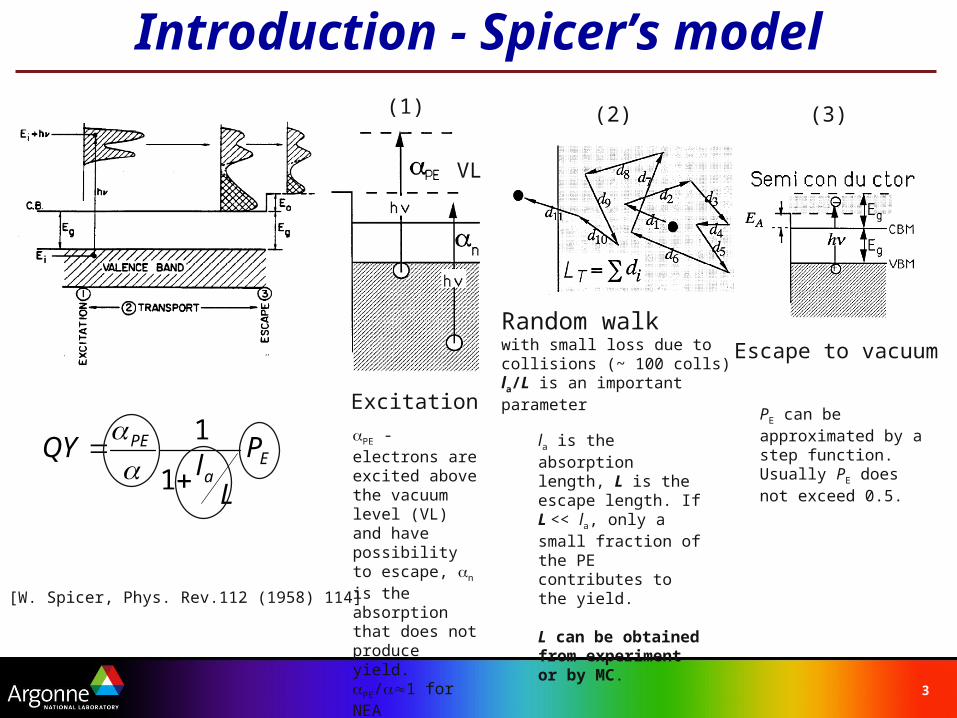
Introduction - Spicer’s model
[W. Spicer, Phys. Rev.112 (1958) 114]
Ea
PE P
Ll
QY
1
1
(3)
PE can be approximated by a step function. Usually PE does not exceed 0.5.
Escape to vacuum
Excitation
(1)
PE - electrons are excited above the vacuum level (VL) and have possibility to escape, n is the absorption that does not produce yield.PE/1 for NEA
VL
(2)
la is the absorption length, L is the escape length. If L << la, only a small fraction of the PE contributes to the yield.
L can be obtained from experiment or by MC.
Random walkwith small loss due to collisions (~ 100 colls)la/L is an important parameter

4
Parameters for efficient PC
The photon absorption la, Ea, Eg : Search for new materials
The diffusion length L:
– In UV region: la/L ~ 104
– For semiconductors: la/L ~ 1
The escape probability PE
– normally it is ~ 0.5
– For CsI : ~ 1
– For metals: < 0.1 Field enhancement, band bending
– (110)-Cs-O: E=0.23eV (GaAs, [2])
– (110): E=0.28eV
– (111A)-Ga: E=0.86eV, w = 155Å, PE=0.21
– (111B)-As: E=0.1eV, w = 51Å, PE=0.49-0.58
NEA[1] Spicer, slac-pub 6306 (1993)[2] James et al, J. Appl. Phys. (1971)
5
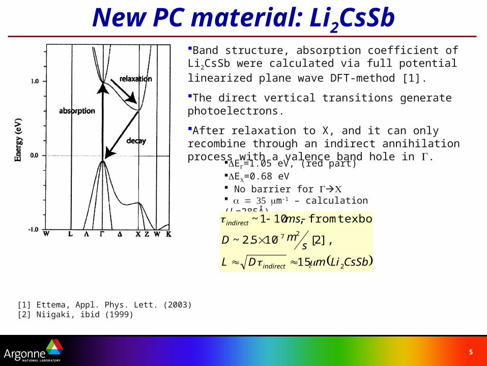
New PC material: Li2CsSbBand structure, absorption coefficient of Li2CsSb were calculated via full potential linearized plane wave DFT-method [1].
The direct vertical transitions generate photoelectrons.
After relaxation to X, and it can only recombine through an indirect annihilation process with a valence band hole in .
[1] Ettema, Appl. Phys. Lett. (2003)[2] Niigaki, ibid (1999)
E=1.05 eV, (red part)E=0.68 eV No barrier for m-1 – calculation (la=285Å)
CsSbLimDL
smD
ms
indirect
indirect
2
27
15
],2[105.2~
texbookfrom,101~

6
Diffusion and drift of carriers
mobility. -
electrons, oflength diffusion the
.1111
1
,111
, timesrelaxation
ion times,recombinat
ts,coefficien band,
ts,coefficiendiffusion -
surface, todistance the
.
,
2
2
2
2
ekTDL
LLLL
LFF
L
PRY
RL
FPY
FF
D
z
zJn
z
nD
zJnn
z
nD
V
X
V
[1] Eden, Mall, Spicer, Phys. Rev. Lett. (1967)[2] James, Moll, Phys. Rev. 183 (1969)
L depends on defects, dislocations, impurities. GaAs – L 1.2-1.6 m for NZn=(1-3)1019 cm-3
Best GaAs PC [doped Ge]: L ~ 5-7 m [1]
Step2: Diffusion
).(
,
,1
,1
,
,
0
2chhe
chch
hh
enii
iihh
iiee
hhhhh
eeeee
NNNe
e
J
e
J
e
JG
GJqt
N
GJqt
N
ENeNeDJ
ENeNeDJ
[Insepov et al, Phys. Rev. A (2008)]
Drift, impact ionization
7
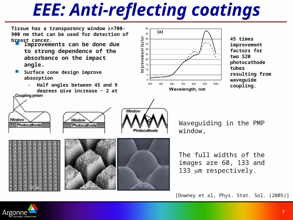
EEE: Anti-reflecting coatings
Improvements can be done due to strong dependence of the absorbance on the impact angle.
Surface cone design improve absorption– Half angles between 45 and 9 degrees
give increase ~ 2 at 400 nm; – 8 times at 850 nm.
[Downey et al, Phys. Stat. Sol. (2005)]
45 times improvement factors for two S20 photocathode tubes resulting from waveguide coupling.
Tissue has a transparency window =700-900 nm that can be used for detection of breast cancer.
Waveguiding in the PMP window,
The full widths of the images are 60, 133 and 133 m respectively.
8
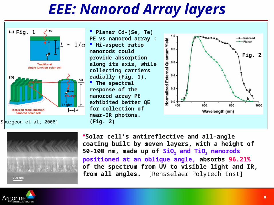
EEE: Nanorod Array layers
[Spurgeon et al, 2008]
Solar cell’s antireflective and all-angle coating built by sseven layers, with a height of 50-100 nm, made up of SiO2 and TiO2 nanorods positioned at an oblique angle, absorbs 96.21% of the spectrum from UV to visible light and IR, from all angles. [Rensselaer Polytech Inst]
Planar Cd-(Se, Te) PE vs nanorod array : Hi-aspect ratio nanorods could provide absorption along its axis, while collecting carriers radially (Fig. 1). The spectral response of the nanorod array PE exhibited better QE for collection of near-IR photons. (Fig. 2)
L ~ 1/
Fig. 1
Fig. 2
Light
charge

9
EEE: Moth-eye concept
The surface of the moth eyes consists of an array of protuberances, termed corneal nipples. The nipples are arranged in domains with hexagonal packing, the distances are from 180 to 240 nm, the nipple heights varied between 0 and 230 nm. The nipples create an interface with a gradient refractive index between that of air and the lens material. The reflectance progressively diminished with increased nipple height. Nipples with a paraboloid shape and height 250 nm, touching each other at the base, virtually completely reduced the reflectance for normally incident light.
[Stavenga et al, Proc. R. Soc. B (2006)]
10
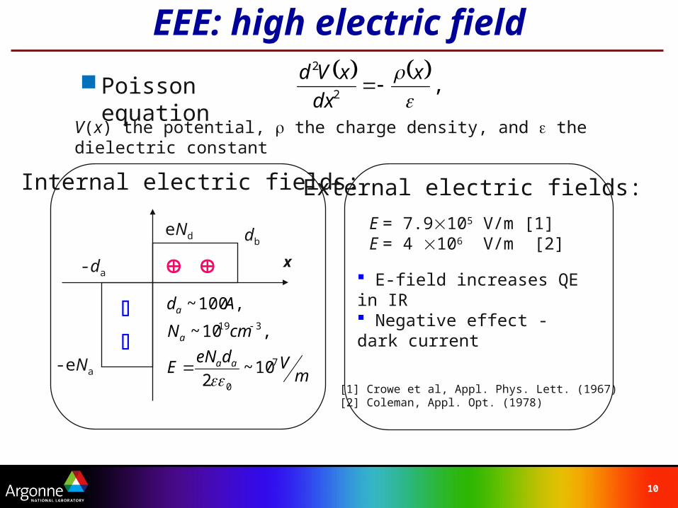
EEE: high electric field
Poisson equation
,2
2
x
dx
xVd
V(x) the potential, the charge density, and the dielectric constant
-da
dbeNd
-eNa
mVdeN
E
cmN
Ad
aa
a
a
7
0
319
10~2
,10~
,100~
Internal electric fields:
x
External electric fields:
E = 7.9105 V/m [1]E = 4 106 V/m [2]
[1] Crowe et al, Appl. Phys. Lett. (1967)[2] Coleman, Appl. Opt. (1978)
E-field increases QE in IR Negative effect - dark current

11
Field Enhancement: Si, GaAs Electric field enhancement from NEA Si, GaAs was observed. E increases the PE and does not change the spectral response of the NEA
surface. Surface potential lowering by the Schottky effect.
[Howorth et al, Appl. Phys. Lett. 1973]
barrierSchottky the
,)(exp
,4 210
B
kTBP
eE
External field E reduces the workfunction via Schottky equation:
w=200Å Si : 51018 cm-3, 0.6 MV/mw=240Å GaAs : 71017 cm-3
Band bending region:
12
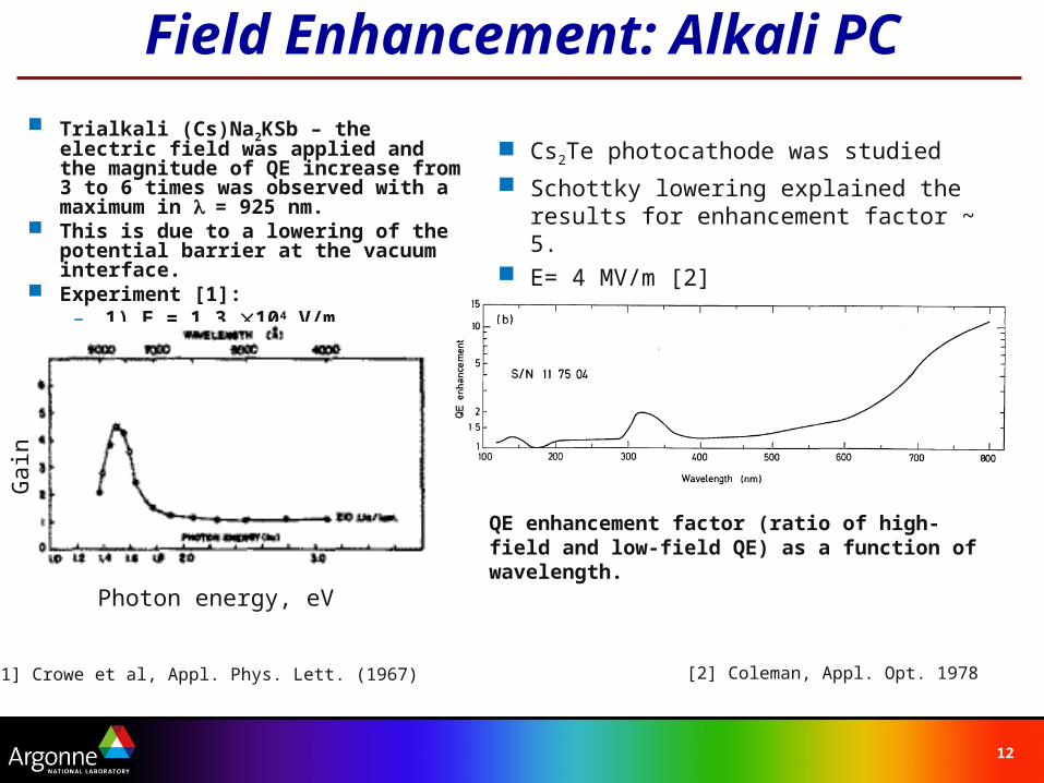
Field Enhancement: Alkali PC
Trialkali (Cs)Na2KSb – the electric field was applied and the magnitude of QE increase from 3 to 6 times was observed with a maximum in = 925 nm.
This is due to a lowering of the potential barrier at the vacuum interface.
Experiment [1]:– 1) E = 1.3 104 V/m– 2) E = 7.9105 V/m
[2] Coleman, Appl. Opt. 1978
Cs2Te photocathode was studied
Schottky lowering explained the results for enhancement factor ~ 5.
E= 4 MV/m [2]
QE enhancement factor (ratio of high-field and low-field QE) as a function of wavelength.
Photon energy, eV
Gai
n
[1] Crowe et al, Appl. Phys. Lett. (1967)
13
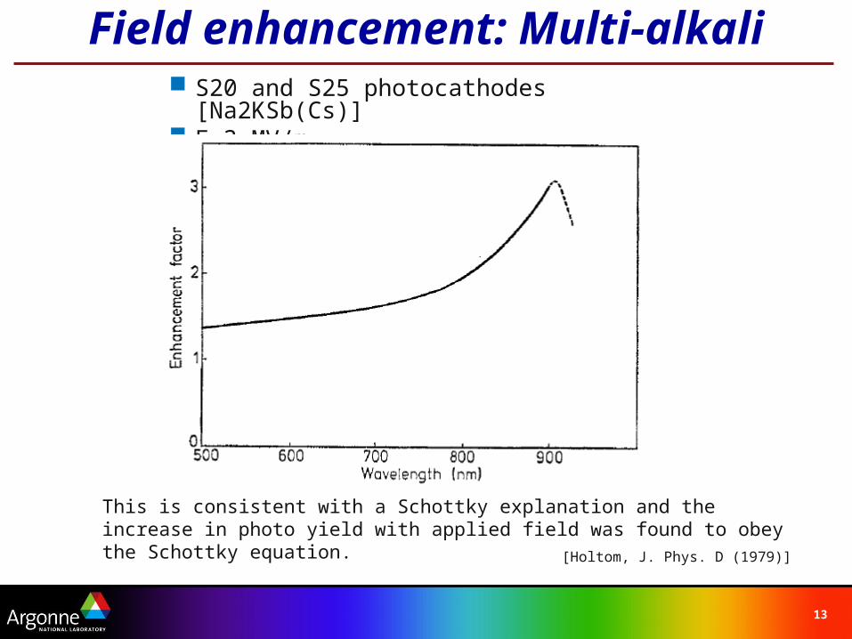
Field enhancement: Multi-alkali S20 and S25 photocathodes [Na2KSb(Cs)] E=3 MV/m
[Holtom, J. Phys. D (1979)]
This is consistent with a Schottky explanation and the increase in photo yield with applied field was found to obey the Schottky equation.

14
MC study - Motivation
Nanostructured PC surface study – MC can recreate roughness, poly- or nano-crystalline, pillar, nipple, or other metamaterial types
Arbitrary doping, impurity and electric field simulation
Arbitrary barrier shapes and realistic escape probability
Testing various electron scattering models
All materials (metals, alkaline, semiconductors)

15
Transport of hot electrons in metals Monte Carlo method was applied to the
problem of “hot” electron motion in metals;
e-e scattering length, e-ph length and attenuation length was obtained.
Specular and diffuse reflectance at the boundaries were simulated.
Comparison with the theory for Au, Ag, Pd.
[Stuart, Wooten, Spicer, Phys.Rev.1964]
LxexP ~
By calculating the number of hot electrons crossing the barrier, for different sample thickness, the attenuation length L can be obtained.
Probability of e- excited at x reach the barrier with E

16
Physical model and parameters
(1) Photoexcitation of carriers – I(x)=I0 exp(-x)
– exponential law with =7.7105 cm-1 (typical for Au) – can be adjusted for different materials;
– Electrons are isotropically distributed in all directions (2) Scattering of excited carriers;
– e-e, e-ph scattering Eph k(- Debye temperature)
– e-impurity/defect scattering (Brooks-Herring law) (3) Escape of carriers over the barrier.
– Elastic scattering interface (no energy change)– Lambert law in direction
[Stuart, Wooten, Spicer, Phys.Rev.1964]

17
Algorithm of MC program Initial source of electrons S(X,E) is created
– E = EF + h-(h-e)c1, 0c11
– Exp attenuation: X=T+(1/)ln{1-c2[1-exp (-T)},
• T – sample thickness, 0c21
– Collision simulation: lT=lelp/(le+lp) – the mean free path
– Exp law: l=lT |ln c3|, 0c31
– Angle to normal: cos = 2c4 -1, 0c41 (all d are eq. probable)
– c5 < lT/le, 0c51 – choice for kind of collision
New electron, new trajectory, similar to previous
– The process continued until the electron E < E0
10,000 trajectories computed for each sample; (statistics) 200, 400, 600, 800 , and 1000Å samples were simulated Specular reflection from the vacuum boundary[Stuart, Wooten, Spicer, Phys.Rev.1964]
18
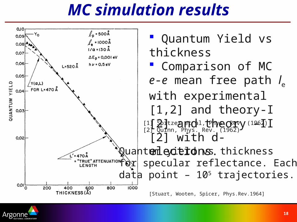
MC simulation results
[Stuart, Wooten, Spicer, Phys.Rev.1964]
Quantum Yield vs thickness Comparison of MC e-e mean free path le with experimental [1,2] and theory-I [2] and theory –II [2] with d-electrons.
[1] Spitzer et al, Phys. Rev. (1962)[2] Quinn, Phys. Rev. (1962)
Quantum yield vs thicknessfor specular reflectance. Each data point – 105 trajectories.

19
Pillar structure
Glass window
photon
Secondary electrons

20
Pillar simulation
TiO2TiO2
TiO2 pillar ( ~ 50-200 nm)
Absorber (Al or GaAs), d ~ 50 nm
Low work-function coating (CsO), d ~ 10 nm
Cross-section of pillar
TiO2pillar
CsO photocathode
Al absorber CsO, d ~ 10 nm
E=2-5 V/mPhoton secondary
electron
Z. Insepov, V. Ivanov
Absorber (Al or GaAs), d ~ 50 nm
primary electron
21
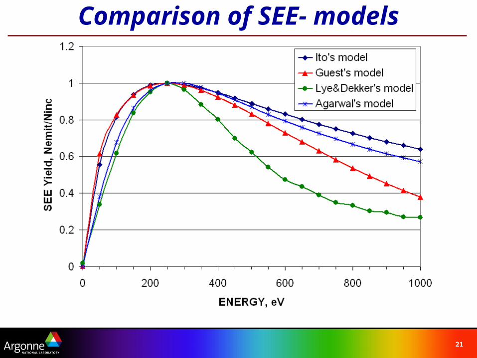
Comparison of SEE- models

22
PC simulation parameters
Photon energy : 1.5-6.2 eV (800nm-200nm) 1.4eV
Kinetic energy of SEE: 0.5-5 eVElectric field ~ 2-5 V/µm accelerates PE to 2.5-
10 eVElectric field geometry is being determined by
the resistivity of PC: 100 MComsol

23
Pillar Simulation Geometry
Z. Insepov, V. Ivanov
24
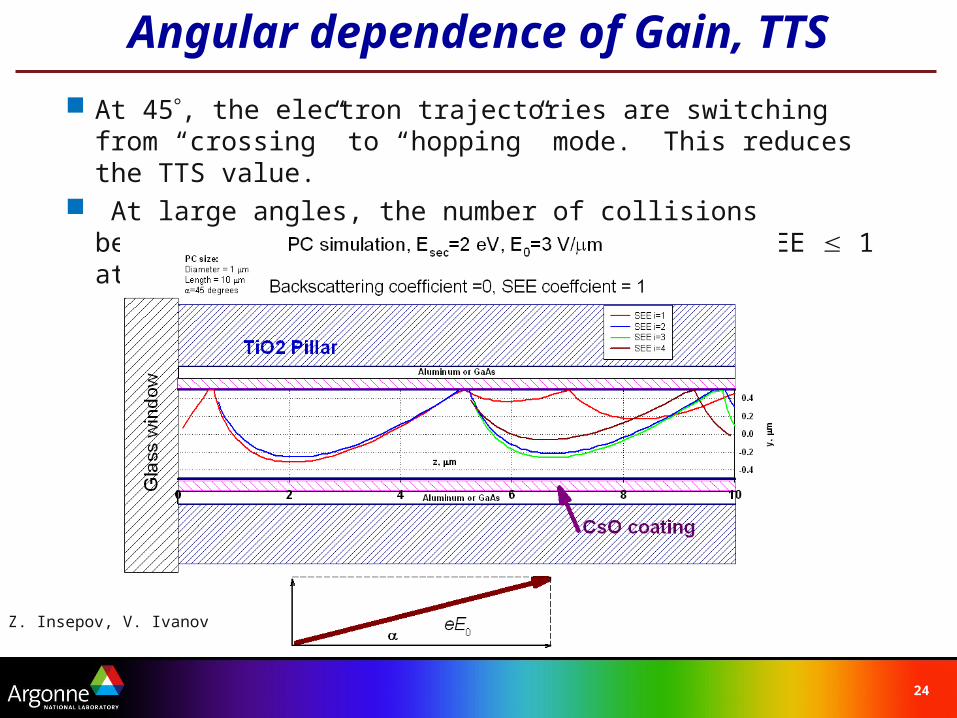
Angular dependence of Gain, TTS
At 45, the electron trajectories are switching from “crossing” to “hopping” mode. This reduces the TTS value.
At large angles, the number of collisions becomes higher and that reduces the Gain: SEE 1 at small energies.
Z. Insepov, V. Ivanov

25
TTS for normal and inclined pillars

26
Gain and TTS vs pillar angle
Switching to hopping mode

27
Time drift simulation for APS setup
dCsI=120 nm
[Experiment: M. Wetstein (ANL)]

28
APS experiments
[Experiment: M. Wetstein (ANL)]
29
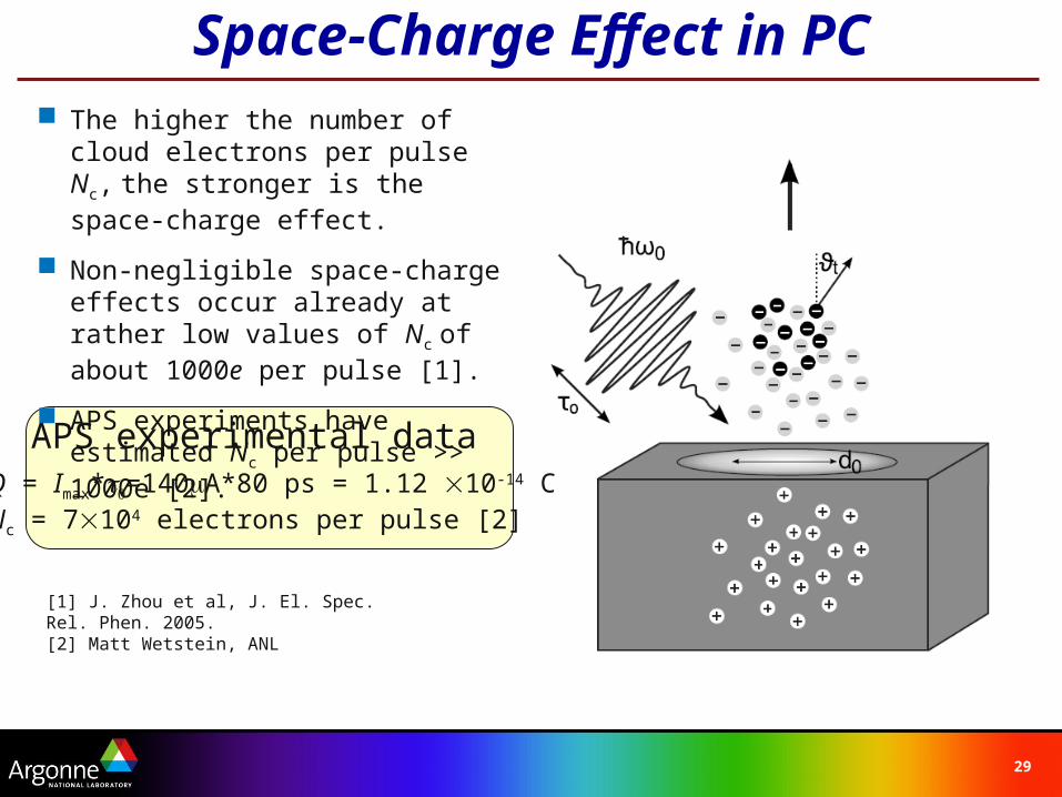
Space-Charge Effect in PC The higher the number of cloud
electrons per pulse Nc, the stronger is the space-charge effect.
Non-negligible space-charge effects occur already at rather low values of Nc of about 1000e per pulse [1].
APS experiments have estimated Nc per pulse >> 1000e [2].
[1] J. Zhou et al, J. El. Spec. Rel. Phen. 2005.[2] Matt Wetstein, ANL
Q = Imax*=140A*80 ps = 1.12 10-14 CNc = 7104 electrons per pulse [2]
APS experimental data

30
Drift-diffusion model of electrons
hEg
e-Escape length in CsILnm[1]
<v> E = U/d
Drift+Diffusion modelLaser beam
Vacuum [2] /108
mobility,
),(2)()(
,0)(
force, random
t,coefficienfriction
field, electric)(
,/)(/)()(
24e
ee
sVm
me
ttm
TktRtR
tR
R
rUE
mRtvmrUtv
e
e
B
i
i
eiieii
Langevin equation
[1] Breskin, NIMA (1996)[2] Aduev, Phys. Stat. Sol. B (1998) [3] Boutboul, J. Appl. Phys. (1998)
Absorption length in CsI at =220 nm
lanm[3]

31
MC model of random walk
E
,)-(1
5.31
,]2[ 16~
y,diffusivitelectron ,
,03.0/1
[1],length absorption ,221
QERY
keVU
nmL
DL
nmL
nmL
D
eD
a
window
vacu
um
z
La
Ld
Ld – e-e + e-ph + e-defects
e
Photocathode
CsI
[1] Boutboul, J. Appl. Phys. (1998)[2] Breskin, NIMA (1996)

32
Random walk + drift
E
Ld=10 nmLa=100 nmthick=120 nmm*=0.1mU=1-3.5 keV
33
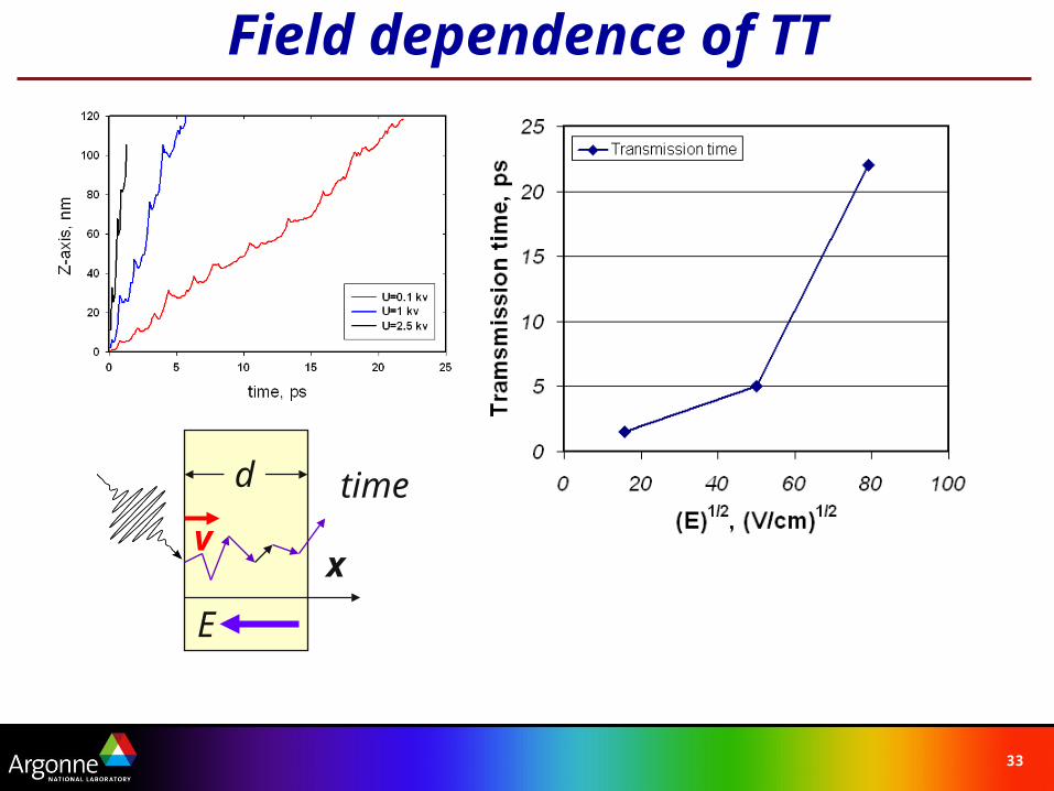
Field dependence of TT
xv
d
E
time

34
Time to Drift in vacuum
35
Summary Electron emission can be enhanced by various
methods: nanostructured interfaces, doping and applying electric fields, multilayer coatings, NEA
Theory and simulation methods are not yet capable of treating complex PC tasks, such as surface roughness, nano-structured, real material properties, hot carriers and plasma effects, high electric fields in PC, aging
Nano-pillar PC structure was simulated and optimized
MC method is being developed to evaluate surface roughness, plasma and hot electrons effects, complex materials, high electric fields and photon fluxes.

36
Acknowledgments
H. Frisch, ANL V. Ivanov, Muon Inc. K. Attenkofer, ANL A. Terekhov, Novosibirsk, Russia