1 the physical structure (nmos) field oxide sio2 gate oxide field oxide n+ al sio2 polysilicon gate...
TRANSCRIPT
1CONCORDIAVLSI DESIGN LAB
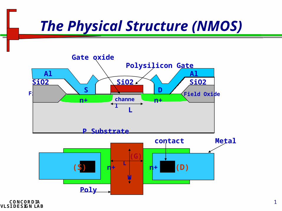
The Physical Structure (NMOS)
Field Oxide
SiO2
Gate oxide
Field Oxiden+n+
AlAlSiO2SiO2
Polysilicon Gate
channel
L
P Substrate
D S
L
W
(D) (S)
Metal
n+ n+
(G)
Poly
contact
2CONCORDIAVLSI DESIGN LAB
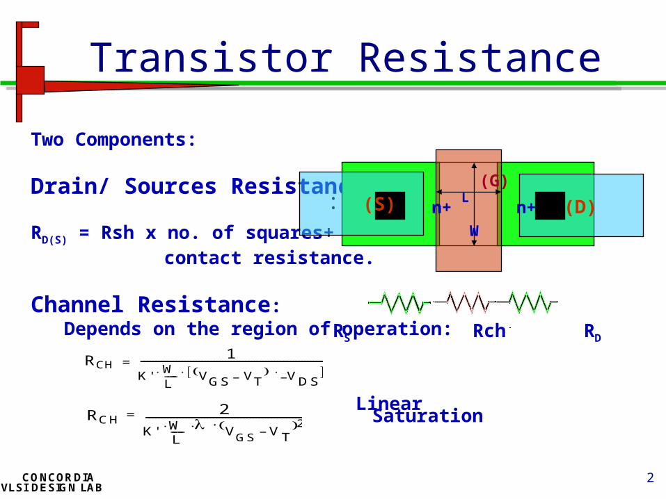
Transistor Resistance
:
Two Components:
Drain/ Sources Resistance:
RD(S) = Rsh x no. of squares+ contact resistance.
Channel Resistance: Depends on the region of operation:
L
W
(D) (S) n+ n+
(G)
RS Rch RD
Linear
RCH2
K' WL----- V
GSVT– 2
----------------------------------------------------= Saturation
RCH1
K'WL----- VGS VT– VDS–
---------------------------------------------------------------- '=

3CONCORDIAVLSI DESIGN LAB
Transistor Geometry

4CONCORDIAVLSI DESIGN LAB
Transistor Geometry- Detailed

5CONCORDIAVLSI DESIGN LAB
NMOS Operation-Linear
K Cox= Process Transconductance uA/V2
for 0.35u, K’ (Kp)=196uA/ V2
Cox
ox
tox-------= Gate oxide capacitance per unit area
ox = 3.9 x o = 3.45 x 10⁻¹¹ F/m
tox Oxide thickness
for 0.35 , tox=100Ao
Quick calculation of Cox: Cox= 0.345/tox (Ao) pf/um2
= mobility of electrons 550 cm2/V-sec for 0.35 process
VDS
IDS
VGS
IDS N KN VG SN VTN– VD SN12---VD SN
2–
= KN=K’.
W/L

6CONCORDIAVLSI DESIGN LAB
NMOS Operation-Linear
Effect of W/L
Effect of temperature
RdsW/L
W
temp Rds
W

7CONCORDIAVLSI DESIGN LAB
Variations in Width and Length
Weff
Wdrawn
WD WD
1. Width Oxide encroachment Weff= Wdrawn-2WD
2. Length Lateral diffusion LD = 0.7Xj Leff= Ldrawn-2LD
Ldrawn
LD Leff LD
polysilicon
polysilicon
8CONCORDIAVLSI DESIGN LAB
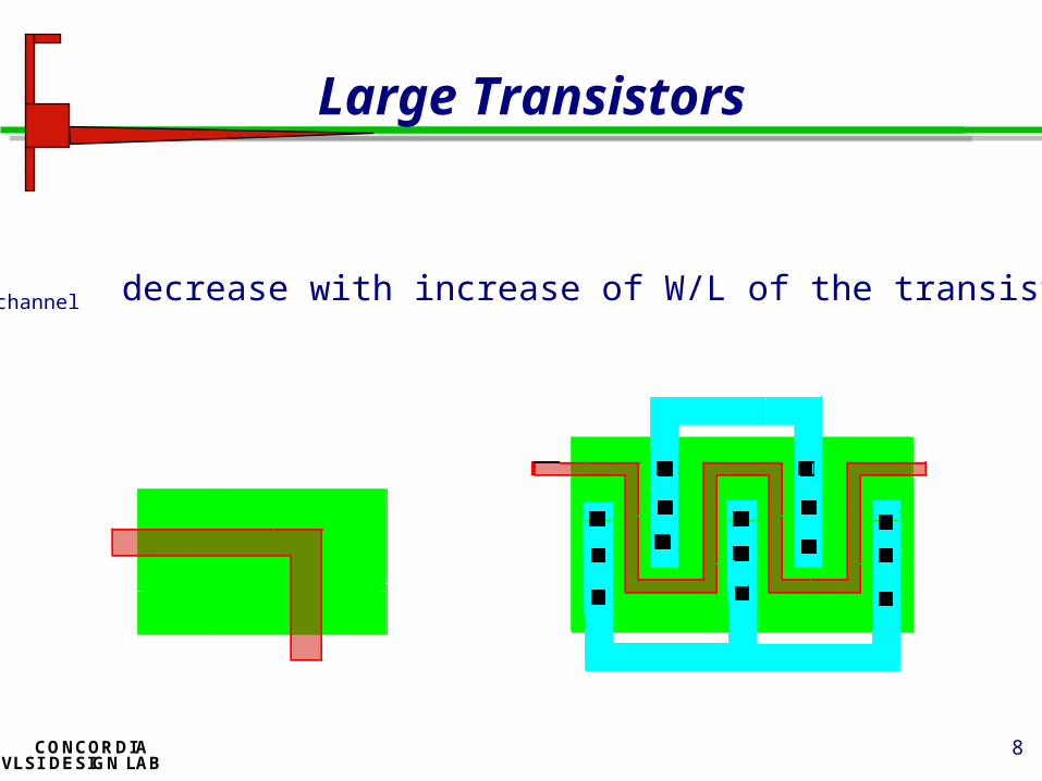
Large Transistors
Rchannel decrease with increase of W/L of the transistor

9CONCORDIAVLSI DESIGN LAB
Semiconductor Resistors
Resistance
R= p(l /A) = (p/t). (l /w) = Rsh. (l /w)
Rsh = Sheet resistance /
For 0.5u process: N+ diffusion : 70 / M1: 0.06 P+ diffusion : 140 / M2: 0.06 Polysilicon : 12 / M3: 0.03 Polycide:2-3 / P-well: 2.5K N-well: 1K
w
current
l t
(A)
1
n n q p p q + ------------------------------------------------=

10CONCORDIAVLSI DESIGN LAB
Semiconductor Resistors
AlAl
n+
Diffusionn+
Field oxide
polysilicon
Polysilicon Resistor Diffusion Resistor
SiO2

11CONCORDIAVLSI DESIGN LAB
Semiconductor Capacitors
1. Poly Capacitor: a. Poly to substrate b. Poly1 to Poly2
2. Diffusion Capacitor
n+ (ND)
depletion region
substrate (NA)bottomwallcapacitance
sidewallcapacitances
12CONCORDIAVLSI DESIGN LAB
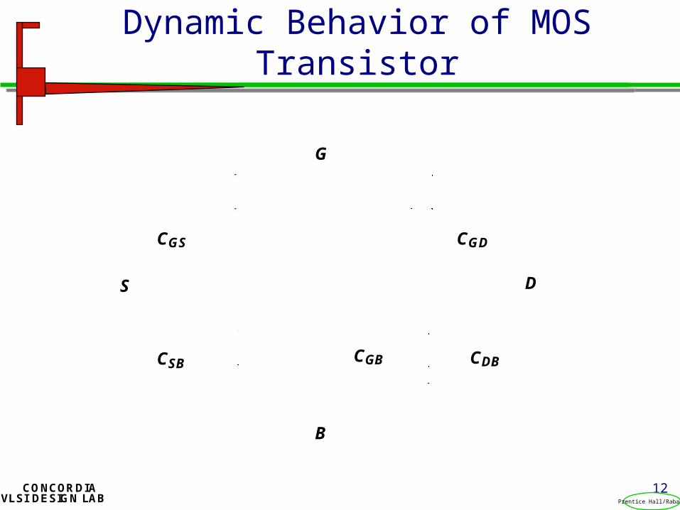
Dynamic Behavior of MOS Transistor
DS
G
B
CGDCGS
CSB CDBCGB
Prentice Hall/Rabaey

13CONCORDIAVLSI DESIGN LAB
SPICE Parameters for Parasitics
Prentice Hall/Rabaey

14CONCORDIAVLSI DESIGN LAB
SPICE Transistors Parameters
Prentice Hall/Rabaey

15CONCORDIAVLSI DESIGN LAB
Modelling: Resistance
1. Resistance: Rint= Rsh [l/w]
Rsh values for 0.35u CMOS Process: Polysilicon 10 / Polycide 2 / Metal1 0.07 / Metal II 0.07 / Metal III 0.05 /
Contact resistance: PolyI to MetalI 50 Via resistance: Metal I to Metal II 1.5 Via resistance: Metal II to metal III 1.

16CONCORDIAVLSI DESIGN LAB
CMOS Inverter: Steady State Response
VDD VDD
VoutVout
Vin = VDD Vin = 0
Ron
Ron
VOH = VDD
VOL= 0

17CONCORDIAVLSI DESIGN LAB
Switching Characteristics of Inverters
VDD
Vout
Vin = VDD
Ron
CL
tpHL = f(Ron.CL)
= 0.69 RonCL
t
Vout
VDD
RonCL
1
0.5
ln(0.5)
0.36
Transient Response
18CONCORDIAVLSI DESIGN LAB
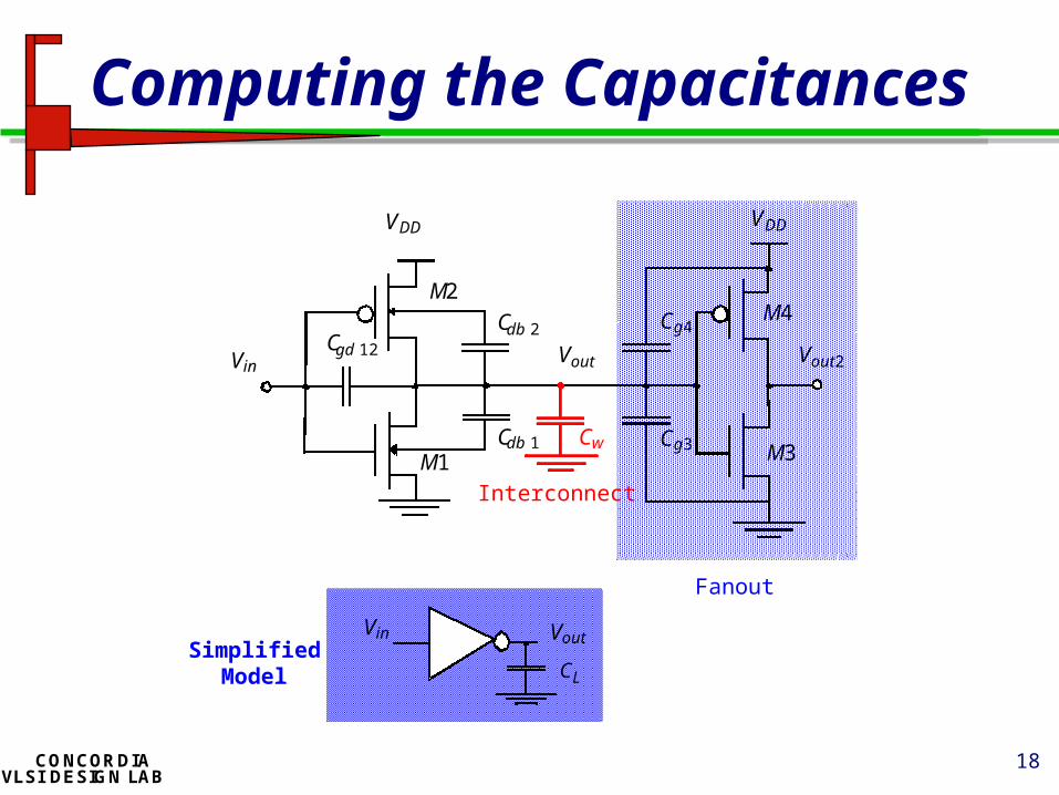
Computing the Capacitances
VDD VDD
Vin Vout
M1
M2
M3
M4Cdb 2
Cdb 1
Cgd 12
Cw
Cg4
Cg3
Vout2
Fanout
Interconnect
VoutVin
CLSimplified
Model

19CONCORDIAVLSI DESIGN LAB
Computing the Capacitances

20CONCORDIAVLSI DESIGN LAB
Delay Definitions
tpHL
tpLH
t
t
Vin
Vout
50%
50%
tr
10%
90%
tf

21CONCORDIAVLSI DESIGN LAB
Step Response
Fall Delay Time: TPHL
Vin
IDN Vin = 5
Vin = 4
Vin = 3
VDD=5V
Vin
G
S
D
D
G
S
Vo
GND
MP
MN
CL
VDD
VDDVoVDD-VT
MN OFF Saturation Linear
(VDSAT)

22CONCORDIAVLSI DESIGN LAB
Step Response- Fall time, tf
trCL
KPVDD 1 p+( )--------------------------------------- 2–( ) 1 p+( )
1 p+( )---------------------------- 19 20p+( )ln+=
DDn
L
V
Ck
.
.
DDp
L
V
Ck
.
.
vin
vo1-n
td1 td2
1
0.1
0.9
tfCL
KNVDD 1 n–( )--------------------------------------- 2 n 0.1–( )
1 n–( )------------------------ 19 20n–( )ln+=
tf=~ k is a constant
tr=~ k is a constant
0.1
23CONCORDIAVLSI DESIGN LAB
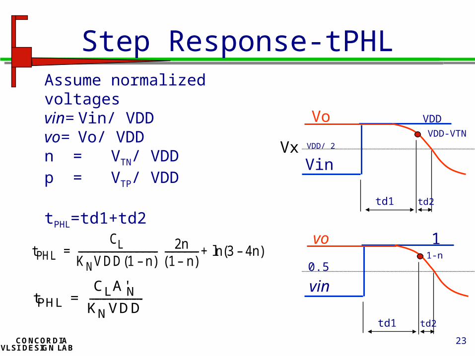
Step Response-tPHL
Vin
VoVDD-VTN
Vx
td1 td2
vin
vo1-n
td1 td2
VDD
1
0.5
VDD/ 2
Assume normalized voltagesvin= Vin/ VDDvo= Vo/ VDDn = VTN/ VDDp = VTP/ VDD
tPHL=td1+td2
tPHLCL
KNVDD 1 n–( )--------------------------------------- 2n
1 n–( )---------------- 3 4n–( )ln+=
tPHLCLA'N
KNVDD----------------------=

24CONCORDIAVLSI DESIGN LAB
Step Response Rise Delay tPLH and Rise Time tr
VDD
Vin
G
S
D
D
G
S
Vo
GND
MP
MN
CL
VDD
tPLHCL
KPVDD 1 p+( )--------------------------------------- 2p–
1 p+( )----------------- 3 4p+( )ln+=
tPLHCLA'P
KPVDD---------------------=
trCL
KPVDD 1 p+( )--------------------------------------- 2–( ) 1 p+( )
1 p+( )---------------------------- 19 20p+( )ln+=
tr4C LA'PKPVDD---------------------= (P= - 0.2)
0.1
25CONCORDIAVLSI DESIGN LAB
Factors Influence Delay
Inverter Delay,td = (tPHL+tPLH)/2
The following factors influence the delay of the inverter:
• Load Capacitance• Supply Voltage• Transistor Sizes• Junction Temperature• Input Transition Time
26CONCORDIAVLSI DESIGN LAB
Delay as a function of VDD
0
4
8
12
16
20
24
28
2.00 4.001.00 5.003.00
Nor
mal
ized
Del
ay
VDD (V)
27CONCORDIAVLSI DESIGN LAB
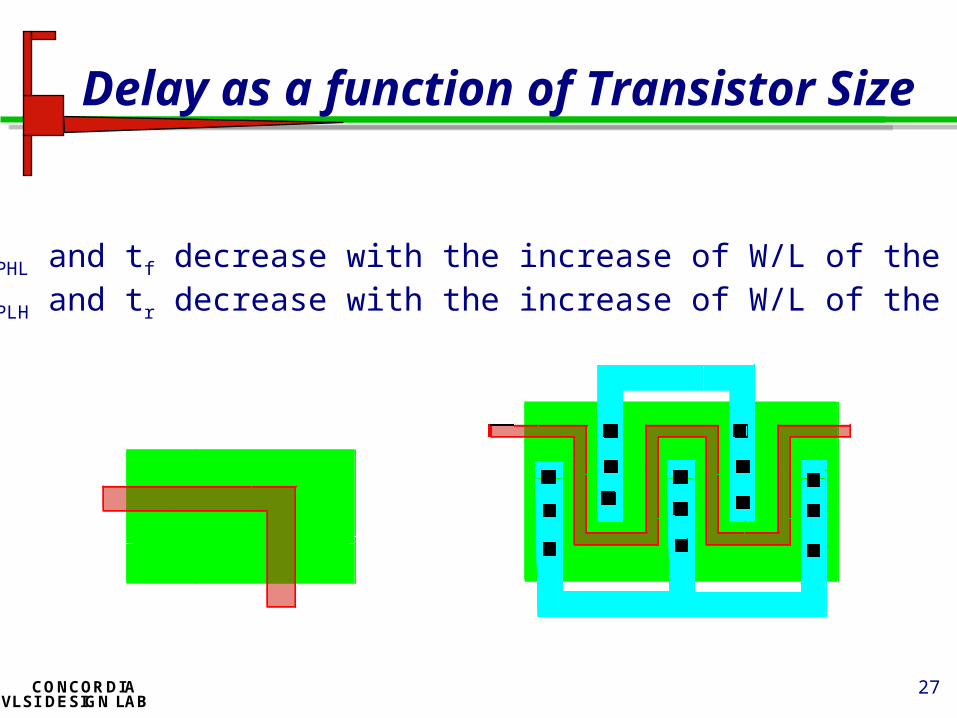
Delay as a function of Transistor Size
tPHL and tf decrease with the increase of W/L of the NMOS tPLH and tr decrease with the increase of W/L of the PMOS

28CONCORDIAVLSI DESIGN LAB
Temperature Effect
Temperature ranges: commercial : 0 to700C industrial: -40 to 850C military: -55 to 1250C Calculation of the junction temperature tj= ta + ja X Pd Effect of temperature on mobility Delay and speed implications

29CONCORDIAVLSI DESIGN LAB
Effect of Input Transition Times
rVinVo
The delay of the inverter increaseswith the increase of the input transition times r and f
tPHL = (tPHL) step + (r /6).(1-2p)
tPLH = (tPLH) step + (f/6).(1+2n)

30CONCORDIAVLSI DESIGN LAB
Define = (W/L)p/(W/L)n
For Equal Fall and Rise Delay KN=KP
= n/ p
For Minimum Delay dtD/d = 0
opt = Sqrt (n/ p)
Transistor Sizing
31CONCORDIAVLSI DESIGN LAB
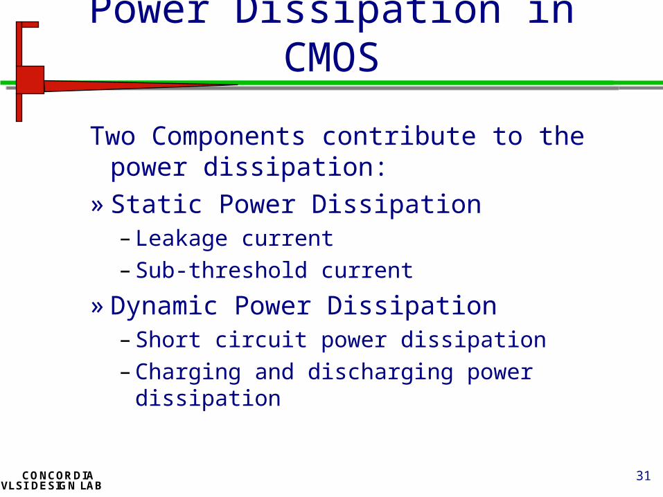
Power Dissipation in CMOS
Two Components contribute to the power dissipation:
» Static Power Dissipation– Leakage current– Sub-threshold current
» Dynamic Power Dissipation– Short circuit power dissipation– Charging and discharging power
dissipation
32CONCORDIAVLSI DESIGN LAB
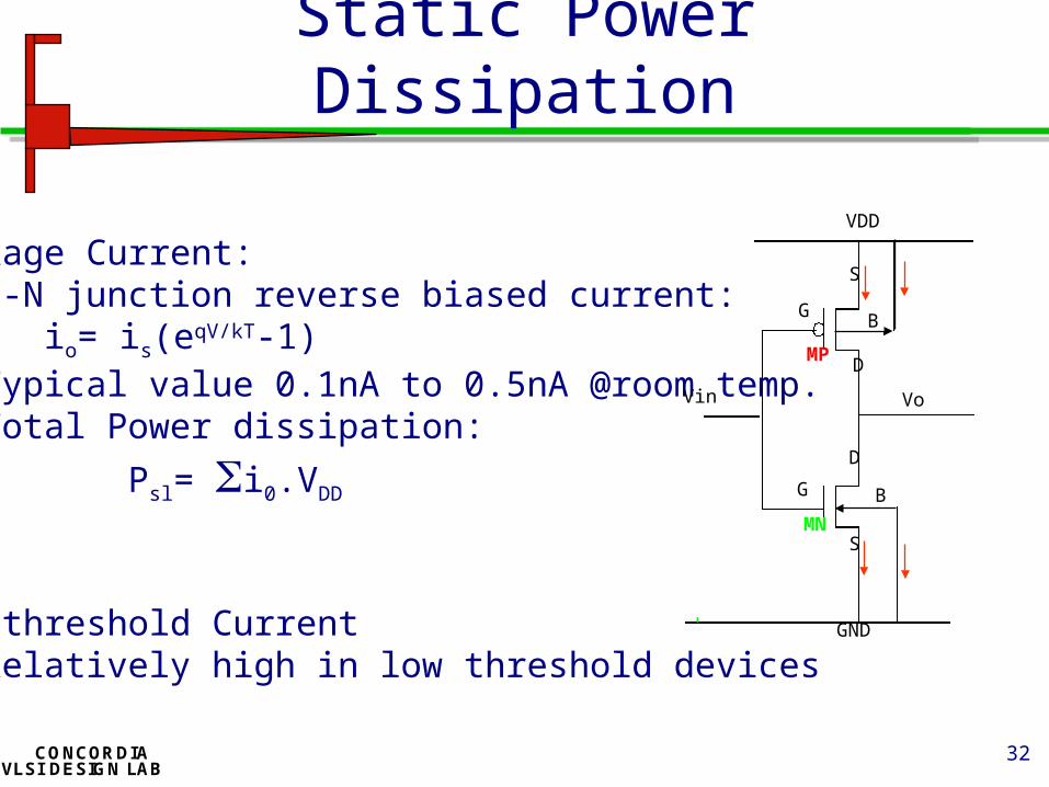
Static Power Dissipation
G
S
D
D
G
S
Vo
VDD
GND
B
B
MP
MN
Leakage Current:• P-N junction reverse biased current: io= is(eqV/kT-1) • Typical value 0.1nA to 0.5nA @room temp.• Total Power dissipation:
Psl= i0.VDD
Sub-threshold Current• Relatively high in low threshold devices
Vin
33CONCORDIAVLSI DESIGN LAB
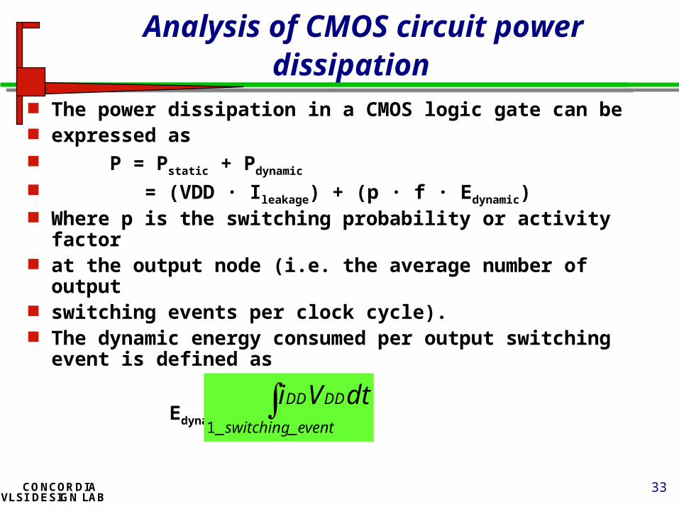
Analysis of CMOS circuit power dissipation
The power dissipation in a CMOS logic gate can be expressed as P = Pstatic + Pdynamic
= (VDD · Ileakage) + (p · f · Edynamic) Where p is the switching probability or activity factor at the output node (i.e. the average number of output switching events per clock cycle). The dynamic energy consumed per output switching
event is defined as
Edynamic = eventswitching
DDDD dtVi__1
34CONCORDIAVLSI DESIGN LAB
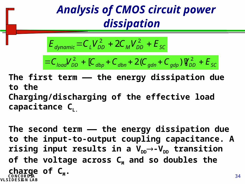
Analysis of CMOS circuit power dissipation
SCDDMDDLdynamic EVCVCE 22 2
SCDDgdpgdndbndbpDDload EVCCCCVC 22 )](2[
The first term —— the energy dissipation due to theCharging/discharging of the effective load capacitance CL.
The second term —— the energy dissipation due to the input-to-output coupling capacitance. A rising input results in a VDD-VDD transition of the voltage across CM and so doubles the charge of CM.
CL = Cload + Cdbp +Cdbn
CM = Cgdn + Cgdp

35CONCORDIAVLSI DESIGN LAB
• distributed, • voltage-dependent, and • nonlinear. So their exact modeling is quite complex.
The MOSFET parasitic capacitances
Even ESC can be modeled, it is also difficult to calculate the Edynamic.
On the other hand, if the short-circuit current iSC can be Modeled, the power-supply current iDD may be modeled with the same method.
So there is a possibility to directly model iDD instead of iSC.

36CONCORDIAVLSI DESIGN LAB
Schematic of the Inverter

37CONCORDIAVLSI DESIGN LAB

38CONCORDIAVLSI DESIGN LAB
The short-circuit energy dissipation ESC is due to the rail-to-rail current when both the PMOS and NMOS devices are simultaneously on.
ESC = ESC_C + ESC_n
Where
and
DDVv
nDDcSC dtiVE0
_
0
0
_
0 DDVv
pDDdSC dtiVE
Analysis of short-circuit current

39CONCORDIAVLSI DESIGN LAB
Charging and discharging currents
Discharging Inverter Charging Inverter

40CONCORDIAVLSI DESIGN LAB
Factors that affect the short-circuit current
TVV
VI TDD
DDmean
3)2(12
1
For a long-channel device, assuming that the inverter is symmetrical (n = p = and VTn = -VTp = VT) and with zero load capacitance, and input signal has equal rise and fall times (r = f = ), the average short-circuit current [Veendrick, 1994] is
From the above equation, some fundamental factors that affect short-circuit current are:
, VDD, VT, and T.)(L
W
tox

41CONCORDIAVLSI DESIGN LAB
Parameters affecting short cct current
For a short-channel device, and VT are no longer constants, but affected by a large number of parameters (i.e. circuit conditions, hspice parameters and process parameters).
CL also affects short-circuit current.
Imean is a function of the following parameters (tox is process-dependent): CL, , T (or /T), VDD, Wn,p, Ln,p (or Wn,p/ Ln,p ), tox, …
The above argument is validated by the means of simulation in the case of discharging inverter,

42CONCORDIAVLSI DESIGN LAB
The effect of CL on Short CCt Current

43CONCORDIAVLSI DESIGN LAB
Effect of tr on short cct Current

44CONCORDIAVLSI DESIGN LAB
Effect of Wp on Short cct Current

45CONCORDIAVLSI DESIGN LAB
Effect of timestep setting on simulation results
Tr (ps) Timestep (ps) MaxStep (ps) iMax (uA) iaverage_inT/2 (uA) 2 10 802.6 1.258 4 10 413.8 1.264 5 10 336.4 1.24 6 10 284.9 1.234 8 10 221 1.245
0
10 20 183 1.231 2 10 73.09 1.202 4 10 64.4 1.213 5 10 58.69 1.21 6 10 65.64 1.208 8 10 76.13 1.207
100
10 20 63.1 1.217 2 10 50.96 1.311 5 10 49.78 1.295 5 20 50.46 1.313 8 10 50.72 1.311 8 20 52.08 1.311
200
10 20 51.25 1.311

46CONCORDIAVLSI DESIGN LAB
Thank you !