2812 ieee journal of solid-state circuits, vol....
TRANSCRIPT
2812 IEEE JOURNAL OF SOLID-STATE CIRCUITS, VOL. 49, NO. 12, DECEMBER 2014
A 1.1 nW Energy-Harvesting System with 544 pWQuiescent Power for Next-Generation ImplantsSaurav Bandyopadhyay, Member, IEEE, Patrick P. Mercier, Member, IEEE, Andrew C. Lysaght,
Konstantina M. Stankovic, and Anantha P. Chandrakasan, Fellow, IEEE
Abstract—This paper presents a nW power management unit(PMU) for an autonomous wireless sensor that sustains itselfby harvesting energy from the endocochlear potential (EP), the70–100 mV electrochemical bio-potential inside the mammalianear. Due to the anatomical constraints inside the inner ear, the totalextractable power from the EP is limited close to 1.1–6.25 nW.A nW boost converter is used to increase the input voltage(30–55 mV) to a higher voltage (0.8–1.1 V) usable by CMOS cir-cuits in the sensor. A pW charge pump circuit is used to minimizethe leakage in the boost converter. Furthermore, ultralow-powercontrol circuits consisting of digital implementations of inputimpedance adjustment circuits and zero current switching circuitsalong with Timer and Reference circuits keep the quiescent powerof the PMU down to 544 pW. The designed boost converterachieves a peak power conversion efficiency of 56%. The PMUcan sustain itself, and a duty-cyled ultralow-power load whileextracting power from the EP of a live guinea pig. The PMUcircuits have been implemented on a 0.18- m CMOS process.
Index Terms—Boost converter, charge pump, endo-cochlear po-tential (EP), energy harvesting, low-power design.
I. INTRODUCTION
B IOMEDICAL implantable electronic systems like pace-makers and cochlear implants are being used extensively
today, and devices like retinal implants and intracranial pressuresensors are also being developed [1]. Moreover, a wide range ofimplants are now being envisioned for sensing, in-vivo drug de-livery, and other applications [2], [4]. Typically, these implants
Manuscript received April 21, 2014; revised June 27, 2014; accepted July30, 2014. Date of publication September 19, 2014; date of current versionNovember 20, 2014. This paper was approved by Guest Editor MakotoNagata. This work was supported in part by the C2S2 Focus Center and theInterconnect Focus Center, two of six research centers funded under the FocusCenter Research Program (FCRP), a Semiconductor Research Corporationentity, by the National Institutes of Health under Grants K08 DC010419 andT32 DC00038, and by the Bertarelli Foundation.S. Bandyopadhyay was with theMassachusetts Institute of Technology, Cam-
bridge, MA USA. He is now with Texas Instruments, Dallas, TX 75243 USA(e-mail: [email protected]).P. P. Mercier is with the University of California at San Diego, La Jolla, CA
92093-0407 USA.A. C. Lysaght is with the Massachusetts Eye and Ear Infirmary, Boston, MA
02114 USA.K. M. Stankovic is with MEEI, Massachusetts General Hospital, Harvard
Medical School, Boston, MA 02114 USA.A. P. Chandrakasan is with the Massachusetts Institute of Technology, Cam-
bridge, MA 02139 USA.Color versions of one or more of the figures in this paper are available online
at http://ieeexplore.ieee.org.Digital Object Identifier 10.1109/JSSC.2014.2350260
are powered by batteries that either need to be replaced periodi-cally or need to be chargedwirelessly [3]. However, stringent re-strictions on the battery electrolytes’ containments and on tissueheating [3] make achieving energy autonomy extremely chal-lenging in such implantable systems.Traditional energy harvesters like photo-voltaic cells, ther-
moelectric generators, and piezoelectric harvesters as describedin [5] are not ideal for implantable electronics since these en-ergy sources require conditions that typically do not exist in-side a mammalian body. The endocochlear potential (EP) is a70–100 mV dc bio-potential [6], [7] that exists inside the mam-malian cochlea. It has been demonstrated that, by utilizing theEP as the sole energy source, it is possible to power an ul-tralow-power implant inside the inner ear that can be used forsensing and in-vivo drug delivery [8]. Due to anatomical con-straints inside the inner ear, the total extractable power from theEP is limited close to 1.1–6.25 nW. While the work presentedin [8] focuses on the biological aspects of the proposed conceptand the high-level sensor definition, this paper focuses on thecircuit details of the nW power management unit (PMU) [9] thatenabled the proposed sensor and powered an ultralow-power,duty-cycled RF transmitter [10] in the sensor.In order to operate the PMU at nW levels, there are some
key circuit design challenges that need to be addressed. First,the PMU needs to be as efficient as possible while processingultralow power. Second, the PMU control circuits need to bealways active, making it necessary to reduce the quiescentcurrent in these circuits to ensure system sustainability. Third,we need to ensure that close to maximum available power isextracted from the energy source at all times. Although thePMU is designed assuming EP to be the energy source in thiswork, all of the circuit techniques that will be presented herecan be easily extended to all low-power energy-harvestingsystems. This paper is organized as follows. Section II high-lights the PMU architecture. Section III focuses on the nWboost converter operation, design, and optimization. Section IVhighlights the pW charge pump circuit used to minimize theleakage power in the boost converter. Section V presents thepW control, timer, and reference circuits that enabled the sensoroperation. Section VI highlights the simulated performance ofthe PMU under process variations. Section VII focuses on thePMU measured results.
II. PMU ARCHITECTURE
The PMU, shown in Fig. 1, consists of a nW boost converter,pW control circuits ( and generation circuits), a chargepump along with timer and reference circuits. Two electrodes
0018-9200 © 2014 IEEE. Personal use is permitted, but republication/redistribution requires IEEE permission.See http://www.ieee.org/publications_standards/publications/rights/index.html for more information.

BANDYOPADHYAY et al.: 1.1 nW ENERGY-HARVESTING SYSTEM WITH 544 pW QUIESCENT POWER FOR NEXT-GENERATION IMPLANTS 2813
Fig. 1. Diagram of the nW PMU.
connected to the PMU are inserted into the inner ear to tap theEP. Due to the anatomical constraints in the inner ear, these elec-trodes need to have tip diameters close to 2 m [8], causing theresistance of each electrode to be around 200–600 k . The en-ergy source can therefore be modelled by a voltage sourceand a series resistor , which is the sum of the two electroderesistances [8]. With an overall electrode impedance of 400 kto 1.2 M and of 70–100 mV, the maximum extractedpower from the EP , is close to 1–6.25 nW. Thisis much lower than the power budget of previously publishedPMUs [11]–[13]. Further, the input voltage for the boost con-verter is half the EP (about 30–55 mV) when maximum poweris extracted.This implies that we need an efficient boost converter that op-
erates with input voltages from 30 to 55 mV and can boost it upto 0.8–1.1 V, which are voltages that are more usable by CMOScircuits, at nW power levels. The high voltage-conversion ratioalong with the nW power budget make achieving high efficien-cies extremely challenging. The boost converter in this workhas been designed to meet the aforementioned requirements. Acharge pump has been employed to reduce leakage in the boostconverter. To ensure system sustainability, the quiescent powerof all control, timer, and reference circuits have been kept in thetens to hundreds of pW range.
III. ULTRALOW-POWER BOOST CONVERTER DESIGNAND OPTIMIZATION
A. Ultralow-Power Boost Converter Operation
Due to the ultralow-power budget, the boost converter usedin the PMU operates in the discontinuous conduction mode(DCM). While extracting maximum power, the input voltageis typically close to half of the EP, as shown in Fig. 2(a).
Fig. 2. Boost converter operation. (a) Boost converter trickle charging systempower supply. (b) Boost converter operation on a cycle-by-cycle basis.
Therefore, the converter is required to boost up an input voltageof 30–55 mV up to 0.8–1.1 V which is used
to power the control and timer circuits, a charge pump, anda duty-cycled load (RF-Tx in this work). The RF-Tx loadis periodically enabled [once every 40–360 s, as shown inFig. 2(a)] causing the boost converter output voltageto droop instantaneously. The starts to rise up once theRF-Tx load is disabled. This ensures that the converter is able toaccumulate sufficient energy from the EP to be able to turn onthe RF-Tx load for a short burst. The cycle-by-cycle operationof the boost converter has been shown in Fig. 2(b). During thephase, the NMOS power FET ( in Fig. 1) is on, and the
current through the inductor ramps up, storing energy in theinductor. After a fixed time (e.g., 2.5 s, justified later inSection V), is turned off and the PMOS power FET ( in
2814 IEEE JOURNAL OF SOLID-STATE CIRCUITS, VOL. 49, NO. 12, DECEMBER 2014
Fig. 1) is turned on for time , causing the energy stored in theinductor to be transferred to the system power supply capacitor
. Since the converter operates in DCM, after the phase,the converter stays idle until the phase of the next switchingcycle. This idle phase is much longer thanphases and primarily due to the low input current to theconverter.In traditional energy-harvesting systems [14], [15], there
are usually two power converters in series between the energysource and the load circuits. The first power converter regulatesthe input voltage (or adjusts the input impedance for maximumpower transfer), storing the harvested energy on to an energybuffer (supercapacitor or battery), and the second converterregulates the output voltage to the load circuits. However,due to the stringent power budget in this PMU, a single boostconverter has been used. The converter has an input impedanceclose to the electrode impedance in order to ensure that closeto maximum power is transferred from the EP. The output ofthe converter is unregulated and settles to a level where thesum of the losses in the boost converter and power dissipatedin the control and load circuits equals the power harvestedby the boost converter (0.8–1.1 V in this implementation).For a variety of sensing applications, the load, usually RF-Txcircuits, can be aggressively power-gated and duty-cycled.These circuits need to make infrequent RF transmissions andthen can be idle for long periods of time. Therefore, dependingon the input power to the PMU, the frequency of triggering theRF load can be varied to coarsely adjust the output voltage. Ifthe input power is high, the duty-cycled load can be triggeredmore frequently and vice versa. In this implementation, thefrequency of triggering the load is adjusted by externallyconfiguring 2 bits as the electrode impedance is known beforeimplantation (explained later in more detail in Section V).Previous work [16] has shown that for boost converters in
DCM, operating with a high voltage-conversion ratio, the inputimpedance (ratio of input voltage to average input current) isapproximately given by
(1)
where is the on time, is the switching frequency, andis the converter’s inductor. Therefore, In this work, on
time, switching frequency, and the boost converter inductancehave been selected such that the input impedance of the boostconverter is close to the sum of the electrode resistances. Thiswill be discussed in more detail later.
B. Ultralow-Power Boost Converter Design Considerations
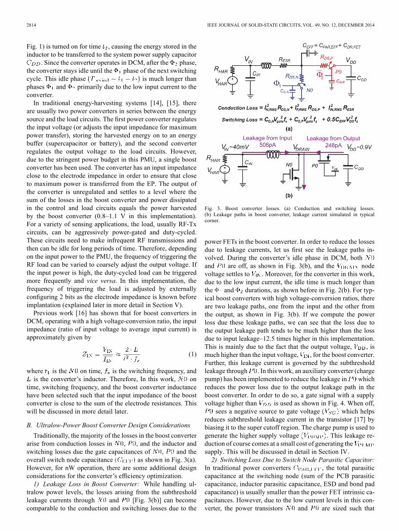
Traditionally, the majority of the losses in the boost converterarise from conduction losses in , , and the inductor andswitching losses due the gate capacitances of , and theoverall switch node capacitance as shown in Fig. 3(a).However, for nW operation, there are some additional designconsiderations for the converter’s efficiency optimization.1) Leakage Loss in Boost Converter: While handling ul-
tralow power levels, the losses arising from the subthresholdleakage currents through and [Fig. 3(b)] can becomecomparable to the conduction and switching losses due to the
Fig. 3. Boost converter losses. (a) Conduction and switching losses.(b) Leakage paths in boost converter, leakage current simulated in typicalcorner.
power FETs in the boost converter. In order to reduce the lossesdue to leakage currents, let us first see the leakage paths in-volved. During the converter’s idle phase in DCM, bothand are off, as shown in Fig. 3(b), and the nodevoltage settles to . Moreover, for the converter in this work,due to the low input current, the idle time is much longer thanthe and durations, as shown before in Fig. 2(b). For typ-ical boost converters with high voltage-conversion ratios, thereare two leakage paths, one from the input and the other fromthe output, as shown in Fig. 3(b). If we compute the powerloss due these leakage paths, we can see that the loss due tothe output leakage path tends to be much higher than the lossdue to input leakage–12.5 times higher in this implementation.This is mainly due to the fact that the output voltage, , ismuch higher than the input voltage, , for the boost converter.Further, this leakage current is governed by the subthresholdleakage through . In this work, an auxiliary converter (chargepump) has been implemented to reduce the leakage in whichreduces the power loss due to the output leakage path in theboost converter. In order to do so, a gate signal with a supplyvoltage higher than is used as shown in Fig. 4. When off,
sees a negative source to gate voltage which helpsreduces subthreshold leakage current in the transistor [17] bybiasing it to the super cutoff region. The charge pump is used togenerate the higher supply voltage . This leakage re-duction of course comes at a small cost of generating thesupply. This will be discussed in detail in Section IV.2) Switching Loss Due to Switch Node Parasitic Capacitor:
In traditional power converters , the total parasiticcapacitance at the switching node (sum of the PCB parasiticcapacitance, inductor parasitic capacitance, ESD and bond padcapacitance) is usually smaller than the power FET intrinsic ca-pacitances. However, due to the low current levels in this con-verter, the power transistors and are sized such that

BANDYOPADHYAY et al.: 1.1 nW ENERGY-HARVESTING SYSTEM WITH 544 pW QUIESCENT POWER FOR NEXT-GENERATION IMPLANTS 2815
Fig. 4. Leakage reduction by negative source-to-gate bias.
becomes more than the intrinsic FET capacitances.Following the phase of the boost converter, the commondrain terminal of and rings due to the resonant circuitformed by , and as shown in Fig. 2(b). Duringthis ringing, the stored energy in is partly dissipatedin the body diode of ( rings and goes a diode voltagebelow ground turning on the body diode) and in the inductorduring the idle time of the boost converter. To get a quantita-tive idea, let’s consider a typical value of 5 pF for .At a typical switching frequency of 1 kHz and 1 V , thiswould cause 2.5 nW loss, which is more than the system powerbudget’s lower limit by 2.27 times and is 40% of the systempower budget’s upper limit. Further, it must be noted that, de-pending on the board layout and the type of inductor, it mightbe difficult to control this parasitic capacitance. Therefore, theswitching frequency of the converter needs to be appropriatelyselected.Therefore, keeping the leakage currents in the power train
and the parasitic capacitances in mind, the boost converter hasbeen optimized. These two key aspects along with the inputimpedance requirement make converter’s efficiency optimiza-tion different from previously published low power switchingconverters [12], [15].
C. Loss Optimization
The following equation gives the approximate expression forthe sum of the different losses in the boost converter-gate drivelosses (due to and with the Miller Effect), FET con-duction losses, conduction loss due to inductor ESR, and FETleakage losses:
(2)
where , , and are the gate-to-drain and gate-to-source capacitances per unit width for and, and are the corresponding transistor widths, is
the efficiency of the charge pump, is the peak inductor cur-rent, and are the resistance per unit width for and, and are the leakage currents per unit
width of and , is the effective series resistanceof the inductor, and and are theleakage currents in the and gate drivers per unit width of
and . The FET drain to source capacitances along withcan be all absorbed into . It must be noted that
the loss due to the Miller-effected capacitance appears only forsince the switch node gets charged up to
by the inductor current if there is adequate dead-time betweenturning off and turning on . Moreover, the miller capac-itance due to gets multiplied by the of
which is in DCM. Further, since a boost converterwith high voltage-conversion ratios is being optimized, on ap-proximating the inductor’s volt-second rule, we can relateand by . We also know thatand . By imposing the impedance conditiongiven by (1), along with (2), we can simplify the conduction lossterms (for , and inductor ESR) and make the approxima-tion that is much greater than for the boost converterin this work to give us
2816 IEEE JOURNAL OF SOLID-STATE CIRCUITS, VOL. 49, NO. 12, DECEMBER 2014
(3)
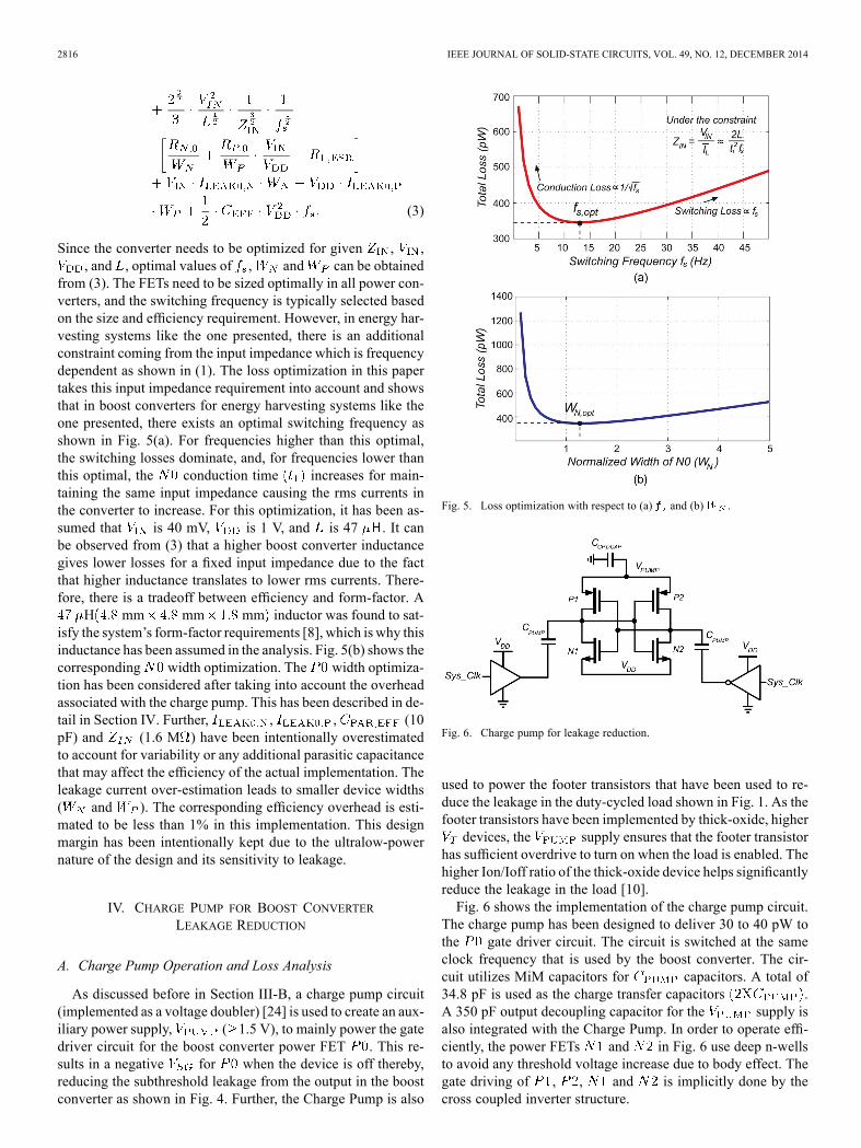
Since the converter needs to be optimized for given , ,, and , optimal values of , and can be obtained
from (3). The FETs need to be sized optimally in all power con-verters, and the switching frequency is typically selected basedon the size and efficiency requirement. However, in energy har-vesting systems like the one presented, there is an additionalconstraint coming from the input impedance which is frequencydependent as shown in (1). The loss optimization in this papertakes this input impedance requirement into account and showsthat in boost converters for energy harvesting systems like theone presented, there exists an optimal switching frequency asshown in Fig. 5(a). For frequencies higher than this optimal,the switching losses dominate, and, for frequencies lower thanthis optimal, the conduction time increases for main-taining the same input impedance causing the rms currents inthe converter to increase. For this optimization, it has been as-sumed that is 40 mV, is 1 V, and is 47 . It canbe observed from (3) that a higher boost converter inductancegives lower losses for a fixed input impedance due to the factthat higher inductance translates to lower rms currents. There-fore, there is a tradeoff between efficiency and form-factor. A
H mm mm mm inductor was found to sat-isfy the system’s form-factor requirements [8], which is why thisinductance has been assumed in the analysis. Fig. 5(b) shows thecorresponding width optimization. The width optimiza-tion has been considered after taking into account the overheadassociated with the charge pump. This has been described in de-tail in Section IV. Further, , , (10pF) and (1.6 M ) have been intentionally overestimatedto account for variability or any additional parasitic capacitancethat may affect the efficiency of the actual implementation. Theleakage current over-estimation leads to smaller device widths( and ). The corresponding efficiency overhead is esti-mated to be less than 1% in this implementation. This designmargin has been intentionally kept due to the ultralow-powernature of the design and its sensitivity to leakage.
IV. CHARGE PUMP FOR BOOST CONVERTERLEAKAGE REDUCTION
A. Charge Pump Operation and Loss Analysis
As discussed before in Section III-B, a charge pump circuit(implemented as a voltage doubler) [24] is used to create an aux-iliary power supply, ( 1.5 V), to mainly power the gatedriver circuit for the boost converter power FET . This re-sults in a negative for when the device is off thereby,reducing the subthreshold leakage from the output in the boostconverter as shown in Fig. 4. Further, the Charge Pump is also
Fig. 5. Loss optimization with respect to (a) and (b) .
Fig. 6. Charge pump for leakage reduction.
used to power the footer transistors that have been used to re-duce the leakage in the duty-cycled load shown in Fig. 1. As thefooter transistors have been implemented by thick-oxide, higherdevices, the supply ensures that the footer transistor
has sufficient overdrive to turn on when the load is enabled. Thehigher Ion/Ioff ratio of the thick-oxide device helps significantlyreduce the leakage in the load [10].Fig. 6 shows the implementation of the charge pump circuit.
The charge pump has been designed to deliver 30 to 40 pW tothe gate driver circuit. The circuit is switched at the sameclock frequency that is used by the boost converter. The cir-cuit utilizes MiM capacitors for capacitors. A total of34.8 pF is used as the charge transfer capacitors .A 350 pF output decoupling capacitor for the supply isalso integrated with the Charge Pump. In order to operate effi-ciently, the power FETs and in Fig. 6 use deep n-wellsto avoid any threshold voltage increase due to body effect. Thegate driving of , , and is implicitly done by thecross coupled inverter structure.

BANDYOPADHYAY et al.: 1.1 nW ENERGY-HARVESTING SYSTEM WITH 544 pW QUIESCENT POWER FOR NEXT-GENERATION IMPLANTS 2817
It must be noted that, while optimizing the power conversionefficiency of the charge pump, the subthreshold leakage cur-rents in the charge pump need to be taken into account. Fig. 7shows the current paths through and the leakage cur-rent in the charge pump during the two clock phases, directionof switching currents ( and ) has been shown in blueand the leakage currents ( through ) in red. Thecurrents charging up the gate capacitances of , , and
have not been shown for simplicity. The total output currentfrom the supply is given by
(4)
and the total input current from is given by
(5)
where is the ratio of bottom plate parasitic capacitance to theactual capacitance and is the total switching effective gatecapacitance due to the , , and .Therefore, the efficiency of the converter can be expressed as
in
(6)
with terms and which have been defined in (7) and (8),respectively, shown at the bottom of the page.Equation (6) is similar to the efficiency expression for the
conventional 1:2 voltage conversion charge pump except forthe fact that the terms and account for the leakage andparasitic capacitors. The power conversion efficiency hasbeen optimized to around 77% in this implementation. Sincethe converter switches at 12.8 Hz, it operates well within itsslow-switching limit [25]. Therefore, the devices have beensized essentially to minimize leakage while providing therequired speed by following the methodology in [26]. Due tothe ultra-low power requirement, the capacitors hasbeen intentionally over-sized to account variations in leakagecurrent through the doubler circuit transistors or in the gatedrive circuit which is the load circuit for the doubler. Higher
would enable us to suppress the variations in leakage inthe charge pump [(7) and (8)] and would also help in supplying
Fig. 7. Current paths charge pump in (a) and(b) .
Fig. 8. Lower minimum loss achieved by charge pump.
more current to the gate drive circuit (4). Over-sizingresults in about 4 pW of extra switching loss.
B. Leakage Reduction, Net Power Savings, and Sizing
For this implementation, because of the charge pump, theleakage power due to subthreshold leakage in is reduced
(7)
(8)
2818 IEEE JOURNAL OF SOLID-STATE CIRCUITS, VOL. 49, NO. 12, DECEMBER 2014
Fig. 9. Pulse generators for and phases of boost converter.
from 224 pW (simulated without charge pump) to as low as0.75 pW (simulated with charge pump) at the typical corner.This comes at the cost of increased switching loss and leakagein the gate drive circuit due to higher supply voltage. Thisoverhead is estimated to be 30–40 pW. On factoring in the effi-ciency of the charge pump, this overhead becomes 39 to 52 pW.Without the charge pump, the gate drive circuit would have con-sumed 4 pW. Therefore, an overall benefit of 175 to 188 pW(simulated) is obtained. Although it may seem a small amount,this power reduction is close to 17% of the minimum systempower budget. Moreover, in the fast corner, a net power savingof about 950 pW is obtained indicating that the charge pump en-ables the PMU operation for all process corners. One may con-sider reducing the leakage in the boost converter power FETby simply reducing its width. In this case, the FET size needsto be done by minimizing the sum of conduction, switching andleakage losses as shown by the red plot in Fig. 8. However, fromthe optimization analysis done before in Section III-C, it is ob-served that, after accounting for the overhead associated withthe charge pump, this technique results in a lower minimumloss (124.7 pW lower, which is 12.4% of the input power inthis analysis). Fig. 8 also shows that this technique enables usto use wider device with lower conduction losses and lowerleakage. Therefore, the charge pump becomes essential for en-suring ultra-low power operation of the PMU.
V. CONTROL, TIMER, REFERENCE, AND STARTUP CIRCUITS
In order for the PMU to sustain itself, all of the control circuitsand drivers have been designed to consume less than the energyharvested by the boost converter. The control circuits consistsof circuits ensuring maximum power extraction (shown asGeneration in Fig. 1), ZCS control for DCM (shown as Gen-eration in Fig. 1), and Timer with references.
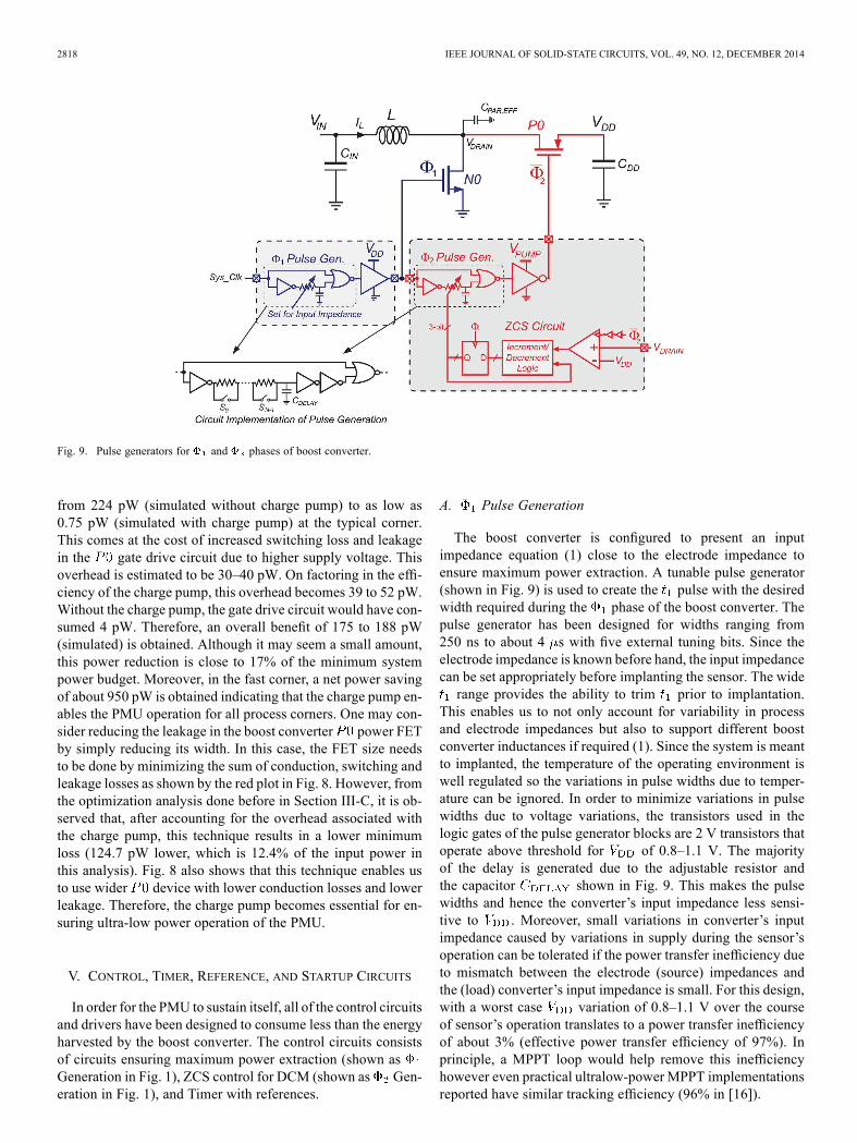
A. Pulse Generation
The boost converter is configured to present an inputimpedance equation (1) close to the electrode impedance toensure maximum power extraction. A tunable pulse generator(shown in Fig. 9) is used to create the pulse with the desiredwidth required during the phase of the boost converter. Thepulse generator has been designed for widths ranging from250 ns to about 4 s with five external tuning bits. Since theelectrode impedance is known before hand, the input impedancecan be set appropriately before implanting the sensor. The widerange provides the ability to trim prior to implantation.
This enables us to not only account for variability in processand electrode impedances but also to support different boostconverter inductances if required (1). Since the system is meantto implanted, the temperature of the operating environment iswell regulated so the variations in pulse widths due to temper-ature can be ignored. In order to minimize variations in pulsewidths due to voltage variations, the transistors used in thelogic gates of the pulse generator blocks are 2 V transistors thatoperate above threshold for of 0.8–1.1 V. The majorityof the delay is generated due to the adjustable resistor andthe capacitor shown in Fig. 9. This makes the pulsewidths and hence the converter’s input impedance less sensi-tive to . Moreover, small variations in converter’s inputimpedance caused by variations in supply during the sensor’soperation can be tolerated if the power transfer inefficiency dueto mismatch between the electrode (source) impedances andthe (load) converter’s input impedance is small. For this design,with a worst case variation of 0.8–1.1 V over the courseof sensor’s operation translates to a power transfer inefficiencyof about 3% (effective power transfer efficiency of 97%). Inprinciple, a MPPT loop would help remove this inefficiencyhowever even practical ultralow-power MPPT implementationsreported have similar tracking efficiency (96% in [16]).
BANDYOPADHYAY et al.: 1.1 nW ENERGY-HARVESTING SYSTEM WITH 544 pW QUIESCENT POWER FOR NEXT-GENERATION IMPLANTS 2819
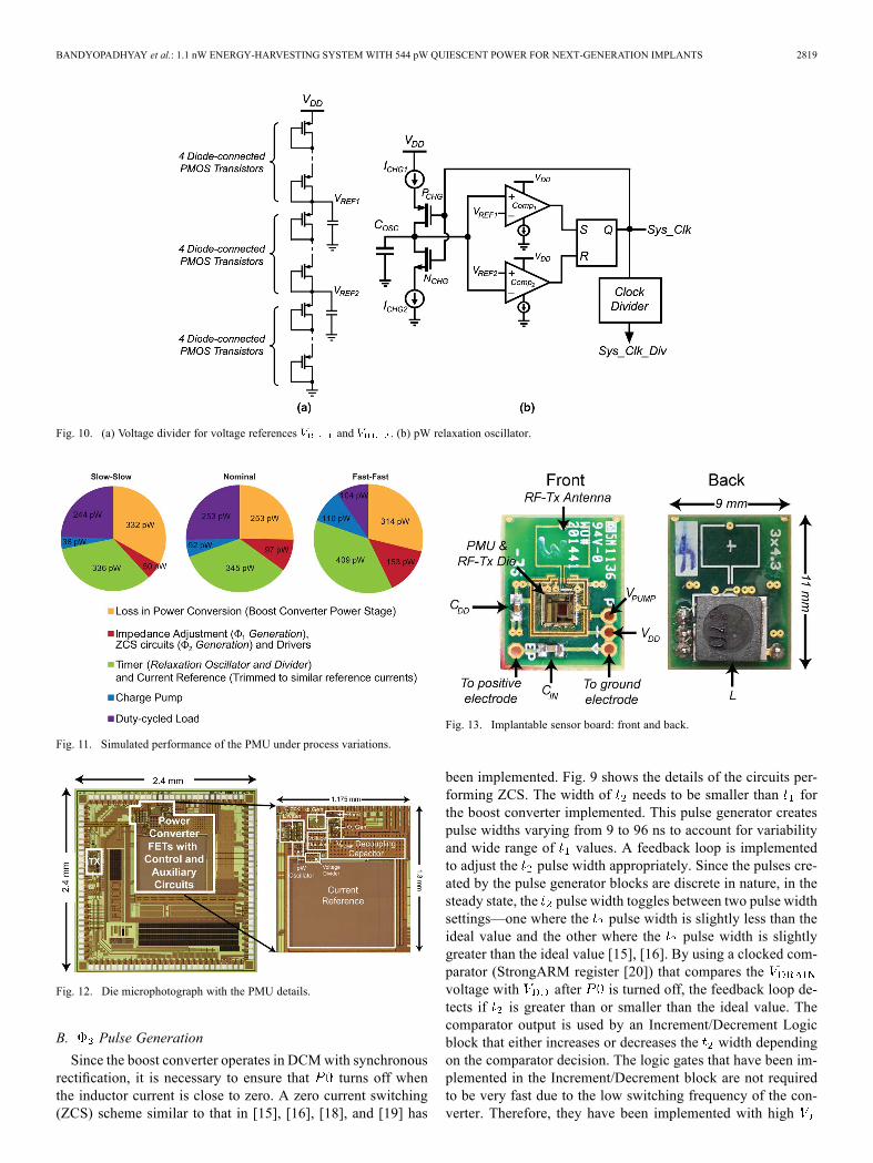
Fig. 10. (a) Voltage divider for voltage references and . (b) pW relaxation oscillator.
Fig. 11. Simulated performance of the PMU under process variations.
Fig. 12. Die microphotograph with the PMU details.
B. Pulse Generation
Since the boost converter operates in DCMwith synchronousrectification, it is necessary to ensure that turns off whenthe inductor current is close to zero. A zero current switching(ZCS) scheme similar to that in [15], [16], [18], and [19] has
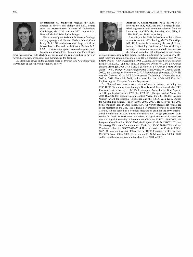
Fig. 13. Implantable sensor board: front and back.
been implemented. Fig. 9 shows the details of the circuits per-forming ZCS. The width of needs to be smaller than forthe boost converter implemented. This pulse generator createspulse widths varying from 9 to 96 ns to account for variabilityand wide range of values. A feedback loop is implementedto adjust the pulse width appropriately. Since the pulses cre-ated by the pulse generator blocks are discrete in nature, in thesteady state, the pulse width toggles between two pulse widthsettings—one where the pulse width is slightly less than theideal value and the other where the pulse width is slightlygreater than the ideal value [15], [16]. By using a clocked com-parator (StrongARM register [20]) that compares thevoltage with after is turned off, the feedback loop de-tects if is greater than or smaller than the ideal value. Thecomparator output is used by an Increment/Decrement Logicblock that either increases or decreases the width dependingon the comparator decision. The logic gates that have been im-plemented in the Increment/Decrement block are not requiredto be very fast due to the low switching frequency of the con-verter. Therefore, they have been implemented with high
2820 IEEE JOURNAL OF SOLID-STATE CIRCUITS, VOL. 49, NO. 12, DECEMBER 2014
Fig. 14. Boost converter results for different EP voltages: (a) measured power v/s input voltage, (b) measured efficiency versus input voltage, and (c) measurementsetup.
transistors, operating in subthreshold with long gate lengths tominimize leakage currents.
C. Timer and Reference Circuits
A pW relaxation oscillator similar to [21] and a clock dividerhave been implemented as timer circuits [Fig. 10(b)]. The oscil-lator is designed to generate a 12.8 Hz clock , withfrequency close to the optimal for the boost converter. Theclock divider creates a lower frequency clockfrom which is used to enable the RF-Tx once in40–360 s. Two analog comparators and (dif-ferential amplifier stage followed by common source stage), areused to compare the voltage across with two referencevoltages, and . References and areset to and , respectively, by a voltage dividerformed by cascading twelve PMOS transistors biased in thesubthreshold regime [Fig. 10(a)]. Currents , andthe analog comparator bias currents are mirrored from the asupply independent current reference [22], [23] with 60 pAreference current.
D. Low-Voltage Startup
Some previously published works have demonstrated low-voltage startup using MEMs switches [15], silicon post pro-cessing [27], transformers with normally on transistors [28], andstartup ring oscillators [12]. Most of these techniques have spe-cial requirements from the technology used [15], [27], [28] or
are limited to startup voltages in hundreds of mV [12]. In thiswork, it is envisioned that the sensor can be started up by wire-less means after it has been implanted. An external transmitter isused to transfer an initial burst of energy to the sensor. The sameantenna used by the RF-Tx in the sensor is utilized to receivethis energy burst. The ESD diodes rectify the ac voltage andcharging the power supply [8], [10]. This initial charge up( getting charged to 0.9 V observed to be sufficient) startsup the pW relaxation oscillator in the system. Since the oscil-lator clock directly goes to the boost converter and gen-eration circuits and the charge pump, both the boost converterand the Charge Pump start up. Moreover, the bits for pulsewidth are set before implantation so the generation circuit(Fig. 9) starts up from a known state. For the generation cir-cuit, there are 3 registers that hold the pulse width information(Fig. 9). In case these registers start up in the wrong state, sincethere is a ZCS feedback loop, in the worst case this would takenine cycles to correct itself. In this implementation, this wasfound to not effect the system performance.
VI. SYSTEM SIMULATION WITH PROCESS VARIATIONS
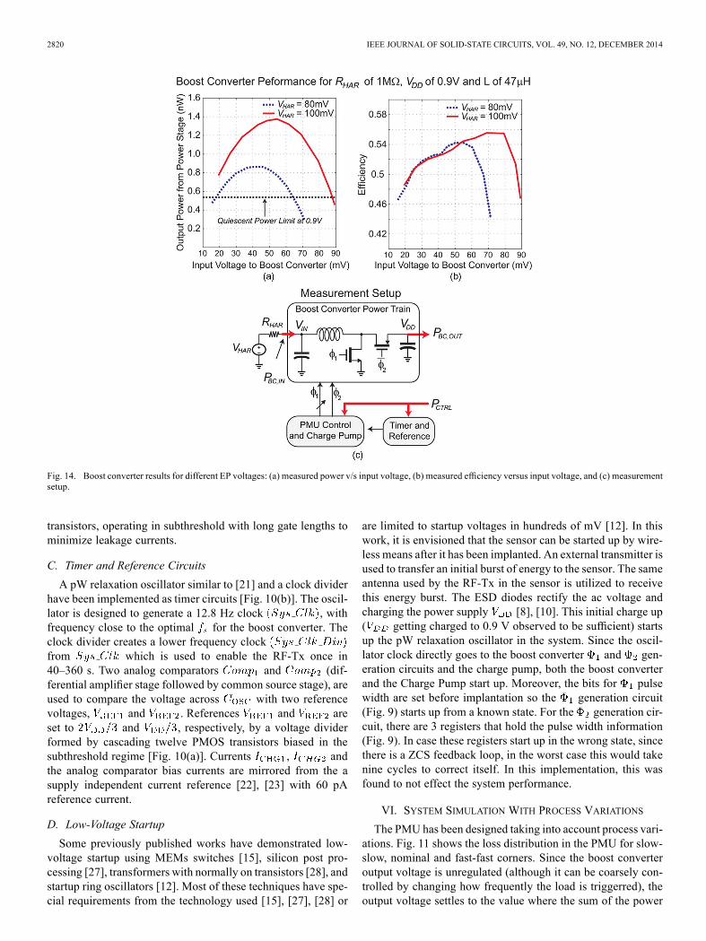
The PMU has been designed taking into account process vari-ations. Fig. 11 shows the loss distribution in the PMU for slow-slow, nominal and fast-fast corners. Since the boost converteroutput voltage is unregulated (although it can be coarsely con-trolled by changing how frequently the load is triggerred), theoutput voltage settles to the value where the sum of the power

BANDYOPADHYAY et al.: 1.1 nW ENERGY-HARVESTING SYSTEM WITH 544 pW QUIESCENT POWER FOR NEXT-GENERATION IMPLANTS 2821
Fig. 15. Boost converter results with 80 mV EP for different inductors: (a) measured power v/s input voltage, (b) measured efficiency v/s input voltage.
converter’s losses, control and load circuitry power dissipationbecomes equal to the power being harvested by the boost con-verter. For the slow–slow and the nominal corners, the inputpower to the PMU is 1 nW and the outputs settle to 1 and 0.97 V,respectively. However, it is observed that 1 nW is not sufficientfor the system to sustain itself in the fast–fast corner due to in-creased leakage. For the fast–fast corner simulation, the inputpower to the boost converter is 1.09 nW and the output settles to0.78 V. We can also observe that the load power is significantlylowered at this corner due to lower frequency of triggering theRF load.
VII. EXPERIMENTAL RESULTS
The PMU circuits have been implemented in a 0.18 mCMOS process. Fig. 12 shows the die microphotograph withthe PMU details. Most of the active area is occupied by thecurrent reference resistor (470 M for low quiescent cur-rent requirements, implemented as a high-resistivity polyresistor) and the decoupling capacitor for the supply(350 pF). The large decoupling capacitor is to minimize thedroop in the supply during a RF-Tx transmissionas the supply does not use any off-chip capacitors.Fig. 13 shows the implantable sensor board. The board isdesigned to fit into the human mastoid cavity [8]. The onlyoff-chip components are the boost converter inductor (47 H,4.8 mm 4.8 mm 1.8 mm), system supply capacitor(200 nF), input capacitor (1 F), and an antenna (3 mm4.3 mm) for the RF-Tx.
A. Boost Converter Power Stage Output Power and Efficiency
Fig. 14 shows the boost converter power stage performancefor an electrode impedance of 1 M (emulated by a 1 M re-sistor for this measurement) for two different values of the EP[80 and 100 mV, emulated using a voltage source for this mea-surement as shown in Fig. 14(c)] with a of 0.9 V andboost converter inductance of 47 H. The input voltage to theboost converter is varied by changing the input impedance ofthe boost converter (by varying the pulse width), as shownin Fig. 14(c). In order to characterize the boost converter powerstage output power and efficiency, power has been supplied
Fig. 16. Power consumption of individual circuit blocks.
to all of the control circuits using an external power supplyhere. The converter’s power stage efficiency is mea-
sured by taking the ratio of to . It can be ob-served from Fig. 14(a) that maximum power is extracted by theboost converter power stage for voltages close to half of theEP. This is when the converter’s input impedance equals theelectrode impedance. For the boost converter power stage effi-ciency in Fig. 14(b), it is observed that the efficiency tends tobe higher for higher input voltages. This is due to smaller in-ductor peak currents and, therefore, smaller conduction losses.However, for input voltages higher than 60 mV, the efficiencyreduces due to lower input power to the boost converter powerstage as the converter’s input impedance does not match thesource (emulated electrode) impedance. Fig. 15(a) shows theoutput power from the boost converter power stage for an EP of80 mV, electrode impedance of 750 k , of 0.9 V for dif-ferent values of boost converter inductor. Fig. 15(b) shows thecorresponding efficiency plot. It can be observed that the effi-ciency and output power is lower for lower inductance for thesame input impedance is due to higher rms currents.
B. Power Consumption of Individual Blocks
The quiescent power consumption of the individual blockshas been measured. For an input power of close to 1.2 nW (withemulated EP of 80 mV and electrode resistance of 1.28 Mwhich is the maximum electrode impedance that the system canhandle for the given EP voltage), the boost converter efficiencyis observed to be around 53% with around 0.9 V. This

2822 IEEE JOURNAL OF SOLID-STATE CIRCUITS, VOL. 49, NO. 12, DECEMBER 2014
Fig. 17. Short-term transient measurements. (a) measurement. (b) measurement.
Fig. 18. Comparison with state-of-the-art ultralow-power dc–dc converters.
translates to a total output power of 637 pW from the boost con-verter. Fig. 16 shows the power breakup of the individual cir-cuits utilizing this power. Overall, 544 pW is consumed in theconverter’s control circuits (Boost converter Impedance adjust-ment block, ZCS circuits, timer, reference and charge pump).Therefore, the PMU (without the RF-TX load) can sustain itselfwith close to 1.1 nW input power. Careful design of the boostconverter with the supporting control and auxiliary circuits en-sure that the output power from the converter is not only enoughto sustain the converter but can also be used to power duty cy-cled load circuits like a RF-Tx or other potential loads.
C. Supply Voltage Measurements During Surgical Experiments
Measurements have been made with the PMU connected toelectrodes tapping the EP of a anesthetized guinea pig and sup-plying power to an ultralow-power duty-cycled RF-TX [10].Fig. 17(a) shows the measurements made during three sep-arate surgical experiments for EP values of 80–100 mV andelectrode impedances in the range of 400 k to 1M . Fig. 17(b)shows the corresponding measurements. The supplyvoltages droop when the duty-cycled RF-Tx is enabled. For the
measurements made, the RF-Tx is enabled either once in 40 to80 seconds as can be seen in Fig. 17.
D. Comparison With State-of-the-Art Ultralow-PowerDC–DC Converters
Fig. 18 compares this work with state-of-the-art ultralow-power converters [11]–[13]. As can be seen, the converter im-plemented is the lowest power dc–dc converter reported.
VIII. CONCLUSION
In this work, an ultralow-power PMU has been describedthat powers an implantable wireless sensor by extracting energyfrom the EP, a 70–100 mV bio-potential existing in the mam-malian ear. This is the first reported PMU system that can sustainitself by extracting energy from amammalian bio-potential. Thepower budget of the entire system is 1.1–6.25 nW. Low-powercontrol circuits operating at a low voltage (0.8–1.1 V) and alow frequency (12.8 Hz) help keep the quiescent power of all ofthe control circuits down to 544 pW. Using leakage reductiontechniques normally used in low power digital designs using acharge pump, the efficiency of the boost converter is increased.Maximum power point tracking techniques have not been im-plemented in this work since for the required sensor, the har-vester source impedance (electrode impedance here) remainsconstant over time for a given electrode. However, techniquespresented in [16] can be used in conjunction with this designto cater for an energy harvester that requires maximum powerpoint tracking.
REFERENCES[1] D. Hodgins, A. Bertsch, N. Post, M. Frischholz, B. Volckaerts, J.
Spensleym J. M. Wasikiewicz, H. Higgins, F. von Stetten, and L.Kenney, “Healthy aims: Developing new medical implants and di-agnostic equipment,” IEEE Pervasive Computing, vol. 7, no. 1, pp.14–21, Jan. 2008.
[2] R. D. Black, “Recent advances in translational work on implntable sen-sors,” IEEE Sensors J., vol. 11, no. 12, pp. 3171–3182, Dec. 2011.
[3] V. S. Mallela, V. Ilamkumaran, and N. Srinivasa Rao, “Trends in car-diac pacemaker batteries,” J. Indian Pacing Electrophysiol., vol. 4, no.4, pp. 201–212, Oct. 2004.

BANDYOPADHYAY et al.: 1.1 nW ENERGY-HARVESTING SYSTEM WITH 544 pW QUIESCENT POWER FOR NEXT-GENERATION IMPLANTS 2823
[4] B. I. Rapoport, J. T. Kedzierski, and R. Sarpeshkar, “A glucose fuelcell for implantable brain-machine interfaces,” PloS One, vol. 7, no. 6,Jun. 2012, Art. ID e38436.
[5] R. J. M. Vullers, R. van Schaijk, I. Doms, C. Van Hoof, and R. Mertens,“Micropower energy harvesting,” Solid-State Electron., vol. 53, no. 7,pp. 684–693, Jul. 2009.
[6] G. Von Bekesy, “Resting potentials inide the cochlear partition of theguinea pig,” Nature, vol. 169, pp. 241–242, Feb. 1952.
[7] H. Hibino, F. Nin, C. Tsuzuki, and Y. Kurachi, “How is the highlypositive endocochlear potential formed? The specific architecture ofthe stria vascularis and the roles of the ion-transport apparatus,” PflgersArchiv Eur. J. Physiol., no. 459, pp. 521–533, Mar. 2010.
[8] P. P. Mercier, A. C. Lysaght, S. Bandyopadhyay, A. P. Chandrakasan,and K. M. Stankovic, “Energy extraction from the biologic battery inthe inner ear,”Nature Biotechnol., vol. 30, no. 12, pp. 1240–1243, Dec.2012.
[9] S. Bandyopadhyay, P. P. Mercier, A. C. Lysaght, K. M. Stankovic, andA. P. Chandrakasan, “A 1.1 nW energy harvesting system with 544 pWquisecent power for next generation implants,” in IEEE ISSCC Dig.Tech. Papers, 2014, pp. 396–397.
[10] P. P. Mercier, S. Bandyopadhyay, A. C. Lysaght, K. M. Stankovic, andA. P. Chandrakasan, “A 78 pW 1 B/S 2.4 GHz radio transmitter fornear-zero-power sensing applications,” in IEEE ESSCIRC Dig. Tech.Papers, Sep. 2013, pp. 133–136.
[11] G. Chen, H. Ghaed, R. Haque, M. Wieckowski, Y. Kim, G. Kim, D.Fick, D. Kim, M. Seok, K. Wise, D. Blaauw, and D. Sylvester, “Acubic-millimeter energy-autonomous wireless intraocular pressuremonitor,” in IEEE ISSCC Dig. Tech. Papers, 2011, pp. 311–312.
[12] K. Kadirvel, Y. K. Ramadass, U. Lyles, J. Carpenter, V. Ivanov, V.McNeil, A. Chandrakasan, and B. L-.S-. Chan, “A 330 nA energy-har-vesting charger with battery management for solar and thermoelec-tric energy harvesting,” in IEEE ISSCC Dig. Tech. Papers, 2012, pp.106–108.
[13] Texas Instruments TPS62736 Datasheet, “Programmable OutputVoltage Ultra-Low Power Buck Converter With up to 50 mA/200 mAOutput Current.” Mar. 2013.
[14] N. J. Guilar, R. Amirtharajah, P. J. Hurst, and S. H. Lewis, “An energy-aware multiple-input power supply with charge recovery for energyharvesting applications,” in IEEE ISSCC Dig. Tech. Papers, 2009, pp.298–299.
[15] Y. K. Ramadass and A. P. Chandrakasan, “A battery-less thermoelec-tric energy harvesting interface circuit with 35 mV startup voltage,”IEEE J. Solid State Circuits, vol. 46, no. 1, pp. 333–341, Jan. 2011.
[16] S. Bandyopadhyay and A. P. Chandrakasan, “Platform architecture forsolar, thermal and vibration energy combining with MPPT and singleinductor,” IEEE J. Solid State Circuits, vol. 47, no. 9, pp. 2199–2215,Sep. 2012.
[17] K. Roy, S. Mukhopadhyay, and H. Meimand, “Leakage currentmechanisms and leakage reduction techniques in deep-submicrom-eter CMOS circuits,” Proc. IEEE, vol. 91, no. 2, pp. 305–327, Feb.2003.
[18] E. Carlson, K. Strunz, and B. Otis, “A 20mV input boost converter withefficient digital control for thermoelectric energy harvesting,” IEEE J.Solid-State Circuits, vol. 45, no. 4, pp. 741–750, Apr. 2010.
[19] B. Acker, C. R. Sullivan, and S. Sanders, “Synchronous rectificationwith adaptive timing control,” in Proc. IEEE Power Electron. Spe-cialist Conf., 1995, pp. 88–95.
[20] J. Montanaro et al., “A 160-MHz, 32-b, 0.5 W CMOS RISC micropro-cessor,” IEEE J. Solid-State Circuits, vol. 31, no. 11, pp. 1703–1714,Nov. 1996.
[21] Y.-S. Lin, D. M. Sylvester, and D. T. Blaauw, “A 150 pW program-and-hold timer for ultra-low-power sensor platforms,” in IEEE ISSCCDig. Tech. Papers, 2009, pp. 326–327.
[22] S. Mandal, S. Arfin, and R. Sarpeshkar, “Fast startup CMOS currentreferences,” in Proc. IEEE Int. Symp. Circuits Syst. (ISCAS), 2006, pp.2845–2848.
[23] B. Razavi, Design of Analog CMOS Integrated Circuits. New York,NY, USA: McGraw-Hill, 2002.
[24] P. Favrat, P. Deval, and M. J. Declercq, “A high-efficiency CMOSvoltage doubler,” IEEE J. Solid-State Circuits, vol. 33, no. 3, pp.410–416, Mar. 1998.
[25] M. D. Seeman and S. R. Sanders, “Analysis and optimization ofswitched-capacitor DC-DC converters,” IEEE Trans. Power Electron.,vol. 23, no. 2, pp. 841–851, Mar. 2008.
[26] P. P. Mercier, S. Bandyopadhyay, and A. P. Chandrakasan, “EnablingSub-nW RF circuits through subthreshold leakage management,” inProc. IEEE SOI-3D-Subthreshold Microelectron. Technol. UnifiedConf., Oct. 2013, pp. 1–2.
[27] P.-H. Chen, K. Ishida, K. Ikeuchi, X. Zhang, K. Honda, Y. Okuma,Y. Ryu, M. Takamiya, and T. Sakurai, “Startup techniques for 95 mVstep-up converter by capacitor pass-on scheme and -tuned oscil-lator with fixed charge programming,” IEEE J. Solid-State Circuits,vol. 47, no. 5, pp. 1252–1260, May 2012.
[28] J.-P. Im, S.-W. Wang, S.-T. Ryu, and G.-H. Cho, “A 40 mV trans-former-reuse self-startup boost converter with MPPT control for ther-moelectric energy harvesting,” IEEE J. Solid-State Circuits, vol. 47,no. 12, pp. 3055–3067, Dec. 2012.
Saurav Bandyopadhyay (S’08–M’13) received theB.Tech. (Hons.) degree in electronics and electricalcommunication engineering and M.Tech degreein microelectronics and VLSI design from theIndian Institute of Technology, Kharagpur, India, in2008, and the S.M. and Ph.D. degrees in electricalengineering and computer science from the Mass-achusetts Institute of Technology, Cambridge, MA,USA, in 2010 and 2013, respectively.He is currently a Power Management IC Designer
with Texas Instruments, Dallas, TX, USA. Hisresearch interests include power management and energy-efficient integratedmixed signal integrated circuits and systems.Dr. Bandyopadhyay was the corecipient of the Arun Kumar Choudhury Best
Paper Award at the 21st International Conference on VLSI Design in 2008.
Patrick P. Mercier (S’04–M’12) received the B.Sc.degree in electrical and computer engineering fromthe University of Alberta, Edmonton, AB, Canada, in2006, and the S.M. and Ph.D. degrees in electrical en-gineering and computer science from the Massachu-setts Institute of Technology, Cambridge, MA, USA,in 2008 and 2012, respectively.He is currently an Assistant Professor with the
University of California at San Diego (UCSD),La Jolla, CA, USA, in the Department of Electricaland Computer Engineering. His research interests
include the design of energy-efficient microsystems, focusing on the designof RF circuits, power converters, and sensor interfaces for biomedical andimplantable applications.Prof. Mercier was a corecipient of the 2009 ISSCC Jack Kilby Award for
Outstanding Student Paper at ISSCC 2010. He also received a Natural Sciencesand Engineering Council of Canada (NSERC) Julie Payette Fellowship in 2006,NSERC Postgraduate Scholarships in 2007 and 2009, an Intel Ph.D. Fellowshipin 2009, a Graduate Teaching Award in Electrical and Computer Engineering atUCSD in 2013, and the Hellman Fellowship Award in 2014. He currently servesas an associate editor of the IEEE TRANSACTIONS ON BIOMEDICAL CIRCUITSAND SYSTEMS.
Andrew C. Lysaght received the B.S. and M.S. de-grees in mechanical engineering from the Universityof Connecticut, Storrs, CT, USA, in 2006 and 2008,respectively, and the Ph.D. degree from in the jointHealth Sciences and Technology program at HarvardUniversity and the Massachusetts Institute of Tech-nology, Cambridge, MA, USA, in 2014.His research applies next-generation sequencing
and proteomics techniques to the mammalian au-ditory system to elucidate molecular mechanismsof hearing decline and build insight towards useful
tools capable of accessing and communicating relevant diagnostic informationfrom within the hard to reach inner ear space.
2824 IEEE JOURNAL OF SOLID-STATE CIRCUITS, VOL. 49, NO. 12, DECEMBER 2014
Konstantina M. Stankovic received the B.Sc.degrees in physics and biology and Ph.D. degreefrom the Massachusetts Institute of Technology,Cambridge, MA, USA, and the M.D. degree fromHarvard Medical School, Cambridge.She is currently an Assistant Professor of otology
and laryngology with HarvardMedical School, Cam-bridge, MA, USA, and an Associate Surgeon with theMassachusetts Eye and Ear Infirmary, Boston, MA,USA. Her research program is cross-disciplinary andfocused on hearing loss. She combines tools of sys-
tems neuroscience with electronics, optics and molecular studies to developnovel diagnostics, prognostics and therapeutics for deafness.Dr. Stankovic serves on the editorial board of Otology and Neurotology and
is President of the American Auditory Society.
Anantha P. Chandrakasan (M’95–SM’01–F’04)received the B.S, M.S., and Ph.D. degrees in elec-trical engineering and computer sciences from theUniversity of California, Berkeley, CA, USA, in1989, 1990, and 1994 respectively.Since September 1994, he has been with the Mass-
achusetts Institute of Technology (MIT), Cambridge,MA, USA, where he is currently the Joseph F. andNancy P. Keithley Professor of Electrical Engi-neering. His research interests include micro-powerdigital and mixed-signal integrated circuit design,
wireless microsensor system design, portable multimedia devices, energy effi-cient radios and emerging technologies. He is a coauthor of Low Power DigitalCMOS Design (Kluwer Academic, 1995), Digital Integrated Circuits (PearsonPrentice-Hall, 2003, 2nd ed.), and Sub-threshold Design for Ultra-Low PowerSystems (Springer, 2006). He is also a co-editor of Low Power CMOS Design(IEEE, 1998), Design of High-Performance Microprocessor Circuits (IEEE,2000), and Leakage in Nanometer CMOS Technologies (Springer, 2005). Hewas the Director of the MIT Microsystems Technology Laboratories from2006 to 2011. Since July 2011, he has been the Head of the MIT ElectricalEngineering and Computer Science Department.Dr. Chandrakasan was a corecipient of several awards, including the
1993 IEEE Communications Society’s Best Tutorial Paper Award, the IEEEElectron Devices Society’s 1997 Paul Rappaport Award for the Best Paper inan EDS publication during 1997, the 1999 DAC Design Contest Award, the2004 DAC/ISSCC Student Design Contest Award, the 2007 ISSCC BeatriceWinner Award for Editorial Excellence and the ISSCC Jack Kilby Awardfor Outstanding Student Paper (2007, 2008, 2009). He received the 2009Semiconductor Industry Association (SIA) University Researcher Award. Heis the recipient of the 2013 IEEE Donald O. Pederson Award in Solid-StateCircuits. He has served as a technical program co-chair for the 1997 Interna-tional Symposium on Low Power Electronics and Design (ISLPED), VLSIDesign ’98, and the 1998 IEEE Workshop on Signal Processing Systems. Hewas the Signal Processing Sub-committee Chair for ISSCC 1999–2001, theProgram Vice-Chair for ISSCC 2002, the Program Chair for ISSCC 2003, theTechnology Directions Sub-committee Chair for ISSCC 2004–2009, and theConference Chair for ISSCC 2010–2014. He is the Conference Chair for ISSCC2015. He was an Associate Editor for the IEEE JOURNAL OF SOLID-STATECIRCUITS from 1998 to 2001. He served on SSCS AdCom from 2000 to 2007and he was the meetings committee chair from 2004 to 2007.