2b31 strain gage rtd signal conditioners
DESCRIPTION
Signal Conditioning Circutis for Strain GagesTRANSCRIPT

ANALOGDEVICES fAX-ON-DEMAND HOTLINE - Page 1~
,. ANALOGW DEVICES
I
FEATURESLow CostClnnpl8t8 Signal Conditioning FunctionLow Drift: o.51lVfC max ("L"); Low Noise: 11lV pop MaxWide Gain Range: 1 to2000V/VLow Nonlinearity: 0.0025% max ("L")High CMR: 14OdB min (60Hz, G = 1000VN)Input Protected to 130V rmsAdjustable Low Pasa Filter: 6OdB/Dec:8de Roll-Off (from 2Hz)Programmable Transducer Excitation: Voltage (4V to 15V @
100mA) or Current (1ooLIAto 1OmA)APPLICATIONSMeasurement and Control of:
Pressure, TemperatUre, Strain/Stress, Force, TorqueInstrumentation: Indicators, Recorders, ControllersData Acquisition SystamsMicrocomputer Analog I/O
GENERAL DESCRIPTIONModels 2B30 and 2831 are high perfonnance, low cost, com-pact signal conditioning modules designed specifically for highaccuracy interface to strain gage-type transducers and RTD's(resistance temperature detectors). The 2B31 consists of threebasic sections: a high quality instrumentation amplifier; athree-pole low pass filter, and an adjustable transducer excita-tion. The 2830 has the same amplifier and filter as the 2831,but no excitation capability.
Available with low offset drift of O.SpV f C max (RTI, G =l000V/Y) and excellent linearitY of 0.0025% max, bothmodels featUre guaranteed low noise: perfonnance (lpV popmax) and outstanding 14OdB common mode rejeCtion (60Hz.CMV=:i:lOV, G ';'l000Y/v) enabling the 2830/2831 to main-tain total amplifier errors below 0.1% over a 20DCtemperatUrerange. The low pass filter offers 6Od8/decade roll-off from2Hz to reduce nonnal-mode noise bandwidth and improvesyStem signal-ta-noise ratio. The 2831 's ~gulated transducerexcitation stage featUres a low output drift (o.oIS%fC max)and a capability of either constant voltage or constant cur-rent operation.
Gain, meer cutoff f~qucncy, output offset level and bridgeexcitation (2831) arc all adjustable, making the 2830/2831the industry's most versatile higb-accuracy transducer-interfacemodules. 80th models are offered in three accuracy seleCtions,JIKlL, differing only in maximum nonlinearity and offset driftspecifications.APPUCATIONSThe 2B30/2831 may be easily and direedy interfaced to a widevariety of transducers for precise measurement and control of .pressure, temperatUre. stress. force and torque. For ap-
HighPertormance,EconomyStrainGage/RTDConditioners
2830/2831 I
FUNCTIONAL BLOCK DIAGRAM
II&'+v. +V.IN OUT
. - 9'- lacOUT
~~ '---/ OUTPUTINPUT .-omIET
0fFKT WAIf NJJ.- NJJ.~
..w. ' jAD./I FLYUI
0fnEJ-..!.
OUTPUT,
plications in barsh industrial environments, such characteristicsas high CMR, input protection, low noise, and excellent tem-perature stability make 2830/2831 ideally suited for use inindicators, recorders, and controUers.
The combination of low coSt, small size and high perfonnanceof the 2830/2831 offers a.lsoexceptional quality and value tothe data acquisition system designer, allowing him to assign aconditioner to each transducer channel. The advantages of thisapproach over low level multiplexers include significant im-provements in system noise and resolution, and elimination ofcrosstalk and aliasing errors.DESIGN FEATURES AND USER BENEFITStfigh Noise:Rejection: The true differential input circuitrywith high CMR (140dB) eliminating common-mode noisepickup errors, input filtering minimizing RFIIEMI effectS, out-put low pass filtering (fc=2Hz) rejecting SO/60Hz line frequen-cy pickup and series-modenoise. .
Input and Output Protection: Input protected for shorts topower lines (l30Y nns), output protected for shorts to groundand either supply.
Ease of Use: Direct transducer interface with minimum exter-nal parts required, convenient offset and span adjustmentcapability .Programmable Transducer Excitation: User-programmableadjustable excitation source-conStant voltage (4V to ISV @1O0mA) or constant current (lOOj,lAto 10mA) to optimizetransducer performance.
Adjustable Low Pass Filter: The three-pole active Cuter(fc=2Hz) reducing noise bandwidth and aliasing errors withprovisions for eXternal adjustment of cutoff frequency.
-1-
OBSOLETE

ANALOGDEVICES fAX-ON-DEHAND HOTLINE - Page 15
2B30/2B31-SPECIFICATIONS(typical @ +25°Cand Vs= :f;15Vunlessotberwisenoted)
MODEl.
GAiN'Gain RangeGain Equation
Gain Equarion AceuDeyFine Gain (Span) Adju.,. RaJ1seGain TemperatUre Cooffieient{;ain Nonlin<arity.
OFF'SET VOLTAGES'Total Offset Voltage. Referred to
Inpu..-Initial. @+2S.CWarm-Up Dtift. 10 Min.. G . 1000VI. Temp...tu",
G-IV/VG. I000V/VAt Other Gains
vs. Supply. G. IOOOV/v'... Time. G = lOOOV/VOutpUt Offset Adjust. Ranse
INPUT BIAS CURREN'\'Initial @ +lS.C
vs. TemperatUre (0 to +70.C)
INPUT DIFFERENCE CURRENTtniti.11!>+2S.Cv'- Temperature (0 to HO.q
INPUT IMl'ltDANCEDiffer.ntialCommon Mode
lB30}2BJlJ
2830LlBHL
lB30K2B3IK
OUTLINE DIMENSIONSDimensionsshown in inchesand (mm).
Ito 2000VIV
G =0+ 94kll/RGJ [20kl1/{RF +16.ZkllJl
:t2'1(,:t2Q'1(,USppm"C max(:ttOppmt"CtypJ .tC.CI%max :to.OOS%max
! 2..'I50fI"",x~J....
nO.4""a'
;-r1-
MOOHS 2830/31
o.02\O.O,O'A
;;o.002S% max L:~ !i-;".:=~
~ l:tmJ'-'" . 2.0'
ISO"'}
~]-II- 0.112.$4)GniO
Adjustable to Zero (W.SmV typ)Within tS!'V (RTII of ~'inal Value' ....
,~ '.: " i/TJ+-+ L
22 "'f .. .. .;.,1.1 +.:tlSO/AV"C mix
:t3pV/"Cmu:t(3 :!: 1S0/GJ)tvfc max:tZSIlV/V
tSpV/month:tIOV
:t7s!,vfc mIX tsOjJV/.C muHI'V/.C mix ~O.S!'V,.C m..
f(! f 7S/G)pV/.C ma. t(O.S f SO/G)jJV"C mu
2.1
~++
+200nA max OOOnA ryp)-i).6nAfe
8OTl'OM VIEW
wE,a,,', .. G
PIN DESIGNATIONS
iSnA:!:40pA/.C
lOOMUJl47pflooMll!l47pf
INPUT VOLTAGE RANGE
Line.r Differential1nputMaximum Pifferential or CMV Input
Without DamageCommon Mode VoltageCMR. IkO Source Imbalance
G = IVIV. de to 6OH2'G. lOOVN to ZOOOV/V.60Hz'
dc'
:!:IOV
130V rms:tIDY
9Od8HOdS min90d8 min (111 typ.)
No","""-" t_""""""'30
AC1211/AC1213 MOUNTING CARDSINPUT NOISE
Voltage.C=IOOOVIVO.OIH. cO 2Hz
IOH2 to 100Hz'Curren<. G . ICOO
O.CIH. to 2Hz10Hz to tooHz2
RATED OUTPUT IVoltage. 2kO Load'CurrentImpedance. de to 2110.G. looVIVLoad Capacitance
DYNAMIC RESPONSE (Unfaccred)'Small Sianal Bandwidth
-3d8 G:rin A«uraey. G =l00VIV 30kflzG. tCOOVIVSkHz
IV/I"lSkHz
Slew RateFull Power
Settli,,!! Time. G . 100. fJOV OutputStep to to.I%
LOW PASS FILTER (8...d)Number of poj.sGain (rasa Band)Cutoff Frequency (-3d8 Point)RoU-offOffset (ar 2'.C)Settlina:Time. G = lOOVIV.flOV
Output Step to :!:0.1'1I.
BRIDGE EXetT ATION (S.. T.ble 1)
POWER SUPPLY"Yoltage. R..ed.P.rformUICeVoltaee. OpeRCina:CUrrent. Quiesc:.nc'
TEMPERATURE RANGERated PerformanceOpe..ti,,!!Stot.,.,
CASE SIZE
4.5"'4.31I!'V 1'1' maxIIlVp-P . Ua"'r"t
l0 0 0 o~,., ,.., "-.
1;::i:!i~~~~lIi:::::5;wi !: : ~ ~: :: ;: :~~>,-,~., :s -cn:::t- ;;:,.J,.".,-:5 ,
A"'LC -a:o- ~~Is'i't jI~:~'--"'---'i:
I
.
I .- .. :;:J:J 4.'26~.. .Ii i: °:l11 (1""'71Jli : .:: M' I: "'-.,""
]'
o:!' ;I:: 2II31II3,:' :Tn, .Ii: j! .,.,.,..(
;j Il:_'~m--m._'t"'J ~Z!, Z2 0",
"I II u11I\ n f' 1--0""'".1»
7OpAp1'3OpAm..
110V min~SmA mino.H}O.Olj.[Pmax
JO)tS
AC121l/AC1213
CONNECTOR DESIGNATIONS
J+12Hz6OdB/deeade:tSmV
600m,
:!:ISVde%(12 to U)V de:tUmA
0 to +70.C-2S'C ro <8S.C-SS'C to <12S.C
Z"xZ"xO.4"(Slx'lxI0.Zmm) + The AC1211/AC1213 mounting card is available for the2830/2831. The AC1211/AC1213 is an edge connectorcard with pin receptacles for plugging in the 2830/2831.
. 10addition, It has provisions for Innalling the gain reoslStors and the bridge excitation, offset adjustment andfilter cutoff programming components. The AC1211/AC1213 is provided with seineh 251-22-30-160 lorequivalent! edge connector. The AC1213 Includes theaclJus:tment pots; no pots are provided wlm meAC121'.
NOT!>S'spear...,;.., ZB)Dj/ZB3tj.'Specil'...a.- rrierrcdto"'ltpo,"t pin7"II. ).75'. "'. Z5ppml'CriM"'." or inotallodao4i...mally.., 2", filt.r ."'offC..qumcy.
, Sp.-.:il d rri'.,.,.d10Ih. .nlill..cd""'Put.. pinI.. P,o..",.d Co<ohom'a un<!indlO1oim.r...pplyyo(...... &-cornmondcd "'PplyADI- 902.2...mo"" ZBU, -r-kinc po- mpplla.' """'dobrid80 u.tkr !owI""""n.SpcC/i<at"..oubj<ct... -,tbout "",i«.
-2-
PIN >UNCTION PIN FUNCTlOI\I, CtJ1'ttJ1' I CONFILTERED) ,. .""SfL'2 FIN&GAIN ("'ANI AO.I. 17 ISEL. F!HE GAIN (...AN! ADJ. " "'XCOOT4 flLu. o"S" TRIM '9 "'eOUT. FlLUn OffSET TR'M 20 """"HIGH I-I. BANDWIDTH I>DJ.' 21 "XCSOUT DlJTPUT2lf1LTUEDI 22 nO. OUT. "'-"""A"".2 .. ""'HOW I-). IANDWIDTHAOJ.' n"aULaTOtO -vo..,° ""... 211 RE'""
11 """" 29 .v.12 N"" 2T -v,13 """OFFSUTAI" .. <XIOIMON14 NUT OFFS" 'A'" .. OUT?IITOfF..T TRI".. .tM'UT
PIN FUNCTION "N FUNeTtOftA AEOUIATOII+vo IN 1 EXCSOL,. sew... LOW H . IS"C nOFDOT , ""XCOO,0 AEFIN . ,"xcOUT! . "_HIO"I". . "XC"L'H . OU"UT OFSET TR'", .K -vo 9 -vaL +v. 10 >ViM 11.. -.. 12 COM-, 13n FINE GA'" AW. ... FINEGA'N AW. ,.T FlLTEAOfFSETTR'" toU .,LTEAOFFSET,.," U .....V OOmJT2 (FIL''..OJ ,. """.w . 1Nf'UT ,. OU"UT' i""FILroREoix INI'U'r0"$" "',.. "" _IOTKAOJ.tY INPUTOFfS.. "'1M 21 """""1>1>1AOJ.,. -INPU' Z2 BAN""OTH ADJ. .
OBSOLETE
RNRLOGDEVICES fRX-ON-DEHRND HOTLINE - Page 16
Understandingthe 2830/2831FUNCTIONAL DESCRIPTION
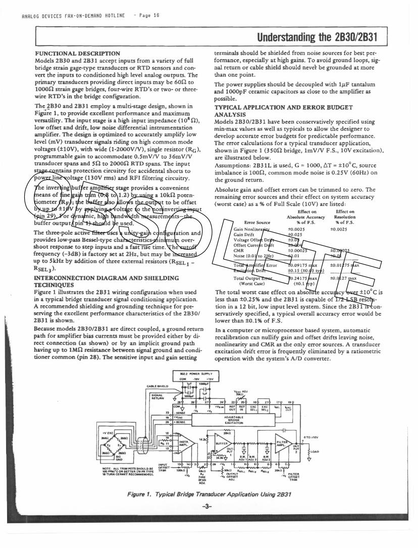
Models 2830 and 2B31 accept inputs from a variety of fullbridge strain gage-type transducers or RTD sensors and con-vert the inputs to conditioned high level analog outputS. Theprimary transducers providing direct inputs may be 60S]. to1000!2 strain gage bridges, four-wire RTD's or two- or three-wire RTD's in the bridge configuration.
The 2830 and 2831 employ a multi-stage design, shown inFigU~ I, to provide excellent performance and maximumversatility. The input stage is a high input impedance (1080).low offset and drift, low noise differential instrUmentationamplifier. The design is optimized to accurately amplify lowlevel (mV) transducer signals riding on high common modevoltages (::I:IOV),with wide (l-2OO0VN), single resistor (KG).programmable gain to accommodate: O.SmVN to 36mVNtransducer spans and S!2 to 2000!2 RTD spans. The inputsrage contains protection circuitry for accidental shorts topower line voltage (130V rms) and RFI filtering circuitry.
The inverting buffer amplifier srage provides a convenientmeans of fine gain trim (0.8 to 1.2) by using a 10k!2 poten-tiometer (RF); the buffer also allows the output to be offsetby up to :tl0V by applying a voltage to the noninvertinginput(pin 29). For dynamic, high bandwidth measurementS-thebuffer output (pin 1) should be used.
The three-pole active ftlter uses a unity-gain confIgUration andprovides low-pass Bessel-type characteristics-minimum over-shoot response to step inputs and a fast rise time. The cutofffrequency (-3dB) is factory set at 2Hz, but may be increasedup to 5kHz by addition of three external resistors (RSEL1 -RSEL3)'INTERCONNECTION DIAGRAM AND SHIELDINGTECHNIQUESFigure 1 illustrates the 2B31 wiring configUration when usedin a typical bridge transducer signal conditioning application.A recommended shielding and grounding technique for pre-serving the excellent performance characteristics of the 2B3012B31 is shown. .
Because models 2B30/2B31 are direct coupled, a ground rerumpath for amplifier bias currents must be provided either by di.rect connection (as shown) or by an implicit ground pathhaving up to IM!2 resistance between signal ground and condi.tioner common (pin 28). The sensitive input and gain setting
CAIII.! SH'ELD
SlONAI.AEYU_N
termin1l1sshould be shielded from noise sources for best per-formance, especially at high gains. To avoid ground loops, sig-nal rerurn or cable shield should nevel- be grounded at morethan one point.
The power supplies should be dccoupled with IJtF tantalumand looOpF ceramic capacitors as close to the amplifier aspossible.TYPICAL APPUCATION AND ERROR BUDGETANALYSISModels 2830/2831 have been conservatively specified usingmin-max: values as well as typicals to allow the designer todevelop accurate error budgets for predictable performance.The error calculations for a typical transducer application,shown in Figure 1 (3S0!2 bridge, ImVIV F.S., 10Vexcitation),are illustrated below.
Assumptions: 2B31L is used, G '" 1000. AT '" tlOOC, sourceimbalance is 1000, common mode noise is 0.25V (60Hz) onthe ground rerum.
Absolute gain apd offset errors can be trimmed to zero. Theremaining error sources and their effect on system accuracy(worst case) as a % of Full Scale (lOV) are listed:
Effect on Effect on
Absolute Accuracy Raoludon'!bofF.S. "'ofP.S.
:1:0.0025 ~0.002S:1:0.025:to.05:1:0.004:1:0.00025:1:0.01
Enor Source
Gain NonlinearityGain DriftVoltage Offset DriftOffset CUrrent DriftCMRNoise (0.01 to 2Hz)
:1:0.00025:1:0.01
Total Amplifier ErrorExcitation Drift
:I:O.O9175max :to.01275max:to.lS (:to.03 typ)
Total Output Enor :1:0.24175max(Worst Case) (:to.1 typ)
The total worst case effect on absolute accuracy over ::I:I0oCisless than :1:0.25%and the 2B31 is capable of 1/2 LSB resolu-tion in a 12 bit, low input level system. Since the 2B31 is con-servatively specified, a typical overall accuracy error would belower than ::1:0.1%of F.S.
In a computer or microprocessor based system, automaticrecalibration can nullify gain and offset drifts leaving noise.nonlinearity and CMR as the only error sources. A transducerexcitation drift error is frequently eliminated by a ratiometricoperation with the system's AID .converter.
:1:0.0127 max
Figure 7. Typical Bridge Transducer Application Using 2831
-3-
OBSOLETE

ANALOGDEVICES fAX-ON-DEMAND HOTLINE - Page 17
283012831BRIDGE EXCITATION (2BH)The bridge excitation stage of the model 2831 is an adjustableoutput. shon circuitprou:ctcd, regulated supply with internally.provided reference voltage (+7.ISV). The remote sensinginputs are used in the voltage outpUt mode to compensatefor the voltage drop variations in long leads to the transducer.The regulator circuitry input (pin 24) may be connected to+Vs or some oth~r positive dc voltage (pin 28 referenced)within specified voltage level and load current range. User-programmable constant voltage or constant current excitationmode may be used. Specifications are listed below in Table 1.
MODEL 283)J 2831)( lBULCoostant Vol- Output Mo.
RelJUlator Input Volt.,e ~ ..9.5V to <l8VOutputVoltlgcR...,.. +-4Vto+15VRepiator Input/Output Vol-
Diffm:ntialOutput Cu""nt'Rqulatioo, OutpUt Volt..,
¥s. SupplyLoad RCJULat.ion.It. ~ ImA to
1t..50mAOutput Vol..,., n. Temperature
(0 to +10'C)Output No;'"Reference Vol- (Inrcmal)
Connant Currrnt Output ModeReplalor Input Vol",&" It...,..Output Cu""nt Rang<:Compliance VoltageLoad RCJUlAcionTempera",... Coefficient
(0 to +10.C)OutpUI Noise:
3V to 2.4V0 to 1O0mA max
0.O5~N
O.I~o.oI5%fC IIW<O.OOJ"'oC ryplmVrms1.UV:tJ"
+95V to +2.8VlOOl<Ato lOrn...0 to 10V0.1"
0.003VCIjiArms
""'1pUI c""".. Ocr to UmA mu for 14V Japull""'l"'t~dllf_DtioI.
Table I. Bridge Excitation SpecificationsOPERATING INSTRUCTIONS
Gain Setting: The differential gain. G, is detennined accordingto the equation:
G =(1 +94kil/Rc) (20kO/(RF + 16.2kO)]
where Rc is the input stage resistor shown in Figure 1 and RFis the variable IOkO resistor in the output stage. For bestperfonnance, the input stage gain should be made as large aspossible, using a low temperatUre coefficient (1 Oppmt C) RG I
and the output stage gain can then be used to make a :t20%linear gain adjustment by varying Rp.
Input Offset Adjustment: To null input offset voltage. an op'tionaiiOOkil potentiometer connected betWeen pins 13 and14 (Figure I) can be used. With gain set at the desired value,connect both inputs (pins 12 and 15) to the system common(pin 28). and adjust the IOOkO potentiometer for zero voltsat pin 3. The purpose of this adjustment is to null the internalamplifier offset and it is not intended to compensate for thetransducer bridge unbalance.
Output Offset Adjusnnentl The output of the 2830/2831 canbe intentionally offset from zero over the :i:10V range by apply-ing a voltage to pin 29. e.g., by using an external potentiometeror a fixed resistor. Pin 29 is nonnally grounded if output off.setting is not desired. The optional filter amplifier offset nullcapability is also provided as illustrated in Figure 1.
Filter Cutoff Frequency Programming: The low pass filter cut-off frequency may be increased from the internally set 2Hz bythe addition of three external resistors connected as shown in
Figure I. The values of resistors required for a desired cutofffrequency. fe>above 5Hz arc obtained by the equation below:
RSELl= 11.6 X IO6/(2.67fc - 4.34);
RSELZ = 27.6 X 1O6/(4.12fc - 7)
RSEL3 =1.0S X 106/(O.806fc -1.3)
where RSEL is in ohms and fc in Hz. Table II gives the nearest1% RSEL for several common filter cutoff (-3dB) frequencies.
RSELl (~m RSEU (leU) RSELI (W)fc (Hz) (Pin) to ~) (Pin 9 '" 8) (Pin 8 106)
\Z Open Open Open5 1210.000 2.050.00 38J.00010 523.000 806.00 154.00050 90.000 U7.00 26.100100 #.200 68.10 lUOO500 8.660 B.~O 2..6101000 4.320 6.65 1.3005000 0.866 1.33 0.2.61
Table II. Filttlf' Cutoff Frequency vs. RSEL
Voltage Excitation Programming: Pin connections for a con-Stant voltage output operation are shown in Figure 2. The
bridge excitation voltage, V~c, is adjusted betWeen +4V to+15V by the 20kO (SOppml C) RYSEL potentiometer. Forratiometric operation. the bridge excitation can be adjustedby applying an external positive reference to pin 25 of the2B31. The output voltage is given by: VEXCOUT =3.265VREFIN. The remote sensing leads should be externally connectedto the excitation leads at the transducer or jumpered as shownin Figure 2 if sensing is not required.
"'.,,"'.. :.~" o""", '>T'I"~. TO"""
, TO"'.'
zo,...-IH'OHI
ou,'"' 2BJ1." ...-
'LOWIzo.--,v.", "",,"'.
.m.aT"."""""' '."""""',v,-".""" '~".f,'~""'~~'~>R~\.'~::'-'T..~f"""'.."'"
Figure 2. Constant Voltage Excitation Connections
Current Excitation Programming: The constant current excita-tion output can be adjusted betWeen 100J,lA to 10mA by tWomethods with the 2B31. Figure 3 shows circuit contJgUrationfor a current output with the maximum voltage developedacross the sensor (compliance voltage) constrained to i-5V. Thevalue of programmi~ resistor RISEL may be calculated fromthe relationship: RXSEL = (VREG IN - V~P!N)!.IE~(: OUT.This application requires a stable power supply because anyvariation of the input supply voltage will result in a changein the excitation current output.'m-,.Uvt.""",
OUT>\Fr2831
~""".I~
R."."' !h ,.. . .'.IV TO.ay
."" "'" . ' .. ,....,,-,1.1""
Figure 3. Constant Current ExcitationConnections (VCOMPL ""0 to +5V)
A compliance voltage range of 0 to + lOV can be obtained byconnecting the 2B31 as shown in Figure 4. The 2kO potenti-ometer RISEL is adjusU:d for desired constant current excita-tion output. """0'_' R...
RTO
to 10'- ,. ",",0",OUTPUT
D. .......
"'-
Figure 4. Constant Current ExcitationConnections (VCO\I'L'" 0 to +10V)
-4-
OBSOLETE
ANALOG DEVICES fAX-ON-DE"AND HOTLINE - Page 18
Applyingthe 2830/2831APPLICATIONS
Strain Measurement: The 2830 is shown in Figure 5 in a strainmeasurement system. A single active gage (120n, GF = 2) isused in a bridge configuration to detect small changes in gagetesistance caused by strain. The temperatUre compensation isprovided by an equivalent dummy gage and two high precision12On resistors complete the bridge. The 283S adjuStablepower supply is set to a low +3V excitation voltage to avoidtheSelf-heating error effects of the gage and bridge elements.System calibration produces a IV output for an input of 1000microStrains. The [dter cutoff frequency is set at IOOHz.
Figure 5. Interfacing Half-Bridge Strain Gage Circuit
Pressure Transducer Interface: A strain gage type pressure:transducer (8LH Electronics, DHF Series) is interfaced by the2B31 in Figure: 6. The 2831 supplies regulated excitation(+10V) to the transducer and operates at a gain of 333.3 toachieve 0-10V output for 0-10,000 p.s.i. at the pressure trans-ducer. Bridge Balance potentiometer is used to cancel out anyoffset which may be present and the Fine Span potentiometeradjustment accurately sets the full scale output. Depressingthe calibration check pushbutton switch shunts a system cali-bration resistor (ReAL) across the transducer bridge to give aninstant check on system calibration.
.""
2B35""""'.upp\.v
2B3O
"LTE.U,.AOI.
.....an ...,on 'Uk"
COOt -111'1 .-
::-E.~J~~E.....
c.o.L,,"0:;.
Figure 6. Pf'e$$UreTransducer Interface App/iCiltion
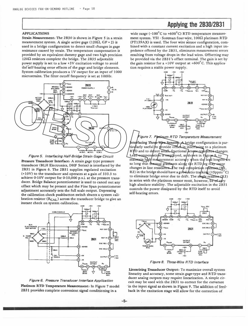
Platinum RTD Temperature Measurement: In Figure 7 model2B31 provides complete convenient signal conditioning in a
wide: range (-100°C to +600oC) RTD temperature measure-ment system. YSI - Sostman four-wire, lOOn platinum RTD(PT139AX) is used. The four wire sensor configuration, com-bined with a constant current excitation and a high input im-pedance offe:red by the 2831, eliminates measurement errorsresulting from voltage drops in the lead wires. Offsetting maybe provided via the 2831's offset terminal. The gain is set bythe gain resistor for a +lOV output at +600°C. This applica-tion requires a stable power supply.
COM -IIY .IIY
."""".
-I5Y
Figure 7. Platinum RTD Temperature Measurement
Interfacing Three-Wire Sensors: A bridge configuration is par-ticularly useful to provide: offset in interfacing to a platinumRTD and to detect small, fractional sensor resistance changes-Lead compensation is employed, as shown in Figure 8, tomaintain high measurement accuracy when the lead lengths areso long that thennal gradientS along the RTD leg may causechanges in line resistance. The two completion resistors (Rl,R2) in the bridge should have agood ratio tracking (:f:Sppm/oC)to eliminate bridge error due to drift. The single resistOr (R3)in series with the platinum sensor must, however, be of veryhigh absolute: stability. The: adjustable excitation in the 2831controls the power dissipated by the RTD itself to avoidself-heating errors.
COM ',SY-ISV
'-II""",,'
oto+-
FigureB. Three-WireRTD Interface
llneariUng :rraosducer Output: To maximize overall systemlinearity and accuracy, some strain gage-type and RTD trans-ducer analog outputs may require linearization. "A simple cir-cuit may be used with the 2831 to conect for the curvatUre
'in the input signal as shown in Figure 9. The addition of fced-back in the excitation stage will allow for the correction of
-5-
OBSOLETE

ANALOGDEVICES FAX-ON-DEMANDHOTLINE - Page 19
2830/2831nonlinearity by the addition of two components. The senseof the feedback is determined by whether the nonlinearityis concave upward or concave downward (jumper A to pin 21,or to pin 25). The magnitUde of the correction is detenninedby the resistor, RSEL' and the linearity adjust pot providesa fine trim.
If an RTD is to b;c:used, the adjustment can be made effi-ciently, without actUally changing the temperatUre, bysimulating the RTD with a precision resistance decade. Theoffset iSluijusted at the low end of the resistance range, thefine span is adjusted at about one third of the range, andthe linearity is adjusted at a resistance c;orresponding tofuU~a1e temperatUre. One or two iterations of the adjUSt-ments will probably be found necessary because of theinteraction of linearity error and scale..factor error. Thiscircuit's applications are not restricted to RTD's; it willwork in most cases where bridges are used - e.g.,loadcellsand pressure transducers.
""" -- ....
DVII'U'DIO..",
~.."-. .........,
HOT"1.""'0' - YO """ OV<NOINGOH""""".o,tv "",""ON..'.-TOPI.""oo,... u:" """""""'1Y0' PO",'.- TO'..., , "',~~:=~,W:A~=,~~:r",=::~:::'r"-"",,.~
Figure 9. Transducer Nonlinearity Correction
PERFORMANCE CHARACTERISTICSInput Offset Voltage Drift: Models 2B30/2B31 are availablein three drift selections: :to.S.:t:l and :t:3IlV/oC (max, RTI, G =1000V/V). Total input drift is composed of two sources (input:and output stage drifts) and is gain dependent. Figure 10 is a.graph of the worst case total voltage offset drift vs. gain forall versions.
0.1 .Figure 10. Tots/Input OffSlttDrift (Worst esse) vs. Gain
Gain Nonlinearity and Noise, Nonlinearity is specified as a per-cent of fun scale (IOV). e.g. 0.2SmV RTO for 0.0025%. Threemaximum nonlinearity selections offered are: :t:0.0025%,:to.OOS%and :1:0.01%(G "" 1 to 2000VN). Models 2B30/2831
offer also an excellent voltage noise performance by guaran-teeing maximum RTI noise of IIlV Pop (G = lOOOVN, Rs '"SkU) with noise bandwidth reduced to 2Hz by the LPF.
\
Common Mode Rejection: CMR is rated at :tIOV CMV andIkil source imbalance. The CMR improves with increasinggain. As a function of frequency, the CMR performance is en-hanced by the incorporation of low pass filtering, adding tothe 90dB minimum rejection ratio of the insrrumenta.tiOf) am-plifier. The effective CMR at 60Hz at the output of the filter(fc ""2Hz) is 140dB min. Figure 11 illustrates a typical CMRvs. Frequency and Gain.
110
,..
,...'I,IS~ '".::!
~ ,..~~ ..
10
.., , ,.
Figure 1,. Common-Mode Rejection "s. Frequency and Gain
Low Pass Filter, The three pole Bessel-type active filter attenu-ates unwanted high-frequency components of the input sig-nal above its cutoff frequency (-3dB) with 6OdB/decade roll-off. With a 2Hz filter, attenuation of 70dB at 60Hz is obtained,settling time is 60Oms to 0.1% offinal value with less than 1%overshoot response to step inputs. Figure 12 shows the filterresponse.
...CC . ,. '. '" >6INFUT-<>U11'UTIIOI..TAG£OIF".""Al- V
n.
-1.
,....
-20 10
f '"Ii 10! 00
~ ..~ ..
II-i-~ ...
-to-10
...
10
C,I . toF~'OU'NCY- ...
.00
Figure 12. Filter AmplitudeResponse vB.Frequency
Figure 13. Maximum LoadCurrent VB.Regu/ator Input-Output Voltage Differential
Bridge Excitation (2B31): The adjustable bridge excitation isspecified to operate over a wide regulator input voltage range(+9.5V to +28V). However. the maximum load current is afunction of the regulator circuit input-output differential volt-age. as shown in figure 13. Voltage output is short circuitprotected and itS temperatUre coefficient is :to.01S% VOUT/oCmax (:t:0.OO3%/'C typ). Outputtemperature stability is directlydependent on a temperature coefficient of a reference and forhigher stability requirements, a precision external referencemay be used.
+
~-
I II I.... t...L
,! \.
i i
. ! I \, I1--",j II f
OBSOLETE