689 ' # '5& *#6 & 7 - opencdn.intechopen.com/pdfs-wm/37192.pdf · implantation...
TRANSCRIPT

3,350+OPEN ACCESS BOOKS
108,000+INTERNATIONAL
AUTHORS AND EDITORS114+ MILLION
DOWNLOADS
BOOKSDELIVERED TO
151 COUNTRIES
AUTHORS AMONG
TOP 1%MOST CITED SCIENTIST
12.2%AUTHORS AND EDITORS
FROM TOP 500 UNIVERSITIES
Selection of our books indexed in theBook Citation Index in Web of Science™
Core Collection (BKCI)
Chapter from the book Ion ImplantationDownloaded from: http://www.intechopen.com/books/ion-implantation
PUBLISHED BY
World's largest Science,Technology & Medicine
Open Access book publisher
Interested in publishing with IntechOpen?Contact us at [email protected]

10
Neon and Manganese Ion Implantation into AlInN
Abdul Majid Department of Physics, University of Gujrat
Pakistan
1. Introduction
This chapter deals with the experimental study of ion implantation into wurtzite AlInN, grown by metal organic chemical vapor deposition (MOCVD) technique. III-nitride alloys (AlGaN, InGaN and AlInN) are the materials which provide tunable energy band gap, effective mass of the carriers, lattice and dielectric constants depending upon the alloy composition. Unlike AlGaN and InGaN, little attention has been paid to the study of AlInN because of the growth related problems. The first ever AlInN layer in the form of polycrystalline film was grown and reported by Starosta in 1981 when he fabricated such layers by means of radio-frequency (RF) reactive multi-target sputtering [1]. Later, Kubota et al reported high quality growth of Al1−xInxN layers by RF magnetron sputtering in 1989 and demonstrated the compositional dependence of band gap and lattice constant in the whole composition range x = 0 to 1 [2]. Following these earliest efforts, many groups engaged themselves for the growth and characterization of AlInN layers [3, 4].
AlInN is a potential direct wide band gap compound semiconductor material for high power, high frequency and high temperature applications in electronic and optoelectronic devices due to its exceptional physical and chemical properties [5, 6]. The property which makes III-V nitrides prominent over the other compound semiconductors is the availability of wide band gap range from 0.7 eV (InN) to 6.2 eV (AlN), covering emission wavelengths from infrared (IR) to UV [7]. AlInN is the only III-nitride alloy which has ability to be grown perfectly lattice matched to GaN for indium content of 17-18 % [2]. In lattice matched composition, AlInN has larger band gap and higher refractive index with respect to GaN which makes this alloy attractive for several photonic applications [8, 9].
The fabrication of many of the devices mentioned above requires efficient, controlled and selective area doping. Although doping during the growth of materials can be performed but doping by ion-implantation offers several advantages, which can not be achieved by in-situ doping of III-nitrides. The low solubility of transition metal ions into III-V semiconductors (>1018cm-3) has put limits on their doping for achieving variety of magnetic semiconductor materials. Fortunately, ion implantation equipped with several added advantages has potential to act as an alternate technique [10]. Incorporation of any dopant atom at any desired depth of material with known concentration above solid solubility limits and selective area doping are advantages of doping by ion-implantation [6]. Furthermore it offers additional processing benefits like, electrical isolation, dry etching, quantum well intermixing and ion cut etc. Along with several unique benefits of ion
www.intechopen.com

Ion Implantation
204
implantation there are disadvantages like lattice damages and production of new defects [11]. A well established remedy to remove the implantation induced damages is the thermal annealing of the samples. The optical, electrical and magnetic activation of dopants is also achieved by the thermal annealing. There are several parameters that have to be taken into account for successful optimization of annealing to recover the lattice, e.g. annealing time, annealing temperature, annealing atmospheres, sample thickness, cap layers and implantation parameters.
In order to enhance the functionality of devices, scientists have shown a great enthusiasm to exploit the spin of electrons [12]. The communication between microelectronic devices occurs by the flow of charges; however the movement of spin can also be used to carry information among devices [13]. This has opened the possibility to utilize the charge and spin degrees of freedom simultaneously, to realize a new generation of electronic devices known as spin-electronic or spintronics [14]. The diluted magnetic semiconductors (DMS) are a class of materials in which small quantity of magnetic ions is introduced into normal semiconductors, are found suitable for spintronic device applications [15]. The most investigated DMS are (GaMn)As and (InMn)As but these suffer from the limitation of Curie temperature and disqualify for use in the practical spintronic devices [16, 17]. Dietl in year 2000 have predicted the possibility of Curie temperature above room temperature in GaN based DMS and provided new basis for DMS research [18]. Extremely high Curie temperature of around 940 K has been reported in 2002 for wurtzite GaN doped with Mn [19]. Unlike other nitride alloys, only few reports are available in the literature, on ion implantation into AlInN [20, 21]. The production and variation of residual strain caused by ion implantation in semiconductor crystals has been observed [22]. Lorenz et al have reported that the strain state of AlxIn1-xN/GaN switches from tensile to the compressive when T shifts from negative to positive on increasing the indium content beyond 17% [23, 24] have reported the electrical isolation of implanted AlInN but no report is available on the other areas like doping, microstructural changes and defect studies in this implanted material.
2. Background
2.1 Group III-Nitride semiconductors
Group III-Nitride semiconductors are the compounds of metals from group-III with nitrogen (group-V) which offer the binaries GaN, InN, AlN ternaries AlInN, AlGaN, InGaN and quaternary AlInGaN. The strong polarity of III-N bond makes these materials chemically stable and physically tolerant for the devices to work at high temperature, high frequency and in hostile environment [25]. These materials have earned the extensive research and industrial interest due to their promising technological capabilities for the electronic and opto-electronic devices [26]. Current applications of III-nitrides include ultraviolet/visible laser diodes, ultra-bright LEDs, UV detectors, high temperature electronics, high-density optical data storage, aerospace and automobiles technologies [6]. A variety of growth techniques have been used to achieve III-nitrides since 1862 when AlN powder was first made [27].
The choice of a lattice matched and thermally compatible substrate is a critical requirement for the homoepitaxial growth of semiconductors. Unfortunately, no such substrates are
www.intechopen.com

Neon and Manganese Ion Implantation into AlInN
205
available for III-nitrides which have made heteroepitaxial growth, a practical necessity that puts limits on the quality of these materials. Along with the lattice and thermal compatibility, substrate should have some other qualities like, reasonably flat surface with minimum size of two inch diameter and ability to withstand high concentration of ammonia and hydrogen at elevated temperatures. Many substrate materials like Si, NaCl, GaP, InP, W, ZnO, MgAl2O4, TiO2, MgO, SiC, Al2O3 etc have been tested for the heteroepitaxial growth of III-nitride [5]. However, sapphire and silicon carbide are the most popular materials for III-nitride heteroepitaxy on the basis of the pre-suppositions mentioned above.
III-nitrides can be crystallized into wurtzite, zincblende and rocksalt structures. However, under ambient growth conditions, wurtzite is the thermodynamically stable crystalline structure for these materials. The wurtzite structure has hexagonal unit cell containing 6 atoms of each type, with in-plane and out-of-plane lattice parameters ‘a’ and ‘c’ respectively. The space group of wurtzite structure is P63mc ( 4
6vC ). The wurtzite crystal structure consists of two interpenetrating hexagonal closed pack sub-lattices, off-set along c-axis by 5/8 of the cell height. Each group-III atom is coordinated by four nitrogen atoms in tetrahedral arrangement.
2.2 Aluminum indium nitride (AlInN)
Aoming III-nitride alloys AlGaN, InGaN and AlInN, little attention has been paid to the study of AlInN because of the growth related problems. AlInN layers suffer crack formation and phase segregation due to large mismatch between InN and AlN. Following these earliest efforts [1, 2] many groups engaged themselves for the growth and characterization of AlInN layers [3, 28] A schematic structural sketch of AlInN is shown in figure 1.
Fig. 1. Crystalline structure of AlInN (a) pure (b) Mn doped
The energy band gap of AlInN can be tuned at any value between the band gaps of InN (0.63 eV) [ref. 29] and AlN (6.2 eV) [ref. 30] which makes the material a promising candidate for several electronic and optoelectronic applications. Owing to the unique qualities, AlInN based structures are expected suitable for AlInN/GaN superlattice that can be used for applications in near IR devices based on inter-sub-band transitions [31], distributed Bragg
www.intechopen.com

Ion Implantation
206
reflectors (DBRs) [8], high quality factor microcavities [32] and high electron mobility transistors (HEMTs) [31]. The composition ‘x’ of Al1−xInxN alloy is usually found from a linear interpolation between the relaxed bulk lattice constants of pure AlN (a=3.112 Å, c=4.982 Å) and InN (a=3.548 Å, c=5.760 Å) by assuming a linear relationship between the ternary composition and its lattice parameters. This method is known as Vegard’s law [33]. However, it is suggested to use the Vegard’s law carefully due to the phenomenon of band gap bowing, which gives the alloy composition lower than that calculated from Vegard’s law [34]. The wurtzite Al1−xInxN is a material having direct energy gap Eg of 0.7 <Eg< 6.2 eV at 300 K [29]. The lattice parameters ‘a’ and ‘c’ lie in the range 3.112 <a< 3.548 Å and 4.982 < c< 5.760 Å respectively. The band gap and lattice parameters can be tuned by changing the indium mole fraction ‘x’ in the alloy. The band gap bowing phenomenon observed due to the deviation from Vegard’s law is usually quantified by a bowing parameter ‘b’ which can be estimated by using the relation [35].
, ,( ) (1 ) (1 )g g InN g AlNE eV xE x E bx x
High resolution X-ray diffraction has been proved to be successful in strain measurements of epitaxial films [36, 37]. The ‘a’ and ‘c’ lattice constants are usually found from skew-symmetric and symmetric XRD reflections respectively. Both the biaxial in-plane and out-of-
plane strain can be determined by using the relations o
o
a a
a and o
o
c c
c
respectively, where ao and co are the respective in-plane and out-of-plane lattice constants of unstrained relaxed bulk material [38].
2.3 Ion implantation into III-nitrides
Ion implantation into semiconductors offers a multipurpose processing tool used for the selective area doping, electrical isolation, dry etching, quantum well intermixing and ion cut etc [39]. William Shockley was the first who introduced ion implantation for doping of desired atoms into semiconductor materials. He got his technique registered as a patent in 1954 and later first commercial Ion-implanter was launched to the market during 1970s. Figure 2 highlights the suitable elements in the periodic table for implantation into semiconductors [10].
2.4 Ion implantation into AlInN
Unlike other nitride alloys, AlInN has not gain a considerable research interest from the implantation point of view, possibly due to its poor crystalline quality. The change in strain caused by the implantation and thus variation of the tetragonal distortion ( T ) provides valuable information about the structural properties of implanted material. The production and variation of residual strain caused by ion implantation in semiconductor crystals has already been observed [22]. Lorenz et al have reported that the strain state of AlxIn1-xN/GaN switches from tensile to the compressive when T shifts from negative to positive on increasing the indium content beyond 17% [23]. Pearton et al [24] have reported the electrical isolation of implanted AlInN but no report is available on the other areas like doping, microstructural changes and defect studies in implanted material.
www.intechopen.com

Neon and Manganese Ion Implantation into AlInN
207
Fig. 2. Elements of periodic table used for ion implantation [10]
Despite promising benefits of ion implantation, this technique is still far away from its applications in GaN based devices. Prior to the use of implantation for a certain purpose, one has to optimize the implantation and thermal annealing conditions. Besides this, the implantation of different ions has shown different effects on different materials, therefore detailed investigations of implantation effects on AlInN are needed to explore the possibilities of the expected advantages.
A technologically well known phenomenon is the impurity gettering which has become a mature technique for silicon industry to getter the unwanted transition metal impurities. It is well known that inert gases produce cavities or bubbles in solids which contain high density of dangling bonds that exhibit high affinity for metallic contaminants to act as gettering centers. The formation of inert gas cavities in GaAs, SiC, InP etc urged us to implant the neon ions into AlInN which is still lacking in literature.
Until now, appropriate annealing conditions have not been established for the treatment of the implanted AlInN; therefore, different researchers have reported different results for same material and implantation conditions. The magnetic properties of the implanted semiconductors strongly depend upon annealing conditions. Manganese is the mostly used magnetic impurity in semiconductors to realize the DMS. Although few report are available for ion implantation into AlInN but no one has focused the study of effects of annealing on its properties. Therefore, a lot of work is still needed to optimize the annealing parameters for ion implanted AlInN.
Many groups have reported ferromagnetism in GaN, InN, AlN and related alloys AlGaN and InGaN by incorporating magnetic ions but there is no report on AlInN based DMS. To realize all possible benefits of nitride based DMS, ferromagnetic properties of all III-Nitride members should be known. AlInN is expected to be a promising DMS material after doping
www.intechopen.com
Ion Implantation
208
of magnetic ions and possibly the future magnetic DBR for polarization stability in the spin VCSELs. This has motivated us to implant magnetic ions into AlInN to fabricate the room temperature DMS based on AlInN.
3. Experimental details
This section describes the fabrication/processing of the samples and the characterization techniques used during this study. First section of this chapter deals with the fabrication of samples which consists of epitaxial growth by using metal organic chemical vapor deposition (MOCVD) along with the post fabrication processing which comprises high energy ion implantation and thermal annealing. After fabrication, the samples were studied in detail by means of the structural, optical, electronic and magnetic characterizations with variety of techniques described in the second section of this chapter.
The preparation of the samples comprises three major steps; fabrication using MOCVD technique, implantation of energetic ions into the grown materials and thermal annealing of implanted samples.
3.1 MOCVD growth of samples
All the samples used in this study are grown in a low pressure MOCVD system. Some times this technique is also referred as Metal Organic Vapor Phase Epitaxy (MOVPE) or Organo Metallic Vapor Phase Epitaxy (OMVPE). During the fabrication of the samples, a mixture of gases (called precursor) containing the materials required for deposition of the sample is passed over the heated substrate. The chemical decomposition (Pyrolysis) of precursor gases takes place in high temperature chamber and the atoms (needed for deposition) then deposit onto the substrate thereby making the bonding to build a crystalline layer. The growth process is sketched below in figure 3.
MOCVD growth has several advantages over other growth techniques (e.g. MBE). The growth process in MBE is controlled only by substrate temperature and molecular flow rates, whereas, MOCVD offers a variety of parameters (chamber pressure, gas flow and wide range of precursors) which make it more versatile. The precursors consist of organic materials which are less toxic, liquid at room temperature and inexpensive for industrial mass production. Moreover, no ultrahigh vacuum is needed like in MBE.
Samples were grown in a horizontal MOCVD reactor manufactured by Thomas Swan Scientific Equipment Limited. Hydrogen was used as a carrier gas for the growth of the samples. The c-plane sapphire wafers (Al2O3) of 2 inch diameter ware used as substrates for growth of the materials. The samples used during this study were hexagonal thin films of GaN and AlInN fabricated in the form of GaN/sapphire and AlInN/GaN/sapphire respectively. During the fabrication of GaN, the first step was the growth of a low temperature thin GaN buffer layer on a sapphire substrate. Next step was the growth of a GaN epilayer without any doping (so called i-GaN) i.e. GaN template. In case of doped samples, silicon and magnesium were incorporated to produce n- and p-GaN respectively. Sketches of AlInN samples used in this study are given in figure 4. For the fabrication of AlInN samples the first step was the growth of GaN template as described earlier. After that AlInN epilayer was grown without any doping. The samples were then classified into two groups. One group was left as it is, for further processing whereas other group of the AlInN samples was capped with GaN cap-layer as shown in fig. 4 (b).
www.intechopen.com

Neon and Manganese Ion Implantation into AlInN
209
Fig. 3. Schematic diagram of MOCVD growth process.
Fig. 4. Layered sketches of the AlInN samples used in this study.
Precursors for the MOCVD growth of III-nitrides consist of organic compounds involving elements from groups III and V along with a dopant precursor (if needed). A list of precursors used for growth of different samples is given below in table 1.
The samples with best structural and electrical properties were grown after the optimization of growth parameters. The growth conditions involve the chamber temperature, chamber pressure, precursors, precursor’s flow rates, substrate rotation rate and growth time etc. Growth conditions of the samples used in this study are given in table 2.
Hall and X-Ray diffraction measurements were carried out to select the high quality wafers for further study. The samples of 1x1 cm2 size were then carefully scribed from wafers to
www.intechopen.com

Ion Implantation
210
obtain different sets of samples and each set of samples scribed from the same wafer was used separately for implantation of different ions. The scheme of ion implantation is given in the next section.
Precursor Chemical symbol Advantages Disadvantages TMGa Tri-methyl gallium (Group III-Precursor)
(CH3)3Ga liquid, high vapor pressure
Volatile and dangerous for contact to human body
TMIn Tri-methyl indium (Group III-Precursor)
(CH3)3In solid, good vapor pressure for MOCVD
low vapor pressure
TMAl Tri-methyl aluminum (Group III-Precursor)
(CH3)3Al liquid, good vapor pressure, good long term stability
oxygen contamination
Ammonia (Group V-Precursor)
NH3 good stability, only practically available nitrogen precursor
high Pyrolysis temperature
Silane (n-dopant)
SiH4 used as n-dopant for electronic devices
gaseous, flammable, high Pyrolysis temperature
Cp2Mg Bis- (cyclopentadienyl) magnesium (p-dopant)
(C5H5)2Mg used as p-dopant and has low volatility
Volatile and dangerous for contact to human body
Table 1. List of precursors used for growth of samples.
No. Sample and Purpose
Growth steps
Time (sec)
Temperature(oC)
Pressure(Torr)
NH3 (ccm)
TMGa (ccm)
SiH4 (ccm)
cp2Mg (ccm)
TMIn (ccm)
TMAl (ccm)
1 AlInN (Used for Mn implantation)
1.GaN 850 1040 200 3500 51 0.05 ---- ---- ---- 2.AlInN 5900 820 100 5200 N.A N.A N.A 200 20
2 AlInN (Used for Ce implantation)
1.GaN 850 1040 200 3500 51 0.05 2.AlInN 3550 820 60 5500 ---- ---- ---- 410 20 3.GaN
cap-layer180 800 200 3000 30 ---- ---- ---- ----
3 AlInN (Used for Ne Implantation)
1.GaN 850 1040 200 3500 51 0.05 ---- ---- ---- 2.AlInN 5200 820 90 4000 N.A N.A N.A 470 20 3.GaN
cap-layer180 800 200 3000 30 ---- ---- ---- ----
Table 2. Growth conditions of AlInN samples used in this study.
3.2 Ion implantation
Ion implantation is a process in which impurity ions are projected into the target material to modify its structural, optical and electronic properties. It is relatively a simpler technique for
www.intechopen.com

Neon and Manganese Ion Implantation into AlInN
211
introducing the ions into a semiconductor for doping, electrical isolation of active regions and device applications. Some of the several advantages of doping by ion implantation over the doping during growth are listed below.
1. It is an inexpensive and quick method to achieve the required material. 2. Any species of ion can be incorporated into any host material. 3. Ion can be introduced at the desired depth by the control of implantation energy. 4. Ions can be implanted into the desired areas of the sample for the selective area doping
by the use of a proper mask system. 5. The required concentration of the ions can be implanted into the material after
monitoring the implantation dose which is measured by the ion current. 6. Dopants can be incorporated above the solid solubility limits. 7. It is insensitive to the host properties, i.e. sample geometry, lattice structure, lattice
defects etc. 8. It is a low temperature process.
The main parts of an ion implanter are the ion source, mass spectrometer, high voltage accelerators, scanning system and a target chamber. The material to be doped into the samples via implantation is filled in a cylindrical chamber in the form of gas. An electric potential of about 100 V is applied across the body of the chamber and the filament to generate electrons. The electrons emitted out of the filament of chamber ionize the gas atoms by impact ionization. The positive ions are accelerated towards the exit slit which is set at high negative potential of about 25 kV. The positive ions then enter the mass spectrometer which separates the ions of different masses and charge states to allow the desired ion species to pass through the exit slit of the spectrometer.
The ions selected by the spectrometer are accelerated by passing through the accelerating columns at high voltages. These ions are then passed through the pair of X and Y plates of a scanner system to produces a beam for uniform dose of implantation into the whole area of wafer. The scanned beam is passed through the defining aperture and then projected on to the wafer. Electrical contacts between the wafer and the metallic target holder facilitates the electron flow to neutralize the implanted ions received by the wafer. The ions received by the wafer are counted by the charge integrator which measures the time averaged swept beam current according to the relation,
0
tI
Q dtnqA
Where ‘A’ is the wafer area, ‘n’ is 1 for singly and 2 for doubly ionized atoms, and ‘I’ is the electron current integrated over total time of implantation. The wafer is biased at small positive voltage to minimize the secondary electron’s dose errors.
The energy with which the ions are accelerated towards the samples depends upon the applied electrostatic potential and is known as implantation energy. It depends upon the implanter set-up and is normally in the range, 1 to 2000 keV. The number of ions received by the target per unit area (ions/cm2) is known as dose and is found electronically by using a charge integrator.
The incident ion on striking the crystal surface loses its energy through scattering events during coulombs interactions with target atoms. By ignoring the complications of many-
www.intechopen.com

Ion Implantation
212
body interactions, the process can be best appreciated by the supposition of binary collision. The projected ion collides with a target atom, which in turn recoils and collides with other lattice atoms to start a collision cascade. The route of penetrating ion mainly consists of point defects (vacancy, interstitial, substitutional, antisite etc). The energy loss mechanism can be classified in two ways: the elastic or nuclear energy loss (coulomb interaction) and inelastic or electronic energy loss (electron-electron energy transfer, excitation and ionization phenomenon) [6].
The total distance covered by the incident ions normal to the target surface before coming to rest is called range of ions. It is usually denoted by R and is given by
0 ( )
EdE
RNS E
Where N is the atomic density, dE is the energy loss of ion and S(E) is the stopping cross-section.
The mean penetration depth of the ions below the target surface is an important parameter and is known as projected range. This is denoted by Rp and it is smaller than the actual distance R traveled by ions. The relation between R and Rp is approximated as
2
11
3
P
RR
m
m
Where m1 and m2 are the masses of incident and target atoms respectively.
The distance traveled by the ions along the normal to the incidence direction is referred as the lateral range and is denoted by R, whereas the spread in ion range caused by the fluctuations in energy loss mechanism is known as straggling range. Some ions stop at depth less than Rp and some at depth greater than Rp. Therefore, standard deviation or straggling (usually denoted by ∆Rp) is used to find the distribution around Rp. The range and distribution of implanted ions into the target have been described by Lindhard, Scharff and Schiott (LSS) theory [40], according to them the distribution of implanted ions follows Gaussian function.
The concentration of implanted ions at a certain depth x can be written as
2
2( )
2max( )
P
P
x R
RN x N e
Where Nmax is the peak concentration of implanted ions and is given by
max0.4
2 PP
NRR
Where is the ion dose in ion/cm2, using this value of Nmax we can find N(x) as,
www.intechopen.com

Neon and Manganese Ion Implantation into AlInN
213
2
2( )
2( )2
P
P
x R
R
P
N x eR
A more exact and quick way to find the range, distribution and damage analysis of implanted ions into target is the computer simulations. Transport and range of ions in matter (TRIM) is a comprehensive Monte Carlo binary collision computer simulation based on full quantum mechanical treatment of ion-atom collisions [41]. It is capable of providing the distribution of the ions as well as all kinetic phenomena associated with the ion's energy loss (target damage, sputtering, ionization, and phonon production) in the multilayered complex target materials.
Though Gaussian distribution is a reasonable approximation of the depth profile of implanted ions but this is true mostly for the amorphous targets. Due to higher crystallinity of semiconductor crystals, incident ion if implanted parallel to the crystal axis, moves through the crystal planes without facing any collision and most probably channel into the substrate. To avoid such channeling effect implantation is usually carried out in such a way that target crystal is tilted 7o off the direction of incident ions.
No. Sample name Material Implanted ion
Implantationenergy (KeV)
Implantationangle
(Degree)
Beam current
(µA)
Implantation dose
Ions/cm2
1 TH070207E
AlInN Neon 250 7 0.4 1x10¹⁴
1.8 2x10¹⁵
1.8 5x10¹⁵ 1.8 9x10¹⁵
2 TH070206C
AlInN Manganese 250 7 0.6 1x10¹⁴
5.5 2x10¹⁵
7 5x10¹⁵ 10 9x10¹⁵ 14 2x10¹⁶ 14 5x10¹⁶
Note: Implantation is carried out at room temperature.
Table 3. Implantation conditions used for this study.
LC-4 high energy ion implanter installed at Institute of semiconductor, Chinese academy of science, Beijing, China was used for the implantation of the samples used for the work reported in this thesis. This implanter is manufactured by Institute No. 48, China Electron Science and Technology group. Implantation conditions for different samples are given in the table 3.
3.3 Thermal annealing
The energetic ion-implantation into semiconductor lattice leads to the production of defects, damages, local amorphous regions and disordered crystalline structures. In spite of the several benefits, ion implantation damages the lattice that causes quenching of the
www.intechopen.com

Ion Implantation
214
luminescence, band filling, band gap narrowing and band tailing effects. Such effects severely affect the electrical and optical properties of the devices. A necessary step after implantation of the samples is the thermal annealing, which not only recovers the lattice but also moves the implanted ions to a suitable place for the electrical, optical and magnetic activation of the dopants.
Rapid thermal annealing (RTA) is a process in which semiconductor samples are heated up to very high temperatures (up to 1000oC or even higher) for a short time (several seconds) in a controlled way. Rapid heating rates (1000oC per minute) and thus short time processing offered by RTA is its major advantage over the conventional furnace annealing (takes several hours). Moreover, RTA ensures comparatively high security, when sample decomposition is taken into account since sample is exposed to the high temperature for a very short interval of time. High temperature annealing of III-nitrides is usually performed in the nitrogen ambient to counter the loss of nitrogen from the surface of the samples. Rapid thermal annealing has been found an effective way to improve the crystal quality and repair the implantation induced damages in III-nitrides.
An RTA processor mainly consists of three major components, RTA chamber, a heating system and a temperature sensor.
RTA has been performed in an RTP-300 rapid thermal processor that uses 13 tungsten halogen lamps (1250 W each) as a heat source and a nitrogen gas flowing ambient. The temperature sensor used during RTA is K-type thermocouple embedded in the sample stage. The samples to be annealed have been placed inverted on another GaN wafer which is then put on the 4 inch silicon wafer positioned on the sliding sample holder in side the RTA chamber. After inserting the sample holder inside the chamber, window is tightly closed by the screws. RTA is programmed for the specified temperature and time.
Usually semiconductors are annealed up to the maximum temperature equal to 2/3 of the melting point of bulk martial. This suggests the use of annealing temperature of about 1800oC for GaN whose melting point is 2791oC. However, this temperature is normally higher than the growth temperature of the epitaxial semiconductors which may degrade the material due to its decomposition. Therefore, annealing temperature and time needs to be carefully optimized to keep a balance between the lattice recovery and the sample degradation. Many experiments were carried out by using the different annealing conditions for the search of optimized values of annealing time and temperature. In this study we have used the maximum annealing temperature of 1000oC for GaN and 850oC for AlInN with annealing time of 30 seconds.
3.4 Characterizations techniques
Several techniques were used for the characterization of as-grown and implanted samples to study the effects of ion implantation on the structural and magnetic properties of the materials. Following section describes the characterization techniques used for this study. Ion implantation produces modifications in the lattice of the materials which can be studied by performing the structural characterizations of the samples. In this study, X-Ray diffraction and Rutherford backscattering spectroscopy have been used for the study of the structural changes induced by the implantation and annealing of the samples.
www.intechopen.com

Neon and Manganese Ion Implantation into AlInN
215
3.4.1 X-ray diffraction
X-Ray diffraction (XRD) is very useful technique for the structural analysis of the crystalline samples. It offers an efficient way to identify the crystal structure and explore the lattice modifications in the implanted/annealed samples.
X-rays emitted out of the material as a result of inter shall transitions are used as probe for analysis in X-ray diffractometer. These rays are produced by the bombardment of high energy electrons on a copper target and then filtered to give a monochromatic beam of Cu-Kα radiation. When X-rays are incident onto a crystalline material they are diffracted from the planes of the crystal. The diffraction peak is obtained only when the distance traveled by the rays after reflection from the successive crystal planes differs by an integral multiple of wavelengths. This process takes place in accordance with the well known Bragg’s equation, given below.
2 sind n
Where d is interplaner spacing, θ is the incident angle, ┣ is the wavelength of incident X-rays and n is the order of diffraction. By changing the angle θ, the Bragg’s conditions are satisfied and a strong reflection or XRD peak is obtained. The plot of the angular positions verses the intensities of the diffracted peaks produces a pattern, which is a characteristic of the material. The position of the peaks recorded in XRD spectrogram is compared with the peaks of known materials for the phase analysis of the samples.
XRD analysis of the samples was performed using Cu-Kα source of X-rays at room temperature by Rigaku SLX-1A X-ray diffractometer. Crystallinity of GaN and AlInN samples was studied in detail by performing /2θ scans using double axis and triple axis diffraction. Furthermore, broadening of the peaks, tilt and twist features were also studied by the measurements of FWHM from -scans of high resolution XRD. Powder diffraction XRD has been carried out in 2θ range of 20 to 100o to study the phase analysis and detection of secondary phases in implanted samples.
3.4.2 Rutherford Backscattering Spectroscopy
Rutherford Backscattering Spectroscopy (RBS) is a versatile technique for finding the concentration of the atoms, thickness of the thin film, depth distribution of the atoms and the characterization of implantation induced damages in the lattice [23, 39]. RBS in angular mode also provide information about the substitution of dopants on regular sites of the lattice [42].
This technique works on the principle of Rutherford scattering. An energetic beam of helium ions (4He+) is incident on the sample and then backscattered. The collision probability of incident alpha particle with the target atoms is determined by Rutherford cross-section. The elastic collision between incident alpha particles and target atoms suggests that the ratio of energy of the particles before and after collision is equal to the ratio of the masses of both particles. The energy of the backscattered alpha particles is analyzed, which contains the information about the atoms from which alpha particles are backscattered. According to the single scattering theory, an alpha particle faces only one large angle scattering before reaching the detector. This approximation helps to convert the
www.intechopen.com

Ion Implantation
216
energy scale into the depth scale of the sample within energy resolution of the detector. Lower is the energy of the backscattered alpha particles, deeper will be the detected atoms.
RBS measurements were performed in School of Physics, Peking University, Beijing, China. An ion beam of energy 2 MeV having diameter of 1 mm was used for this study. The samples were mounted on a two axis goniometer which has ability to align the sample at any desired angle with the incident beam. Chamber has two silicon detectors, one for the detection of particles backscattered at angle near to the incident beam and other for detection of particles backscattered at glancing angle to the sample surface. Glancing detector of resolution 18 keV was set at 165o relative to incident beam direction. This detector have aperture diameter of 5 mm and placed 80 mm away from the samples. The data obtained from RBS measurements was analyzed by using SIMNRA simulation.
3.4.3 Magnetic characterizations
The implantation of magnetic ions into AlInN is expected to make them diluted magnetic semiconductors. Therefore, magnetic characterizations of the magnetic-ion-implanted samples were carried out to search the room temperature ferromagnetism. Vibrating sample magnetometer and Superconducting quantum interference device were used for this purpose.
3.4.4 Vibrating sample magnetometry
This is a conventional technique for the magnetic characterization of the samples in which magnetic moments as a function of applied magnetic field and temperature can be recorded.
To perform the measurements, sample mounted on sample holder is placed in a uniform magnetic field and set to the mechanical vibrations at a known frequency through a vibrator. The vibrations produce a change in magnetic flux of the sample which induces a voltage in the pick up coils. This induced voltage is proportional to the magnetic moment of the sample.
DMS Model 4HF Vibrating Sample Magnetometer (VSM) of ADE Technologies having detection sensitivity 10-5 emu, was used to investigate the magnetic properties of the implanted samples. Magnetic hysteresis loops were recorded at room temperature for all the implanted samples using magnetic field 12000 Oe (Oe=oersted unit) in-plane and out-of-plane applied magnetic field of to saturate the samples. It was found that an easy axis for samples is the direction when the magnetic field is applied parallel to the sample plane (in-plane).
3.4.5 Superconducting quantum interference device magnetometry
Superconducting quantum interference device (SQUID) is a resourceful tool for the magnetic characterization of the samples. It offers a sophisticated way to detect the magnetic ordering by studying temperature dependence of magnetization (MT), field dependent magnetization (MH) and other properties of the samples. SQUID has very high sensitivity (~10-9 emu) for the detection of very weak magnetic moments. SQUID works on the principle of the electron-pair wave coherence and Josephson Effect. The flow of current across two superconductors separated by an insulated layer is known as Josephson’s effect
www.intechopen.com

Neon and Manganese Ion Implantation into AlInN
217
and current flowing is known as Josephson’s current. A Josephon’s junction consists of two superconducting coils, which are separated by a very thin insulating barrier, so that electrons can pass through it. SQUID magnetometer consists of a superconducting ring containing two Josephson’s junctions in parallel, placed in magnetic field. In the presence of a magnetic field, a current starts to flow through the superconducting loop. When a ferromagnetic sample is placed between the superconductors in the presence of applied field the magnetic flux appears to change accordingly. This change of magnetic flux induces a current which changes the current circulating through the coil. The variation in the current helps to detect the magnetic moment of the material.
SQUID was used to study the MT and MH behaviors of the magnetic ions implanted samples. During MH analysis, hysteresis loops were recorded at 100 K and 300 K for implanted samples. MH loops were also recorded for un-implanted samples and this data was subtracted from that of implanted samples. For MT measurements, the sample was cooled up to 5 K without applied magnetic field. Then magnetic field of 500 Oe was applied and scan was run up to 350 K to record zero field cooled (ZFC) trace. The sample was then again cooled down to 5 K with the field of 500 Oe and magnetization was measured to get the field cooled (FC) trace. During magnetization measurements plane of sample was parallel to the applied magnetic field.
4. Neon implantation
4.1 Neon implantation into AlInN
The samples used for this study were ~200 nm thick AlInN thin films grown on a 4µm thick GaN template. AlInN films were finally capped with a very thin GaN layer to avoid the sample decomposition during high temperature annealing. The cap layer also helps to limit the penetration depth of incident ion within AlInN layer and to avoid their interaction with the buffer layer. Sketch of the samples is shown in figure 4 (b).The chamber temperatures during growth of GaN template, AlInN layer and GaN cap layer were 1040, 820 and 800oC respectively. The detailed growth parameters of these samples are given in table 2. The crystal quality and composition of the as-grown samples was checked by X-ray diffraction. FWHM value of AlxIn1-xN peak measured by X-ray diffraction was 406 arcsec indicating its high crystalline quality. Vegard presented a way to estimate the composition of ternary alloys by assuming linear relation between composition and lattice parameters [33]. The composition of AlxIn1-xN is usually found by Vegard’s law by linear interpolation between relaxed bulk lattice constants of AlN and InN. The value of indium content in AlInN layer of as-grown sample estimated using the Vegard’s law is 8.3 %.
Neon ions were implanted at 250 keV on four samples scribed from same wafer, with doses 1014, 2x10¹⁵, 5x10¹⁵ and 9x10¹⁵ ions/cm2. The samples were implanted at room temperature and incident angle of beam was set at 7o to the c-axis of samples. The implanted samples were annealed by RTA processor at 750oC for 30 sec in nitrogen ambient. Although, annealing temperature of 400oC above the growth temperature has been reported to be safe in implanted AlInN [20], but in general, annealing temperature below the growth temperature is preferred. We have annealed the neon implanted AlInN at temperature below the growth temperature.
www.intechopen.com

Ion Implantation
218
4.2 Implantation induced strain in epilayers
Neon implanted AlInN thin films were characterized by XRD before and after annealing to study the effects of implantation and annealing on the structural properties of material [69].
Figure 5 shows the (0002) XRD curves of as-grown and neon implanted AlInN/GaN samples before annealing. The peak at 2θ = 34.56o is due to the signal from the GaN buffer layer and peak appearing at 2θ = 35.51o is due to the signal coming from AlInN epilayer of as-grown samples. After implantation, it has been observed that intensity of AlInN peak decreases with increasing dose. The position of the peak shifts systematically toward the lower angle with increase in dose up to 5x1015 cm-2. In the scans measured after maximum dose 9x1015 cm-2, AlInN peak is broad and its intensity is too small to measure its exact peak location. However it seems shifted slightly towards higher angle side as compared to its position for the samples implanted with dose 5x1015 cm-2. An additional peak structure is also observed on lower angle side of GaN peak in the scans of all implanted samples. This peak structure broadens and becomes less intense with increasing dose of implantation, indicating the expansion of GaN lattice.
34.0 34.2 34.4 34.6 34.8 35.0 35.2 35.4 35.6 35.8
AlInN(0002)
as-grown
1x10¹⁴
cm-2
2x10¹⁵
cm-2
5x10¹⁵
cm-2
9x10¹⁵
cm-2
2 (degrees)
GaN(0002)
Inte
nsity (
a.u
.)
Fig. 5. X-Ray diffraction spectra showing (0002) peaks of GaN and AlInN for as-grown and neon implanted AlInN/GaN samples before annealing. AlInN peaks are shown Lorentz fitted.
Figure 6 shows the XRD spectra of same samples after annealing at 750oC. The post annealing spectra show a similar trend of GaN and AlInN peaks as observed before annealing. However the peak separation in each scan increases after annealing as compared to that of the separation in respective scans before annealing. This indicates that the position of AlInN related peak approaches to that of as-grown samples which points to lattice recovery after annealing. The broadness of the peak structure appearing on the left side of the main GaN peak is observed suppressed and shifted towards the higher angle side after annealing. The value of out-of-plane strain ( ) in AlInN layer of as-grown samples found from / 2 scan of (0002) symmetric XRD is -2.66x10⁻². In-plane strain calculated using
www.intechopen.com

Neon and Manganese Ion Implantation into AlInN
219
relation 1
( )2 [ref. 43] is 2.7x10⁻² (where is the Poisson ratio taken as 0.33). The
percentage value of tetragonal distortion ( T ) calculated from in-plane and out-of-plane strains is 5.36 0.06.
34.0 34.2 34.4 34.6 34.8 35.0 35.2 35.4 35.6 35.8
AlInN(0002)
as-grown
1x10¹⁴
cm-2
2x10¹⁵
cm-2
5x10¹⁵
cm-2
9x10¹⁵
cm-2
Inte
nsity (
a.u
.)
2degree)
GaN(0002)
Fig. 6. X-Ray diffraction spectra showing (0002) peaks of GaN and AlInN for as-grown and neon implanted AlInN/GaN samples after annealing at 750oC for 30 sec. AlInN peaks are shown Lorentz fitted.
The positive value of T indicates the presence of tensile strain [23]. Lorenz et al reported that the strain state of AlxIn1-xN/GaN switches from tensile to the compressive when T shifts from negative to positive with the increase in indium content beyond 17%.
The out-of-plane lattice constant of AlInN layer calculated by (1 )AlInN GaNc c for as-grown samples was found to be 5.047Å. The strain status (strained or relaxed) of hetro-epitaxial layers can be used to determine the indium content of AlxIn1-xN samples [9].
Fig. 7 shows the comparison of dose dependence of absolute perpendicular strain of AlInN layer before and after annealing. The strain-dose curves display similar trend before and after annealing, but annealed samples exhibited comparatively less strain that suggests the partial relaxation caused by the redistribution of defects during annealing.
A consistent decrease in the intensity of AlInN peak was observed with increase in dose. This reduction of the intensity of Bragg reflections can be explained by Kinematic theory of scattering according to which the increase in lattice defects due to implantation is a consequence of decrease in scattering intensity [44]. Along with the intensity reduction, a clear shift in peak position AlInN was seen that gives information about the strain in the epilayer. To explain the strain accumulation we can divide the strain-dose curve into two regimes; (1) when strain is accumulating (2) when strain is dispersing. In the first regime, during lowest implantation dose of 1014cm-2, point defects (vacancies, interstitials) dominate
www.intechopen.com

Ion Implantation
220
due to atomic displacements. These defects are distributed within the lattice mostly away from one another for this dose. The tracks of penetrating ions will have mostly (interstitial, vacancy) pairs due to displacement of Al and In atoms from their regular sites. Vacancies are not only produced during implantation but also exist in as-grown samples. Most of the Ne ions are expected to be captured by vacancies at the end of their journey. The clustering of such occupied trapping sites leads to the formation of gas filled cavities called bubbles [45]. Defect density increases with the increase in dose which enhances the probability of interaction of defects with each other. This interaction facilitates the clustering of individual defects to produce the vacancy and interstitial clusters. Bubble size increases in this region due to addition of more gas atoms. All such events will increase the perpendicular strain and cause the lattice to expand accordingly. This situation persists until the dose approaches to 5x1015cm-2, where strain saturates. Interaction probability of newly produced defects with already existing defects is maximized at some particular defect density. Size of the biggest bubble has reached to a maximum possible value before breakup on further addition of gas atoms. In thermodynamic equilibrium internal gas pressure is compensated by the surface tension of the surrounding matrix [46]. At this stage, system has acquired a critical state and further increase in dose disturbs the equilibrium. The second regime starts in this situation, therefore 5x1015cm-2 can be assumed as a critical dose for the system under study. This implantation dose seems to be the critical for providing a driving force for annihilation of vacancy and interstitial defects. Increase in the number of neon ions in the bubble increases the gas pressure and thus bubble gains critical size that triggers the bubbles to collapse; as a result strain reduces. The reduction in strain leads to the partial relaxation.
0.0 2.0x10¹⁵
4.0x10¹⁵
6.0x10¹⁵
8.0x10¹⁵
1.0x10¹⁶
-2.8
-2.6
-2.4
-2.2
-2.0
-1.8
-1.6
Perc
ent str
ain
Dose (ions/cm2)
after annealing
before annealing
Fig. 7. Dose dependence of out-of-plane strain in neon implanted AlInN layer before and after annealing steps.
Defects become mobile during annealing which facilitates the annihilation of defects of opposite nature (e.g. vacancy and interstitial) and thus minimizes the thermodynamic free
www.intechopen.com

Neon and Manganese Ion Implantation into AlInN
221
energy of the system. High temperature annealing also causes the bubbles to grow and they approach a critical size earlier than in the un-annealed samples [47]. This preferential growth of bubbles towards a critical size and their collapse is attributed to the low level of strain in the post implantation annealed samples as compared to as-grown samples. It is likely for the inert gas to out-diffuse from the bubbles during annealing and convert the gas filled bubbles into nano-sized cavities or voids [48]. These cavities have special significance to capture the mobile impurities and structural defects which results in the reduction of strain. It has been reported that cavities can be used as an effective source of the strain relaxation of semiconductors hetrostructures [49]. Annealed samples presented enhanced strain relaxation in comparison to that of un-annealed ones, which is attributed to the capturing of defects by cavities during gettering process [50].
4.3 Migration of indium atoms through interfaces
One would expect alloying at GaN/AlInN/GaN interfaces due to the atomic diffusion across both the interfaces caused by high energy implantation process that may lead to the formation of InGaN, AlGaN or InAlGaN in the top and bottom interface regions. If such new materials have formed and related lattices are thick enough to produce XRD signal then their signal may have superimposed on the AlInN related peak. The increase in width of AlInN related peak gives a clue of range of lattice parameters extended lattices. In case of alloying one would expect new peak/peaks which are not observed in the XRD measurements of our sample. It also appears unlikely that the signal due to such peak is hidden in the AlInN related peak in such a way that it behaves similar to AlInN peak with increase in dose. Similarly, one would also suspect that the peak appearing at lower angle side of GaN peak is due to possible alloying resulting from atomic diffusion across the interfaces. However, the similarity of such additional XRD peaks appearing in XRD spectra of neon implanted GaN/AlInN/GaN structures to that of neon implanted GaN samples having same implantation doses guides to rule out the possibility of such alloying. Hence it can be concluded that this peak is not due to alloying but purely due to expansion of GaN lattice. This observation also points that expected alloying has no contribution in broadening and shift of AlInN related peak. The observed features are due to implantation induced strain in the AlInN lattice.
5. Manganese implantation
A detailed study of manganese implantation into AlInN samples along with realization of diluted magnetic semiconductors (DMS) based on these materials is described in this chapter.
5.1 Manganese implantation into AlInN
The samples used in this study were AlInN/GaN/sapphire structures with ~200 nm thick AlInN epilayer and ~ 4 µm thick GaN templates. A sketch of layered structure of the samples is shown in figure 4 (a). The growth parameters of the samples are given in table 2. Mn ions were implanted at 250 keV into six samples scribed from the same wafer, with doses 1x10¹⁴, 2x10¹⁵, 5x10¹⁵, 9x10¹⁵, 2x10¹⁶ and 5x10¹⁶ ions/cm2 at room temperature. Mn concentrations in implanted samples corresponding to these doses are ~ 0.01%, 0.2%, 0.5%, 0.9%, 2% and 5% respectively. Implantation was carried out at 7 degree with c-axis of the samples to avoid channeling into the substrate. Simulation of RBS measurements of highest
www.intechopen.com
Ion Implantation
222
dose samples indicated that implanted ions were limited in the top AlInN (200 nm thick) layer. After implantation, the samples were rapid thermal annealed (RTA) isochronically at 750 oC and 850 oC for 30 sec in the nitrogen ambient. During annealing samples were placed inverted on a GaN wafer to avoid the possible loss of nitrogen due to decomposition.
Mn implanted AlInN thin films were characterized by X-ray diffraction, Rutherford backscattering spectroscopy and superconducting quantum interference device magnetometer to study the structural and magnetic properties of material [70, 71]. The experimental results obtained from such measurements are described in the following sections.
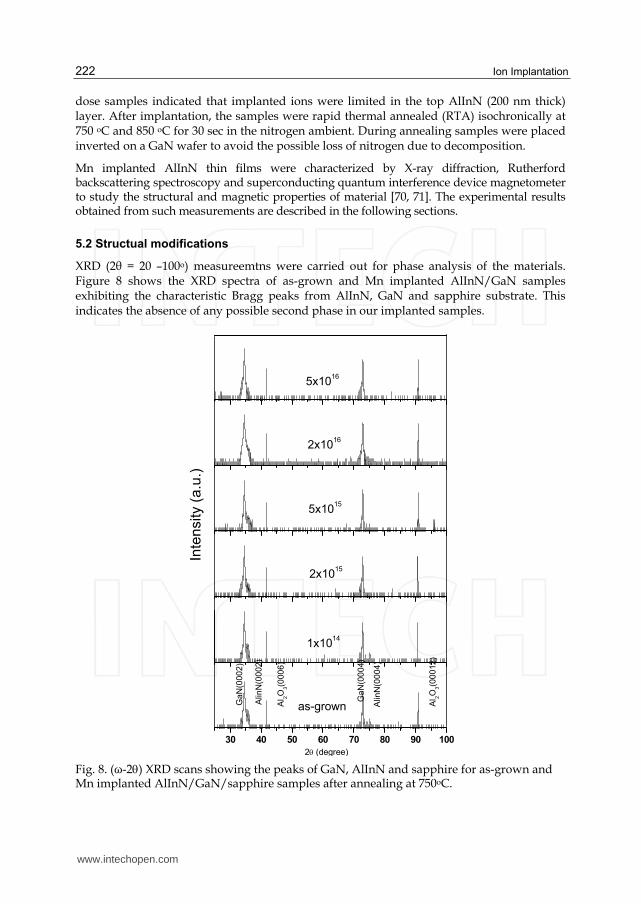
5.2 Structual modifications
XRD (2θ = 20 –100o) measureemtns were carried out for phase analysis of the materials. Figure 8 shows the XRD spectra of as-grown and Mn implanted AlInN/GaN samples exhibiting the characteristic Bragg peaks from AlInN, GaN and sapphire substrate. This indicates the absence of any possible second phase in our implanted samples.
30 40 50 60 70 80 90 100
Al 2
O3(0
00
12
)
GaN
(00
04)
2 (degree)
as-grownGa
N(0
00
2)
In
ten
sity (
a.u
.)
1x10¹⁴
2x10¹⁵
5x10¹⁵
2x10¹⁶
Al 2
O3(0
00
6)
Alin
N(0
004
)
Alin
N(0
002
)
5x10¹⁶
Fig. 8. (ω-2) XRD scans showing the peaks of GaN, AlInN and sapphire for as-grown and Mn implanted AlInN/GaN/sapphire samples after annealing at 750oC.
www.intechopen.com

Neon and Manganese Ion Implantation into AlInN
223
Figure 9 shows the (0002) symmetrical XRD spectra of as-grown and Mn implanted AlInN/GaN samples after annealing at 750 oC for 30 sec. GaN peak for all the samples appeared at 2θ=34.56o. AlInN peak was found at 2θ = 35.59o for as-grown samples but it appeared at different positions for the implanted samples. This AlInN peak shifted towards the lower angle side with increase in dose up to 5x1015 cm-2 and then it shifted back towards higher angle for higher doses. All the AlInN peaks, given in XRD spectra, were Lorentz fitted to extract the peak position.
34.0 34.5 35.0 35.5 36.0
as-grown
1014
2x10¹⁵
5x10¹⁵
9x10¹⁵
2x10¹⁶
5x10¹⁶
AlInN(0002)
2 (degree)
Inte
nsity (
a.u
.)
GaN(0002)
Fig. 9. X-Ray diffraction spectra from (0002) symmetric (ω-2) scans showing GaN and AlInN peaks of as-grown and Mn implanted AlInN/GaN samples after annealing at 750oC. AlInN peaks are shown Lorentz fitted.
Figure 10 shows the XRD spectra of as-grown and Mn implanted AlInN/GaN samples after subsequent annealing at 850 oC for 30 sec. A trend of shift in the position of AlInN peak, similar to the previous annealing, was observed for all the implanted samples. However, the increase in X-ray intensity of the peaks related to the GaN and AlInN was noted, which indicates the improved lattice recovery. No sizeable additional peak was seen on the lower angle side of GaN peak that indicates that either no or very small number of implanted ions have reached the buried GaN layer.
The perpendicular strain of implanted AlInN lattice relative to that of as-grown samples was calculated from the data extracted from the symmetric (0002) XRD scans by using the angular separation of substrate (GaN) and epilayer (AlInN) peaks. Figure 11 shows the perpendicular strain of AlInN layer for both the annealing steps. After first annealing at 750oC the strain increases with dose until it reaches to the maximum value for the sample implanted with dose of 2x1015 cm-2. It remains constant for further increase in dose up to 5x1015 cm-2 and then starts decreasing with the increase in dose. The strain follows the same trend after second annealing at 850 oC with a minor difference; instead of being constant it starts decreasing immediately after reaching to a saturation value. Another difference observed is the higher strain for samples implanted with doses 2x1016 cm-2 and 5x1016 cm-2 after annealing at 850 oC as compared to that noted after annealing at 750 oC.
www.intechopen.com

Ion Implantation
224
34.0 34.5 35.0 35.5 36.0 36.5
as-grown
1014
2x10¹⁵
5x10¹⁵
9x10¹⁵
2x10¹⁶
5x10¹⁶
AlInN(0002)
degree)
GaN(0002)
Inte
nsity (
a.u
.)
Fig. 10. X-Ray diffraction spectra from (0002) symmetric (ω-2) scans showing GaN and AlInN peaks for as-grown and Mn implanted AlInN/GaN samples after annealing at 850oC. AlInN peaks are shown Lorentz fitted.
0 100 200 300 400 500-0.4
-0.2
0.0
0.2
0.4
0.6
Pe
rpe
nd
icu
lar
str
ain
Dose (x1014
cm-2)
750oC
850oC
Fig. 11. Perpendicular strain extracted from XRD for as-grown and Mn implanted AlInN/GaN samples after both annealing steps of 750oC and 850oC. Solid lines are guides to eye.
5.3 Thermal annealing degradation of AlInN
RBS measurements were carried out to find the depth profile of elements of the samples. Figure 12 shows the random RBS spectra of as-grown and Mn implanted AlInN/GaN samples measured after annealing at 750 oC. The energy of alpha particles backscattered from the interface is indicated by an arrow labeled by Ga. The arrows labeled Al and In
www.intechopen.com

Neon and Manganese Ion Implantation into AlInN
225
indicate the energy of alpha particles backscattered from the respective atoms of aluminum and indium. The Mn signal was detected only in the spectrum of the samples implanted with the highest dose.
100 200 300 400
0
2000
4000
Mn
as-grown
1014
2x10¹⁵
5x10¹⁵
9x10¹⁵
2x10¹⁶
5x10¹⁶
Yie
ld (
a.u
)
Channel
Al
In
Ga
Fig. 12. RBS spectra of as-grown and Mn implanted AlInN after annealing at 750oC. Dose for all the samples is shown in cm-2.
RBS measurements were again performed on the same samples after next annealing at 850 oC for 30 sec to study the thermally activated atomic migration of the constituents of the samples. The RBS random spectra of as-grown and such post implanted annealed samples are given in figure 13.
100 200 300 400
0
500
1000
Ga
Yie
ld (
a.u
.)
Channel
as-grown
1014
2x10¹⁵
5x10¹⁵
9x10¹⁵
2x10¹⁶
5x10¹⁶
Al
In
Fig. 13. RBS random spectra for as-grown and Mn implanted AlInN samples after annealing at 850oC. Dose for all the samples is given in cm-2.
www.intechopen.com

Ion Implantation
226
The comparison of indium and aluminum peaks after both anneals presents an interesting behavior that highlights the effect of annealing on atomic migration in implanted samples. Figure 14 shows the blown up RBS spectra of indium peak for as-grown and implanted samples after both anneals. The vertical arrows show the energy position of alpha particles backscattered from indium atoms located in the region near to the surface.
Indium peak after annealing at 750 oC is found shifted to the lower energy side when compared to that of as-grown samples as shown in figure 14 (a). The RBS spectra of indium peak after 850 oC annealing is shown in figure 14 (b). The spectra are found quite different from those measured after first annealing. In this case the indium peak is found shifted to the high energy side with reduction of yield as compared to that of the as-grown samples. This observation indicates the out-diffusion of indium atoms towards the surface after this annealing. The behavior of the peak with increasing dose is similar to that of observed after first annealing but reduction in yield is high in this case.
360 380 400
0
200
400
600
380 400 420
400
600
800
1000
Channel
as-grown
1014
2x10¹⁵
5x10¹⁵
9x10¹⁵
2x10¹⁶
5x10¹⁶
as-grown
1014
2x10¹⁵
5x10¹⁵
9x10¹⁵
2x10¹⁶
5x10¹⁶
Yie
ld (
a.u
)
Channel
(a) (b)
Fig. 14. RBS spectra of as-grown and Mn implanted AlInN samples showing In peak after annealing at (a) 750oC (b) 850oC.
The comparative behavior of Al signal after both anneals is shown in the figure 15. After the first annealing, Al peak is observed truncated from the higher energy side for the samples irradiated with lower doses as compared to that of as-grown samples. The decrease in yield with increase in dose is observed, which is prominent for samples implanted with highest dose. The comparison of scans of as-grown and implanted samples given in figure 15 (b) shows a clear shift in the aluminum signal towards higher energy side for implanted samples. A drastic decrease in the yield of Al peak can also be noted after second annealing as compared to that of first annealing.
Figure 16 shows the blown up RBS spectra of interface region measured after both anneals. The presence of Ga peak in between the interface and indium peak is clearly noticed in the
www.intechopen.com

Neon and Manganese Ion Implantation into AlInN
227
RBS spectra of as-grown samples, which is found suppressed for the implanted samples with the increase in dose. The position of the interface edge for the implanted samples remained the same after first annealing but it was found shifted toward higher energy side after second annealing.
200 250
2000
2500
3000
3500
200 250 300
200
400
600
800
1000
1200
Channel
as-grown
1014
2x10¹⁵
5x10¹⁵
9x10¹⁵
2x10¹⁶
5x10¹⁶
as-grown
1014
2x10¹⁵
5x10¹⁵
9x10¹⁵
2x10¹⁶
5x10¹⁶
Yie
ld (
a.u
)
Channel
(a) (b)
Fig. 15. RBS spectra of as-grown and Mn implanted AlInN samples showing Al peak after annealing at (a) 750oC (b) 850oC.
320 340 360
0
1000
2000
300 320 340 360
0
200
400
600
800
Ga
Channel
as-grown
1014
2x10¹⁵
5x10¹⁵
9x10¹⁵
2x10¹⁶
5x10¹⁶
as-grown
1014
2x10¹⁵
5x10¹⁵
9x10¹⁵
2x10¹⁶
5x10¹⁶
Yie
ld (
a.u
)
Channel
Ga
(a) (b)
Fig. 16. RBS spectra of as-grown and Mn implanted AlInN samples showing Ga migration at the interface for annealing at (a) 750oC (b) 850oC
www.intechopen.com

Ion Implantation
228
Figure 17 shows the comparison of RBS spectra in the region of Mn signal that appears clearly in between channel numbers 300 and 330 in RBS spectra of AlInN sample implanted with highest dose of 5x1016 cm-2 after annealing at 750oC but it could not be detected after annealing 850oC.
280 290 300 310 320 330
1400
1600
1800
Yie
ld (
a.u
.)
Channel
as-grown
750oC anneal
850oC anneal
Mn signal
Fig. 17. RBS spectra showing the Mn signal in Mn implanted AlInN samples having dose 5x1016cm-2 after both anneals. Spectrum of as-grown sample is also given for comparison.
5.4 AlInN based diluted magnetic semiconductor
Magnetic properties of Mn implanted AlInN samples were studied using SQUID magnetometer by recording magnetization as a function of temperature and applied field. Hysteresis loops were recorded at 100 K and 300 K for implanted samples. Magnetic measurements were carried out on the samples implanted with doses 1x10¹⁴, 2x10¹⁵ and 2x1016cm-2 and subsequently annealed at 750o for 30 sec. The temperature dependence of magnetization (MT curves) of as-grown and implanted samples having different Mn concentrations (0.01, 0.2 and 2 at. %) is shown in figure 18. As-grown samples exhibited very weak signal with a paramagnetic behavior, presumably due to the impurities in the substrate. There is a clear difference of FC and ZFC magnetization observed up to 235 K for the samples having Mn concentration of 0.01 at. %. The samples having Mn concentration of 0.2 at.% show a strong magnetization with a difference in FC and ZFC magnetizations that extend up to 285 K. Similar trend was observed in the MT curves of the sample having the highest Mn concentration of 2 at.%. An apparent transition observed in MT curves of this sample at around 260 K which points to the presence of at least two magnetic phases with one having Curie point Tc at 260 K and the other above room temperature. The highest magnetization has been observed for this sample with difference in FC and ZFC magnetization curves that persists up to nearly room temperature.
www.intechopen.com

Neon and Manganese Ion Implantation into AlInN
229
0 50 100 150 200 250 300
0.1
0.2
1.2
1.3
1.4
3.6
3.8
4.0
4.2
4.4
1
2
3
4
FC
ZFCAs-grown
(a)
(b)
FC
ZFC1X10
14cm
-2
(c)2X10
15cm
-2
FC
ZFC
(d)
Temperature (K)
2X10¹⁶
cm-2
M (x10
-5em
u)
FC
ZFC
Fig. 18. FC and ZFC magnetization curves at applied field of 500 Oe for (a) as-grown and Mn implanted AlInN samples having Mn concentration of (b) 0.01 at. %, (c) 0.2 at. % and (d) 2 at. %.
Figure 19 shows the room temperature magnetization measurements as a function of applied field (MH loops). Clear hysteresis behavior is observed for all the samples. The values of saturation magnetization (Ms) have were to be 5.83, 25.4 and 27.92 emu/cm3 for AlInN samples having Mn atomic concentrations of 0.01%, 0.2% and 2% respectively. The values of effective magnetic moment per Mn atom (peff) were calculated to be 113, 24.6 and 2.67 ┤B/ion respectively. This shows a trend of increase in Ms and decrease in peff in AlInN samples with increase in Mn concentration. The difference in FC and ZFC magnetization values is an established tool to exclude the possibility of paramagnetic and diamagnetic contribution in the observed magnetic properties. For all the samples, the difference between FC and ZFC along with well defined hysteresis loop at 300 K is consistent with presence of ferromagnetic ordering at room temperature.
In order to explore the effects of Mn implantation on the structural properties of the material, we conducted detailed XRD and RBS studies. Using the shift in position of AlInN related XRD peak, we studied the strain in AlInN epilayer as a function of implantation dose and annealing temperature. After annealing at 750 oC, the strain increases with dose until it reaches a short plateau and then decreases with further increase in dose. Similar dose dependent behavior of the strain variation has been reported by Partyka et al for the argon implanted AlGaAs/GaAs [51].
The variation of strain with dose in our samples can be divided into three regimes (1) strain accumulation (2) strain saturation and (3) strain dispersion. In the first regime, during lowest implantation dose of 1014cm-2, point defects (vacancy, interstitial, substitutional, and antisite) dominate due to the atomic displacements. These defects are spread within the
www.intechopen.com

Ion Implantation
230
lattice, mostly away from one another. The interstitial-vacancy pairs accumulate around the route of the penetrating ion due to displacement of Al and In atoms from their regular sites. Most of the Mn ions are expected to rest on some of the interstitial sites during this implantation dose. Projectile Mn ions encounter In atoms rarely in their way due to low indium concentration in the samples but Ini (interstitial indium atoms) are still expected to be produced due to collective motion of the cascade atoms. With increase in the dose the defect density increases, which enhances the probability of interaction of new defects with old ones. This favors the clustering of individual defects causing the increase in the level of lattice deformation. All such events will increase the perpendicular strain and cause the lattice to expand accordingly. This situation will persist until the dose of 2x1015 cm-2 at which the strain saturates. Interaction probability of newly produced defects with existing defects is maximized at a particular defect density in this situation. This saturation state is maintained in dose range 2x10¹⁵ to 5 x1015 cm-2. The implantation dose of 2x1015 cm-2 seems to be critical for providing a driving force, which causes the annihilation of (vacancy, interstitial) defects and prevent the increase in strain. Mn ions have more probability to occupy substitutional sites in this atmosphere. The competition between defect creation and annihilation limits the net increase in the strain in this region. With further increase in dose, third regime starts where a decrease in strain is observed. This decrease of strain is attributed to the migration of defects into sinks (cavities, dislocation loops, grain boundaries etc). Defect clusters after attaining a critical size may have collapsed to minimize the thermodynamic free energy of the system. This collapse may produce either the increase of substitutional efficiency or capturing of defects by cavities or conversion of defects into local amorphous zones in the lattice. The strain relaxation will be the consequence of all such events. Most of Mn ions are expected to occupy the substitutional sites into the cationic sublattice of Al and In atoms in this regime of dose.
-1000 -500 0 500 1000-30
-20
-10
0
10
20
30
M(e
mu
/cm
3)
H(Oe)
0.01 at. %
0.2 at. %
2 at. %
T= 300K
Fig. 19. Room temperature magnetization as a function of applied magnetic field for AlInN samples having different Mn concentrations.
www.intechopen.com
Neon and Manganese Ion Implantation into AlInN
231
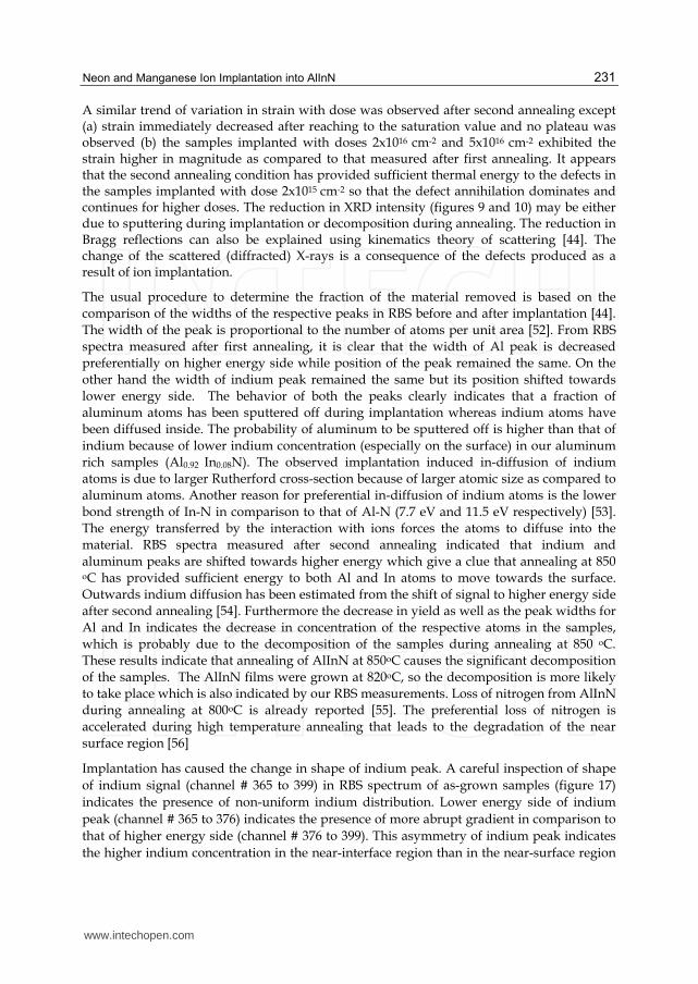
A similar trend of variation in strain with dose was observed after second annealing except (a) strain immediately decreased after reaching to the saturation value and no plateau was observed (b) the samples implanted with doses 2x1016 cm-2 and 5x1016 cm-2 exhibited the strain higher in magnitude as compared to that measured after first annealing. It appears that the second annealing condition has provided sufficient thermal energy to the defects in the samples implanted with dose 2x1015 cm-2 so that the defect annihilation dominates and continues for higher doses. The reduction in XRD intensity (figures 9 and 10) may be either due to sputtering during implantation or decomposition during annealing. The reduction in Bragg reflections can also be explained using kinematics theory of scattering [44]. The change of the scattered (diffracted) X-rays is a consequence of the defects produced as a result of ion implantation.
The usual procedure to determine the fraction of the material removed is based on the comparison of the widths of the respective peaks in RBS before and after implantation [44]. The width of the peak is proportional to the number of atoms per unit area [52]. From RBS spectra measured after first annealing, it is clear that the width of Al peak is decreased preferentially on higher energy side while position of the peak remained the same. On the other hand the width of indium peak remained the same but its position shifted towards lower energy side. The behavior of both the peaks clearly indicates that a fraction of aluminum atoms has been sputtered off during implantation whereas indium atoms have been diffused inside. The probability of aluminum to be sputtered off is higher than that of indium because of lower indium concentration (especially on the surface) in our aluminum rich samples (Al0.92 In0.08N). The observed implantation induced in-diffusion of indium atoms is due to larger Rutherford cross-section because of larger atomic size as compared to aluminum atoms. Another reason for preferential in-diffusion of indium atoms is the lower bond strength of In-N in comparison to that of Al-N (7.7 eV and 11.5 eV respectively) [53]. The energy transferred by the interaction with ions forces the atoms to diffuse into the material. RBS spectra measured after second annealing indicated that indium and aluminum peaks are shifted towards higher energy which give a clue that annealing at 850 oC has provided sufficient energy to both Al and In atoms to move towards the surface. Outwards indium diffusion has been estimated from the shift of signal to higher energy side after second annealing [54]. Furthermore the decrease in yield as well as the peak widths for Al and In indicates the decrease in concentration of the respective atoms in the samples, which is probably due to the decomposition of the samples during annealing at 850 oC. These results indicate that annealing of AlInN at 850oC causes the significant decomposition of the samples. The AlInN films were grown at 820oC, so the decomposition is more likely to take place which is also indicated by our RBS measurements. Loss of nitrogen from AlInN during annealing at 800oC is already reported [55]. The preferential loss of nitrogen is accelerated during high temperature annealing that leads to the degradation of the near surface region [56]
Implantation has caused the change in shape of indium peak. A careful inspection of shape of indium signal (channel # 365 to 399) in RBS spectrum of as-grown samples (figure 17) indicates the presence of non-uniform indium distribution. Lower energy side of indium peak (channel # 365 to 376) indicates the presence of more abrupt gradient in comparison to that of higher energy side (channel # 376 to 399). This asymmetry of indium peak indicates the higher indium concentration in the near-interface region than in the near-surface region
www.intechopen.com

Ion Implantation
232
of as-grown samples. It is clear that implantation has modified the profile of indium peak. The RBS spectrum of indium peak of implanted samples depicts that (a) shape has become symmetrical and (b) peak position is shifted to lower energy side. These observations indicate the redistribution of indium atoms due to knock-in effects caused by impact of implanted Mn ions with indium atoms. The analysis of peak shape points to the presence of nearly equal gradient on lower energy side (channel # 356 to372) and on higher energy side (channel # 372 to 389). On the other hand, shift of peak towards lower energy side indicates the indium atoms have migrated toward interface. Both these observations points to a noticeable effect, that the implantation has caused the change in depth profile of indium in such a way that more indium is concentrated near the interface than in the near-surface region.
The presence of Mn signal (figure 17) after first annealing and suppression after second annealing can be explained by taking into account the atomic diffusion caused by high temperature annealing. Like Al and In atoms, Mn has also out-diffused and most probably have evaporated during high temperature annealing. Such evaporation of implanted atoms from GaN during annealing has been reported by Lorenz et al [57].
The presence of Ga peak in between the interface and indium peak can be explained by considering the bad quality of the interface resulting from the diffusion of Ga atoms into the AlInN layer during high temperature growth at 820 oC. The presence of Ga in the top layer near the interface may lead to the formation of a fuzzy interlayer of AlInGaN to shape the sample in the form of AlInN/AlInGaN/GaN structure. The suppression of Ga peak observed after first annealing is due to the in-diffusion of Ga atoms towards the GaN buffer during the energetic ion implantation. This may have reduced the interlayer thickness thereby improving quality of the interface. During second annealing out-diffusion of Ga atoms is expected similar to that Al and In that lead to increase in thickness of the fuzzy interlayer. The interface signal is now coming from the place up to which Ga atoms have diffused upwards. Therefore the observed shift of the interface towards higher energy side is the consequence of the upwards Ga diffusion. The different behavior of interface after both anneals is understandable by considering the annealing temperature below and above the growth temperature. It should be interesting to compare results of our magnetic measurements with that of Mn doped AlN. Saturation magnetization reported for single phase AlMnN with Mn concentration of 1 at. % is ~0.2 emu/cm3 [58], which is much smaller as compared to the value observed for our samples even having lowest Mn concentration of 0.01at. %. The reason for this drastic difference in magnetic behavior can be explained by taking into account the lattice parameters which have significant effect on the magnetic properties. The lattice constants of our as-grown AlInN samples are c = 5.135 Å, a = 3.118 Å, which are larger as compared to that of AlN (c = 4.982 Å, a = 3.112 Å). Fermi level (EF) of the AlInN having lattice constants larger than that of AlN will be lower in energy [59]. With the shift of EF towards valence band, the strength of bonds reduces due to formation of vacancies. The reduction in bond strength is another explanation of ferromagnetism enhancement in Mn-AlInN system as compared to Mn-AlN. Decrease in bond strength due to indium incorporation into AlN will produce more vacancies, which makes AlInN comparatively a favorable environment for Mn to occupy the substitutional sites rather than making clusters. The tendency of self-compensation by Mn at interstitial sites is believed to be weak when substitutional Mn acceptor level shifts deeper into the band gap of the wide band gap materials [60] that also support the probability of Mn to occupy the substitutional sites. Our XRD measurements (figure 8) provide evidence that no second phase (like;
www.intechopen.com

Neon and Manganese Ion Implantation into AlInN
233
Ferromagnetic MnxN, Antiferromagnetic MnxNy and ferromagnetic AlMn) are responsible for the observed magnetism in our implanted samples. It is reported that the formation of clusters takes place beyond 2% of Mn concentration [61] but Mn concentration in our samples is below this limit, therefore we expect the role of secondary phases, if any, is insignificant and ferromagnetic ordering in our samples is dominated by substitutional incorporation of Mn in the AlInN lattice.
The value of effective magnetic moment per Mn ion for our implanted samples is found extraordinarily large as compared to the Mn atomic moment of 5µB/ion, for two samples having lowest Mn concentration. The colossal magnetic moment in Gd implanted GaN has already been observed by Dhar et al [62] who have found extraordinary large values of effective magnetic moment per Gd atom (peff). The trend of dose dependence of Ms as observed in our samples, is similar to that of observed by Dhar et al for Gd implanted GaN. They developed a phenomenological model [63] to get a quantitative understanding of the range of spin polarization of GaN matrix by randomly positioned Gd atoms by assuming a rigid sphere of influence around every magnetic atom. The value of saturation magnetization for the Mn implanted samples based on their model is given by the following equation.
12
Mn
n n
N
S M M o o o nn
M p N p vN p N nv
Where No is the concentration of AlInN matrix atoms, v is the volume of each sphere, v is the volume fraction occupied by each sphere, i.e. 1 exp( )
nMv vN and
( )
!n n
nM vM
n
nNv e
n is the volume fraction of the regions contained within ‘n’ spheres. For
the lower Mn concentrations, most of the spheres are assumed well separated and peff has its maximum value. Since v is an increasing function of NMn, the value of Ms increases with increase in concentration of implanted ions and crosses the percolation threshold when v approaches to unity for a certain concentration of ions. Finally, at very high Mn concentrations the entire matrix becomes polarized and first term in the equation starts to dominate over the rest of the terms and peff further decreases. Carrier mediated ferromagnetism does not appear to be applicable in the III-nitrides having transition metal related energy level very deep into the band gap [64]. Our implanted samples are expected to have low carrier concentration and resistive in nature like other transition metals implanted nitrides [65, 66]. This suggests that charge carriers are localized by the defects with random distribution of their localization centers in the lattice. It has been reported that ion implantation into nitrides and AlInN produces highly resistive regions and causes the decrease in carrier concentration [67]. We therefore suggest that ferromagnetic exchange interaction in our implanted samples is mediated by localized electrons that form bound magnetic polarons (BMP) whose overlap produces a spin-split Mn impurity band [12]. Radius of BMP increases logarithmically with decreasing temperature so that long range ferromagnetic ordering appears at low enough temperatures due to the overlapping of BMPs. Diluted magnetic semiconductors having random distribution of magnetic impurities are favorable to produce overlapping of BMPs. We calculated the radius of hydrogenic orbital of electron in BMP system for Al0.92In0.08N using aB= ε*(me/m*) x 0.53 Å [ ref. 12] and found its value to be 9.23 Å. Hydrogenic radius of electron in BMP system for AlN is
www.intechopen.com

Ion Implantation
234
reported to be 8.5 Å [68]. Large value of BMP radius increases the probability of BMP overlapping to mediate the ferromagnetic coupling, which is another indicator of enhanced ferromagnetism in implanted AlInN as compared to the AlN. The values calculated for inter Mn distance by assuming the uniform Mn distribution in the whole DMS layer are 19.6 nm, 2.58 nm and 1.18 nm for samples having Mn concentrations of about 0.01%, 0.2% and 2% respectively. Although these values are larger than the radius of BMP (0.92nm) but the values of inter Mn distances would be smaller, especially in the central region of DMS layer, if the true Gaussian distribution of implanted Mn is taken into account. Therefore, we are justified to assume that BMP is a possible mechanism for ferromagnetic ordering in Mn implanted AlInN samples.
6. Summary
The effects of neon and manganese ion implantation into MOCVD grown wurtzite AlInN have been studied in detail. Ne ions with doses 1x10¹⁴, 2x10¹⁵, 5x10¹⁵, 9x10¹⁵ /cm2and Mn with doses 1x10¹⁴, 2x10¹⁵, 5x10¹⁵, 9x10¹⁵, 2x10¹⁶ and 5x10¹⁶ ions/cm2 were implanted into the materials. After implantation, AlInN samples at 750oC and 850 oC using rapid thermal annealing processor. The structural, optical and magnetic characterization were performed with Rutherford backscattering spectroscopy (RBS), X-Ray diffraction (XRD), vibrating sample magnetometer (VSM) and superconducting quantum interference device (SQUID).
The XRD spectra of Ne and Mn implanted AlInN exhibits a systematic shift toward the lower angle side and a decrease in intensity of peak related to AlInN with respect to that of GaN with increase in dose up to 5x1015 cm-2. The shift of the peak was found reversed for higher doses. Strain obtained from the shift of AlInN peak was found increased with dose until it reached a saturation value and after that it started decreasing with further increase in dose. RBS measurements indicated the atomic diffusion of In, Al, Ga and Mn in manganese implanted AlInN. The in- and out-diffusion of atoms has been observed after annealing at 750oC and 850oC respectively. A strong decomposition of AlInN samples has been noticed after annealing at 850oC. This points to the unsuitability of annealing of Mn implanted AlInN samples at temperature higher than the growth temperature of samples. Magnetic characterization carried out by SQUID magnetometer revealed the presence of well defined magnetic hysteresis at 300 K and a difference in FC and ZFC curves up to room temperature. These observations indicated the presence of room temperature ferromagnetic properties in Mn implanted AlInN samples which are prerequisites for DMS materials.
7. References
[1] Starosta K. Phys. Status Solidi a 68, K55 (1981). [2] Kubota, Y. Kobayashi and K. Fujimoto, J. Appl. Phys. 66, 2984 (1989) [3] C. Hums, J. Blasing, A. Dadgar, A. Diez, T. Hempel, J. Christen, A. Krost, K. Lorenz and
E. Alves, Appl. Phys. Lett. 90, 022105 (2007) [4] Tae Su Oh, Jong Ock Kim, Hyun Jeong, Yong Seok Lee, S Nagarajan, Kee Young Lim,
Chang-Hee Hong and Eun-Kyung Suh, J. Phys. D: Appl. Phys. 41, 095402 (2008) [5] Hadis Morkoc, Nitride semiconductors and devices, Springer (1999) [6] O.Manasreh, III-nitride semiconductors: electrical, structural and defects properties, (2000). [7] O. Ambacher. J. Phys. D: Appl. Phys. 31, 2563 (1998) [8] J.-F. Carlin and M. Ilegems, Appl. Phys. Lett. 83, 668(2003) [9] R. Butte et al, J. Phys. D: Appl. Phys. 40, 6328 (2008)
www.intechopen.com

Neon and Manganese Ion Implantation into AlInN
235
[10] S.J. Pearton et al, Physica B 340–342, 39 (2003) [11] Pearton S J, Vartuli C B, Zolper J C, Yuan C and Stall R A, Appl. Phys. Lett. 67, 1435 (1995) [12] J. M. D. Coey, M. Venkatesan and C. B. Fitzgerald, Nature mater. 4, 173 (2005) [13] G Schmidt and L WMolenkamp, Semicond. Sci. Technol. 17, 310 (2002) [14] Igor Zutic, Jaroslav Fabian and S. Das Sarma, REV. MOD. PHY. 76, 33 (2004) [15] A. H. Macdonald, P. Schiffer and N. Samarth, nature materials. 4, 195 (2005). [16] J. K. Furdyna. J. Appl. Phys. 64, R29 (1998) [17] S. J. Pearton et al. J. Phys.:Condes. Matter. 16, R209 (2004) [18] Dietl T, Ohno H, Matsukura F, Cibert J and Ferrand D, Science 287, 1019 (2000) [19] S. Sonoda, S. Shimizu, T. Sasaki, Y. Yamamoto and H. Hori, J. Cryst. Growth. 237-239,
1358 (2002). [20] K. Wang, R. W. Martin, E. Nogales, P. R. Edwards, K. P. O’Donnell, K. Lorenz, E. Alves
and I. M. Watson, Appl. Phys. Lett. 89, 131912 (2006) [21] R. W. Martin et al, phys. stat. sol. (c) 6, 1927 (2006) [22] B. M. Paine, N.N. Hurvitz, and V. S. Speriosu, J. Appl. Phys. 61, 1335 (1987) [23] K. Lorenz, N. Franco E. Alves, I. M. Watson, R.W. Martin, and K. P. O’Donnel, Phys.
Rev. Lett. 97, 085501 (2006) [24] S. J. Pearton, C. R. Abernathy, P. W. Wisk, W. S. Hobson, and F. Ren, Appl. Phys. Lett.
63, 1143 (1993) [25] A. Buyanova, Mt. Wagner, W. M. Chen, B. Monemar, J. L. Lindstrom, H. Amano and I.
Akasaki, Appl. Phys. Lett. 73, 2968 (1998) [26] H. X. Jiang, S. X. Jin, J. Li, J. Shakya, and J. Y. Lin, Appl. Phys. Lett. 78, 1303 (2001) [27] F. Briegleb and A. Geuther Ann. Chem. 123, 228 (1862) [28] Tae Su Oh, Jong Ock Kim, Hyun Jeong, Yong Seok Lee, S Nagarajan, Kee Young Lim,
Chang-Hee Hong and Eun-Kyung Suh, J. Phys. D: Appl. Phys. 41, 095402 (2008). [29]V. Yu. Davydov, A. A. Klochikhin, V. V. Emtsev, D. A. Kurdyukov, S. V. Ivanov, V. A.
Vekshin, F. Bechstedt, J. Furthmüller, J. Aderhold, J. Graul, A. V. Mudryi, H. Harma, A. Hashimoto, A. Yamamoto, and E. E. Haller, Phys. Status Solidi B 234, 787 (2002).
[30] Q. Guo and A. Yoshida, Jpn. J. Appl. Phys. 33, 2453 (1994) [31] Nicolay S, Carlin J-F, Feltin E, Butt´e R, Mosca M, Tchernycheva M, Nevou L, Julien F
H, Grandjean N and Ilegems M Appl. Phys. Lett. 87, 111106 (2005) [32] Christmann G, Simeonov D, Butt´e R, Feltin E, Carlin J-F and Grandjean N Appl. Phys.
Lett. 89, 261101 (2006) [33] L. Vegard, Z. Phys. 5, 17 (1921) [34] T. Seppanen, L. Hultman, J. Birch, M. Beckers and U. Kreissig, J. Appl. Phys. 101, 43519
(2007). [35] M. J. Lukitsch, Y. V. Danylyuk, V. M. Naik, C. Huang, G. W. Auner, L. Rimai and R.
Naik Appl. Phys. Lett. 79, 632 (2001) [36] V S Harutyunyan, A P Aivazyan, E R Weber, Y Kim, Y Park and S G Subramanya, J.
Phys. D: Appl. Phys. 34, A35–A39 (2001). [37] D. Keith Bowen and Brian K. Tanner, X-Ray metrology in semiconductor
manufacturing, Taylor & Francis group, (2006) [38] L. T. Romano, C. G. Van de Walle, J. W. Ager III, W. Gotz and R. S. Kern, J. Appl. Phys.
87, 7745 (2000). [39] S.O. Kucheyev, J.S. Williams, S.J. Pearton, Materials Science and Engineering Reports
33, 51(2001) [40] Lindhard, Scharff and Schiottm Mat. Phys. Medd. Dan. Vid. Selsk. 33 (1963). [41] www.SRIM.org
www.intechopen.com

Ion Implantation
236
[42] E. Alves, U. Wahl, M.R. Correia, S. Pereira, B. De Vries, A. Vantomme, Nuclear Instruments and Methods in Physics Research B 206, 1042 (2003).
[43] W Liu, J F Wang, J J Zhu, D S Jiang and H Yang, J. Phys. D: Appl. Phys. 40, 5252 (2007). [44] A. Seidel, S. Massing, B. Strehlau, and G. Linker, Phys. Rev. B, 38, 2273 (1988) [45] A. Luukkainen, J. Keinonen and M. Erola, Phys. Rev. B. 32, 4814 (1985) [46] C. A. Cima, H. Boudinov, J. P. de Souza, Yu. Suprun-Belevich and P. F. P. Fichtner, J.
Appl. Phys. 88, 1771(2000) [47] J. H. Evans, Nucl. Instrum. Methods Phys. Res. B. 196, 125 (2002). [48] M. Chicoin, S. Roorda, R. A. Masut and P. Desjardins, J. Appl. Phys. 94, 6116 (2003) [49] M. Luysberg et al., J. Appl. Phys. 92, 4290 (2002) [50] V. A. Joshkin, C. A. Parker, S. M. Bedair, L. Y. Krasnobaev, J. J. Cuomo, R. F. Davis, A.
Suvkhanov, Appl. Phys. Lett. 72, 2838 (1998) [51] P. Partyka, R. S. Averback, D. V. Forbes, J. J. Coleman and P. Ehrhart, J. Appl. Phys. 83,
1265 (1998) [52] W. K. Chu, J. W. Mayer, and M. A. Nicolet, Backscattering Spectroscopy (Academic,
New York, 1978) [53] A. Kerr. CRC Handbook of Chemistry and Physics (CRC Press, Boca Raton, FL, 1990) [54] Y.Q. Wang, M. Curry, E. Tavenner, N. Dobson and R.E. Giedd, Nuclear Instruments
and Methods in Physics Research B. 219–220, 798 (2004). [55] J. Karpinski, J. Jun, and S. Porowski, J. Cryst. Growth. 66, 1(1984). [56] S. O. Kucheyev, J. S. Williams, C. Jagadish, G. Li and S. J. Pearton, Appl. Phys. Lett.76,
3899 (2000). [57] K. Lorenz, U. Wahl, E.Alves, T. Wojtowicz, P. Ruterana, S. Ruffenach, O. Briot,
Superlattice and microstructures. 36, 737 (2004) [58] R. M. Frazier, G. T. Thaler, B.P. Gila, J. Stapleton, M.E. Overberg, C.R. Abernathy, S.J.
Pearton, F. Ren, And J.M. Zavada, J. Elect. Mater. 34, 365 (2005) [59] Galanakis, P. H. Dederichs and N. Papanikolaou, Phys. Rev. B. 66, 134428 (2002). [60] J. Masek, J. Kudrnovsky, F. Maca, Jairo Sinova, A. H. MacDonald, R. P. Campion, B. L.
Gallagher, and T. Jungwirth, Phys. Rev. B. 75, 045202 (2007) [61] Y. L. Soo, G. Kioseoglou, S. Kim, S. Huang, Y. H. Kao, S. Kuwabara, S. Owa, T. Kondo
and H. Munekata: Appl. Phys. Lett. 79, 3926 (2001) [62] S. Dhar, T. Kammermeier, A. Ney, L. Perez, K. H. Ploog, A. Melnikov and A. D. Wieck,
Appl. Phys. Lett. 89, 062503 (2006) [63] S. Dhar, L. Perez, O. Brandt, A. Trampert, K. H. Ploog, J. Keller and B. Beschoten, Phys.
Rev. B. 72, 245203 (2005) [64] Tobias Graf, Sebastian T. B. Goennenwein, and Martin S. Brandt, phys. stat. sol. 239, 277
(2003) [65] A. Y. Polyakov, N. B. Smirnov, A. V. Govorkov, N. V. Pashkova, A. A. Shlensky, S. J.
Pearton, M. E. Overberg, C. R. Abernathy, J. M. Zavada, R. G. Wilson, J. Appl. Phys. 93, 5388 (2003)
[66] R. M. Frazier, G. T. Thaler, C. R. Abenathy, S. J. Pearton, M. L. Nakarmi, k. b. Nam, J. Y. Lin, H. X. Jiang, J. Kelly, R. Rairigh, A. F. Hebard, J. M. Zavada and R. G. Wilson, J. Appl. Phys. 94, 4956 (2003)
[67] S. J. Pearton, Mater. Sci. Rep. 4, 313 (1990) [68] Jun Zhang, S H Liou and D J Sellmyer, J. Phys.: Condens. Matter. 17, 3137 (2005). [69] Abdul Majid, Akbar Ali, J. J. Zhu and Y. T. Wang, J Mater Sci: Mater Electron. 20:230 (2009) [70] Abdul Majid, Akbar Ali, J J Zhu and Y T Wang, J. Phys. D: Appl. Phys. 41, 115404 (2008) [71] Abdul Majid Rehana Sharif J.J. Zhu Akbar Ali, Appl. Phys. A 96, 979 (2009) and Abdul
Majid, Rehana Sharif, Akbar Ali, and Jian Jun Zhu, Jpn. J. Appl. Phys. 48, 040202 (2009)
www.intechopen.com

Ion ImplantationEdited by Prof. Mark Goorsky
ISBN 978-953-51-0634-0Hard cover, 436 pagesPublisher InTechPublished online 30, May, 2012Published in print edition May, 2012
InTech EuropeUniversity Campus STeP Ri Slavka Krautzeka 83/A 51000 Rijeka, Croatia Phone: +385 (51) 770 447 Fax: +385 (51) 686 166www.intechopen.com
InTech ChinaUnit 405, Office Block, Hotel Equatorial Shanghai No.65, Yan An Road (West), Shanghai, 200040, China
Phone: +86-21-62489820 Fax: +86-21-62489821
Ion implantation presents a continuously evolving technology. While the benefits of ion implantation are wellrecognized for many commercial endeavors, there have been recent developments in this field. Improvementsin equipment, understanding of beam-solid interactions, applications to new materials, improvedcharacterization techniques, and more recent developments to use implantation for nanostructure formationpoint to new directions for ion implantation and are presented in this book.
How to referenceIn order to correctly reference this scholarly work, feel free to copy and paste the following:
Abdul Majid (2012). Neon and Manganese Ion Implantation into AlInN, Ion Implantation, Prof. Mark Goorsky(Ed.), ISBN: 978-953-51-0634-0, InTech, Available from: http://www.intechopen.com/books/ion-implantation/neon-and-manganese-ion-implantation-into-alinn