a-4 designing tr module systems with ads -...
TRANSCRIPT

Agilent EEsof EDAPage 1
Designing TR Module Systems with ADS
Anurag BhargavaApplication Engineer EEsof EDA
Agilent TechnologiesBangalore, India
Agilent EEsof EDA
Objective
• Main objective of this presentation is to….. – Show ADS capabilities as a complete Design Platform for high frequency
applications– Clearly differentiate ADS from some of the other point tools which often rely
on socket based approach resulting in disconnected flow involving various vendors and low efficiency
– Outline key value propositions of ADS over other products in markets to design System, Circuit and Electromagnetic level etc all under one environment
– Demonstrate a very practical approach to design unique systems such as TR (Transmit/Receive) Module which is used in most of the modern day A/D systems e.g. Active Phased Array Radar
Page 2

Agilent EEsof EDA
Presentation Scope
• This presentation will mainly focus on the Transmit mode analysis of TR Module due to time constraint but the idea presented here could be very easily extended to analyze Receive mode as well.
• Main idea is to show how ADS can be used as a single design platform to perform some of the very complicated jobs such as System Designs, File Sweeping operations, Antenna Array and Co-simulation of complete system consisting of System/Circuit along with Antenna Array, Beam Steering which is pretty unique to ADS
• There are other things mentioned in further work slides which can be surely done in order to take this design much more closer to real system design/validation job. Those point s could be easily accomplished within ADS without having the need for any 3rd party plugins/sockets etc but outside the scope of the current presentation. Some of the points mentioned such as Amplifier behavioral modeling (P2D/S2D/X-parameters) etc are again unique to ADS which is non-existing in competitive softwares.
Page 3
Agilent EEsof EDA
Agenda
• TR Module Overview & Key Components
• TR Module System Simulation
• TR Module with MMIC components
• Pulsed RF Simulation of TR Modules
• Patch Array Antenna
• TR Module with Patch Array Antenna
Page 4

Agilent EEsof EDA
T/R module sizing and frequency
T/R modules are sized to fit within the lattice of a phase array, which is a function of frequency.
A good rule of thumb is that within the plane of the array, the modules must stack together to meet a half-wavelength spacing. At 10 GHz this is 1.5 cm, or about 600 mils. Depending on the system design the module might be close to 1/2 wavelength in one dimension, and much less in the other; quite often the module must be mounted to a structural member or heat sink which takes up considerable percentage of the lattice.
Source: http://www.microwaves101.com/encyclopedia/transmitreceivemodules.cfm
Page 5
Agilent EEsof EDA
Typical TR Module Block Diagram
Page 6
Digital Phase Shifter
Digital Attenuator TR Switch 1
LNA Stage 1 & 2
Driver + PA
Limiter or Rx Protection Switch
Duplexer Coupler
Tx In
Tx Power Monitoring
Tx Out Rx In
Rx Out

Agilent EEsof EDA
Key Components of TR ModuleDigital Phase shifter
The phase shifter supplies the incremental phases to each element that is what drives the beam in different directions. Because phase shift is required in both transmit and receive, it is usually placed in a path that is common. In this case the phase shifter can be a passive reciprocal device (it usually is). It is possible to design an active phase shifter.
Phase shifters have phase errors, they are not perfect. But a not-so-well understood phenomenon of phase shifters is that their the phase errors can increase significantly when presented with a poor, frequency dependent, VSWR.
By taking the “real-world” loads that the phase shifter might be seeing into account early in the design phase, time-to-market and costs can be reduced significantly.
Page 7
Agilent EEsof EDA
Key Components of TR Module
Attenuator
The attenuator is used to add an amplitude taper across the array, to reduce side lobes. This is typically only done in receive mode, in transmit you want to splash as much radiation as you can. The attenuator often performs a second function of aligning the amplitudes of the individual elements.
Typically a digital attenuator is used in modern TR module systems.
Page 8

Agilent EEsof EDA
Key Components of TR Module
Duplexer
The duplexer is what allows the antenna to be shared between transmit and receive. It can be a ferrite circulator, or sometimes just a SPDT switch. In the case of a circulator, this is not a solid-state component, so it doesn't have to be within a hermetic housing. Sometimes we might see the T/R module's circulator outside the housing.
One other issue that the duplexer has to deal with is that at extreme scan angles, the VSWR of the antenna can get ugly. When this mismatch is passed on to the Power Amp, it's power can degrade due to load pull effects (worse than the straight mismatch loss). If the LNA presents a matched load during transmit, this is not a problem.
Page 9
Agilent EEsof EDA
Key Components of TR Module
Limiter / Receiver Protection Switch (RPS)
The Limiter prevents damage to the low noise amplifier during transmit or whenever stray radiation is present.
The Limiter/RPS often performs a second important function. It provides a termination to the duplexer/circulator during transmit, to absorb power that reflects from the antenna. Significant power can be reflected at large scan angles.
Page 10

Agilent EEsof EDA
Key Components of TR Module
Low Noise Amplifier (LNA)
The LNA sets the noise figure of the system, but all losses between the antenna and the LNA add to the overall noise figure and must be minimized.
In the picture shown above, two LNAs are used in series.
In order to maximize the sensitivity of the T/R module, every effort is made to locate the first LNA and the power amp as close as possible to the antenna to minimize attenuation of long transmission lines.
Sometimes an LNA is designed so that it provides a good impedance match when it is biased off.
Page 11
Agilent EEsof EDA
Key Components of TR Module
High-Power Amplifier (HPA)
The high-power amplifier is the biggest and most expensive part of a T/R module. It also is the primary source of waste heat that you have to dump overboard.
Often the power amp uses two chips and combines them with quadrature or in-phase Wilkinson couplers. The attraction of quadrature is that the impedance looking into the combined device is well matched.
Page 12

Agilent EEsof EDA
Key Components of TR Module
Modulation circuitry
T/R modules must be switched from transmit to receive quickly. The transmit gain path is turned off during receive cycle, and the receive amplifier path is biased off during transmit. This is almost always done by circuitry that turns off the drain current to the amplifiers that must be turned off. It is theoretically possible to modulate the amplifiers using the gate voltage, but this is almost never done, probably because any noise on the gate due to settling time of the modulation waveform will have a much bigger effect than ringing on the drain voltage.
P-channel MOSFETs are usually used to turn the amplifiers on and off. These offer a combination of low on-resistance (just a few milliohms!).
Page 13
Agilent EEsof EDA
Key Components of TR Module
Charge storage capacitance
Because the T/R element must be quickly switched, and the power supply is electrically far away, charge storage capacitors are used to maintain the amplifier bias voltages during the pulse.
An acceptable voltage droop for a power amplifier during pulsed operation is 5%, which will drop the power by a similar amount (5%, or about a quarter of a dB).
Question: What charge storage do you need for a 10 usec pulse to power a 10W power amp running at 8 volts and 5 amps peak?
Page 14
Answer: 125 uF

Agilent EEsof EDA
Key Components of TR Module
Beam steering digital circuitry
The phase shifters in the array must be set to specific values to control the beam position, this is no easy task and usually takes an distributed computer to get it done quickly and efficiently. This is often called the beam steering computer.
Housing
The housing that surrounds the T/R module is usually hermetic to assure a long and healthy life. The material is usually chosen to match the thermal expansion coefficient of the materials that are used within (i.e GaAs, silicon, various ceramics). This is one of the cost drivers of the technology.
The housing is usually the single biggest contributor to the mass of the overall T/R module. This is not a problem for ground based systems, but for airborne applications (or space!)
Page 15
Agilent EEsof EDA
Key Components of TR Module
Substrates
T/R modules typically use microstrip interconnects, by CPW and even stripline are possible. The substrates inside the module are usually ceramic, often a form of alumina is used.
Built-in test (BITE)
About an hour or two after the first phased array went to test, someone must have asked “There's a problem with the array, how do we know which module is bad?”
And so the T/R module usually has some form of built-in test circuit to verify its health. We can't test for everything, but the one thing that probably will fail the fastest is the power amplifier, which may be due to it's self-heating.
If you look at the T/R module block diagram on slide 17, you will notice a coupler circuit after Duplexer, this is for built-in test.
Page 16

Agilent EEsof EDA
Agenda
• TR Module Overview & Key Components
• TR Module System Simulation
• TR Module with MMIC components
• Pulsed RF Simulation of TR Modules
• Patch Array Antenna
• TR Module with Patch Array Antenna
Page 17
Agilent EEsof EDA
TR Module - System Level Analysis
Page 18
Digital Phase Shifter
Digital Attenuator
TR Switch
LNA Stage 1 and 2 Rx Protection Switch
Driver and Power Amp
Tx Power MonitoringDuplexer

Agilent EEsof EDA
TR Module – System Level Results
Page 19
Agilent EEsof EDA
TR Module – Ideal Digital Attenuator Sweep
Page 20
• Digital Attenuator model is swept from 0 – 31.5 dB in 0.5 dB steps (64 states)
• As expected system O/P power is decreasing linearly with attenuator value

Agilent EEsof EDA
TR Module – Ideal Phase Shifter Sweep
Page 21
• Digital Phase Shifter model is swept from 0 – 90 deg in 5.625 deg steps (16 states) just to characterize system performance
• In actual system we will use 6-bit Digital Phase Shifter which will make it possible to have phase shift from 0 - 354.375 deg
Agilent EEsof EDA
Agenda
• TR Module Overview & Key Components
• TR Module System Simulation
• TR Module with MMIC components
• Pulsed RF Simulation of TR Modules
• Patch Array Antenna
• TR Module with Patch Array Antenna
Page 22

Agilent EEsof EDA
Replacing Digital Phase Shifter and Digital Attenuator system blocks with MMIC chips
Page 23
Agilent EEsof EDA
Challenges
• How to simulate / analyze system with MMIC chip data?
• 6-bit MMIC components will have 64 nos. of S-parameter files
• Changing each file manually would be extremely tough because of total number of combinations (64 X 64 = 4096)
• Having real measured data included in simulation will allow designers to get more accuracy in the system analysis as this would allow us to capture frequency dependent behavior of MMIC chips
Page 24

Agilent EEsof EDA
Using Data Access Component (DAC) in ADS
Page 25
DAC allows us to sweep multiple files in ADS by using simple indexing as shown below.
Att_Datafile.txt
By sweeping AState variable we can read different files in ADS simulation which allows us to verify system performance with different S-Parameter files
Agilent EEsof EDA
6-Bit Digital Attenuator (Measured MMIC results)
Page 26

Agilent EEsof EDA
6-Bit Digital Phase Shifter (Measured MMIC results)
Page 27
Agilent EEsof EDA
TR Module System with MMIC attenuator
Page 28

Agilent EEsof EDA
TR Module System Results with MMIC Attenuator
Page 29
Agilent EEsof EDA
TR Module with MMIC Ph. Shifter and Attenuator
Page 30
Agilent EEsof EDA
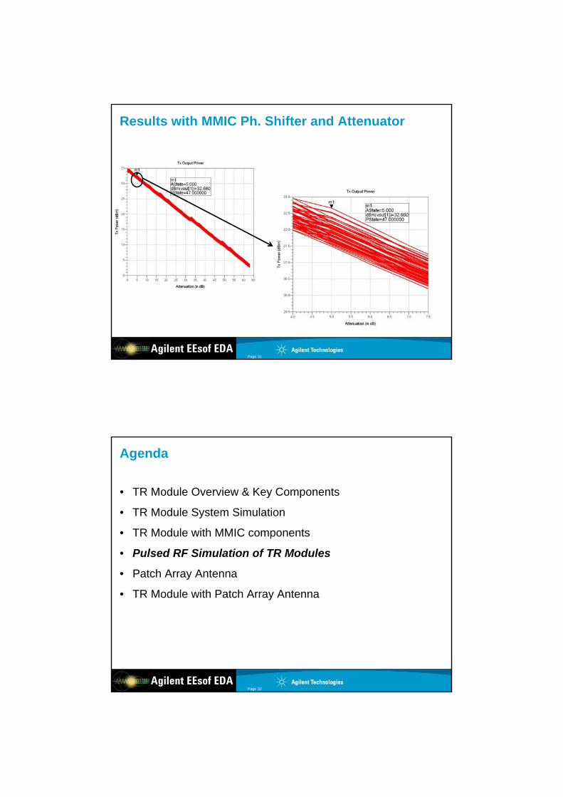
Results with MMIC Ph. Shifter and Attenuator
Page 31
Agilent EEsof EDA
Agenda
• TR Module Overview & Key Components
• TR Module System Simulation
• TR Module with MMIC components
• Pulsed RF Simulation of TR Modules
• Patch Array Antenna
• TR Module with Patch Array Antenna
Page 32

Agilent EEsof EDA
Ptolemy Pulsed-RF TR Module Co-simulation
Page 33
Agilent EEsof EDA
Pulsed RF Response
Page 34

Agilent EEsof EDA
Agenda
• TR Module Overview & Key Components
• TR Module System Simulation
• TR Module with MMIC components
• Pulsed RF Simulation of TR Modules
• Patch Array Antenna
• TR Module with Patch Array Antenna
Page 35
Agilent EEsof EDA
Designing Patch Antenna Array
• Start with a Single Patch
Page 36
Optimized Patch Response
Initial Patch S11 response
Antenna Result Snapshot

Agilent EEsof EDA
Building Patch Array
Page 37
3D View of Antenna Array
Antenna Far Field PatternAntenna Array Snapshot
Agilent EEsof EDA
Cross Coupling in Patch Array Antenna
Page 38

Agilent EEsof EDA
Agenda
• TR Module Overview & Key Components
• TR Module System Simulation
• TR Module with MMIC components
• Pulsed RF Simulation of TR Modules
• Patch Array Antenna
• TR Module with Patch Array Antenna
Page 39
Agilent EEsof EDA
Challenges
• It is essential to combine TR Module system with Antenna Array so that we can characterize the beam steering, loading effect of Antenna on TR Module system etc.
• Challenging part however is to find a way whereby we can integrate Antenna Array (characterized in EM simulator) and TR Module System (or with actual MMIC chips, Circuits etc which is mainly characterized in Schematic domain)
• This is the point where most software would fail and designer won’t be able to combine these 2 important parts of complete system to visualize the complete integrated system performance.
• More often than not designer end-up bringing S-Parameters of designed Antenna thru multi-port Touchstone/S-parameter files and use it as a load to TR Module system (or any other type of systems being designed).
Page 40

Agilent EEsof EDA
ADS Solution
• ADS offers Momentum Far Field Design Kit which can be downloaded freely from Knowledge Center
• This design kit allows designers to integrate Circuit/System level components with part designed in EM environment as a sub-circuit.
• This utility directly launches Radiation Pattern Utility and automatically update amplitude and phase data at each feed points as shown in next slide animation and live demo.
• Another benefit is that there is no manual intervention required from designers side no matter how many feed points are involved in this unique System-Circuit-Antenna co-simulation.
Page 41
Agilent EEsof EDA
Combine TR Module System with Antenna Array
Page 42

Agilent EEsof EDA
Co-simulate TR Module System with Antenna Array
Page 43
Agilent EEsof EDA
Steer the Antenna Beam
Page 44

Agilent EEsof EDA
Further Work
• Non-Linear Amplifier modeling could be easily accomplished by connecting ADS to Agilent Network Analyzers to derive P2D/S2D/X-Parameter models for better non-linear performance prediction and great accuracy in system analysis.
• We could easily replace system level behavioral blocks with Designed Circuits for Bottoms-up verification which will allow us to check designed circuit’s compatibility on a system level design/analysis.
• TR Module Board layout can be done pretty easily in ADS and whole system could be EM co-simulated to take care of layout parasitic which might affect the system performance because of interconnect performance at these high frequencies.
• Performing Board layout EM simulation would also help in predicting some level of EMI issues as well to locate/analyze probable stray radiations.
Page 45
Agilent EEsof EDA
Summary
• ADS provides single software solution to perform System/Circuit/Electromagnetic analysis
• System/Circuit could be integrated with Electromagnetic components such as Antenna array shown in the present case
• ADS cuts work of hours to few seconds and makes it easy to sweep data included in multiple files such as for 6-bit Phase Shifter and Attenuator in the present system whereby it is needed to handle 64 S-parameter file for each components
• Circuit level designs could be placed at the System Level to check for complete system performance along with the Antenna etc and check for some critical parameters such as Beam Steering, phase/amplitude match at various elements etc all in one environment without having to use 3rd party plug-in/sockets etc.
Page 46

专注于微波、射频、天线设计人才的培养 易迪拓培训 网址:http://www.edatop.com
射 频 和 天 线 设 计 培 训 课 程 推 荐
易迪拓培训(www.edatop.com)由数名来自于研发第一线的资深工程师发起成立,致力并专注于微
波、射频、天线设计研发人才的培养;我们于 2006 年整合合并微波 EDA 网(www.mweda.com),现
已发展成为国内最大的微波射频和天线设计人才培养基地,成功推出多套微波射频以及天线设计经典
培训课程和 ADS、HFSS 等专业软件使用培训课程,广受客户好评;并先后与人民邮电出版社、电子
工业出版社合作出版了多本专业图书,帮助数万名工程师提升了专业技术能力。客户遍布中兴通讯、
研通高频、埃威航电、国人通信等多家国内知名公司,以及台湾工业技术研究院、永业科技、全一电
子等多家台湾地区企业。
易迪拓培训课程列表:http://www.edatop.com/peixun/rfe/129.html
射频工程师养成培训课程套装
该套装精选了射频专业基础培训课程、射频仿真设计培训课程和射频电
路测量培训课程三个类别共 30 门视频培训课程和 3 本图书教材;旨在
引领学员全面学习一个射频工程师需要熟悉、理解和掌握的专业知识和
研发设计能力。通过套装的学习,能够让学员完全达到和胜任一个合格
的射频工程师的要求…
课程网址:http://www.edatop.com/peixun/rfe/110.html
ADS 学习培训课程套装
该套装是迄今国内最全面、最权威的 ADS 培训教程,共包含 10 门 ADS
学习培训课程。课程是由具有多年 ADS 使用经验的微波射频与通信系
统设计领域资深专家讲解,并多结合设计实例,由浅入深、详细而又
全面地讲解了 ADS 在微波射频电路设计、通信系统设计和电磁仿真设
计方面的内容。能让您在最短的时间内学会使用 ADS,迅速提升个人技
术能力,把 ADS 真正应用到实际研发工作中去,成为 ADS 设计专家...
课程网址: http://www.edatop.com/peixun/ads/13.html
HFSS 学习培训课程套装
该套课程套装包含了本站全部 HFSS 培训课程,是迄今国内最全面、最
专业的HFSS培训教程套装,可以帮助您从零开始,全面深入学习HFSS
的各项功能和在多个方面的工程应用。购买套装,更可超值赠送 3 个月
免费学习答疑,随时解答您学习过程中遇到的棘手问题,让您的 HFSS
学习更加轻松顺畅…
课程网址:http://www.edatop.com/peixun/hfss/11.html
`

专注于微波、射频、天线设计人才的培养 易迪拓培训 网址:http://www.edatop.com
CST 学习培训课程套装
该培训套装由易迪拓培训联合微波 EDA 网共同推出,是最全面、系统、
专业的 CST 微波工作室培训课程套装,所有课程都由经验丰富的专家授
课,视频教学,可以帮助您从零开始,全面系统地学习 CST 微波工作的
各项功能及其在微波射频、天线设计等领域的设计应用。且购买该套装,
还可超值赠送 3 个月免费学习答疑…
课程网址:http://www.edatop.com/peixun/cst/24.html
HFSS 天线设计培训课程套装
套装包含 6 门视频课程和 1 本图书,课程从基础讲起,内容由浅入深,
理论介绍和实际操作讲解相结合,全面系统的讲解了 HFSS 天线设计的
全过程。是国内最全面、最专业的 HFSS 天线设计课程,可以帮助您快
速学习掌握如何使用 HFSS 设计天线,让天线设计不再难…
课程网址:http://www.edatop.com/peixun/hfss/122.html
13.56MHz NFC/RFID 线圈天线设计培训课程套装
套装包含 4 门视频培训课程,培训将 13.56MHz 线圈天线设计原理和仿
真设计实践相结合,全面系统地讲解了 13.56MHz线圈天线的工作原理、
设计方法、设计考量以及使用 HFSS 和 CST 仿真分析线圈天线的具体
操作,同时还介绍了 13.56MHz 线圈天线匹配电路的设计和调试。通过
该套课程的学习,可以帮助您快速学习掌握 13.56MHz 线圈天线及其匹
配电路的原理、设计和调试…
详情浏览:http://www.edatop.com/peixun/antenna/116.html
我们的课程优势:
※ 成立于 2004 年,10 多年丰富的行业经验,
※ 一直致力并专注于微波射频和天线设计工程师的培养,更了解该行业对人才的要求
※ 经验丰富的一线资深工程师讲授,结合实际工程案例,直观、实用、易学
联系我们:
※ 易迪拓培训官网:http://www.edatop.com
※ 微波 EDA 网:http://www.mweda.com
※ 官方淘宝店:http://shop36920890.taobao.com
专注于微波、射频、天线设计人才的培养
官方网址:http://www.edatop.com 易迪拓培训 淘宝网店:http://shop36920890.taobao.com