a. lai 30/31 jan 2002 dialog cariocacarioca ?. a. lai 30/31 jan 2002 dialog dialog- (nov 2001) has...
TRANSCRIPT

A. Lai 30/31 Jan 2002
DIALOG
CARIOCA
?
A. Lai 30/31 Jan 2002
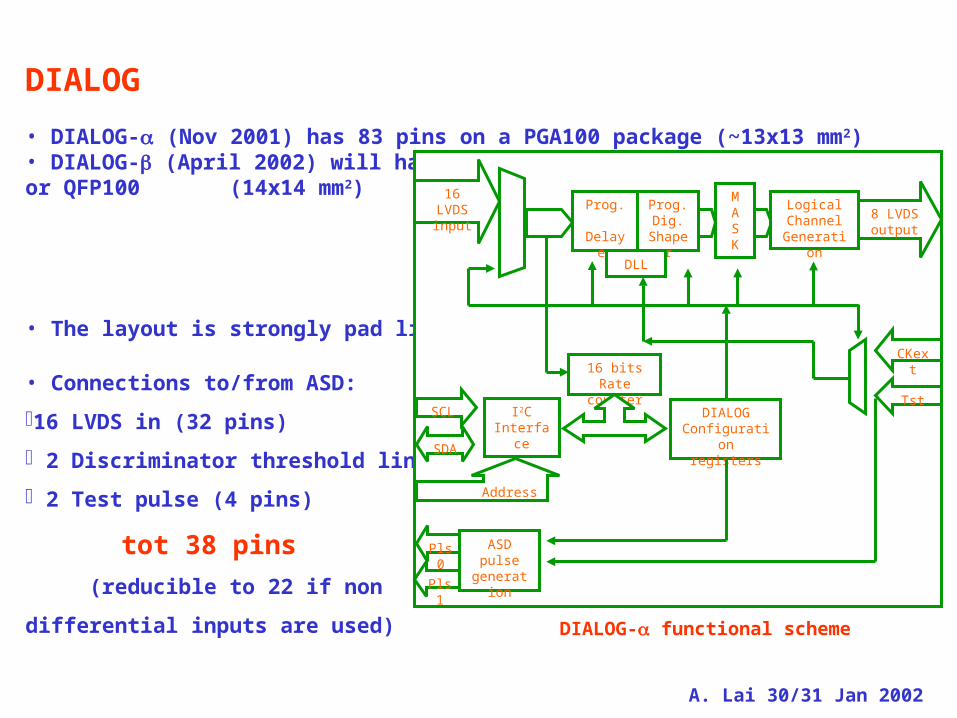
DIALOG
• DIALOG- (Nov 2001) has 83 pins on a PGA100 package (~13x13 mm2)• DIALOG- (April 2002) will have 75 (min) to 91 (max) pins PGA100 or QFP100 (14x14 mm2)
• The layout is strongly pad limited
• Connections to/from ASD:
16 LVDS in (32 pins)
2 Discriminator threshold lines
2 Test pulse (4 pins)
tot 38 pins
(reducible to 22 if non
differential inputs are used)
16 LVDSinput Prog.
Delayer
Prog.Dig.
Shaper
MASK
LogicalChannel
Generation
8 LVDSoutput
I2CInterface
SCL
SDA
DIALOGConfiguration
registers
DLL
Address
16 bitsRate counter
CKext
Tst
Pls0
Pls1
ASD pulse generation
DIALOG- functional scheme

A. Lai 30/31 Jan 2002
DIALOG-CARIOCA
Same board. How to assemble DIALOG and CARIOCA on F/E?- Mechanical integration is not trivial (an additional board will be needed ?!)
Same technology
Integrate the two chips on the same die and put one single IC on front- end ?
+(On top)
(…Otherwise)
A. Lai 30/31 Jan 2002
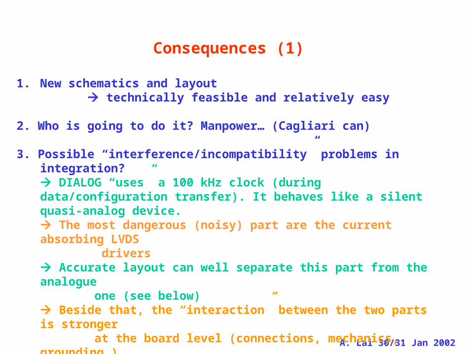
Consequences (1)
1. New schematics and layout technically feasible and relatively easy
2. Who is going to do it? Manpower… (Cagliari can)
3. Possible “interference/incompatibility” problems in integration? DIALOG “uses” a 100 kHz clock (during data/configuration transfer). It behaves like a silent quasi-analog device. The most dangerous (noisy) part are the current absorbing LVDS
drivers Accurate layout can well separate this part from the analogue
one (see below) Beside that, the “interaction” between the two parts is stronger
at the board level (connections, mechanics, grounding…)

A. Lai 30/31 Jan 2002
Layout issues
250 m
Std cells area: squeezable at least to 50%
data
path
data
path
Inp
ut
sig
nals
Inp
ut s
ign
als
Outputs (logical channels)
controls

A. Lai 30/31 Jan 2002
262 m
61
m
290 m
290 m
20
00
m
25
0
m
Sizes of full custom cells
Calibration DLL
Prog. Delay, Digital Shaper and 1st stage of logics (1 channel)
Pro
g.
Dela
y,
Dig
ital S
hap
er
an
d 1
st sta
ge o
f lo
gic
s (
8 c
han
nels
)
A. Lai 30/31 Jan 2002
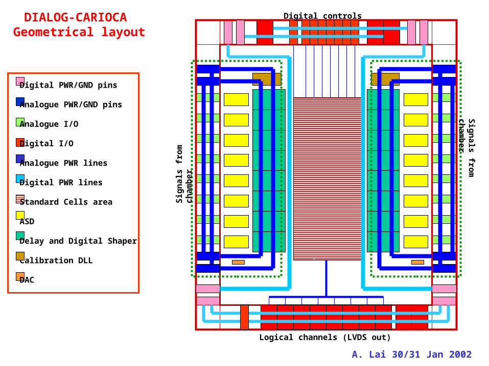
DIALOG-CARIOCA Geometrical layout
Digital PWR/GND pins
Analogue PWR/GND pins
Analogue I/O
Digital I/O
Analogue PWR lines
Digital PWR lines
Standard Cells area
ASD
Delay and Digital Shaper
Calibration DLL
DAC
Sig
nals
fro
m
ch
am
ber
Sig
nals
from
ch
am
ber
Logical channels (LVDS out)
Digital controls
A. Lai 30/31 Jan 2002
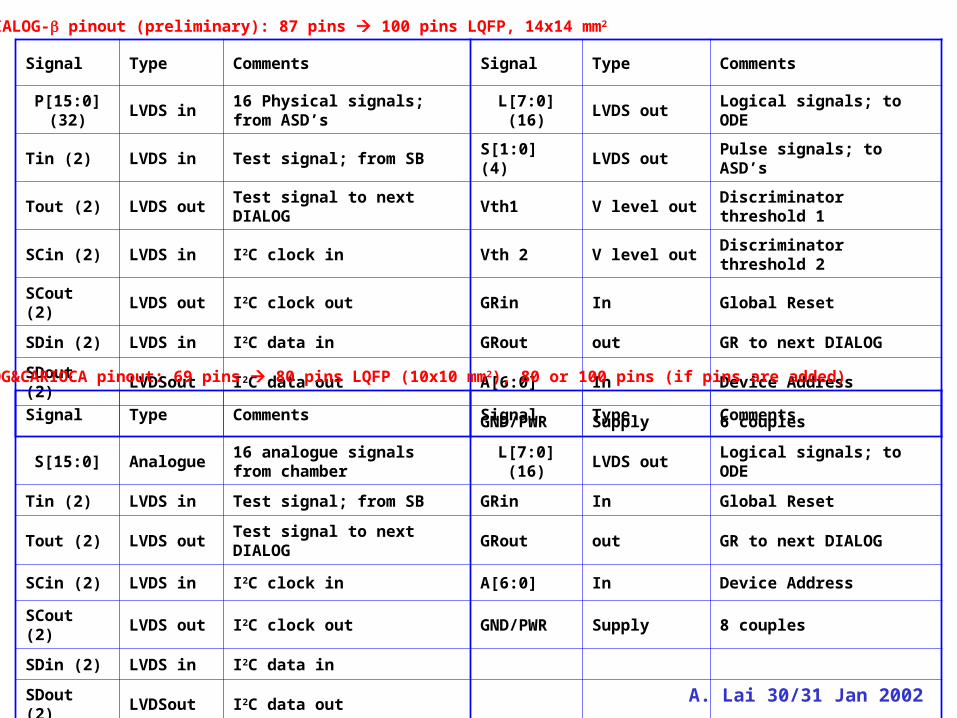
Signal Type Comments Signal Type Comments
P[15:0] (32)
LVDS in16 Physical signals; from ASD’s
L[7:0] (16)
LVDS out Logical signals; to ODE
Tin (2) LVDS in Test signal; from SB S[1:0] (4) LVDS out Pulse signals; to ASD’s
Tout (2) LVDS outTest signal to next DIALOG
Vth1 V level outDiscriminator threshold 1
SCin (2) LVDS in I2C clock in Vth 2 V level outDiscriminator threshold 2
SCout (2) LVDS out I2C clock out GRin In Global Reset
SDin (2) LVDS in I2C data in GRout out GR to next DIALOG
SDout (2)
LVDSout I2C data out A[6:0] In Device Address
GND/PWR Supply 6 couplesDIALOG&CARIOCA pinout: 69 pins 80 pins LQFP (10x10 mm2), 80 or 100 pins (if pins are added)
DIALOG- pinout (preliminary): 87 pins 100 pins LQFP, 14x14 mm2
Signal Type Comments Signal Type Comments
S[15:0] Analogue16 analogue signals from chamber
L[7:0] (16)
LVDS out Logical signals; to ODE
Tin (2) LVDS in Test signal; from SB GRin In Global Reset
Tout (2) LVDS outTest signal to next DIALOG
GRout out GR to next DIALOG
SCin (2) LVDS in I2C clock in A[6:0] In Device Address
SCout (2) LVDS out I2C clock out GND/PWR Supply 8 couples
SDin (2) LVDS in I2C data in
SDout (2)
LVDSout I2C data out

A. Lai 30/31 Jan 2002
Fro
m c
ham
ber
FRONT-END BOARDS (my present envisaging)
F/E boards inside chamber (not visible in reality)
Chamber cage Connectors are accessible from outside
DIALOGCARIOCA
Logical channels out
Controls out
Controls inPWR/GND
Logical channels out
Controls out
Controls inPWR/GND
DIALOG – CARIOCA (separated)
Interboard connections
?

A. Lai 30/31 Jan 2002
Consequences (2)
4. Additional time in the schedule. What is the present schedule?
Chamber production starts beginning of 2003
The electronics to be used in the tests of produced chambers will not be the definitive one. Only the ASD chips will be used.
This disentangles the front-end production schedule from the chamber production one.
Proposal:
Produce and test accurately both the final version of CARIOCA and DIALOG within 2002 (see “full chain test”).
Prepare and submit the CARIOCA_DIALOG integrated version beginning of 2003.
Test, compare and approve/discard it within half 2003.

A. Lai 30/31 Jan 2002
Consequences (3)
5. Impact on the system: The front-end design is simplified… but:
We have MANY font-ends:
• Positive
• Negative
• RPC?
• GEM?
Moreover: also a standalone CARIOCA (and DIALOG) version is needed
How about RPC and GEM? Can they use the same chip as the MWPC? (This should be answered quickly…)
Yes: 2 kinds of D-C chip are needed: DC+, DC-.
No: 3 kinds: DC+, DC-, D/C standalone
Still worthwhile ? We think yes:
The cost is invariant with the number of project per wafer.
DIALOG and CARIOCA will be developed and tested separately in any case

A. Lai 30/31 Jan 2002
Consequences (4)
Which name?
SuperDIALOG ?
CARIOCAgliari ?
SuperD ?
A committee, a competition and a prize to solve this fundamental problem…

A. Lai 30/31 Jan 2002
Conclusions
• The CARIOCA-DIALOG integration is appealing from the system point of view and technically feasible.
• The impact on the Muon Project schedule can be minimized
• Differences with the standalone solution: On board connections, mechanics, grounding are better; Interaction with the LVDS drivers can be kept under control; Final answer can be given only by tests; • The different kind of front-ends in the system are not a serious problem (the system cost is unaffected, the additional work is acceptable)
A try is feasible and worthwhile
The final decision could be postponed to the 1st half of 2003, butthe final versions of both CARIOCA and DIALOG should be realized with an eye to their integration (especially from the layout point of view).