active integrated antennas for sensor and … · technischen universität münchen ... first and...
TRANSCRIPT

Active Integrated Antennas for Sensor and Communication Applications
Martin Kaleja

Fachgebiet Höchstfrequenztechnik an der Technischen Universität München
Active Integrated Antennas for Sensor and Communication Applications
Martin Kaleja
Vollständiger Abdruck der von der Fakultät für Elektrotechnik und Informationstechnik der Technischen Universität München zur Erlangung des akademischen Grades eines
Doktor – Ingenieurs genehmigten Dissertation. Vorsitzender: Univ.-Prof. Dr.-Ing. U. Wagner Prüfer der Dissertation: 1. Univ.-Prof. Dr.-Ing., Dr.-Ing. habil. E. Biebl 2. Prof. Dr. Z. Popovic, Univ. of Colorado / USA Die Dissertation wurde am 25.04.2001 bei der Technischen Universität München eingereicht und durch die Fakultät für Elektrotechnik und Informationstechnik am 31.07.2001 angenommen.

Abstract in Deutsch
Zur Frequenzerzeugung und Abstrahlung werden im Millimeterwellenbereich aktive integrierte Antennen eingesetzt. Sie eignen sich aufgrund ihrer Eigenschaften wie kompakte Bauform bei 24 GHz und günstige Herstellungskosten für verschiedene Kommunikations- und Sensoranwendungen. Durch die Kombination von Antennen- / Oszillatoreigenschaften ist die Modellierung dieser Antennen sehr schwierig. In dieser Arbeit werden Modellierungsansätze für verschiedene Antennenkonzepte vorgestellt, die den Entwurf wesentlich vereinfachen während die Entwurfsgenauigkeit erhalten bleibt. Die Gültigkeit dieser Modellierungen wird durch Messungen bestätigt. Die Realisierung von neuartigen Anwendungsmöglichkeiten für diese Antennen schließt diese Arbeit ab.
Abstract in English Active integrated antennas are used for frequency generation and the radiation of millimeter-waves. Due to their compactness and low-cost fabrication, they are suited for different sensor and communication applications. Modeling these antennas is a difficult task due to the com-bination of antenna and oscillator properties. This thesis presents modeling approaches for different antenna concepts that significantly ease the design process while maintaining design accuracy. The validity of these approaches is proved with measurements. The thesis closes with examples for the realization of new applications for these antennas.

ACKNOWLEDGEMENT
This doctoral thesis would have never been possible without the support of a number of people and organizations.
First and foremost I would like to thank my thesis advisor Prof. Dr. Erwin Biebl who showed unwavering support in both my academic and professional pursuits. His office door was always open for any kind of problem throughout the work.
I would also like to thank Prof. Dr. Zoya Popovic from the University of Colorado who made it possible for me to work in her group on some parts of my thesis. She always had the right refer-ence for my questions. I am also glad that she agreed to become the co-advisor of my work.
I want to thank Prof. Peter Russer for the access to the equipment at the Lehrstuhl für Hochfre-quenztechnik.
I am indebted to the Hanns-Seidel-Stiftung and the Technische Universität München for grant-ing me a scholarship, and the IEEE MTT society for granting me two fellowships. Without this financial support, I would not have been able to work on this thesis.
During my work, I could always count on the support from my colleagues. That is why my spe-cial thanks go to Arnold Herb, Dr. Ralph Rasshofer, Dr. Franz Sinnesbichler, and Dr. Gerhard Friedsam at the Technische Universität München, and Manoja Weiss, Dr. Stefania Romisch, Jan Peeters Weem, Dr. Michael Forman, Dr. Jim Vian, Joe Haggerty, and Dr. Todd Marshall from the University of Colorado.
Writing their diploma thesis or student project as part of my research, Arnold Herb, Erich Gras-berger, Alexander Grübl, and Peter Vrzal made this work a success.
I want to thank Astrid Habel and Andrea Holm for processing the thin-film substrates; the me-chanics workshop with Manfred Fuchs, Josef Franzisi, and Manfred Agerer for solving all my mechanical problems; and Rachel Tearle for dealing with the administration at CU.
Regarding the realized applications, many companies supported my research with free samples and financial support, especially Dr. Luy from the DaimlerChrysler Research Center and Dr. Pitschi from Spinner. Heinrich Siebert from Spinner gave me valuable insight in his knowledge.
I would like to mention the support and encouragement of my parents throughout the years of my academic education, which culminate in this thesis.
I would especially like to thank my partner Sabine Knauf for her understanding and moral sup-port the whole time during this work.
München, April 2001

I
TABLE OF CONTENTS
1 Introduction 1 1.1 State of the Art of Active Integrated Antennas........................................................1
1.1.1 Historical Background .................................................................................1
1.1.2 Antenna Configurations ...............................................................................2
1.1.2.1 Active Devices.............................................................................2
1.1.2.2 Antenna Elements........................................................................2
1.1.3 Frequency Tunable Active Integrated Antennas..........................................3
1.1.4 Dielectric Stabilized Active Integrated Antennas ........................................4
1.1.5 Injection Locked Active Integrated Antennas..............................................4
1.1.6 Active Integrated Antenna Arrays ...............................................................4
1.2 Applications of Active Integrated Antennas, State of the Art .................................5
1.2.1 Automotive Applications .............................................................................6
1.2.2 Sensor Applications (Non-Automotive) ......................................................6
1.2.3 Communication/Tagging Applications ........................................................6
1.3 Overview..................................................................................................................8
2 Oscillator Theory Applied to Active Integrated Antennas 10 2.1 Linear Theory.........................................................................................................11
2.1.1 Derivation of Linear Oscillation Condition ...............................................11
2.1.2 Stability Analysis Using Linear Oscillator Theory....................................13
2.2 Nonlinear Theory ...................................................................................................14
2.2.1 Nonlinear Oscillator Model Based on Kurokawa ......................................14
2.2.2 Theory of Harmonic Balance Nonlinear Analysis .....................................17
2.2.3 Implementation of Harmonic Balance Analysis in Commercial Software 19
2.3 Comparison of Oscillator Theories for AIAs.........................................................19
2.3.1 Application of Linear Oscillator Theory....................................................19
2.3.2 Derivation of the Steady-State ...................................................................20
2.3.3 Linear Oscillator Design Using Reduced S-Parameters ............................21
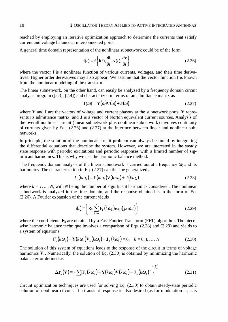
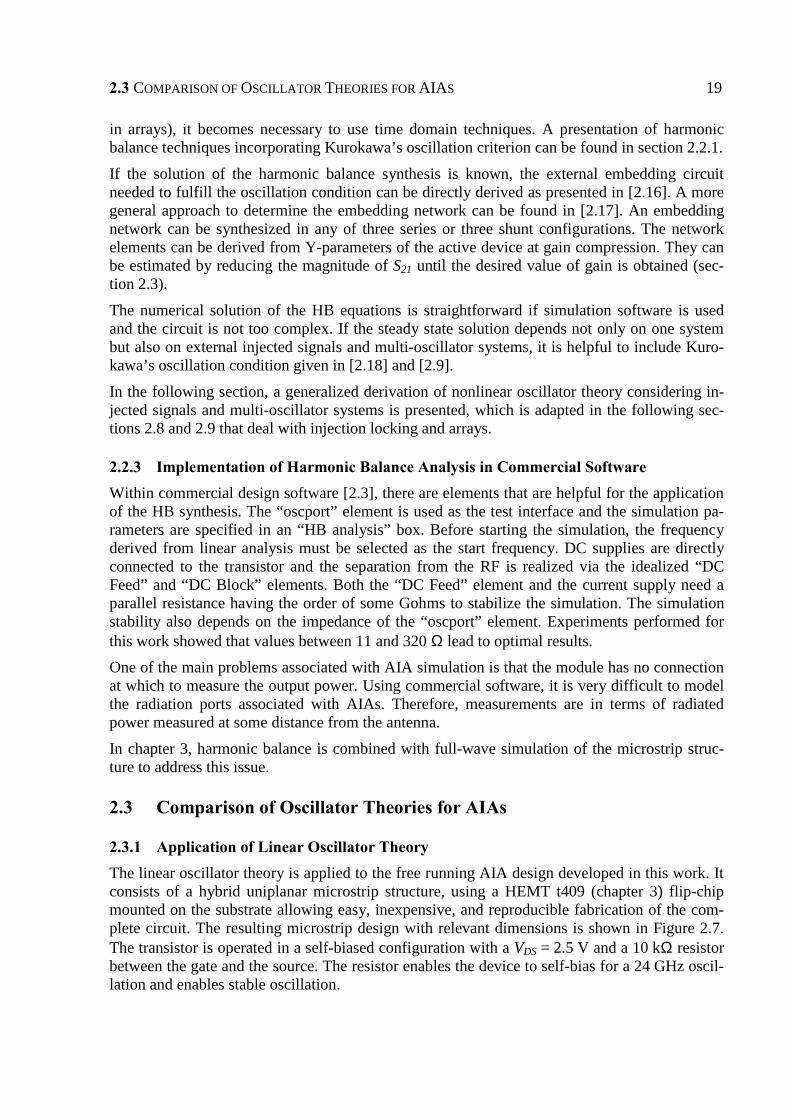
2.3.4 Kurokawa’s Oscillation Condition with Reduced S-Parameters ...............22
2.3.5 Numerical Solution of the Oscillation Condition.......................................23

II
2.4 Frequency Tunable Active Integrated Antennas ................................................... 24
2.4.1 Background of VCOs ................................................................................ 24
2.4.2 Frequency Tunable AIA Design................................................................ 24
2.5 Phase Noise ........................................................................................................... 26
2.5.1 Definitions ................................................................................................. 27
2.5.2 Phase Noise in AIAs.................................................................................. 29
2.5.3 Phase Noise in Coupled AIAs ................................................................... 31
2.6 Q-Factor................................................................................................................. 33
2.6.1 Definitions of Q-Factors............................................................................ 33
2.6.1.1 Unloaded Q-Factor.................................................................... 33
2.6.1.2 Loaded and External Q-Factors ................................................ 34
2.6.2 Influence of Various Loss Contributions on the Q-Factor ........................ 34
2.6.3 Determination of the Q-Factor .................................................................. 37
2.6.4 Different Resonator Shapes for AIAs........................................................ 39
2.7 Dielectric Stabilized Active Integrated Antennas ................................................. 40
2.7.1 Dielectric Resonator Modes ...................................................................... 40
2.7.2 Dielectric Resonator Coupling .................................................................. 41
2.7.2.1 Serial Coupling ......................................................................... 41
2.7.2.2 Parallel Coupling ...................................................................... 42
2.7.3 DR Stabilized Active Integrated Antenna Design..................................... 44
2.8 Injection Locking .................................................................................................. 46
2.8.1 Definition................................................................................................... 46
2.8.2 Injection Locked AIA................................................................................ 48
2.9 Coupling and Power Combining ........................................................................... 48
2.9.1 Coupling Topologies ................................................................................. 49
2.9.2 Radiative Coupling Mechanisms............................................................... 49
2.9.3 AIA Model for Coupling Modeling .......................................................... 49
2.9.4 Radiative Coupling Modeling ................................................................... 50
2.9.5 Coupling Theory........................................................................................ 51
2.9.6 Theory Applied to the Free Running AIA Array ...................................... 53
2.9.7 Power Combining Methods....................................................................... 55
2.9.8 Spatial Power Combining.......................................................................... 55

III
3 Circuit and Device Models and Their Implementation for AIA Design 57 3.1 Semiconductor Devices for Integrated Antennas ..................................................57
3.1.1 Two-Terminal Devices...............................................................................57
3.1.2 IMPATT Diodes ........................................................................................58
3.1.3 Three-Terminal Devices.............................................................................58
3.1.3.1 High Electron Mobility Transistors...........................................59
3.1.3.2 Heterojunction Bipolar Transistors ...........................................59
3.2 Transistor Modeling for Active Integrated Antennas ............................................60
3.2.1 S-Parameter Description ............................................................................60
3.2.2 Large-Signal Modeling ..............................................................................63
3.3 Circuit Simulation Methods...................................................................................64
3.3.1 Equivalent Circuits for the Microstrip Lines .............................................64
3.3.2 Equivalent Circuits for Microstrip Antennas/Resonators ..........................65
3.4 Full Wave Analysis in the Frequency Domain ......................................................66
3.4.1 Integral Equation Formulation ...................................................................66
3.4.2 Determination of the Green’s Functions ....................................................67
3.4.3 Method of Moments...................................................................................68
3.4.4 Calculation of the Impedance Matrix.........................................................70
3.4.5 Calculation of the Input Impedance ...........................................................70
3.4.6 Implementation of the Full-Wave Analysis in “Momentum”....................70
3.5 Comparison of Circuit and Field Simulation .........................................................71
3.5.1 Microstrip Patch Simulation ......................................................................71
3.5.2 AIA Simulation ..........................................................................................72
3.5.3 Results ........................................................................................................74
3.5.3.1 Accuracy....................................................................................74
3.5.3.2 Execution Time..........................................................................75
3.5.4 Conclusion .................................................................................................75
3.6 Calculation of the Antenna Parameters..................................................................75
3.6.1 Radiation Pattern........................................................................................75
3.6.1.1 Single AIA.................................................................................75
3.6.1.2 AIA Array..................................................................................76
3.6.2 Polarization ................................................................................................76
3.6.3 Radiated Power ..........................................................................................77
3.6.4 Gain ............................................................................................................77

IV
3.6.5 DC to RF Conversion Efficiency .............................................................. 78
3.6.6 Visualization.............................................................................................. 78
3.6.7 Estimation of the Main Radiating Patch.................................................... 78
4 Experimental Validation of the AIA Designs 79 4.1 Measuring AIAs .................................................................................................... 79
4.1.1 Frequency and Output Power .................................................................... 79
4.1.2 Q-Factor and Phase Noise ......................................................................... 79
4.1.2.1 Methods..................................................................................... 79
4.1.2.2 Direct Spectrum Method........................................................... 80
4.1.2.3 Application of the Direct Spectrum Method............................. 80
4.1.2.4 Deriving the Q-Factor from the Phase Noise Measurements ... 80
4.1.3 Radiation Behavior .................................................................................... 81
4.2 Single Free-Running AIA ..................................................................................... 82
4.2.1 Bias Effects on Output Frequency and Power........................................... 83
4.2.2 Self Mixing Behavior ................................................................................ 84
4.2.3 Q-Factor and Phase Noise ......................................................................... 85
4.2.4 Radiation Behavior .................................................................................... 87
4.2.5 Effective Radiated Power, Antenna Gain, and Conversion Efficiency..... 89
4.3 Frequency Tunable AIA........................................................................................ 90
4.3.1 Tuning Range ............................................................................................ 91
4.3.2 Phase Noise ............................................................................................... 93
4.3.3 Radiation Behavior .................................................................................... 93
4.4 Injection-Locked AIA ........................................................................................... 94
4.4.1 Locking Range........................................................................................... 95
4.4.2 Phase Noise ............................................................................................... 96
4.4.3 Radiation Behavior .................................................................................... 97
4.5 AIA Array.............................................................................................................. 98
4.5.1 Coupling Behavior..................................................................................... 98
4.5.2 Phase Noise ............................................................................................... 99
4.5.3 Radiation Behavior .................................................................................... 99
5 Sensor and Communication Applications 102 5.1 RFID System ....................................................................................................... 103

V
5.1.1 The Active Transmitter “Tag” .................................................................103
5.1.1.1 The RF Front-End....................................................................103
5.1.1.2 The Code Generator.................................................................104
5.1.1.3 The Power Supply ...................................................................104
5.1.2 The Imaging Receiver ..............................................................................105
5.1.2.1 The Lens for Quasi-Optical Beamforming..............................105
5.1.2.2 The Detector ............................................................................105
5.1.2.3 The Detector Array..................................................................106
5.1.2.4 The Analog Signal Processing.................................................107
5.1.2.5 The Digital Signal Processing .................................................107
5.1.3 Visualization ............................................................................................108
5.1.4 System Data .............................................................................................110
5.1.5 Presentation of the System.......................................................................111
5.1.6 Possible Improvements ............................................................................111
5.2 Crash Sensor ........................................................................................................112
5.2.1 Structure of the Crash Sensor...................................................................112
5.2.1.1 IMPATT Based AIA ...............................................................112
5.2.1.2 HEMT Based AIA ...................................................................113
5.2.2 Principle of Operation ..............................................................................113
5.2.3 Crash Tests ...............................................................................................114
5.2.4 Discussion ................................................................................................116
6 Conclusion 117
A Appendix 121 A.1 Fabrication ...........................................................................................................121
A.2 Substrate Parameters ............................................................................................121
A.3 Dielectric Resonator Parameters..........................................................................122
References Chapter 1 123
References Chapter 2 129
References Chapter 3 134
References Chapter 4 - A 136


1 INTRODUCTION Active integrated antennas (AIAs) combine prominent features that make them usable for both military and commercial applications. The most important feature is that the antenna and the active device are treated as a single entity, allowing compactness, low cost, low profile, mini-mum power consumption, and multiple functionality.
A typical AIA consists of one or more active devices such as diodes (Gunn, IMPATT, Schot-tky, and varactor) and/or three terminal devices (MESFET, HEMT, or HBT) integrated with planar antennas such as printed dipoles, microstrip patches, bowties, or slot antennas. To realize different functionalities, AIAs can be made frequency tunable, injection locked, or mutually coupled. Choosing the adequate configuration, multiple communication and sensor applications can be realized. This thesis presents theoretical and experimental work, which advances the state of the art in active integrated antennas for microwave and millimeter-wave applications.
In this chapter, the state of the art in AIAs is presented starting from the history to actual pub-lished works. It also gives an overview of this thesis.
1.1 State of the Art of Active Integrated Antennas
1.1.1 Historical Background Hertz already introduced the concept of an active antenna with his end-loaded dipole transmit-ter and resonant square-loop antenna receiver [1.1]. However, neither the transmitter nor the receiver used any matching networks between the circuit and the antenna terminals. This status quo remained for nearly three decades, until the integrated antenna concept surfaced again in the early- and mid-1960s. Using a tunnel diode, Copeland and Robertson demonstrated a mixer-integrated antenna, which they describe as an “antennaverter”. They also used a traveling wave antenna, together with tunnel diodes, to operate as a traveling wave amplifier, which they called an “antennafier” [1.2]. Meinke and Landstorfer described the integration of a FET transistor to the terminals of a dipole to serve as a VHF amplifier for reception at 700 MHz [1.3]. Following their work, Ramsdale and Maclean used BJTs and dipoles for transmission applications in 1971 [1.4]. What is generally accepted as the first modern active antenna, was developed and pub-lished by Thomas et al. in February 1985. It was a Gunn integrated rectangular microstrip patch antenna operating at X-band frequencies [1.5].
In 1974, an array of injection locked active antennas was demonstrated to perform phase shifterless beam steering [1.6] and a variety of other functionalities for AIA arrays have been demonstrated.
Active antennas have found use as elements of large-scale spatial power combiners in which the radiation of many AIAs combines coherently. A variety of such combiners has been demon-strated at microwave and millimeter-wave frequencies [1.7] with 120 watt power levels at X-band [1.8] and watt level at Ka-band [1.9].

2 1 INTRODUCTION
1.1.2 Antenna Configurations
1.1.2.1 Active Devices
Two-terminal devices, e.g. IMPATT diodes [1.10], [1.11], [1.12], [1.13] and Gunn diodes [1.5], [1.14], as well as three-terminal devices, e.g. MESFETs [1.15], [1.16] [1.17], HEMTs [1.18] and HBTs [1.19], [1.20], can be used as the active sources. In this work, HEMTs [1.21] and HBTs [1.22] are used. The early development of active integrated antennas at microwave and millimeter-wave frequencies concentrated first on two-terminal devices and then moved to three-terminal devices [1.23]. Two-terminal devices are suitable for high power applications at millimeter-wave frequencies, but have the disadvantage of low DC-to-RF efficiency. Three-terminal devices, on the other hand, have the advantage of high DC-to-RF efficiency but are limited by the lower cutoff frequencies. Three-terminal devices have another advantage of easy integration with planar circuit structure, in either a hybrid or monolithic approach.
1.1.2.2 Antenna Elements
Recent research in active antennas has mainly concentrated on microstrip patch types [1.1], [1.5], [1.23], [1.24], [1.25], [1.26], where solid-state devices (usually diodes or FETs) are inte-grated with microstrip patches resulting in convenient planar, low-cost radiating elements. They are not only the output loads of oscillators but serve also as resonators, determining the oscilla-tion frequency. The input impedance of the antenna element is therefore an important informa-tion for designing AIAs. Besides the oscillator type AIA, where the active device functions as the oscillator with a passive radiating element at the output port, the amplifier type AIA is also reported. In this case, the active device works as an amplifier with passive antenna elements at the input or output port [1.27]. When antenna elements are integrated at input and output ports, the circuit becomes a quasi-optical amplifier [1.28]. The integration of amplifiers in passive antenna structures increases the antenna gain and bandwidth and improves the noise perform-ance.
Active microstrip patch oscillator antennas suffer from narrow bias tuning ranges and large output power variations that can be improved by using varactors connected to the radiating ele-ments.
The majority of active microstrip antennas exhibits limited tuning ranges, high cross-polarization levels, and large output power variations. At millimeter-wave frequencies, small patch antenna dimensions cause difficulties during device integration. DC bias lines also cause problems and degrade the performance. There are alternative configurations to the microstrip patch. Each has its pros and cons when applied to AIAs:
• The notch antenna is the planar equivalent to a waveguide horn, and it is capable of very broad impedance bandwidths. Since the notch antenna uses a slotline feed, it is ideal for integration with two terminal devices.
• A planar broadside radiator can also be constructed from a resonant slotline. There are several configurations such as slotline dipoles, loops, or rings. Unlike a microstrip patch, the antenna is a bi-directional radiator, which can be used with polarizers in spa-tial amplifier applications [1.29], [1.7]. In 1993, Kawasaki and Itoh developed a micro-strip FET oscillator using a slot antenna [1.30]. Kormanyos, Katehi, and Rebeiz pub-lished in 1994 a CPW-fed active slot antenna [1.31]. Active slotline antennas integrated with an IMPATT diode were investigated by Luy and Biebl in 1993 [1.12].
1.1 STATE OF THE ART OF ACTIVE INTEGRATED ANTENNAS 3
• The inverted microstrip patch is attractive for integrated antennas because it offers two distinct advantages [1.14], [1.32], [1.33]. First, diode or probe insertion does not require drilling through the substrate as in microstrip. This characteristic allows non-destructive device testing and position optimization in inverted microstrip. Second, the inverted substrate can serve as a built-in radome for protection.
1.1.3 Frequency Tunable Active Integrated Antennas For some applications, it may be useful to vary the oscillation frequency of the AIA. Since the ISM (Industrial, Scientific, and Medical) bandwidth at 24 GHz is restricted to 250 MHz, post-production adjustment is used to compensate for parameter variations of the active device, the low Q-factor as well as the narrow bandwidth of the microstrip lines, and processing nonuni-formities. Additionally, VCOs are used in FM-CW radar systems (section 1.2.1), and AIAs with wide tuning ranges can be used for array beam scanning methods [1.34], [1.35].
The most common VCO design uses a varactor diode as the reactive tuning element. The volt-age dependence of the junction capacitance is used to change the electrical length of the resona-tor. Bhartia and Bahl [1.36] describe the use of varactor diodes in microstrip patches as a means of changing the resonance frequency. Navarro et al. [1.37] portray an active notch antenna, tuned by a varactor diode, in which the source oscillator is a Gunn diode. Kitchen [1.38] depicts varactor diode tuning applied to transistor oscillators in which the devices are located in the gate and source circuits, and a microstrip load appears in the drain circuit. A possibility to im-prove the tuning range of a VCO is presented by Chang and York [1.39] by using a feedback amplifier.
However, these circuits appear to function as wide bandwidth oscillators rather than active an-tennas. It is more complicated to tune an active antenna since the radiation pattern is influenced by the diode and the antenna can exhibit several resonances. Haskins et al. [1.40] developed an active patch antenna with a tuning range of 100 MHz that is 4.4% of the nominal operation fre-quency with good radiation patterns over the tuning bandwidth. A transistor-based AIA com-bined with a varactor is described in this work (compare [1.41]). To solve the problem of mode hopping, a feedback oscillator topology where the patch antenna, placed in the feedback path of an amplifier circuit, acts as the sole frequency selecting structure. The amplifier bandwidth is selected to eliminate the possibility of multi-moding [1.42].
A typical problem is to design the VCO circuit such that f is a linear function of bias voltage within given tolerances. This can be achieved using a special hyperabrupt diode or shaping the tuning voltage function of an abrupt diode. Additionally, another nonlinear element can be used to convert a tuning voltage to a nonlinear control voltage [1.43].
Frequency variations can also be realized with bias tuning of the transistor. This method is use-ful if very small frequency shifts are required since the output power also depends very strongly on the bias. York et al. [1.44] describe an antenna with a tuning range of 250 MHz that is 3% of its nominal operation frequency of 8 GHz by changing the bias voltage applied to the transistor. Comparing diode and transistor tuning [1.40] shows that the transistor tuning range is half that obtained with the diode and the output power varies by more than 20 dB compared to 4 dB with diode tuning.
4 1 INTRODUCTION
1.1.4 Dielectric Stabilized Active Integrated Antennas Stabilized microwave oscillators using FETs have been reported by many authors. James et al. obtained stabilized GaAs FET oscillators in an 11 GHz band using a resonant cavity as either a transmission filter or an external feedback circuit [1.45]. Using a cavity as the resonant circuit makes the oscillator or antenna circuit more complicated and hard to manufacture. Three di-mensional production techniques must be applied, resulting in an expensive structure. A com-promise between a cavity on the one hand, and a non-stabilized oscillator on the other hand, can be found using a dielectric resonator (DR). The main advantages of a DR are its small size and low-price. The DR can be easily integrated with the uniplanar circuit by placing it on the sub-strate. Oscillators stabilized with a DR (DROs) can be divided into two groups. The DR is used as a band rejection filter (DR coupled to a single line) or as an external feedback device (DR placed between two lines). A stabilized GaAs FET oscillator using a dielectric resonator as a band rejection filter was reported by Abe et al. at 6 GHz [1.46] and by Sun and Wei at X-band frequency [1.47].
Some oscillators based on a DR as a feedback element were also reported: Loboda et al. [1.48] present a DRO at 2 GHz based on a silicon bipolar transistor amplifier. Saito et al. developed oscillators using GaAs FETs at 6 GHz [1.49] and Ishihara et al. at 9-14 GHz [1.50]. To allow application of a DR stabilized oscillator in a PLL, Lee and Day developed a DRO combined with a varactor diode at X-band leading to a tuning range of 0.2% [1.51].
Combination of DRs together with AIAs can hardly be found. The reason for this is that the DR influences the radiated field of the AIA considerably. This effect can be exploited if the DR is used as the frequency determining and radiating element. A DR and an active bipolar junction transistor were integrated to operate as a stable radiating DRO at 500 MHz, and a Gunn inte-grated dielectric resonator antenna was demonstrated at 5.55 GHz [1.1].
1.1.5 Injection Locked Active Integrated Antennas To improve the AIA properties, external signals can be use to injection lock AIAs. With a sin-gle injection locked AIA, a maximum of 180° phase shift is theoretically possible. However, by using two sequentially rotated antennas, nearly 360° phase shift can be obtained [1.52]. These observations indicate that the injection locked AIA may form the basis for a beam-steered ar-ray. However, due to the dependence of the free-running AIA on device bias, these elements can be frequency swept by DC bias perturbation. Therefore, a class of direct phase shift keying AIAs can be developed [1.53]. This type of antenna can be applied in a short-haul, low cost communication link [1.54].
1.1.6 Active Integrated Antenna Arrays Originally, the concept of quasi-optical power combining was proposed to combine the output power from an array of many solid-state devices in free-space to overcome the power limita-tions of individual devices at millimeter-wave frequencies [1.55]. In fact, the development of novel quasi-optical power combiners has been one of the main driving forces for the research on AIAs during the past ten years [1.7]. There are two ways to arrange multiple active antennas. Loosely coupled AIAs are arranged in arrays with a period of at least λ/2, whereas strongly coupled AIAs, with periods on the order of λ/10, are referred to as grids. In arrays, mutual cou-pling is small and each element approximately behaves the same when out of the array.
Many innovative approaches have been proposed for realizing efficient quasi-optical power-combining arrays. Among them were beam arrays, grid arrays [1.15], patch based arrays [1.56], [1.57], [1.58], slot-based arrays [1.30], [1.59] and monopole probed based arrays. Bi-directional
1.2 APPLICATIONS OF ACTIVE INTEGRATED ANTENNAS, STATE OF THE ART 5
amplifier arrays with both transmitting and receiving capabilities have also been demonstrated [1.29]. A second harmonic patch antenna Gunn diode combiner showed a 10.2% isotropic con-version efficiency at 18.6 GHz [1.60]. A 5 × 5 array of MESFET oscillators was combined in a planar Fabry-Perot cavity at 10 GHz with an ERP of 20.7 watts and a directivity of 16.4 dB [1.61]. The largest number of devices combined so far was in a planar grid oscillator in which the individual output powers were combined in free space. This grid oscillator, which operated at 5 GHz, contained 100 MESFETs [1.15], and similar oscillators using 36 devices were built at C-, Ku-and Ka-bands [1.62], [1.63].
For a beam steering power combining array, varactor-tuned active antennas with wide tuning ranges are used to control the phase distribution in the array and to keep minimal power varia-tion over the collective locking range of the active elements. Several other wideband varactor tuned arrays have also been developed using varactor tunable notch antennas and tunable power combiners [1.37] and quasi-optical grid VCOs consisting of two active grids [1.64].
The active planar structure is versatile in that different components may be designed separately and then combined into one overall system by stacking the two-dimensional grids.
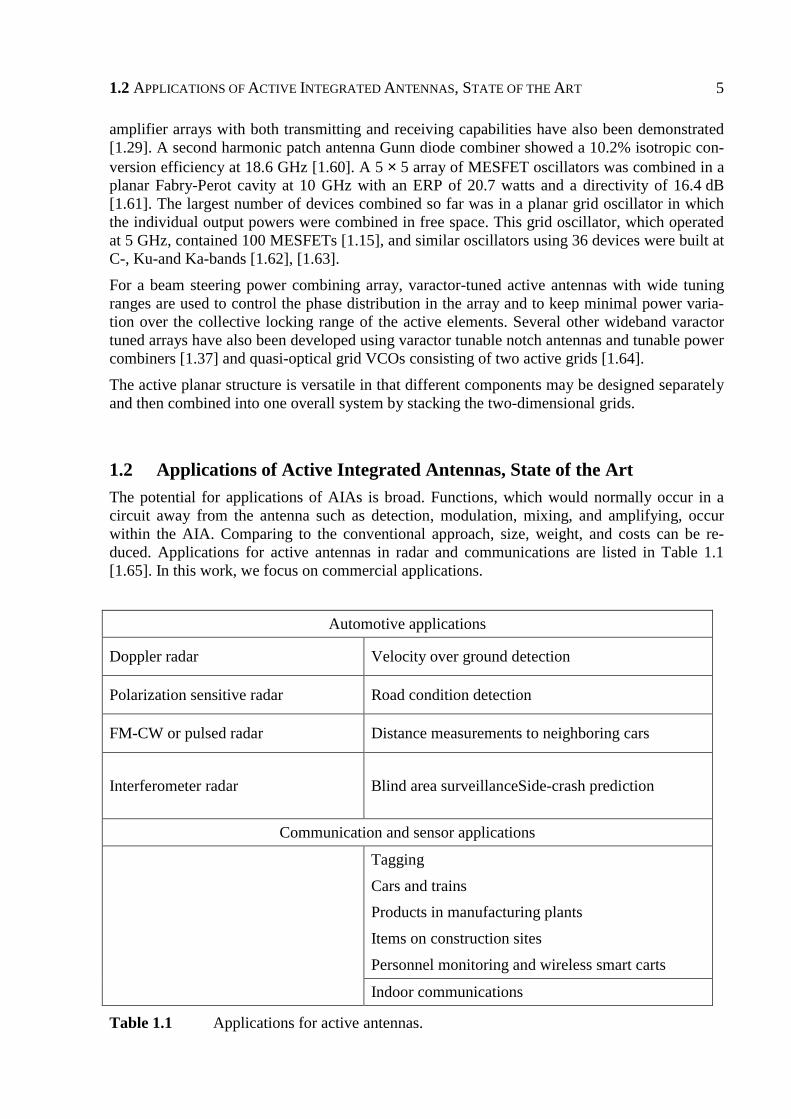
1.2 Applications of Active Integrated Antennas, State of the Art The potential for applications of AIAs is broad. Functions, which would normally occur in a circuit away from the antenna such as detection, modulation, mixing, and amplifying, occur within the AIA. Comparing to the conventional approach, size, weight, and costs can be re-duced. Applications for active antennas in radar and communications are listed in Table 1.1 [1.65]. In this work, we focus on commercial applications.
Automotive applications
Doppler radar Velocity over ground detection
Polarization sensitive radar Road condition detection
FM-CW or pulsed radar Distance measurements to neighboring cars
Interferometer radar Blind area surveillanceSide-crash prediction
Communication and sensor applications
Tagging
Cars and trains Products in manufacturing plants
Items on construction sites
Personnel monitoring and wireless smart carts
Indoor communications
Table 1.1 Applications for active antennas.

6 1 INTRODUCTION
Active integrated antenna arrays can also be used for the applications described in Table 1.1. Usage of arrays results in higher directivity and lower phase noise.
Civil applications require designated frequency bands accessible to everyone. For this purpose, ISM (Industrial, medical, and scientific) bands are defined. Most sensor applications use the bands at 433 MHz, 2.4 GHz, 5.8 GHz, and 24 GHz. Automotive applications can be found in the 24 GHz, 60 GHz, and the 76 GHz radar bands [1.66].
1.2.1 Automotive Applications Active antennas are inherently good Doppler sensors because radiating sources are sensitive to Doppler return from moving objects. The AIA serves as a mixer to mix the local oscillation frequency with the small frequency shift in the reflected wave from the moving object. Extract-ing this Doppler frequency shift allows relative motion to be detected. In comparison to a con-ventional radar system, AIA based Doppler radar is smaller, lighter, and cheaper. Multiple Doppler sensors have already been published [1.67], [1.68]. Two of them are based on AIAs [1.13], [1.19].
Schottky detectors can be integrated with the antenna for RF detection [1.69]. This detector can be used for many different monitoring or imaging applications (e.g. direction detection, [1.70]).
To measure the distance between a car and the borderline or other cars on the street, conven-tional automotive FM-CW sensors can be used [1.71], [1.72], [1.73].
FM-CW and Doppler sensors can be combined to a multifunctional sensor that is able to meas-ure the distance and velocity but also the tilt angle, height with respect to ground, and the direc-tion of motion. Using in addition polarimetric information enables the classification of road conditions [1.74].
The Doppler effect can be used not only for velocity measurements, but also for crash predic-tion and detection. The first crash sensor was published in 1972 [1.75]. Together with an AIA, the idea is revived in this work [1.76].
1.2.2 Sensor Applications (Non-Automotive) A common task in industrial applications is the online determination of the moisture content of bulk materials. This is usually done either by infrared or microwave absorption. These systems show the advantage that they measure the moisture remotely, under dirt conditions, and fast changing moisture contents (e.g. paper factory). The microwave transmission through a mate-rial can be measured using an AIA as the transmitter and a Schottky detector [1.77].
The Doppler frequency shift caused by moving objects can also be used for indoor intrusion alarm applications [1.78]. Due to their small size, AIAs can be hidden nearly everywhere to monitor e.g. strongrooms.
1.2.3 Communication/Tagging Applications The need for automatic identification of articles and personnel has grown rapidly in recent years with the increased use of computerized systems for security and control tasks. The primary limitation of traditional magnetically encoded cards is the need for physical contact between the card and the reader. Noncontact identifications systems in which identification can be made at a distance are either optical (bar code reader) or use radio frequencies. Radio frequency identifi-cation (RFID) systems have several advantages compared to optical systems, such as better penetration of obstructing materials (e.g. clothing, plastic cover) and easier processing of the

1.2 APPLICATIONS OF ACTIVE INTEGRATED ANTENNAS, STATE OF THE ART 7
identifying signals. In addition, RFID systems can be used for high-speed data transfers and synchronous read-write operation. Applications for RFID systems can be found in many areas:
• Personal badges for restricted area access, “Wireless Key”
• Anti-theft badges
• Luggage identification badges
• Automatic tolling Different types of RFID systems have already been realized. The most crucial part of the sys-tem is the mobile “tag” since it represents a stand-alone system that must be small, reliable, with a long lifetime, and further on it should be identified from a large distance. Depending on the read-range and lifetime, RFID tags can be divided into three types:
1. Remotely powered passive tags
2. Tags with battery powered signal processing
3. Active transmitting tags
Tags with no active RF front end get their RF energy from the interrogator. If they are interro-gated (“waked-up”) by a microwave beam, they emit a coded response [1.79]. Various types of response signals are in use, including simple backscatter with modulation in amplitude, phase, frequency, or combinations, or with a controlled time delay. Remotely powered fully passive tags (type 1) have to be operated in the near field region of the reader antenna. Though the read range can be enlarged using active signal processing (type 2), transmission distances are still very small [1.80], [1.81].
Tags with active RF front-end (type 3) can either be back-scattering [1.82], [1.83], [1.84] or independent transmitting tags as used in this work [1.85]. Lifetime depends strongly upon how often they are interrogated or sending their signal. They are used where long read-ranges are required. Since the RF front-end consumes more energy, the decrease in battery lifetime must be weighted against the increase in the read-range. The read-ranges of different RFID systems are shown in Table 1.2.
2.45 GHz passive responder [1.80] 0.3 m
2.45 GHz IC card system [1.82] 0.5 m
8 GHz transponder with AIA [1.83] 2 m
12 GHz transponder using subharmonic interrogation [1.81] 6 m
24 GHz active RFID system [1.85] 5-15 m
Table 1.2 Read ranges of different RFID systems.
For localizing objects outdoors, the global positioning system (GPS) can be used. However, GPS signals do not penetrate most construction materials, so objects in buildings cannot be tracked. To solve this problem, a 3D-ID tag has already been proposed [1.86]. This system has the constraint that many distributed detectors connected to a central computer are necessary to track things or people. Another system finding people and things indoor with only one receiver is presented in this work (compare [1.85]).

8 1 INTRODUCTION
1.3 Overview Active integrated antennas are the central elements of this work. The design processes, charac-teristics, and applications are discussed. The objective of this work is to show advantages and disadvantages as well as possibilities and restrictions using these antennas. The structure of the work can be summarized:
• Theory and design: Chapter 2 and 3
• Validation and characterization: Chapter 4
• Applications: Chapter 5. This work starts with the discussion of the design process of a free running AIA at 24 GHz. Different oscillator theories are presented and their applicability to active antenna design is dis-cussed. Oscillators are nonlinear circuits, but existing nonlinear CAD tools are complex and require good nonlinear device models, which are hard to obtain. Therefore, this work examines the validity and accuracy of a more practical linearized oscillator design described in chapter 2.
The properties of a free running AIA can be influenced in multiple ways. We focus on the fea-tures that are important for communication and sensor applications.
The frequency of the AIA can be tuned in two different ways. One method is to use the transis-tor bias to influence the oscillation frequency, another way is to make the frequency determin-ing resonator electronically tunable. For this purpose, the resonator is combined with a varactor diode. Different coupling methods are theoretically derived, implemented, and discussed re-garding the frequency and output power behavior over the tuning range in chapter 2.4.
The applicability of AIAs depends on their phase noise. The phase noise restricts the bit rate in communication applications and the local resolution considering sensor applications. The phase noise can be treated theoretically in multiple ways. We consider only the case of relatively high phase noise from unsynchronized oscillators. The consequences for the phase noise theory are discussed in chapter 2.5. In addition to the single AIA, the phase noise behavior of multiple coupled AIAs is also treated.
When dealing with oscillators, phase noise can be influenced by the quality factor (Q-factor) of the resonator. If a low-Q resonator is used (e.g. microstrip resonator), the Q-factor of the reso-nator dominates the phase noise behavior. The different definitions of the Q-factor are pre-sented to give a good insight for design in chapter 2.6. Applying this knowledge, different reso-nator shapes are investigated and their effects on the Q-factor are treated theoretically and com-pared with measurements. By using the optimal resonator shape, the phase noise can be re-duced.
The phase noise of the AIA can be improved further by increasing the resonator Q-factor with a dielectric resonator. The theory of these resonators is presented in chapter 2.7 and their applica-bility to AIA design is discussed.
Another way to influence the phase noise behavior of the AIA is using injection locking. An external locking source can be used to synchronize the AIA. The theory behind this synchroni-zation is presented in chapter 2.8 leading to the quantification of the injection locking properties of AIAs. The locking source can be either a low-noise highly stabilized oscillator or another AIA of the same type. If multiple AIAs are arranged at distances around a wavelength, they tend to couple, i.e. they influence themselves. This behavior is called mutual coupling and is discussed in chapter 2.9. Rigorous theory is needed to understand this behavior especially for a large number of coupled AIAs. We adapt coupling theory for an array of four antennas.
1.3 OVERVIEW 9
The oscillator theory described in chapter 2 is the starting point for the AIA design, which is evaluated in chapter 3. To complete the design process, oscillator theory must be combined with adequate models for the active device as well as the passive (i.e. microstrip) structure.
Two different transistors as well as IMPATT and varactor diodes are used as semiconductor devices within the AIAs. Their operation principle as well as their modeling is described in chapter 3.1 and chapter 3.2. The advantages using a rigorous oscillator model can be wasted if an inadequate semiconductor device model is used.
To model the passive structure of the AIA, two techniques are commonly used. Either micro-strip circuits can be modeled with circuit models (chapter 3.3), or full wave analysis is applied (chapter 3.4). Both techniques are introduced and compared.
Whereas the AIAs are designed in the first place to fulfill oscillation condition, radiating prop-erties must also be taken into account. In chapter 3.6, antenna properties are presented and adapted for AIAs.
After designing different antenna types, the results are validated with measurements in chapter 4. All relevant oscillator and antenna properties are characterized. The depiction starts with the free running AIA (chapter 4.2) followed by the voltage controlled (chapter 4.3) and the injec-tion locked AIA (chapter 4.4). The last section, chapter 4.5, deals with the characterization of a complete AIA array consisting of four AIAs.
The sensor and communication applications form the last chapter 5 of this work. Though many applications can be realized with AIAs, two are cited exemplarily. Representing a novel com-munication application, the first imaging RFID system is developed as part of this work. The development process, the realization, and the application of this system are portrayed in chapter 5.1.
As typical sensor application, the idea of an interferometer based crash sensor is revived in this work. A small sensor designed for the operation within a car door is developed based on an AIA in chapter 5.2. Real crash tests are carried through to gain some experience about the sen-sor behavior and to develop a suitable decision criterion that can be used for the coordination of different passenger protection devices within a car.
Finally, the results from this work are summarized and discussed in chapter 6.

2 OSCILLATOR THEORY APPLIED TO ACTIVE INTEGRATED ANTENNAS
In contrast to front-ends represented by an oscillator-antenna approach, the AIA is treated as a single entity. The drawback of this approach is that AIAs are difficult to design and their prop-erties differ from front-ends that were designed to fulfill a special task (i.e. highly stabilized transmitters or high directivity antennas).
In oscillator design, the interaction between the active element (diode, transistor) and the pas-sive microstrip circuit must be modeled. Three approaches are used in this work to model the AIA (Figure 2.1):
• Linear transistor model combined with linear multiport oscillator theory
• Linear transistor model together with the linearized injection locking theory introduced by Kurokawa
• Nonlinear transistor model combined with nonlinear harmonic balance oscillator theory.
Full-wave analysis of the passivepart of the the AIA
Linear transistormodel
Nonlinear transistormodel
Multiportanalysis
Kurokawa'sinjection locking theory
Oscillation frequencyStability Oscillation frequency
Phase noiseStability
Single AIAVoltage controlled AIA
Single AIAInjection locked AIACoupled AIAs
Single AIA
Harmonic BalanceAnalysis
Oscillation frequencyOutput power
2.1 2.2 2.2
2.32.4
2.32.82.9
2.3
Figure 2.1 Outline of the chapter.
For all approaches, the microstrip circuit is represented by a model derived from full-wave analysis. The circuit is discussed in detail in chapter 3.
Linear theory used in this work is described by the multiport approach combined with a linear transistor model (section 2.1). It is applied for the single AIA to simulate oscillation frequency and stability.

2.1 LINEAR THEORY 11
The linear transistor model is also combined with Kurokawa’s injection locking theory (section 2.2). Though this is originally a nonlinear approach, it is described in the work how it is com-bined with a linear transistor model. The advantage using Kurokawa’s theory is that in addition to the frequency and stability, the phase noise of the AIA can be modeled. Especially regarding injection locking and coupling, this approach is very effective.
The third approach presented in this work combines a nonlinear large-signal model of a transis-tor with nonlinear harmonic balance analysis (section 2.2). With harmonic balance, the output power can also be modeled. Since the output port for an AIA is the air interface, power simula-tion must be treated carefully.
Based on the desired design goals, the different oscillator theories are applied in the following sections.
A fixed frequency free-running AIA is simulated both with linear and nonlinear theory and the results are compared to show the applicability of the different approaches (section 2.3). Besides the fixed frequency, voltage controlled AIAs are also presented (section 2.4).
This chapter also deals with the improvement of the AIA properties. For this purpose, the influ-ence of the resonator shape on the phase noise (section 2.5) and Q-factor (section 2.6) is inves-tigated. Synchronization with dielectric resonators (section 2.7), injection locking (section 2.8), and coupling (section 2.9) completes this chapter.
2.1 Linear Theory Oscillator design based on linear theory neglects all nonlinear effects in the active device. Only one bias point is used, and it is assumed that this condition remains constant over the complete oscillator cycle (small-signal operation). The parameters of the transistor together with the pa-rameters of the passive circuit are used to derive the small-signal oscillation condition.
2.1.1 Derivation of Linear Oscillation Condition For linear modeling, the transistor description can be derived very easily. Small-signal meas-urements are sufficient to derive an S, Y, or Z-parameter description of the device. The simplest way to understand the oscillation mechanism is to use the concept of negative resistance: Con-trary to a positive resistance, a negative resistance is considered as a source of electrical energy since the product RI2 gives negative dissipated power. A transistor with three terminals needs an appropriate impedance to be connected to one or more terminals to create a negative resis-tance. When a load ZL is connected to the negative resistance ZT, with |ZL| < |ZT|, RF current is generated at a frequency at which the imaginary parts of both impedances cancel each other. An example for such a design is given in [2.1].
This RF current causes the value of the negative resistance to cancel unless the oscillation con-dition of –ZT = ZL is satisfied. In terms of wave reflection coefficients, this condition is ex-pressed as
1T LS S⋅ = (2.1)
2 , 0,1, 2,T LS S n nπ∠ + ∠ = = (2.2)
where ST and SL are the one-port S-parameter representation of the transistor and the resonator as depicted in Figure 2.2.

12 2 OSCILLATOR THEORY APPLIED TO ACTIVE INTEGRATED ANTENNAS
ZL ZT
Transistorand
embeddingcircuit
Resonator
ST SL
Figure 2.2 Schematic of a one-port microwave oscillator consisting of the active device in a negative resistance configuration and a resonator, which serves to determine the oscillation frequency.
Eq. (2.1) describes the oscillator loop consisting of the active device and the resonator. Since the resonator is lossy, the closed-loop gain Eq. (2.1) implies that the amplitude of ST must be larger than unity. The angle requirement Eq. (2.2) means that propagation time around the loop must be an integral number of oscillation periods or the electrical path be an integral number of wavelengths.
In order to analyze the oscillator, a test device must be inserted into the oscillator loop. This can be done by an appropriate two-port network. This two-port acts like a signal source, load, and ideal circulator. It turns the closed-loop oscillator into an open-loop amplifier. The location where the oscillator loop is split up may have influence on the derived oscillation frequency; compare [2.2]. The best place for splitting up the oscillator must be found experimentally. For visualization purposes, the open-loop gain can be drawn in a polar plot as the frequency is swept. Steady state oscillation occurs when the magnitude of the open-loop gain equals unity and the phase crosses zero. After the initial startup of the oscillator, as the amplitude of oscilla-tion begins to grow, the nonlinear nature of the active device means that the amplitude will reach a saturated level. This implies that the loop gain decreases from its small-signal value, finally reaching unity at some particular power level and frequency. Thus, the best estimate obtainable from the small-signal results is the zero crossing point of the open-loop gain phase. An easy way to determine the open-loop gain of an oscillator is for example to use the “osctest” element supplied by [2.3] and [2.4]. Accuracy using this element can be improved if the posi-tion and the impedance are chosen carefully [2.5].
Another way to derive an oscillation condition from the S-parameters is to consider the oscilla-tor as a combination of an active multiport and a passive multiport (the embedding circuit) as shown in Figure 2.3. With the active device and the embedding circuit characterized by their scattering matrices S, we have for the active device [2.6]
TTT aSb ⋅= (2.3)
and for the embedding circuit
p p p= ⋅b S a (2.4)
where a and b are the incident and reflected wave vectors, respectively, as indicated in Figure 2.3. When the active device and the embedding network are connected together, oscillation conditions becomes

2.1 LINEAR THEORY 13
Tp ab = (2.5) and T p=b a (2.6)
From Eqs. (2.3) to (2.6) we can write 0)( =⋅−⋅ ppT aISS (2.7)
where I is the identity matrix. Since for steady state 0≠pa , it follows that
ISSM −⋅= pT (2.8)
is a singular matrix or det M = 0 (2.9) This represents the generalized large-signal oscillation condition for an n-port oscillator. In fact, the S-matrix of the transistor being defined at the small-signal level, the n-port small-signal oscillation condition can be represented by:
( ) 0det >−⋅ ISS pT (2.10)
and ( ) 0det =−⋅ ISS pTArg (2.11)
Active Device
EmbeddingNetwork
aT1
bT1
aTn
bTn
ap1
bp1
apn
bpn
[S ]T [S ]p
u1
un
Figure 2.3 Schematic for general multiport oscillator configuration.
The oscillations can start up as soon as the preceding relations are satisfied and continue to build up until the device nonlinearities cause a steady state to be reached.
2.1.2 Stability Analysis Using Linear Oscillator Theory Eqs. (2.1) and (2.2) are widely used to predict the instability of the examined oscillator. It could be shown that in some cases this criterion is not necessarily true [2.5]. However, it can be re-placed by a Nyquist plot analysis [2.7]: The circuit is unstable if the Nyquist loop (ST·SL) encir-cles the point 1 + j0 in clockwise direction. If the resonator has a high Q so that it varies in fre-quency much faster than the active part of the circuit, the criterion can be rephrased in a form particularly convenient for applications. The system is unstable if the contour SL(jω) encircles 1 / ST. Consequently, it is easy to change parameters of the active circuit, so that the encircle-ment occurs. The method of stability circles [2.8] follows immediately from this formulation.
The Nyquist criterion can also be applied for the generalized n-port approach. In this case, the system is unstable if the Nyquist loop crosses the positive real axis in clockwise direction (Figure 2.11).

14 2 OSCILLATOR THEORY APPLIED TO ACTIVE INTEGRATED ANTENNAS
2.2 Nonlinear Theory In order to analyze and design AIAs accurately, a large-signal, nonlinear analysis should be applied. In the case of a single AIA, nonlinear analysis will give accurate prediction of oscilla-tion frequency, radiated power, and spectral output. In this section, a general derivation of the harmonic balance (HB) method is presented. This is necessary to understand the nonlinear os-cillator analysis included as an option in commercial design software. Regarding injection locked AIAs or multiple AIA systems, the synthesis becomes more complicated and cannot be done using available CAD tools. Combining the nonlinear analysis with Kurokawa’s oscillator and injection locking theory [2.9] allows modeling of this complex behavior. Introducing some approximations, it is moreover possible to use this theory with a linear transistor model.
2.2.1 Nonlinear Oscillator Model Based on Kurokawa Kurokawa’s oscillator model [2.9] is based on the assumption that the impedance of the device is a function of the RF current amplitude, whereas the resonator impedance is a function of ω. The frequency dependence of the device and the amplitude dependence of the resonator imped-ances are neglected. This assumption is valid for narrow bandwidths only but gives a good ap-proximation for our purpose.
For Kurokawa’s method, it is necessary to separate the AIA into the gate resonator and the tran-sistor plus embedding circuitry. Though the complete circuitry influences the oscillation behav-ior, it is shown that the AIA can be modeled with sufficient accuracy using this simplification. This partitioning also finds application regarding the radiation behavior. Figure 2.4 shows the separated AIA.
Gate resonator
Embedding circuit
Gate Source Drain
1640 µm
230 µm
650 µm
380 µm
Figure 2.4 Separated AIA structure.
An AIA can now be described by a simple circuit model. The nonlinear transistor is represented by an instantaneous current voltage relationship in the time domain so the nonlinear part of the device admittance is frequency independent. Any linear reactive part of the transistor admit-tance can be considered part of the embedding circuit; compare [2.10]. This separation is in accordance with the generalized HB approach (Figure 2.6). The possibility of externally in-jected signals is included via the independent current source Iinj (Figure 2.5).

2.2 NONLINEAR THEORY 15
-G (|V|)d
Iinj LL GL CC
Externalinjection
Resonator: YL
+
-
V
Transistorand embedding
circuit: Yosc
Figure 2.5 Single resonant negative conductance oscillator model of the injection locked AIA.
Considering an AIA denoted i, we can write from Kirchhoff’s current law (KCL)
( ) ( ) ( )iitiiinj VYVI ,~~,, ωωω = , (2.12)
where
( ) ( ) ( )[ ]ωωω iLiiosciit YVYVY ,,, ,, += (2.13)
is the total admittance. The tilde denotes a frequency domain phasor quantity. The next critical assumption in the analysis is that each AIA is a single mode system, designed to produce nearly sinusoidal oscillations around a nominal center frequency ωi; this is the free-running or unper-turbed oscillation frequency of the i-th oscillator. The AIA fulfills the criterion with a resonator having a Q>10, and the embedded transistor having a narrowband gain around resonance. The time dependent output voltage can then be written (using complex notation) in the following useful forms:
( )[ ]
tj
tji
ttjii
r
i
ir
etetAetAtV
ω
θ
φω
)(V)()()(
'i
)(
=== +
(2.14)
where Ai and φi are dynamic amplitude and phase variables, Vi’ = Ai exp(jφi) is the output “phasor” voltage at port i, θi(t) = ωrt + φi(t) is the instantaneous phase, and ωr is a reference frequency that is presumably close in magnitude to the average ωi, but otherwise somewhat arbitrary.
Applying the inverse Fourier transformation and exploiting the slowly varying amplitude and phase assumptions, Eq. (2.12) can be transformed to a coupled set of differential equations:
( )
−+=dt
dAA
jdt
dAYAYtVtI i
i
iiritritiiinj
1,),()()( ,
,,φ
δωωδ
ω (2.15)
This result is equivalent to using “Kurokawa’s substitution” for the frequency in Eq. (2.12), and it can be solved for the amplitude and phase variations by separating real and imaginary parts to give
)(Re , iiiii AFA
dtdA φ= (2.16)

16 2 OSCILLATOR THEORY APPLIED TO ACTIVE INTEGRATED ANTENNAS
),(Im iiii AF
dtd φφ
= (2.17)
where
( )( )
( )( )ωδωδ
ωφ
jAY
AYVIAF
irt
iritiiinjii ,
,, ,, −
= (2.18)
Eqs. (2.16) and (2.17) can be concisely written in complex form using Eq. (2.14) as
'i
''
V )( iii VF
dtdV
= (2.19)
which is a standard form for nonlinear analysis.
The total admittance near resonance for the circuit in Figure 2.4 is
( ) ( ) ( )0,, 2, ωωω −++= iiLidiit jCGAGAY (2.20)
where LC/10 =ω is the resonant frequency. It is convenient to express the dynamic equa-tions at microwave frequencies in terms of easily measurable quantities like resonant frequency and Q-factor. For a parallel resonator, we get Q =ω0 C/GL. Assuming a free-running AIA (no injection source, Iinj = 0), we have
( ) ( ) ( )riL
iidii j
GAG
QAF ωωωφ −+
+−= 0
,
,0 12
, (2.21)
which gives the dynamic equations
( )
+−= 1
2 ,
,0
iL
iidi
i
GAG
AQdt
dA ω (2.22)
rdtd ωωφ −= 0 (2.23)
The phase equation (2.23) can be easily integrated to give φ(t) = (ω0-ωr)t+φ0, where φ0 is an arbitrary constant. Substituting into Eq. (2.14) shows that the free-running frequency is always the resonant frequency, irrespective of the choice of ωr. From the perspective of solving for the phase dynamics, the clear choice for ωr in this case is ωr = ω0, which eliminates any time de-pendence of φ. This approach, though trivial in the present case, proves especially useful later for injection locked AIAs or AIA arrays. The important point is that a unique result is always obtained for the actual time variation of the output signal, regardless of the choice of ωr. How-ever, certain choices of reference frequency can simplify the description of the oscillator phase.
A steady state solution for the free-running amplitude α is determined from Eq. (2.22) by set-ting dA/dt = 0, which gives the oscillation condition
( ) 0,, =+ iLid GG α (2.24)
Applying these equations, we have a powerful tool to model not only a single AIA but also the injection locking and array behavior of the AIA.

2.2 NONLINEAR THEORY 17
2.2.2 Theory of Harmonic Balance Nonlinear Analysis AIA designs represent a demanding aspect for circuit synthesis. This is due to the dual use of the antenna element both as the radiating element and as the oscillator resonant load. An analy-sis technique for this type of situation, which accounts for the full nonlinear behavior of the large-signal device, is based on optimal oscillator design [2.11] adapted to include the micro-strip patch antenna as the oscillator resonant load; compare [2.12]. The synthesis process uses optimization as the core for a harmonic balance procedure, which finds a set of complex termi-nal large-signal voltages and currents at the gate (base) and drain (emitter) of the HEMT (HBT) device. These terminal conditions are selected by the harmonic balance procedure such that the specified added power necessary from the device, Padd, at the desired frequency of oscillation for given device bias conditions is derived as
( ) ( ) ( ) ( ) ( ) * *12add gs gs ds dsP f V f I f V f I f= − ℜ + (2.25)
where Vgs, Igs and Vds, Ids are the port voltages and currents of the input (gate-source) and output (drain-source) ports of the transistor in common source configurations, respectively.
The use of harmonic balance technique for high frequency circuit analysis was originally de-tailed by Hicks and Kahn [2.13] and Fillicori and Naldi [2.14]. Peterson and co-workers applied this technique to the large-signal analysis of MESFET devices in 1984 [2.15]. This simulation method is based on the ability to represent a nonlinear system as consisting of a suitably inter-connected linear and nonlinear subsystem [2.16]. Figure 2.6 shows the general form of a system partitioned for harmonic balance. The nonlinear subnetwork consists of nonlinear circuit ele-ments from the device model (nonlinear controlled sources, diodes, voltage dependent capaci-tors, current dependent resistors, etc.), whereas the linear subnetwork incorporates the linear circuit elements of the device model (resistors, capacitors, inductors and linear controlled sources, etc.) as well as the package parasitics and the passive circuit.
LinearPart ofDeviceModel
Transistor Chip
Non-LinearSubnetwork
LinearSubnetwork
PackageEquivalentCircuit
PassiveCircuit
v1N
i1N
vnN
inN
Y( ), S( )ω ω
I1L
INL
Figure 2.6 General form of a system partitioned for harmonic balance analysis.
Linear and nonlinear subsystems comprising the complete system are analyzed independently. When a high frequency electronic system is considered, it is generally desirable to represent the linear subsystem elements in frequency domain, typically Y(ω)- or S(ω)-parameters, while the nonlinear subsystem components may be represented by the appropriate time domain functional relationship (i.e. voltage and current vectors v(t) and i(t)). The solution of the system is achieved by balancing the terminal currents of the linear and nonlinear subsystems, IL(ω) and iN(t), at their interface, fulfilling Kirchhoff’s current law at each of the interconnected ports in the spectral domain. Fourier and inverse Fourier transformations are used to convert time do-main data to frequency domain data, and vice versa. Kirchhoff’s current law solutions are
18 2 OSCILLATOR THEORY APPLIED TO ACTIVE INTEGRATED ANTENNAS
reached by employing an iterative optimization approach to determine the currents that satisfy current and voltage balance at interconnected ports.
A general time domain representation of the nonlinear subnetwork could be of the form
∂∂
∂∂=
tt
ttt vviifi ),(,),()( (2.26)
where the vector f is a nonlinear function of various currents, voltages, and their time deriva-tives. Higher order derivatives may also appear. We assume that the vector function f is known from the nonlinear modeling of the transistor.
The linear subnetwork, on the other hand, can easily be analyzed by a frequency domain circuit analysis program ([2.3], [2.4]) and characterized in terms of an admittance matrix as
( ) ( ) ( )ωωωω JVYI +=)( (2.27)
where V and I are the vectors of voltage and current phasors at the subnetwork ports, Y repre-sents its admittance matrix, and J is a vector of Norton equivalent current sources. Analysis of the overall nonlinear circuit (linear subnetwork plus nonlinear subnetwork) involves continuity of currents given by Eqs. (2.26) and (2.27) at the interface between linear and nonlinear sub-networks.
In principle, the solution of the nonlinear circuit problem can always be found by integrating the differential equations that describe the system. However, we are interested in the steady state response with periodic excitations and periodic responses with a limited number of sig-nificant harmonics. This is why we use the harmonic balance method.
The frequency domain analysis of the linear subnetwork is carried out at a frequency ω0 and its harmonics. The characterization in Eq. (2.27) can thus be generalized as
( ) ( ) ( ) ( )0000 kV ωωωω kJkYkI k += (2.28)
where k = 1, ..., N, with N being the number of significant harmonics considered. The nonlinear subnetwork is analyzed in the time domain, and the response obtained is in the form of Eq. (2.26). A Fourier expansion of the current yields
( ) ( ) ( )
= =
N
kk tjkkt
000 expRe ωωFi (2.29)
where the coefficients Fk are obtained by a Fast Fourier Transform (FFT) algorithm. The piece-wise harmonic balance technique involves a comparison of Eqs. (2.28) and (2.29) and yields to a system of equations
( ) ( ) ( ) ( ) Nkkkkk kkk ,,1,0,00000 ==−− ωωωω JVYF (2.30)
The solution of this system of equations leads to the response of the circuit in terms of voltage harmonics Vk. Numerically, the solution of Eq. (2.30) is obtained by minimizing the harmonic balance error defined as
( ) ( ) ( ) ( ) ( )2
1
20000
−−=∆ ωωωωε kkkk kkb JVYFV (2.31)
Circuit optimization techniques are used for solving Eq. (2.30) to obtain steady-state periodic solution of nonlinear circuits. If a transient response is also desired (as for modulation aspects
2.3 COMPARISON OF OSCILLATOR THEORIES FOR AIAS 19
in arrays), it becomes necessary to use time domain techniques. A presentation of harmonic balance techniques incorporating Kurokawa’s oscillation criterion can be found in section 2.2.1.
If the solution of the harmonic balance synthesis is known, the external embedding circuit needed to fulfill the oscillation condition can be directly derived as presented in [2.16]. A more general approach to determine the embedding network can be found in [2.17]. An embedding network can be synthesized in any of three series or three shunt configurations. The network elements can be derived from Y-parameters of the active device at gain compression. They can be estimated by reducing the magnitude of S21 until the desired value of gain is obtained (sec-tion 2.3).
The numerical solution of the HB equations is straightforward if simulation software is used and the circuit is not too complex. If the steady state solution depends not only on one system but also on external injected signals and multi-oscillator systems, it is helpful to include Kuro-kawa’s oscillation condition given in [2.18] and [2.9].
In the following section, a generalized derivation of nonlinear oscillator theory considering in-jected signals and multi-oscillator systems is presented, which is adapted in the following sec-tions 2.8 and 2.9 that deal with injection locking and arrays.
2.2.3 Implementation of Harmonic Balance Analysis in Commercial Software Within commercial design software [2.3], there are elements that are helpful for the application of the HB synthesis. The “oscport” element is used as the test interface and the simulation pa-rameters are specified in an “HB analysis” box. Before starting the simulation, the frequency derived from linear analysis must be selected as the start frequency. DC supplies are directly connected to the transistor and the separation from the RF is realized via the idealized “DC Feed” and “DC Block” elements. Both the “DC Feed” element and the current supply need a parallel resistance having the order of some Gohms to stabilize the simulation. The simulation stability also depends on the impedance of the “oscport” element. Experiments performed for this work showed that values between 11 and 320 Ω lead to optimal results. One of the main problems associated with AIA simulation is that the module has no connection at which to measure the output power. Using commercial software, it is very difficult to model the radiation ports associated with AIAs. Therefore, measurements are in terms of radiated power measured at some distance from the antenna.
In chapter 3, harmonic balance is combined with full-wave simulation of the microstrip struc-ture to address this issue.
2.3 Comparison of Oscillator Theories for AIAs
2.3.1 Application of Linear Oscillator Theory The linear oscillator theory is applied to the free running AIA design developed in this work. It consists of a hybrid uniplanar microstrip structure, using a HEMT t409 (chapter 3) flip-chip mounted on the substrate allowing easy, inexpensive, and reproducible fabrication of the com-plete circuit. The resulting microstrip design with relevant dimensions is shown in Figure 2.7. The transistor is operated in a self-biased configuration with a VDS = 2.5 V and a 10 kΩ resistor between the gate and the source. The resistor enables the device to self-bias for a 24 GHz oscil-lation and enables stable oscillation.

20 2 OSCILLATOR THEORY APPLIED TO ACTIVE INTEGRATED ANTENNAS
Gate Source Drain
1640 µm
230 µm
650 µm
380 µm
Bias lines
Resonator/Antenna
Transistor PadsE
Figure 2.7 Layout of the 24-GHz AIA. The gate resonator is the radiating element. The radiated electric field is polarized as indicated.
The operation of the AIA in Figure 2.7 can be briefly described as follows: The main radiating part of the AIA is the nearly half wavelength long microstrip resonator connected to the gate of the transistor determining the polarization of the radiated (and received) wave. The drain of the transistor is terminated with a short non-resonant stub, and the short source stubs allow for a feedback loop by coupling to the gate resonator. The RF is decoupled from the bias lines by radial stubs.
Smal
l sig
nal o
scilla
tion
cond
ition
24 GHz
4 GHz
30 GHz
Imdet( * - )S S IT p
Redet( * - )S S IT p
Figure 2.8 Polar plot of Eqs. (2.10) and (2.11) as the frequency varies from 4 to 30 GHz.
Implementing linear (small-signal) oscillator theory, Eqs. (2.10) and (2.11) can be plotted in a polar diagram (Figure 2.8). The oscillation condition is satisfied if the curve crosses the positive real x-axis. This is satisfied in Figure 2.8 for the desired oscillation frequency of 24 GHz. Re-garding stability, the loop crosses the positive real axis in the clockwise direction, i.e. the sys-tem is unstable as desired.
2.3.2 Derivation of the Steady-State The optimal way to design oscillator is to use nonlinear (large-signal) oscillator theory. Since large-signal oscillator design is a difficult procedure requiring extensive large-signal measure-ments to obtain an adequate device model, it is interesting to verify if linear modeling gives sufficient accuracy for oscillator design. Many years ago, Vehovec, Houselander, and Spence [2.19] discussed an oscillator design method based on known device Y-parameters with the

2.3 COMPARISON OF OSCILLATOR THEORIES FOR AIAS 21
assumption that the voltages are nearly sinusoidal. This requires that the nonlinearities of the transistor are of a small degree. Later, Kotzebue [2.17] extended the work of Vehovec and de-rived a set of closed form solutions for the embedding elements of three series-type and three shunt-type oscillators based on small-signal S-parameter measurements. Using small-signal S-parameters, Maeda et al. [2.1] obtained meaningful oscillator design data at least for the oscilla-tion frequency. Besser [2.20] also acquired noteworthy design information based on small-signal measurements.
Regarding the two-port S(2)-parameters of a transistor with respect to different power levels, Johnson [2.21] showed that only |S21| changes under large-signal conditions. This means that the gain is saturating, while the other parameters are remaining constant when the oscillator reaches steady state. Therefore, it is sufficient to reduce |S(2)
21| to consider the saturation effects of the steady state.
To prove Johnson’s assumption with the transistor applied in this work, we measured the HEMT used for the AIA design with respect to different power levels. The power levels indi-cated in Table 2.1 are those of the VNA. In Table 2.1 it can be seen that Z21 depends much more on the power than the other parameters. This confirms that Johnson’s assumption can be applied in this work.
power Z11 Z12 Z21 Z22
-10 dBm 12.8-j22.7 64.9+j0 -8+j76.8 24.4-j36.3
-5 dBm 12.8-j22.7 64.9+j0.1 -8+j77.2 24.4-j36.4
0 dBm 12.8-j22.9 64.9+j0.1 -7.4+j76.8 24.4-j36.4
5 dBm 12.8-j22.9 64.9+j0.2 -6.4+j77.1 24.4-j36.5
10 dBm 12.8-j22.9 65.0+j0 -5.4+j77 24.4-j36.7
Table 2.1 Measured transistor parameters with respect to different power levels.
2.3.3 Linear Oscillator Design Using Reduced S-Parameters The conditions for a stable oscillation are given in Eqs. (2.5) and (2.6). Saturation effects al-ready took place and the transistor S(2)-parameters are at their steady-state (large-signal) values. Not considering transient effects, Eqs. (2.10) and (2.11) can be written as
( ) 0det =−⋅ ISS pT (2.32)
and ( ) 0det =−⋅ ISS pTArg (2.33)
Comparing the three-port oscillation conditions Eqs. (2.10) and (2.11) with Eqs. (2.32) and (2.33), it can be seen that the magnitude must be reduced whereas the argument remains un-changed. Looking at the reduced S(2)-parameters, we know from [2.21] that we only have to consider the variation of S(2)
21. Reducing S(2)21 by a factor of 0.44, the three-port steady state
oscillation condition (Eqs. (2.32) and (2.33)) is satisfied again.
22 2 OSCILLATOR THEORY APPLIED TO ACTIVE INTEGRATED ANTENNAS
Smal
l sig
nal o
scilla
tion
cond
ition
24 GHz
4 GHz
30 GHz
Imdet( * - )S S IT p
Redet( * - )S S IT p
Figure 2.9 Small-signal oscillation conditions to start oscillation (gray) and for stable os-cillation (black) as the frequency varies from 4 to 30 GHz.
In Figure 2.9, the oscillation conditions required to start up an oscillation and for steady state are plotted. Though the change of S21 is very large compared to the variation observed during the large-signal measurements according to [2.21], the divergence of the oscillation frequency using the reduced S-parameters is less than 1%. From this calculation, we know that the small-signal S-parameters can be used to predict oscillation frequency. Moreover, the steady state oscillation condition can easily be derived using Johnson’s [2.21] assumption that is proved valid for the transistor used in this work. To verify the validity of the reduced S-parameters they are applied to Kurokawa’s nonlinear oscillator theory.
2.3.4 Kurokawa’s Oscillation Condition with Reduced S-Parameters The free running AIA can also be examined using Eq. (2.24). After splitting up the AIA accord-ing to Figure 2.4, the admittances can be calculated. The S-parameters of the embedding circuit are combined with the reduced S-parameters of the transistor since Kurokawa’s theory is only defined for the steady state.
10 GHz 30 GHzFrequency
G+G d
L-0
.01
S0.
05 S
24 GHz
Figure 2.10 Kurokawa’s oscillation condition applied for a single AIA.
The result applying the reduced S-parameters to Kurokawa’s oscillator theory is shown in Figure 2.10. Oscillation condition is satisfied for 24 GHz. This confirms the validity of the re-duced S-parameters.
To examine this oscillation further, the Nyquist criteria (section 2.1.2) can be applied to the divided AIA structure. Figure 2.11 shows the Nyquist loop applied for Kurokawa’s oscillation condition. The loop encircles the point 1+j0 in clockwise direction, i.e. the AIA oscillates.

2.3 COMPARISON OF OSCILLATOR THEORIES FOR AIAS 23
Re * Γ ΓL d
Im * Γ ΓL d
1
2
4 GHz30 GHz
Figure 2.11 Nyquist criteria applied to Kurokawa’s oscillation condition as the frequency varies from 4 to 30 GHz.
2.3.5 Numerical Solution of the Oscillation Condition Using the reduced S-parameters, the oscillation condition, Eq. (2.9), is no longer an inequality and can be solved numerically.
Inserting Eq. (2.8) into Eq. (2.7) leads to
0)det( =−⋅ ISS pT (2.34)
ST and Sp are the three-port representations of the reduced small-signal S-parameters of the transistor and the S-parameters of the microstrip structure, respectively. The transistor and cir-cuit parameters can be derived from chapter 3.
It can be seen that Eq. (2.34) is the characteristic equation of ST·Sp for the eigenvalue 1. The corresponding eigenvector is ap in Eq. (2.7). The other wave vectors can be determined using Eqs. (2.3), (2.4), and (2.5), and the port voltages of the microstrip structure according to Figure 2.3 can be calculated:
( )pp bagU +⋅= 2 (2.35)
where
Ig ⋅= 0Z (2.36)
and the characteristic impedance is Z0. The port voltages are useful to calculate the radiated power and the far field distribution (chapter 3). Using the transistor S-parameters and the mi-crostrip data from the full-wave simulation and solving Eqs. (2.34) and (2.35), gives the follow-ing port voltages (Table 2.2):
Port Port voltage (magnitude) Port voltage (phase)
1 and 2 (source lines) 13.2 95°
3 (gate line) 15.18 -6°
4 (drain line) 4.94 -152°
Table 2.2 Calculated port voltages for the AIA configuration in Figure 2.3.

24 2 OSCILLATOR THEORY APPLIED TO ACTIVE INTEGRATED ANTENNAS
2.4 Frequency Tunable Active Integrated Antennas For some applications, it is required to use frequency tunable AIAs. An overview over these applications together with already proposed solutions is given in chapter 1. Tuning of AIAs can be achieved in two ways:
• Bias tuning of the active device. This has the advantage that the circuit topology of the fixed frequency approach can be used whereas the tuning range is very small.
• An additional varactor diode can be integrated into the circuit topology. This approach has a much wider tuning range but requires a redesign of the circuit and additional bias and control lines.
In this section the design process of a voltage controlled AIA with a varactor diode is described.
2.4.1 Background of VCOs Voltage controlled AIAs (VCAIAs) can be designed with linear oscillator theory (section 2.1) using a small-signal fixed frequency approach. Here, the circuit is divided into three parts con-sisting of the transistor, the diode, and the microstrip circuit (Figure 2.12). The transistor and the diode are modeled with its small- and large-signal representations, respectively. The deriva-tion of the models is described in chapter 3. The microstrip structure is simulated using a planar solver [2.22] based on the Method of Moments. The connections between the devices and the microstrip lines are modeled with point-feed ports simulating the physical flip-chip connec-tions. Geometric dimensions of the devices and bias lines together with RF decoupling circuits are taken into consideration during simulation.
TransistorModel
PassiveCircuitModel
DiodeModel
a b c
Figure 2.12 Modeling topology for the VCAIA.
Considering the transistor as the core element of the AIA, varactor diodes can be connected to any of the terminals of this device depending on their function. Varactors coupled to the gate are presented in [2.23], [2.24], [2.25], drain coupling is presented in [2.26], [2.27], and source coupling is shown in [2.28]. Coupling bandwidth can be further enlarged using two diodes at two different transistor terminals, e.g., gate and drain as shown in [2.29]. This symmetrical ap-proach is very useful if applied to arrays [2.30].
Varactor diodes are normally used in a shunted configuration. This is why many authors mount the diode through the substrate to allow a wideband ground connection. Since our fixed fre-quency approach is uniplanar, it was desired to mount the diode without a via-hole. Simulations showed that a RF ground connection with a radial stub is sufficient.
2.4.2 Frequency Tunable AIA Design In the AIA showed in Figure 2.7, the gate resonator is the frequency-determining element. Therefore, only the configuration where the diode is connected to the gate resonator is exam-ined. The influence of the diode on the oscillation frequency is examined as the diode voltage was varied for a diode model developed and integrated into the design (chapter 3). The oscilla-
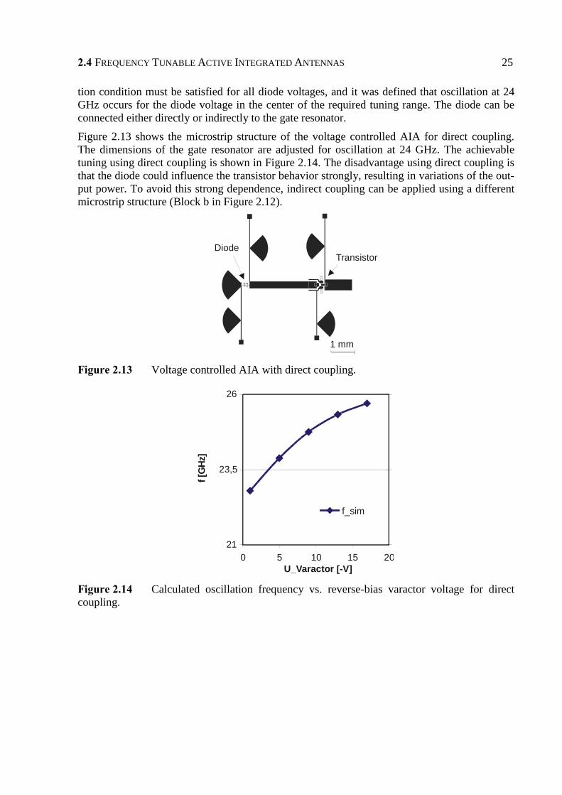
2.4 FREQUENCY TUNABLE ACTIVE INTEGRATED ANTENNAS 25
tion condition must be satisfied for all diode voltages, and it was defined that oscillation at 24 GHz occurs for the diode voltage in the center of the required tuning range. The diode can be connected either directly or indirectly to the gate resonator.
Figure 2.13 shows the microstrip structure of the voltage controlled AIA for direct coupling. The dimensions of the gate resonator are adjusted for oscillation at 24 GHz. The achievable tuning using direct coupling is shown in Figure 2.14. The disadvantage using direct coupling is that the diode could influence the transistor behavior strongly, resulting in variations of the out-put power. To avoid this strong dependence, indirect coupling can be applied using a different microstrip structure (Block b in Figure 2.12).
1 mm
DiodeTransistor
Figure 2.13 Voltage controlled AIA with direct coupling.
21
23,5
26
0 5 10 15 20U_Varactor [-V]
f[G
Hz]
f_sim
Figure 2.14 Calculated oscillation frequency vs. reverse-bias varactor voltage for direct coupling.

26 2 OSCILLATOR THEORY APPLIED TO ACTIVE INTEGRATED ANTENNAS
1 mm
1 mmDiode DiodeTransistor Transistor
a: inductive b: capacitive
Figure 2.15 Inductively (a) and capacitively (b) coupled voltage-controlled AIAs.
Capacitive and inductive coupling are studied in this work. Inductive coupling (Figure 2.15a) is realized with a thin (high impedance) line between the gate resonator and the diode, whereas the capacitive coupling (Figure 2.15b) is carried out with a coupled line section between the resonator and the diode. The capacitive approach includes an additional bias line for the diode. This line gives an additional degree of freedom as the diode is completely independently bi-ased, at the expense of real-estate increase. However, calculating time increases due to the addi-tional structures.
From Figure 2.16, it can be seen that the oscillation frequency is proportional to the diode volt-age for inductive coupling (a) but not for capacitive coupling (b). In Figure 2.16b, the oscilla-tion frequency increases for varactor voltages between [0; -8 V] and [-12 V; -18 V]. Between [-8V; -12 V], the frequency and radiated power decrease significantly. This indicates that multi-moding is occurring due to the modified resonator geometry.
23
24
25
0 5 10 15 20
U_Varactor [-V]
f[G
Hz]
f_sim
23
23,6
24,2
0 5 10 15 20
U_Varactor [-V]
f[G
Hz]
f_sim
a: inductive b:capacitive
Figure 2.16 Calculated oscillation condition for inductive (a) and capacitive (b) coupling.
The presented results clearly show that the configuration in Figure 2.15a is better regarding tuning range, overall size, and number of bias lines.
2.5 Phase Noise Many sensor and communication applications find their limitations in the phase noise behavior of the AIA. In this section, the phase noise is defined, and the physical mechanisms are dis-cussed. Besides free running AIAs, injection locked and AIA arrays are also considered. The

2.5 PHASE NOISE 27
noise free AIA model derived in the preceding sections is adapted. The influence of AIA pa-rameters, injection locking, and mutual coupling on the phase noise behavior is examined.
2.5.1 Definitions In frequency domain, the ideal oscillator signal is a discrete spectral line. However, due to dif-ferent noise mechanisms, there are phase and amplitude modulations that lead to a broader spectrum. There are two ways to describe this behavior.
Due to the random nature of the instabilities, the phase deviation is represented by a spectral density distribution plot. To measure phase instabilities, the spectral density of phase fluctua-tions on a per-Hertz basis Sφ(f) is used
( ) ( )ffS rms2φφ ∆= (2.37)
Frequency instabilities are described using the spectral density of frequency fluctuations as given in [2.31]
( ) ( ) ( ) ( )fSffffffS rmsrmsf φφ 2222 =∆=∆=∆ (2.38)
The spectral density of phase noise can be converted to the spectral density of frequency noise by multiplication with the Fourier frequency (corresponding to differentiation in the time do-main).
To measure the noise energy related to the RF power spectrum observed on a spectrum analyzer indirectly, L(f) can be used. L(f) is defined as the ratio of the power in one phase modulation sideband on a per-Hertz basis, to the total signal power. The phase noise density to carrier ra-tion L(f) is usually presented logarithmically as a plot of phase modulation sidebands in the frequency domain, expressed in dB relative to the carrier per Hertz of bandwidth [dBc/Hz]
=HzdBc
PowerCarriersidebandmodulationphaseOneDensityPowerfL )()( (2.39)
L(f) can be derived from Sφ(f)
( ) ( ) ( )fSf
fSfL f∆== 2
121
21
φ (2.40)
In the time domain, phase noise can be observed as phase jitter on an oscilloscope display, or a time interval counter may detect the instantaneous time fluctuations of the zero crossings. How-ever, this is difficult at microwave frequencies. Phase or frequency fluctuations are the same physical phenomena related by a time derivative. If v(t) is a signal with random phase fluctua-tion ∆φ(t), it can be written as [2.32]
( ) ( )[ ]ttfvtv s φπ ∆+= 02cos (2.41)
Frequency and phase are related in the time domain by
( ) ( )12
d tf tdtφ
π= (2.42)
In an oscillator, the signal consists of a large, relatively clean carrier accompanied by various forms of noise. The noise may initially be divided into two classes, noise at frequencies of the same order as the carrier and noise at relatively low frequencies, close to DC. Due to flicker effects in the active device used, noise close to DC tends to follow a 1/f power law with fre-quency. Since the active device is operated under large-signal conditions, the low frequency
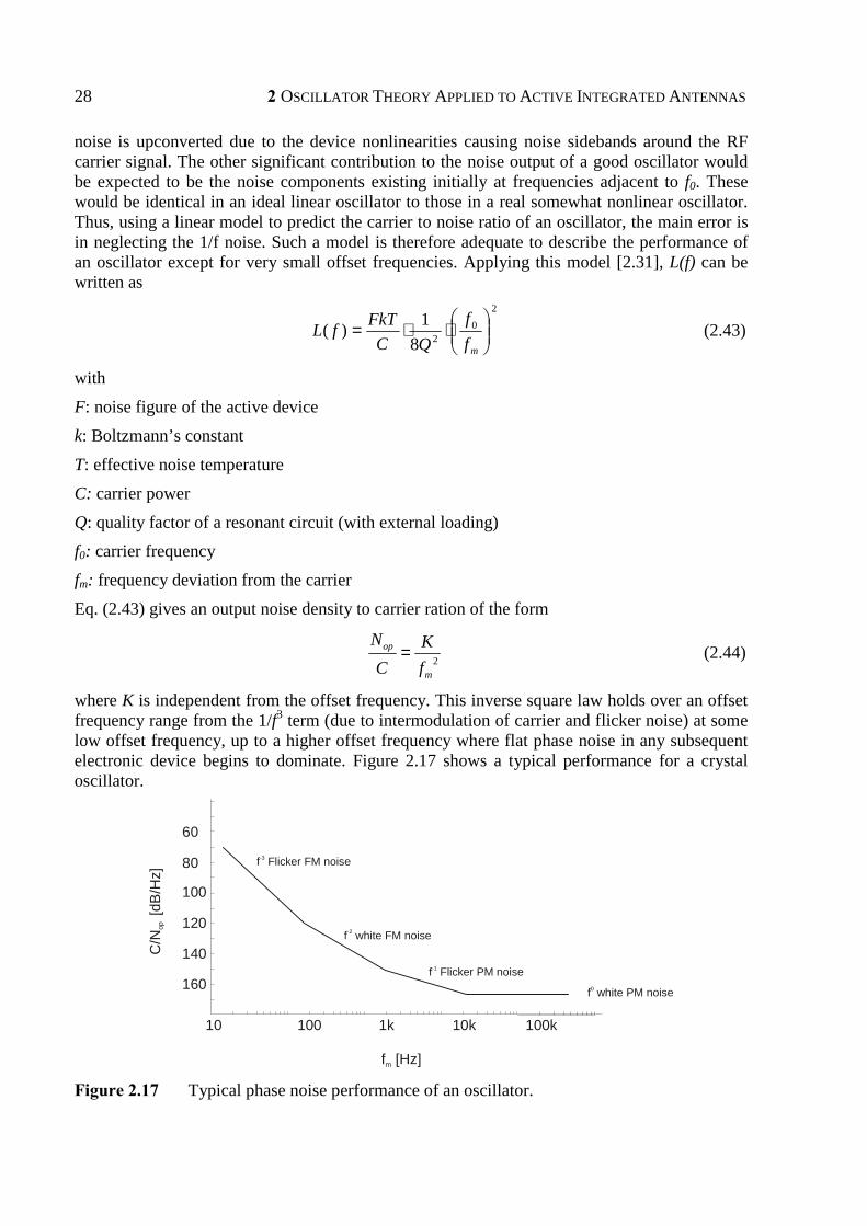
28 2 OSCILLATOR THEORY APPLIED TO ACTIVE INTEGRATED ANTENNAS
noise is upconverted due to the device nonlinearities causing noise sidebands around the RF carrier signal. The other significant contribution to the noise output of a good oscillator would be expected to be the noise components existing initially at frequencies adjacent to f0. These would be identical in an ideal linear oscillator to those in a real somewhat nonlinear oscillator. Thus, using a linear model to predict the carrier to noise ratio of an oscillator, the main error is in neglecting the 1/f noise. Such a model is therefore adequate to describe the performance of an oscillator except for very small offset frequencies. Applying this model [2.31], L(f) can be written as
2
028
1)(
⋅⋅=
mff
QCFkTfL (2.43)
with
F: noise figure of the active device
k: Boltzmann’s constant
T: effective noise temperature
C: carrier power
Q: quality factor of a resonant circuit (with external loading)
f0: carrier frequency
fm: frequency deviation from the carrier
Eq. (2.43) gives an output noise density to carrier ration of the form
2op
m
N KC f
= (2.44)
where K is independent from the offset frequency. This inverse square law holds over an offset frequency range from the 1/f3 term (due to intermodulation of carrier and flicker noise) at some low offset frequency, up to a higher offset frequency where flat phase noise in any subsequent electronic device begins to dominate. Figure 2.17 shows a typical performance for a crystal oscillator.
10 100 1k 10k 100k
f [Hz]m
160
140
120
100
80
60
C/N
op [d
B/H
z]
f Flicker FM noise-3
f white FM noise -2
f Flicker PM noise-1
f white PM noise0
Figure 2.17 Typical phase noise performance of an oscillator.

2.5 PHASE NOISE 29
2.5.2 Phase Noise in AIAs Due to the low Q of the distributed resonator, the linear oscillator model is sufficient since small frequency deviations cannot be determined. Furthermore, other factors that could affect the phase noise (power supply noise, nonlinearities of the transistor...) can be neglected.
This phase noise analysis extends the analysis from sections 2.8 and 2.9. This is done by using a complex noise admittance, which conveniently models the complexities of typical noise effects in AIAs [2.33]. The resulting dynamic equations describe the amplitude and phase fluctuations of the AIA. In a general case, the equations describe the transformation from amplitude modu-lation (AM) and phase modulation (PM) noise - corresponding to the real and imaginary parts of the noise admittance, respectively, to the individual oscillator output fluctuations. These equations cannot be solved analytically. However, restricting attention to phase noise and ne-glecting AM-to-PM conversion terms in the analysis permits an analytical solution.
As described in sections 2.8 and 2.9, a single negative resistance AIA model can be used to simulate the AIA, especially when regarding injection locking or arrays. This model is capable of generating all of the observed synchronization phenomena. Since the gate resonator is nearly half wavelength long, a parallel model is employed, as shown in Figure 2.18.
-G (|V|)d
Iinj LL GL CC
Externalinjection Gate Resonator
of the AIA
+
-
V
Transistorand embedding
circuit
Yn
Noise Admittance
Figure 2.18 Parallel negative conductance AIA model with complex noise admittance.
Noisy AIAs can either be modeled through the addition of an equivalent noise current generator or with an equivalent noise admittance Ynoise = Gnoise+jBnoise (compare [2.34]), as shown in Figure 2.18. To model both injection-locked and free running AIAs, an injection source is added to the model. The free running case can be considered by setting the injection current to zero. If the AIA is under-injection-locked to an external source, the phase relationship between the AIA and the injection source can be described as (section 2.8)
( ) ( )0 00 sin
2 2inj nd B tdt Q Q
ω ρ ωφ ω φ ψ= − − − (2.45)
where φ, ψinj are the instantaneous phases of the AIA and the injection signal, respectively, and ω0 and Q are the free running frequency and Q-factor of the AIA, respectively. ρ = Ainj/A is the injection strength (i.e. the injection signal is normalized to the free-running amplitude of the AIA). Bn(t) is a time varying noise susceptance (or the quadarture phase component of the noise admittance), assumed to be an ergodic process. A noise-free synchronized steady state satisfies
( )lock
inj
dB
injinj ω
ωωρω
ωωψφ
∆−
=−
=− 0
3
0ˆˆsin (2.46)
30 2 OSCILLATOR THEORY APPLIED TO ACTIVE INTEGRATED ANTENNAS
where ωinj = dφ/dt is the injection frequency, ω3dB = ω0/2Q is half the 3 dB bandwidth of the AIAs tank circuit, ∆ωlock = ρω3dB is half the entire locking range, and the circumflex (^) denotes a steady state quantity. Assuming the noise is a small perturbation of the noise-free solution, the phases change to
δφφφ +→ ˆ (2.47)
and
injinjinj δψψψ +→ ˆ (2.48)
where δφ and δψinj describe the small phase fluctuations of the AIA and injected signal, and Eq. (2.45) becomes
( ) ( ) ( )3
1 ˆ ˆcos inj inj ndB
d B tdtδφ ρ φ ψ δφ δψ
ω= − − − − (2.49)
Applying FFT algorithms, the power spectra density of the AIA phase fluctuation (the phase noise) can be calculated. In the absence of an injected signal, the phase noise of a free running AIA can be written as:
( )23
222
0
2~
~~~
dB
nuncoupledi
B
ωωφδφδφδ == (2.50)
The tilde denotes a transformed or spectral variable and ω is the noise frequency measured rela-tive to the carrier. The phase noise of an injection locked AIA can be written as:
( )( )
( ) ( )( )
( ) ( )222 2 2 2
2 3 02 22 2 2 2 2 2
3 3
ˆ ˆcos1 1ˆ ˆˆ ˆ2 2 cos cos
inj injdB
dB inj dB inj
L fρ φ ψ δψω ω δφ
δφω ω ρ φ ψ ω ω ρ φ ψ
−= = +
+ − + −
(2.51)
The result of Eq. (2.51) is essentially the same as that derived by Kurokawa [2.35].
The essential features of Eq. (2.51) are
1) The near carrier noise is approximately that of the injected signal over most of the lock-ing range, but approaches that of a free-running AIA at the band edges ( )/ 2injφ ψ π− ≈ .
2) The noise far from the carrier is that of the free-running AIA.
In practice, spurious phase modulation is more important technically than spurious amplitude modulation. This is because the majority of high capacity communication systems use angle modulation. Using a free running AIA as a signal source, only low bit-rate communication sys-tems can be realized. Large-signals received with heterodyne detectors can cover smaller sig-nals with their noisy sidebands. Moreover, the accuracy of velocity and distance measurements depends on the amount of phase noise of the signal source.
The phase noise behavior of an AIA depends on the active device. The transistor is responsible for the close-to-carrier phase noise due to the upconversion of the low-frequency noise. Since we neglect upconversion effects and the phase noise is primarily determined by the low-Q reso-nator, the influence of the transistor on the phase noise is neglected. A comparison of the differ-ent transistor performances (HBT and HEMT) can be found in [2.36].

2.5 PHASE NOISE 31
There are different ways to improve the phase noise of AIAs. The phase noise of a free running AIA can be improved by increasing the Q of the microstrip resonator (see section 2.6). Addi-tionally, AIAs can be combined in self-locked arrays.
2.5.3 Phase Noise in Coupled AIAs Coupled-oscillator systems possess synchronization properties that may be suitable for certain millimeter wave power combining and beam scanning applications. To ease mutual locking, low-Q oscillators are preferred that unfortunately imply large phase noise. It can be shown that the total phase noise of an array can be reduced compared to a single free-running element in an array in direct proportion to the number of array elements used, if the coupling network is de-signed properly. Considering an AIA array, it is assumed that the independent noise sources of the oscillators are mutually uncorrelated but generate identical power spectra. As the coupling phase deviates from the optimum value, the phase noise can increase significantly near the locking range edge, depending on the offset frequency from the carrier.
The AIA array is modeled according to section 2.9. Each AIA is represented again as a parallel resonant circuit with complex noise admittance Yn (section 2.5.2) and coupling is modeled us-ing a coupling network that is described by Y-parameters. To model the influence of injection locking within the array, independent current sources are added to the model. The general case of a mutually coupled AIA array can be derived setting all current sources to zero. The resulting model is shown in Figure 2.19.
Iinj,1
Iinj,2
Iinj,N
Osc#1
Osc#2
Osc#N
Yosc,1
Yosc,2
Yosc,N
V1
V2
VN
YL,1
YL,2
YL,N
+
+
+
-
-
-
Cou
plin
g ne
twor
k
(Y p
aram
eter
s)
-G (|V|)d
L C
Yn
Figure 2.19 Oscillators coupled in parallel through an arbitrary network described by Y-parameters. A set of mutually coherent sources apply injected signals at each port.
The current sources are assumed to be mutually coherent at a frequency ωinj, but have arbitrary amplitude and phase. Adapting the methods derived in section 2.9, the phase dynamics of an N-element array are predominantly governed by [2.34]:
( ) ( ) ( )1
Im sin2
j iN
ji ii ij i i i ni
j
d e B tdt Q
φ φφ ωω κ ρ φ ψ−
=
= − + − + (2.52)
for i = 1,2,...N, where the following parameters have been used to describe the i-th oscillator:
ωi free-running frequency
φi instantaneous phase
ρi normalized injected signal amplitude

32 2 OSCILLATOR THEORY APPLIED TO ACTIVE INTEGRATED ANTENNAS
ψi instantaneous phase of the injected signal Bni noise susceptance
Q Q-factor of the AIA
We also assume that the oscillator amplitudes are approximately the same. The coupling pa-rameters κij are defined by
L
ijij G
Y=κ (2.53)
where Yij describe the admittance or Y-parameters of the coupling network, and GL is the load conductance required for the free-running AIA to achieve the desired amplitude.
The power spectral density of the phase fluctuations of the AIA array is derived according to the single AIA approach using perturbation of the noise-free solution. The following substitu-tions are made in Eq. (2.52):
δφφφ +→ ˆ (2.47)
and
injinjinj δψψψ +→ ˆ (2.48)
Assuming δφi and δψinj are small, and performing a Fourier transform gives for a globally in-jected array
( )
( ) ( )23
2
22
23
2
232
0
2
~
~1~
dBinj
dB
dBtotal N ωωρ
ρψδωωρ
ωωφδφδ+
++
= (2.54)
The term |δφ0|2 is the noise of a single free-running AIA, Eq. (2.50). The total noise has exactly the same form as the result obtained for a single injection locked AIA, except that the contribu-tion from internal noise sources in the array is reduced by 1/N. Near the carrier, the output phase noise is that of the injected signal
22
0
~~lim injtotal ψδφδω
=→
(2.55)
and far from the carrier, the noise reduces to that of a free running synchronized array as fol-lows
22 ~1~lim 0∞→
= φδφδω Ntotal (2.56)
In a mutually coupled AIA without external injection locking, the phase noise for all frequen-cies can be described as:
22 ~1~uncoupledtotal N 0= φδφδ (2.57)
The total phase noise for N mutually coupled AIAs becomes 1/N of that of a single AIA. This suggests that mutual synchronization does not lead to any significant correlation of the AIA phase fluctuations.
The noise property of the individual AIA in the mutual coupled array is also of interest. The power spectral density of the i-th AIA in the array is found as given in [2.37]:
2.6 Q-FACTOR 33
2
22
2
2 ~~uncoupledi
lock
locki
N
Nφδ
ωω
ωω
φδ
∆+
∆+
= (2.58)
Again, the primary interest is with the phase noise near the carrier, so that ω<<∆ωlock, in which case
22 ~1~uncoupledii N
φδφδ → (2.59)
At the other extreme (i.e. far from the carrier), the individual AIAs approach the free-running noise properties:
22 ~~uncoupledii φδφδ → (2.60)
To summarize, after adding the coupling circuits, the individual AIAs and the total array output have a phase noise reduction near the carrier frequency in direct proportion to the number N of AIAs. The phase noise of an AIA far from the carrier frequency is not affected by the coupling circuits and still has the same noise properties as the free running AIA.
2.6 Q-Factor In microwave integrated circuits, resonant systems can be realized in different ways depending on the waveguide technology used. In this work, microstrip technology is applied. Microstrip resonators can have either ring, circular, or rectangular shapes. Since we use the resonators also as radiators, ring or circular patch shapes are not applied due to their varying polarization. The only patch shape considered in this section is a rectangular patch/resonator.
Regarding the resonator/antenna of an active integrated antenna, there is a contradiction in the desired properties. On the one hand, a high-Q resonator is desired to allow for low-noise. On the other hand, a low-Q patch antenna with high radiation efficiency is welcome. A compro-mise between the oscillator/antenna functions must be found.
Within an AIA, the resonator is directly connected to the active device. This results in a second compromise that must be found for the input impedance of the resonator/antenna. Only these input impedances satisfying oscillation condition can be used. In this section, electric as well as geometric factors that influence the Q-factor of the AIA are discussed.
2.6.1 Definitions of Q-Factors
2.6.1.1 Unloaded Q-Factor
An important parameter specifying the frequency selectivity and performance of a resonant circuit in general, is the quality factor, Q-factor, or Q. A very general definition of Q that is applicable to all resonant systems is [2.38]
0 0peak energy stored in the resonatorQ
average power lost per cycle in the resonatorω= (2.61)

34 2 OSCILLATOR THEORY APPLIED TO ACTIVE INTEGRATED ANTENNAS
For a parallel resonant circuit it can be written as
ppp
p
CLGC
Q0
00
1ω
ω== (2.62)
2.6.1.2 Loaded and External Q-Factors
In practical situations, the resonant circuit is coupled to an external load GL (i.e. the source ad-mittance) that also dissipates power, and the loaded quality factor QL is given by
eL QQQ
111 += (2.63)
where Qe is the external Q for a lossless resonator in the presence of the load
0epeak energy stored in the resonatorQ
average power lost per cycle in the loadω= =
L
p
GC0ω
(2.64)
0Lpeak energy stored in the resonatorQ
average power lost per cycle in the resonator loadω=
+=
pL
p
GGC+
0ω (2.65)
2.6.2 Influence of Various Loss Contributions on the Q-Factor The main losses in a microstrip line are due to radiation and the finite conductivity of the metal. However, to keep the results as realistic as possible, dielectric losses, surface roughness, and dispersion are included in this examination, although their influence on the overall Q in many cases is relatively minor.
Here, only open-circuited transmission lines (OC-TL) are discussed. If the length of the resona-tor is about a half of a guided wavelength, it behaves close to resonance as a parallel resonant circuit.
Belohoubek and Denlinger [2.39] reported Q-factor calculations for λ/4 resonators (one side shortened) over a limited frequency range. Gopinath [2.40] presents a method to calculate the Q-factors of half-wavelength resonators as a function of conductor, dielectric, and radiation losses.
The overall Q of the resonator is given by:
rdct QQQQ
1111 ++= (2.66)
where Qc, Qd, and Qr are the Q-factors associated with conductor loss, dielectric loss, and radia-tion loss, respectively. From Eq. (2.66), it can be seen that the total Q is always dominated by Q-factor related with the highest losses.
The high current density in the edge regions of the thin conducting strip is a source of loss for microstrip lines at microwave frequencies. Pucel [2.41] derived curves for the conductor at-tenuation factor αc·Z0·h/Rs as a function of w/h and t/h. These curves can be used to determine the conductor loss constant αc. Ζ0 is the characteristic impedance of the microstrip line depend-ing on the line width w, h and t are the substrate and metallization thickness’, and Rs denotes the surface skin resistivity of the conductor:
2.6 Q-FACTOR 35
0
0
λρπ Z
Rs = (2.67)
where ρ is the resistivity of the metallization. After determining αc from the corrected curves in [2.41], the conductor Q-factor can be calculated:
gc
cQλα
π= (2.68)
Since dielectric loss is usually lower than conductor loss, a detailed estimate of dielectric losses is not necessary, and it can be described as:
[ ]mNpq
geff
rd λε
δεπα tan= (2.69)
where
11
−−
=r
effqεε
(2.70)
εeff effective dielectric constant εr substrate relative dielectric constant λg guided wavelength tan δ substrate loss tangent The dielectric Q-factor Qd can be calculated from the dielectric loss constant αd:
dg d
Q πλ α
= (2.71)
A theoretical paper by Lewin [2.42] discusses radiation from discontinuities in microstrip. One of the cases considered, an open circuit, is applicable to the transmission line resonator configu-ration [2.43]. Since the length of the resonator is small compared to the free-space wavelength, the radiation from the two ends is not independent and further adaptations must be made. Gopi-nath [2.40] presents a formula for the radiation quality factor for a λg/2 resonator, valid for resonators used in this work:
2
200
323
hZ
Q effr η
λε= (2.72)
where η is the free-space characteristic impedance and h is the substrate thickness. From Eq. (2.72), it can be seen that the Q-factor due to radiation losses is limited by low dielec-tric constant (εr) substrates as well as low impedance (Z0) lines.
Line impedance can be adapted changing the line width. Enlarging the radiating edge results in lower impedance and lower radiating Q Eq. (2.72), Figure 2.20. On alumina, a 25 Ω line radi-ates about 25% of the total dissipated power in a resonant circuit. A 10 Ω line would radiate 50%, and an impedance below 5 Ω would be impractical due to 100% radiation loss, compare [2.44]. However, line impedance cannot be increased too much since high impedance is corre-lated with excitation of surface waves resulting in increased losses.

36 2 OSCILLATOR THEORY APPLIED TO ACTIVE INTEGRATED ANTENNAS
0.05 mm
0.05 mm
0.05 mm
0.1 mm
0.1 mm
0.1 mm
0.2 mm0.2 mm
0.2 mm
0.375 mm
0.375 mm
0.375 mmQr
Q0
Qt
11
10
10
100
100
1000
1000
10000
Q-fa
ctor
Impedance
Figure 2.20 The Q-factor of λ/2 resonators against impedance for different substrate thick-ness’ (f = 32 GHz, ε r= 13 [2.40]).
For alumina substrates and low frequencies, the Q-factor is determined by the circuit losses, whereas the radiation losses are not very pronounced. At higher frequencies, however, and es-pecially for low characteristic impedance lines and thick substrates, radiation dominates. Figure 2.20 shows the total Q-factor of half wavelength resonators versus impedance (i.e. line width) for different substrate thickness. To simplify the graph and show the effect of radiation losses more clearly, the circuit quality factor Q0 = 1/Qc+1/Qd is used. The total Q, Qt is dominated for low impedance lines by the radiation losses (i.e. Qr), and for high impedance lines by conductor and dielectric losses (i.e. Q0), respectively.
At each impedance, the curve peaks to a maximum value of Q at some substrate thickness. This maximum Q decreases whereas the substrate thickness, at which the maximum Q occurs, in-creases with increasing impedance.
Though Figure 2.20 does not represent our exact boundary conditions (εr = 10, h = 0.254 µm, f = 24 GHz), it is a good approximation. Comparing the Q-factor behavior given in Figure 2.20 with the maximum Q-factor that can be achieved using our boundary conditions (Figure 2.21), it can be seen that the information in both graphs agrees with respect to the value of Qopt.
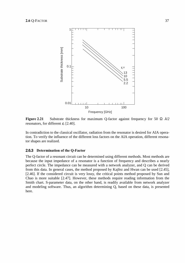
2.6 Q-FACTOR 37
10 1000.01
0.1
1
Subs
trate
thic
knes
s [m
m]
Frequency [GHz]
εr=13105.52.2
Figure 2.21 Substrate thickness for maximum Q-factor against frequency for 50 Ω λ/2 resonators, for different εr [2.40].
In contradiction to the classical oscillator, radiation from the resonator is desired for AIA opera-tion. To verify the influence of the different loss factors on the AIA operation, different resona-tor shapes are realized.
2.6.32.6.32.6.32.6.3 Determination of the Q-Factor The Q-factor of a resonant circuit can be determined using different methods. Most methods are because the input impedance of a resonator is a function of frequency and describes a nearly perfect circle. The impedance can be measured with a network analyzer, and Q can be derived from this data. In general cases, the method proposed by Kajfez and Hwan can be used [2.45], [2.46]. If the considered circuit is very lossy, the critical points method proposed by Sun and Chao is more suitable [2.47]. However, these methods require reading information from the Smith chart. S-parameter data, on the other hand, is readily available from network analyzer and modeling software. Thus, an algorithm determining Q, based on these data, is presented here.

38 2 OSCILLATOR THEORY APPLIED TO ACTIVE INTEGRATED ANTENNAS
-G (|V|)d
LLL GL CLC
Resonator
+
-
V
Transistorand embedding
circuit
YT YL
Figure 2.22 Definition of the admittances to derive the Q-factor of the AIA.
The representation of Q, to be used as the basis for the present method, begins with representing the circuit to be determined in terms of a parallel admittance YL (since the examined resonator is nearly half-wavelength long, see Figure 2.22) as expressed in [2.48]
LLL jBGY += (2.73)
with
( )
*
4VV
WWB HEL
−= (2.74)
where WE and WH are the stored electric and magnetic energies, respectively, in the system; and V is the input voltage. Furthermore, it can be shown that
*4
VVWWB HEL +=
δωδ (2.75)
where WE + WH is the average energy stored in the system. The average power lost in the sys-tem is given by
( )TL YGVVlostpowerAverage += *
21 (2.76)
Substituting Eqs. (2.75) and (2.76) into the fundamental definition of Q in Eq. (2.61) gives the following representation for the loaded QL:
( )0
2 ωωδωδω
=
+= B
YGQ
TLL (2.77)
With this expression, QL can be evaluated using either simulated or measured S- or Y-parameters. Since Y-parameters cannot be measured directly using a network analyzer, [2.48] can be used to convert S-to Y-parameters. Since these parameters are normally given in discrete form, a numerical derivative for δB/δω is required:
( ) ( )( )
( ) ( )22
n B BBn
ω ωδδω ω ω
−≅
−
(2.78)
where n is the number of discrete points of data used to calculate the slope.
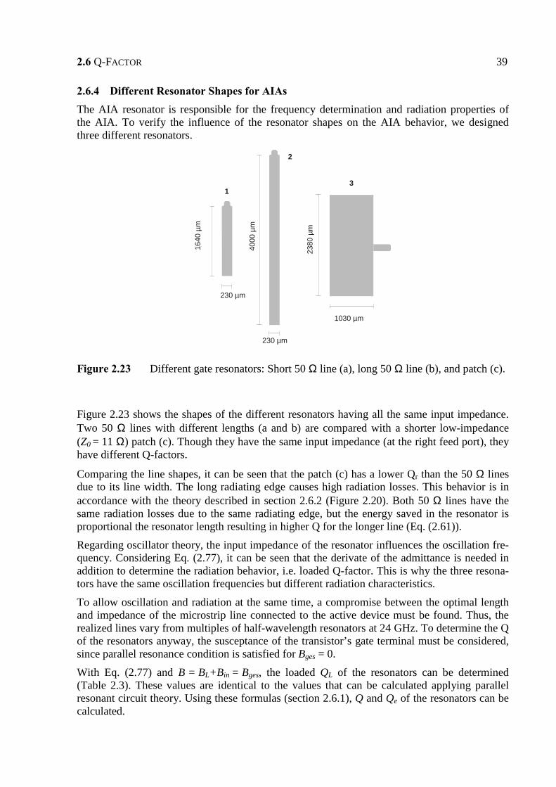
2.6 Q-FACTOR 39
2.6.4 Different Resonator Shapes for AIAs The AIA resonator is responsible for the frequency determination and radiation properties of the AIA. To verify the influence of the resonator shapes on the AIA behavior, we designed three different resonators.
1640
µm
230 µm
230 µm
4000
µm
1030 µm23
80 µ
m
1
2
3
Figure 2.23 Different gate resonators: Short 50 Ω line (a), long 50 Ω line (b), and patch (c).
Figure 2.23 shows the shapes of the different resonators having all the same input impedance. Two 50 Ω lines with different lengths (a and b) are compared with a shorter low-impedance (Z0 = 11 Ω) patch (c). Though they have the same input impedance (at the right feed port), they have different Q-factors.
Comparing the line shapes, it can be seen that the patch (c) has a lower Qr than the 50 Ω lines due to its line width. The long radiating edge causes high radiation losses. This behavior is in accordance with the theory described in section 2.6.2 (Figure 2.20). Both 50 Ω lines have the same radiation losses due to the same radiating edge, but the energy saved in the resonator is proportional the resonator length resulting in higher Q for the longer line (Eq. (2.61)).
Regarding oscillator theory, the input impedance of the resonator influences the oscillation fre-quency. Considering Eq. (2.77), it can be seen that the derivate of the admittance is needed in addition to determine the radiation behavior, i.e. loaded Q-factor. This is why the three resona-tors have the same oscillation frequencies but different radiation characteristics.
To allow oscillation and radiation at the same time, a compromise between the optimal length and impedance of the microstrip line connected to the active device must be found. Thus, the realized lines vary from multiples of half-wavelength resonators at 24 GHz. To determine the Q of the resonators anyway, the susceptance of the transistor’s gate terminal must be considered, since parallel resonance condition is satisfied for Bges = 0.
With Eq. (2.77) and B = BL+Bin = Bges, the loaded QL of the resonators can be determined (Table 2.3). These values are identical to the values that can be calculated applying parallel resonant circuit theory. Using these formulas (section 2.6.1), Q and Qe of the resonators can be calculated.

40 2 OSCILLATOR THEORY APPLIED TO ACTIVE INTEGRATED ANTENNAS
Line No. QL, Eq. (2.77) Qe, Eq. (2.64) Q0, Eq. (2.62)
a 9.17 9.86 130.4
b 17.6 20.6 120.8
c 7.0 7.45 115.8
Table 2.3 Calculated Q-factors for the different resonators from Figure 2.23.
Resonator (b) has indeed the highest Q0 (Table 2.3). Without the load of the transistor, the reso-nators behave nearly identical. This result is in agreement with Figure 2.20.
The Q-factors in Table 2.3 are derived from Y-parameters based on full-wave simulations with the Method of Moments. To verify these results, Q can also be determined based on the physi-cal loss mechanisms (section 2.6.2). If the frequency and substrate parameters are known, Eqs. (2.66) to (2.72) can be used to calculate the Q of the resonator based on physical effects. With the oscillation frequency set to 24 GHz and the substrate parameters from the appendix, Q can be determined to be 160. This value is 23% larger than the value derived from the simulated Y-parameters. This error is due to the assumption that the resonator is exactly half wavelength long, which is not true. However, the calculation based on the loss mechanisms proves the va-lidity to use the transistor susceptance for the calculations.
The resonator Q is not only influenced by the resonator shape, but also by a high-Q resonator coupled to the original line resonator. This case is considered in the following section.
2.7 Dielectric Stabilized Active Integrated Antennas Dielectric resonators (DRs) can be used as hybrid circuit elements in microstrip circuits. These resonators function as band pass and band stop filters or stabilization devices for oscillators. DRs are small cylinders and have a high Q due to high ε material (ε > 30), making them desir-able for microstrip circuits where the resonators have low-Qs.
For active antennas, several basic configurations are possible. The DR may be placed at either the output or input of the active device. However, using a DR broader tuning bandwidths are supposed to be obtained if the DR works as a parallel feedback element. In this section, it is verified how the DR can be integrated into the AIA leading to better antenna properties.
2.7.1 Dielectric Resonator Modes Besides the TE and TM modes, a hybrid, or HEM mode that can be either quasi-TE or quasi-TM exists in a dielectric resonator, see [2.8]. This mode occurs in the dielectric resonator be-cause a magnetic or tangential electric field normal to the resonator wall can exist. Neither of these is possible at a metal wall.
Analysis of a dielectric resonator is complex although much work has been done to obtain good design information [2.49]. Due to the cylindrical form of the rod, the solutions to Maxwell’s equations will be Bessel functions. For propagation, the Bessel function of the first order ap-plies inside the rod, since this is the only function that is finite at the rod’s center. Outside of the rod, the Bessel function of the second order (sometimes referred to as the Neumann function) applies because it vanishes as its argument increases without limit.
If the rod is cut into a short section, then again the field equations can be satisfied. A rather complicated eigenfunction results, showing conditions for resonance of the rod in free space.
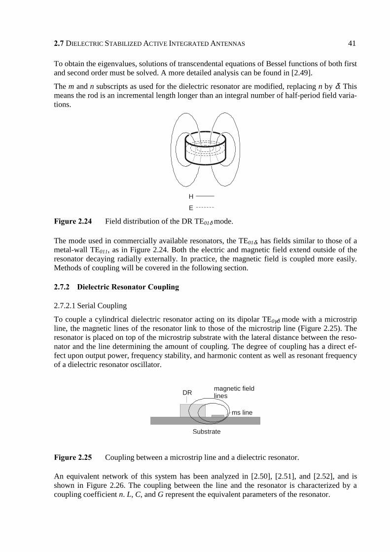
2.7 DIELECTRIC STABILIZED ACTIVE INTEGRATED ANTENNAS 41
To obtain the eigenvalues, solutions of transcendental equations of Bessel functions of both first and second order must be solved. A more detailed analysis can be found in [2.49].
The m and n subscripts as used for the dielectric resonator are modified, replacing n by δ. This means the rod is an incremental length longer than an integral number of half-period field varia-tions.
H
E
Figure 2.24 Field distribution of the DR TE01δ mode.
The mode used in commercially available resonators, the TE01δ, has fields similar to those of a metal-wall TE011, as in Figure 2.24. Both the electric and magnetic field extend outside of the resonator decaying radially externally. In practice, the magnetic field is coupled more easily. Methods of coupling will be covered in the following section.
2.7.2 Dielectric Resonator Coupling
2.7.2.1 Serial Coupling
To couple a cylindrical dielectric resonator acting on its dipolar TE0γδ mode with a microstrip line, the magnetic lines of the resonator link to those of the microstrip line (Figure 2.25). The resonator is placed on top of the microstrip substrate with the lateral distance between the reso-nator and the line determining the amount of coupling. The degree of coupling has a direct ef-fect upon output power, frequency stability, and harmonic content as well as resonant frequency of a dielectric resonator oscillator.
Substrate
DR magnetic fieldlines
ms line
Figure 2.25 Coupling between a microstrip line and a dielectric resonator.
An equivalent network of this system has been analyzed in [2.50], [2.51], and [2.52], and is shown in Figure 2.26. The coupling between the line and the resonator is characterized by a coupling coefficient n. L, C, and G represent the equivalent parameters of the resonator.
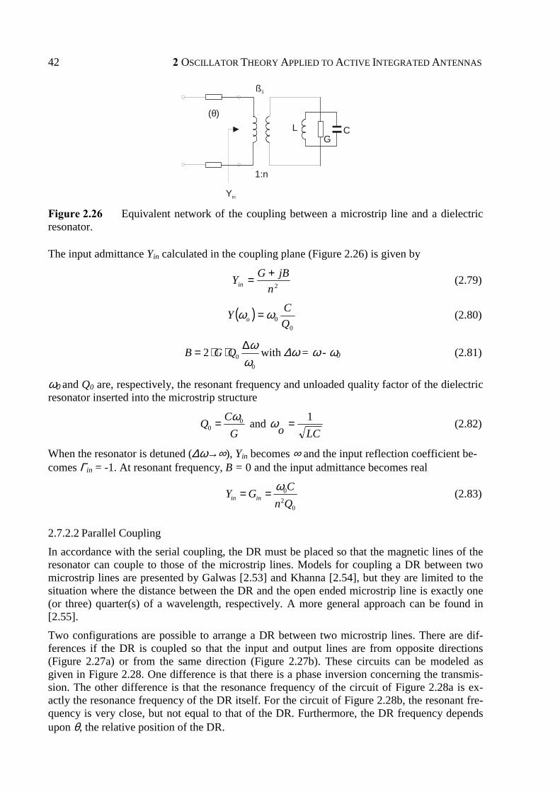
42 2 OSCILLATOR THEORY APPLIED TO ACTIVE INTEGRATED ANTENNAS
ß1
LG
C
(θ)
1:n
Yin
Figure 2.26 Equivalent network of the coupling between a microstrip line and a dielectric resonator.
The input admittance Yin calculated in the coupling plane (Figure 2.26) is given by
2njBGYin
+= (2.79)
( )0
0 QCY o ωω = (2.80)
00
2B G Q ωω∆= ⋅ ⋅ with ∆ω = ω - ω0 (2.81)
ω0 and Q0 are, respectively, the resonant frequency and unloaded quality factor of the dielectric resonator inserted into the microstrip structure
00
CQGω= and
LCo1=ω (2.82)
When the resonator is detuned (∆ω→∞), Yin becomes ∞ and the input reflection coefficient be-comes Γin = -1. At resonant frequency, B = 0 and the input admittance becomes real
02
0in in
CY Gn Qω= = (2.83)
2.7.2.2 Parallel Coupling
In accordance with the serial coupling, the DR must be placed so that the magnetic lines of the resonator can couple to those of the microstrip lines. Models for coupling a DR between two microstrip lines are presented by Galwas [2.53] and Khanna [2.54], but they are limited to the situation where the distance between the DR and the open ended microstrip line is exactly one (or three) quarter(s) of a wavelength, respectively. A more general approach can be found in [2.55].
Two configurations are possible to arrange a DR between two microstrip lines. There are dif-ferences if the DR is coupled so that the input and output lines are from opposite directions (Figure 2.27a) or from the same direction (Figure 2.27b). These circuits can be modeled as given in Figure 2.28. One difference is that there is a phase inversion concerning the transmis-sion. The other difference is that the resonance frequency of the circuit of Figure 2.28a is ex-actly the resonance frequency of the DR itself. For the circuit of Figure 2.28b, the resonant fre-quency is very close, but not equal to that of the DR. Furthermore, the DR frequency depends upon θ, the relative position of the DR.
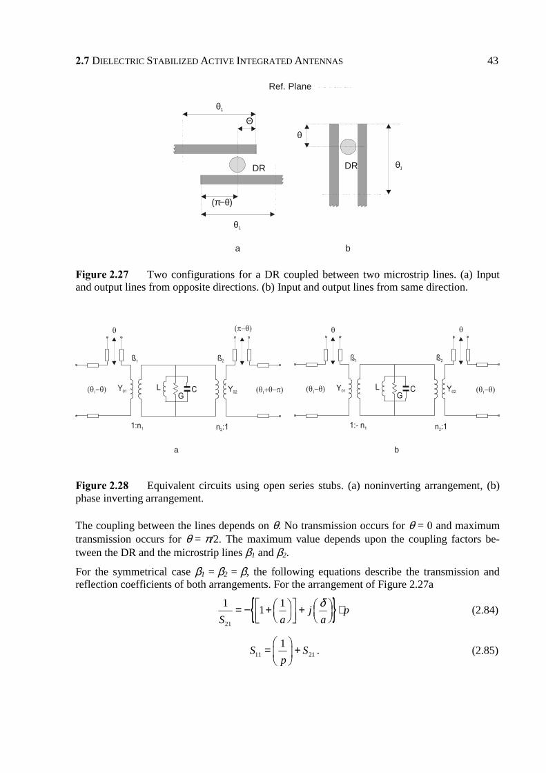
2.7 DIELECTRIC STABILIZED ACTIVE INTEGRATED ANTENNAS 43
Ref. Plane
(π−θ)
θ1
θ1
Θθ
θ1DR DR
ba
Figure 2.27 Two configurations for a DR coupled between two microstrip lines. (a) Input and output lines from opposite directions. (b) Input and output lines from same direction.
a b
Figure 2.28 Equivalent circuits using open series stubs. (a) noninverting arrangement, (b) phase inverting arrangement.
The coupling between the lines depends on θ. No transmission occurs for θ = 0 and maximum transmission occurs for θ = π/2. The maximum value depends upon the coupling factors be-tween the DR and the microstrip lines β1 and β2.
For the symmetrical case β1 = β2 = β, the following equations describe the transmission and reflection coefficients of both arrangements. For the arrangement of Figure 2.27a
21
1 11 j pS a a
δ = − + + ⋅ (2.84)
11 211S Sp
= +
. (2.85)

44 2 OSCILLATOR THEORY APPLIED TO ACTIVE INTEGRATED ANTENNAS
For the arrangement of Figure 2.27b
21
1 11 cotj pS a a
δ θ = + + + ⋅ (2.86)
11 211S Sp
= −
(2.87)
where δ = Q[(f2 / f02)-1], a = 2β sin2θ, the phase factor p = cos2θ1 + jsin2θ1, θ1 is related to the
reference plane distances as shown in Figure 2.27, f0 is the resonant frequency of the DR itself, while Q is the unloaded quality factor in the microstrip environment. Eqs. (2.84) to (2.87) do not include any loss effects and serve only for determining the resonance frequency.
2.7.3 DR Stabilized Active Integrated Antenna Design Based on the layout derived in section 2.1, the DR can be coupled in three different ways. However, since the gate line is frequency determining, only gate line coupling is examined. To ease the design, the impedance of the gate line is changed to 50 Ω, and the line is lengthened by λ/2 allowing easy use of the equations given in section 2.7.2.1.
Knowing the S-parameters of the transistor and the reflection coefficients from the lines con-nected to the drain and source terminal of the transistor, we can predict that the input imped-ance of the gate line together with the DR must be inductive with a very low real part at reso-nance (|Γin|→1). However, the DR coupled to the gate resonator shows band-stop behavior. To achieve high frequency selectivity, Γin must be minimized that corresponds to a ℜ Yin of 50 Ω. This is a contradiction to the required resonance condition making the fulfillment of the oscilla-tion condition impossible. Since the coupling of a DR to a single microstrip line does not im-prove the AIA properties, it is not considered further.
When building a feedback type active antenna, the feedback elements are normally constructed with microstrip lines, which have low-Qs. On the other hand, dielectric resonators have the ad-vantages of small size and high quality factor. Therefore, we tried to use a dielectric resonator as the feedback element for an AIA.
To find the optimal position for the DR feedback, all possible configurations (gate-drain, gate-source, drain-source) were analyzed. The model given in Figure 2.28b was used with the mu-tual impedances set to be 1, assuming optimal coupling, as discussed in [2.51]. The oscillation condition was calculated using linearized oscillator theory (section 2.1). The microstrip was modeled with lumped elements to consider the DR feedback. The distance between the open-ended lines and the DR was chosen in accordance with [2.55] to be θ = π/2. Simulation results show that oscillation occurs only with the DR between the gate and drain lines. For all other configurations, transmission is too weak.
Different AIA layouts were simulated and transmission behavior was modeled based on Eq. (2.86). To couple the DR between the gate and drain lines, they were lengthened to provide enough space available for the DR and to satisfy coupling condition (θ = π/2). A typical AIA layout is shown in Figure 2.29.

2.7 DIELECTRIC STABILIZED ACTIVE INTEGRATED ANTENNAS 45
1 mm
Gate
Source
Drain
DR
Figure 2.29 AIA layout for parallel feedback with a DR.
Figure 2.30 shows the simulated and measured transmission of the test structures with and without the DR. The measured 3 dB bandwidth of the frequency selective feedback (meas w/ DR) of 1 GHz is much wider than estimated in the lossless simulation (sim), which is in accor-dance with literature [2.56]. Impact of the DR on the transmission behavior can be evaluated comparing the measurements with the DR (meas w/ DR) with the measurement without the DR (meas w/o DR). At resonance, the transmission is 28 dB above the coupling without the DR. Losses in the microstrip lines as well as losses trough the DR cause the wide bandwidth.
Losses caused by the DR can be reduced using metal shielding or a tuning plate above the DR. However, using a tuning plate would destroy all desired radiation. Thus, this configuration is not suitable to improve the phase noise. In addition, energy from the gate resonator is coupled into the DR, decreasing the radiated power. Both the gate resonator and the DR compete as ra-diating elements, deteriorating AIA properties. If the open-end of the gate line is replaced by a 50 Ω resistor as proposed in [2.54] and [2.56], the oscillation condition is no longer satisfied (section 2.3.1). Therefore, the parallel feedback loop approach is not optimized since we cannot see any advantages using this design.
20 30Frequency [GHz]
0Tr
ansm
issi
on [d
B]-4
0
meas w/ DR
meas w/o DR
sim
Figure 2.30 Measured and simulated transmission of the DR between the gate and drain lines. The simulated configuration from Eq. (2.86) does not consider loss.

46 2 OSCILLATOR THEORY APPLIED TO ACTIVE INTEGRATED ANTENNAS
2.8 Injection Locking An oscillator is described by several characteristics such as frequency, power, noise, stability, and so forth. Normally, a source is free-running with a random phase unless some mechanism is used to synchronize it. For synchronization, locking bandwidth and locking gain are most im-portant. Locking gain describes the amount of power required to externally lock an oscillator. Locking bandwidth is defined as the frequency locking range for a given relative oscillator power. There are several methods to injection lock a source:
1. Open-cavity resonator
2. External source
3. Mutual coupling (free space waves, surface waves, external circuitry)
Open cavity resonators are not used in this work since we only consider simple uniplanar cir-cuits. Mutual coupling is examined in section 2.9. Here, we discuss the influence of an external source on the AIA behavior. This source can either have the same or a subharmonic frequency. Additionally, modulated optical signals can be used.
2.8.1 Definition The theory introduced in section 2.2 is adapted here for injection locking of a single AIA. The AIA is modeled as a parallel resonant circuit with an independent current source representing the injected signal.
Applying the FFT to the KCL in Figure 2.5, Eq. (2.21) can be adapted as follows
( ) ( ) ( )rL
inj jVG
IAS
QAF ωωµωφ −+
+= 0
0
2, (2.88)
where
( )
−≡ 2
2
1αAAS (2.89)
and
L
L
GGG −
= 0µ (2.90)
Writing the injected signal as
( )ttjLinj
injeGI ψωρ += (2.91)
and using the expression for V(t) derived in section 2.2 gives the oscillation amplitude and phase dynamics
( ) ( ) ( )0 0 cos2 2 inj r
dA A S A tdt Q Q
ω ωµ ρ ω ω ψ φ= ⋅ + − + − (2.92)
( ) ( )00 sin
2r inj rd tdt A Q
ωφ ρω ω ω ω ψ φ= − + − + − (2.93)
In this form ρ, which describes the strength of the injected signal, has the same units as A. Here, it is convenient to choose ωr = ωinj to eliminate the explicit time dependence of the right hand

2.8 INJECTION LOCKING 47
side. In the general case, these coupled differential equations cannot be solved analytically, but if the injected signal is significantly smaller than the free-running amplitude (ρ « A), the steady-state amplitude should remain close to its free-running value, A ≈ α, and Eq. (2.93) is decoupled from Eq. (2.92). The AIA is then described by Adler’s equation [2.57]
( )φψωαρωωφ
ω
−+−=
∆
sin2
00
m
Qdtd
inj (2.94)
This is the key equation for injection locking. If a steady state solution can be found for the phase such that dφ/dt = 0, this indicates that the AIA is synchronized to the injected signal. Solving for the steady state phase difference between the AIA and the injected signal (∆φ = ψ-φ0) gives
∆−
=∆ −
m
inj
ωωω
φ 01sin (2.95)
which indicates that an injection locked solution is only possible when the injected signal fre-quency lies within the “locking range” of the AIA, ω0 ± ∆ωm. The inverse sine function gives two possible solutions for the phase difference in this range; the correct result is found from a stability analysis [2.10].
Eq. (2.51) directly leads to a condition for synchronization since the left side is bounded by ±1. Therefore the condition for synchronization is
0
02ω
ωωαρ injQ
−> (2.96)
The locking range (bandwidth, BWL), which is required to find the maximum ∆ω for which synchronization is maintained, is now given by according to Eq. (2.94)
αρωω
QBW mL
02 =∆= . (2.97)
Writing in terms of power gives [2.58]
P
PQf
f inj1
0
max =∆
(2.98)
From Eq. (2.98), it can be seen that the locking bandwidth of the AIA is inversely proportional to the Q-factor of the resonant circuit and proportional to the square root of the injection power. Eq. (2.98) is only valid for low Pinj since it becomes nonlinear for high Pinj. To the extend that a large locking range is desired in a practical system, low-Q oscillators with large injected signal strength are required on condition that ρ « A.
The presence of an injection-locking signal introduced to an AIA can lead to some very inter-esting effects. It is well known that a low power signal whose frequency lies close to that of a free running AIA can lead to frequency shift and phase noise improvement [2.9]. This signal, known as the injection-locking signal, can be fed directly into a circuit port on the active an-tenna. This leads to a highly controllable situation where features such as external Q-factor of the AIA can be accessed by classical injection locked methods. A second method, which ex-ploits the fundamental nature of the circuit, is to introduce the injection-locking signal by a spa-

48 2 OSCILLATOR THEORY APPLIED TO ACTIVE INTEGRATED ANTENNAS
tially remote source. This technique eases circuit configuration requirements but is more diffi-cult to characterize, particularly in equivalent circuit based computer simulation.
2.8.2 Injection Locked AIA In this work, injection locking is realized by feeding the locking signal into the circuit. This is realized with a capacitance at the end of the gate resonator (Figure 2.31).
1 mm
injectionsignalinput
gate source drain
coupling gap= 300µm
Figure 2.31 Layout of the injection locked AIA.
The length of the coupling gap is chosen long enough so that the AIA remains unperturbed without the injection signal, but also short enough to neglect the phase shift due to the coupling gap. The signal is coupled into the 50 Ω coupling line (left side in Figure 2.31) by means of a thin semi-rigid cable that is routed trough a via hole of the substrate.
Though the phase noise can be improved, the disadvantage of the injection locking approach is that an external locking source is needed. The task of this source can also be fulfilled by another AIA or multiple AIAs. This case is investigated in the following section.
2.9 Coupling and Power Combining Coupled AIAs show synchronization properties that are suitable for millimeter wave power combining, pulse generation, and beam scanning applications. The analysis of multiple AIA systems involves relatively minor extensions of the elementary injection locking theory, but yields significantly more complex and interesting dynamics.
Since robust locking favors a low-Q design, the AIAs having a low-Q microstrip resonator are well suited for coupling applications. In this section, coupling and power combining mecha-nisms for AIAs are described allowing the design and understanding of AIA arrays.
When determining the coupling topology, it is helpful to know the physical coupling behavior between the AIAs to have a first indication of how large the coupling distances are. For this purpose, the load variation is applied. However, with this method, only the coupling between two AIAs can be simulated. This is why in our design the approximate coupling distances be-tween two AIAs are derived first using the load variation method, and then the exact distances between all AIAs in the array are determined with the coupling theory based on nonlinear oscil-lator modeling.
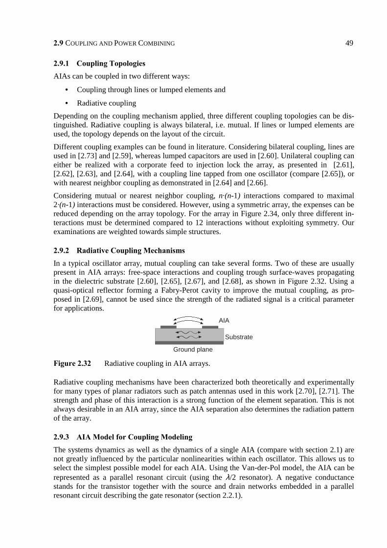
2.9 COUPLING AND POWER COMBINING 49
2.9.1 Coupling Topologies AIAs can be coupled in two different ways:
• Coupling through lines or lumped elements and
• Radiative coupling Depending on the coupling mechanism applied, three different coupling topologies can be dis-tinguished. Radiative coupling is always bilateral, i.e. mutual. If lines or lumped elements are used, the topology depends on the layout of the circuit.
Different coupling examples can be found in literature. Considering bilateral coupling, lines are used in [2.73] and [2.59], whereas lumped capacitors are used in [2.60]. Unilateral coupling can either be realized with a corporate feed to injection lock the array, as presented in [2.61], [2.62], [2.63], and [2.64], with a coupling line tapped from one oscillator (compare [2.65]), or with nearest neighbor coupling as demonstrated in [2.64] and [2.66].
Considering mutual or nearest neighbor coupling, n·(n-1) interactions compared to maximal 2·(n-1) interactions must be considered. However, using a symmetric array, the expenses can be reduced depending on the array topology. For the array in Figure 2.34, only three different in-teractions must be determined compared to 12 interactions without exploiting symmetry. Our examinations are weighted towards simple structures.
2.9.2 Radiative Coupling Mechanisms In a typical oscillator array, mutual coupling can take several forms. Two of these are usually present in AIA arrays: free-space interactions and coupling trough surface-waves propagating in the dielectric substrate [2.60], [2.65], [2.67], and [2.68], as shown in Figure 2.32. Using a quasi-optical reflector forming a Fabry-Perot cavity to improve the mutual coupling, as pro-posed in [2.69], cannot be used since the strength of the radiated signal is a critical parameter for applications.
AIA
Substrate
Ground plane
Figure 2.32 Radiative coupling in AIA arrays.
Radiative coupling mechanisms have been characterized both theoretically and experimentally for many types of planar radiators such as patch antennas used in this work [2.70], [2.71]. The strength and phase of this interaction is a strong function of the element separation. This is not always desirable in an AIA array, since the AIA separation also determines the radiation pattern of the array.
2.9.3 AIA Model for Coupling Modeling The systems dynamics as well as the dynamics of a single AIA (compare with section 2.1) are not greatly influenced by the particular nonlinearities within each oscillator. This allows us to select the simplest possible model for each AIA. Using the Van-der-Pol model, the AIA can be represented as a parallel resonant circuit (using the λ/2 resonator). A negative conductance stands for the transistor together with the source and drain networks embedded in a parallel resonant circuit describing the gate resonator (section 2.2.1).

50 2 OSCILLATOR THEORY APPLIED TO ACTIVE INTEGRATED ANTENNAS
Knowing that the complete microstrip structure radiates thus having influence on the coupling behavior, only the gate resonator must be taken into consideration. Based on the current distri-bution of the planar structure, the coupling behavior of the complete structure can be calculated. Based on these results, it can be shown, that the gate resonator dominates by far the radiation, i.e. coupling performance. There is only a negligible error if the remaining structure is not con-sidered for coupling.
2.9.4 Radiative Coupling Modeling If a parallel resonant circuit is loaded with an active device (Figure 2.5), steady state is de-scribed by
LLdd jBGjBG −−=+ (2.99)
where Gd,L and Bd,L are device and circuit conductances and susceptances, respectively, at reso-nance at the plane between the transistor and the circuit.
To simulate an array with strong coupling, the load variation method can be used. Instead of examining two antennas, a metal sheet is used to generate an image of the AIA. This situation is modeled with a lossy transmission line so that the input admittance looking in the gate resona-tor can be described as [2.72]
2
00 0 2
0
11
d
C L d
eY G j C Ye
γ
γ
ωω ρωω ω ρ
−
−
−= + − + +
(2.100)
where ρ is the reflection coefficient of the reflector when coupled through a transmission line of characteristic impedance Y0. Here γ = (α + jβ) is the propagation constant, α is the attenuation constant per unit length, β is the wave number, d is the distance between the AIA and the reflector, ω = ω0+∆ω where ω0 is the free running frequency and ∆ω is the induced frequency shift due to load coupling. Since a metal sheet is used for imaging, its reflection coefficient ρ is set equal to –1. Substituting this into Eq. (2.100) with Bd +BL = 0, i.e. the resonant condition, the following expression can be derived:
( ) ( )( ) ( )[ ]2 2
0
sin cos2 sin sinhe
K d dQ d d
β ϕ β ϕωω β ϕ α ϕ
+ ∆ + ∆∆ =+ ∆ + ∆
(2.101)
Here Qe is the external Q-factor of the AIA (section 2.6). The proportionality factor K has been introduced to account for any mismatch and or coupling loss that may exist between the resona-tor and the modeled transmission line.
Regarding surface waves, only the TM0 mode must be considered since this is the only mode without a cut-off frequency. The cut-off frequency of the next higher TE0 mode in the alumina substrate is 99.2 GHz and the substrate wavelength for the used thickness is the free-space wavelength (see [2.42]). The wave numbers of the wave in the substrate and in air are the same for this case.
Regarding Figure 2.34, it can be seen that coupling is exploited in two different directions, whereas the antenna is linear polarized. One must differentiate between E- and H-plane cou-pling with respect to the field distribution of the resonator (Figure 2.34). To consider the differ-ent couplings, the occurring phase shift is compared with the theoretical phase shift. This phase difference ∆ϕ -based on the consideration of E- and H-planes, different coupling forms (free space and surface waves) and the finite dimensions of the resonator- is calculated based on full-wave simulations and inserted into Eq. (2.101).

2.9 COUPLING AND POWER COMBINING 51
E- and H-plane simulations give two different curves predicting the changes of the free-running frequency as a function of separation between the AIA and its image (Figure 2.33). The fre-quency changes are only theoretical values, since different line admittances result in different transistor operation conditions, which is not taken into consideration here. However, it is an effective tool to calculate the distances between the AIA elements for optimum coupling.
The two curves depicted in Figure 2.33 give a first insight in the coupling behavior of the array. H-plane coupling for a distance of 1.5 mm depends strongly on the element separation whereas E-plane coupling for a distance of 2 mm is less dependent. The distances from this calculation are used as the starting point for the design of the AIA array.
Distance between neighboring AIA's [mm]
Rel
ativ
e fre
quen
cy c
hang
e
E
H
Figure 2.33 Simulated changes in the free running frequency of the AIA array vs. element separation for E- and H-plane coupling.
2.9.5 Coupling Theory A general model for the analysis of coupling phenomena is presented in [2.16] and [2.73] and is shown in Figure 2.19. Each oscillator circuit is coupled to an N-port network, which is de-scribed in terms of Y-parameters. The N-port network includes both coupling circuits and the load.
Applying this model to the examined AIA, the AIA must be split up between the gate resonator and the transistor with the drain and source networks (section 2.2). This approach is not obvi-ous, since the radiation behavior of the AIA cannot be understood by inspection. However, the validity of this approach can be proved by investigating the radiation and coupling behavior of the complete AIA based on full-wave analysis (chapter 3). From these results, it can be seen that the coupling behavior is dominated by the gate resonator, and the influence of the remain-ing network can be neglected.
With section 2.3.4 and Figure 2.19, we can write applying linear network theory
( ) ( )=
=N
j i
jijiL V
VYY
1, ~
~ωω (2.102)

52 2 OSCILLATOR THEORY APPLIED TO ACTIVE INTEGRATED ANTENNAS
where N is the number of oscillators in the system. In addition
( ) ( ) ( ), ,1
,N
inj i t ij i jj
I Y V Vω ω ω=
= (2.103)
where
( ) ( ) ( ), ,, ,t ij i osc i i ij ijY V Y V Yω ω δ ω= + (2.104)
and δij is the Kronecker delta.
Applying the inverse Fourier transformation and exploiting the slowly varying amplitude and phase assumptions, Eq. (2.103) can be transformed according to [2.16] to a coupled set of dif-ferential equations
( )
1' 'r
t j ttinj
d edt j
ωδδ ω
−
−
= ⋅ − ⋅
V Y I Y V (2.105)
where tY is a matrix with elements Yt,ij, Iinj is a vector with elements Iinj,i(t), and V’ is a vector with elements Vj’ (the phasor port voltages). This in turn can be expressed as
( )'
' , 1, ,ii i
dV F V i Ndt
= =V (2.106)
where
( )( )
1'
,,' '1 1
N Nt inj j ki t jk
j ki iij
I VF Yj V V
δδ ω
−
= =
= −
YV (2.107)
This can be solved for the amplitude and phase variations by separating real and imaginary parts to give
( ) Re ,ii i
dA A Fdt
= A φ (2.108)
( ) Im , , 1, ,ii
d F i Ndtφ = =A φ (2.109)
This is a general result for analysis of amplitude and phase dynamics in coupled oscillator sys-tems. The analysis can be simplified further by restricting attention to “broadband” coupling networks, which satisfy
( ) ( ) ijioscijt
jY
jY
δωδ
δωδ
δ ,, ≈ (2.110)
in other words, coupling networks that have negligible frequency dependence near the opera-tion frequency. This is equivalent to saying that the oscillator Q-factor is the dominant Q of the system. With this assumption, Fi in Eq. (2.107) is given by
( ) ( )( ) ( ) ( )
−−
≈
=
−
'i
'
1,'
,1
,
V,
, jN
jrijiriosc
i
iinjiriosci
VYAY
VI
jAY
F ωωωδ
ωδV (2.111)
For coupling applications, the steady state is the most interesting. Steady state occurs when the AIAs are synchronized to the same frequency, which is true for

2.9 COUPLING AND POWER COMBINING 53
Nidt
danddt
dAi
ii ,,1,0 =−== ωωφ (2.112)
In this case, the oscillator phases is bounded in time if the reference frequency is chosen to be ω=ωr, in which case the steady state solutions are determined by the set of nonlinear algebraic equations
( ) NiFi ,,1,0 ==φA, (2.113)
If externally injected signals at frequency ωinj are present, the synchronized frequency (and ref-erence frequency) can be taken as ω = ωinj = ωr. However, in the absence of externally injected signals, (Iinj = 0 for all i) the steady state synchronized frequency is not known a priori and must be determined from Eq. (2.113). The real and imaginary parts of Fi must equate separately to zero, so Eq. (2.113) represents a set of 2N equations.
Unless the oscillators are strongly coupled, the oscillation amplitudes remain close to the free-running state. Assuming this is the case, the amplitude and phase dynamics are uncoupled, to first order. Then, we can restrict attention to the phase dynamics governed by Eq. (2.17). This simplifies the analysis considerably.
2.9.6 Theory Applied to the Free Running AIA Array In this work, the AIAs are coupled without any synchronizing signal so that Eq. (2.111) can be simplified to:
( ) ( )( ) ( ) ( )
−−
≈
=
−
'i
'
1,
1,
V,
, jN
jrijiriosc
iriosci
VYAY
jAY
F ωωωδ
ωδV (2.114)
To solve this equations, only the port voltages Vi’ and Y-parameters must be determined. If the amplitudes remain close to their free-running state and the AIAs have reproducible characteris-tics, the port voltages are the same for all AIAs. Based on simulations within the considered frequency range, we can also determine the derivative of the admittance Yosc. This is why two simplifications can be made:
1V'
i
'
=jV and (2.115)
( )( ) 0
, 1, ≠
−
ωδωδj
AY iriosc (2.116)
Finally, steady state can be determined using (2.17) and (2.114) leading to:
( ) ( )=
=−N
jrijiriosc YAY
1, , ωω (2.117)
Only Y-parameters are needed to solve the steady state condition for the free-running AIA array Eq. (2.117). Recalling that the amplitudes remain close to their free running state, the amplitude dependence in Eq. (2.117) can be neglected. Yij, the admittances of the coupling network, de-pend on the coupling structure and can either be measured or simulated.
Considering the arrangement of the AIAs within the array, it is symmetric, whereas the orienta-tion of the AIAs is chosen to allow optimal coupling in both x- and y-direction. The layout of the 2×2 array as starting point of the experimental optimization is shown in Figure 2.34.

54 2 OSCILLATOR THEORY APPLIED TO ACTIVE INTEGRATED ANTENNAS
E: 2 mm
H: 1.5 mm
RGS RGS
RGSRGS
Ya
Yb
YcYd
Figure 2.34 Layout of the 2×2 array as starting point of the experimental optimization.
The coupling network can be described by a 4×4 admittance matrix. Considering the arrange-ment in Figure 2.34, it can be written as:
=
abcd
badc
cdab
dcba
YYYYYYYYYYYYYYYY
Y (2.118)
Ya is the input admittance of the gate resonator, whereas Yb with Yd represent the coupling ad-mittances between two resonators as depicted in Figure 2.34. Comparing Eq. (2.118) with Eq. (2.117), it can be seen that Eq. (2.117) must be solved for only one AIA to get the solution for the complete array.
The coupling admittances are determined based on the coupling topology applied. We start the simulation with the topology derived from section 2.9.4. (dE = 2 mm, dH = 1.5 mm). To derive the admittances of the coupling network, the calculation can be simplified considerably if only the gate resonators are considered. This approximation is justifiable since the gate resonator dominated the radiation, i.e. coupling behavior by far (chapter 3). Therefore, the coupling be-tween the gate resonators is calculated using full-wave analysis.
After calculation, the admittances are inserted into Eq. (2.117). This is shown in Figure 2.35 separately for the real and imaginary part.
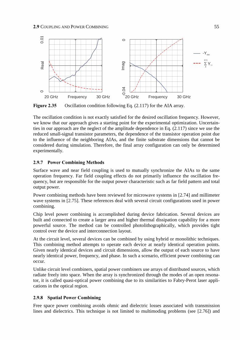
2.9 COUPLING AND POWER COMBINING 55
20 GHz 20 GHzFrequency Frequency30 GHz 30 GHz-0.0
40
00.
01R
eal
Imag
-Yosc
n=1
4
Figure 2.35 Oscillation condition following Eq. (2.117) for the AIA array.
The oscillation condition is not exactly satisfied for the desired oscillation frequency. However, we know that our approach gives a starting point for the experimental optimization. Uncertain-ties in our approach are the neglect of the amplitude dependence in Eq. (2.117) since we use the reduced small-signal transistor parameters, the dependence of the transistor operation point due to the influence of the neighboring AIAs, and the finite substrate dimensions that cannot be considered during simulation. Therefore, the final array configuration can only be determined experimentally.
2.9.7 Power Combining Methods Surface wave and near field coupling is used to mutually synchronize the AIAs to the same operation frequency. Far field coupling effects do not primarily influence the oscillation fre-quency, but are responsible for the output power characteristic such as far field pattern and total output power.
Power combining methods have been reviewed for microwave systems in [2.74] and millimeter wave systems in [2.75]. These references deal with several circuit configurations used in power combining.
Chip level power combining is accomplished during device fabrication. Several devices are built and connected to create a larger area and higher thermal dissipation capability for a more powerful source. The method can be controlled photolithographically, which provides tight control over the device and interconnection layout.
At the circuit level, several devices can be combined by using hybrid or monolithic techniques. This combining method attempts to operate each device at nearly identical operation points. Given nearly identical devices and circuit dimensions, allow the output of each source to have nearly identical power, frequency, and phase. In such a scenario, efficient power combining can occur.
Unlike circuit level combiners, spatial power combiners use arrays of distributed sources, which radiate freely into space. When the array is synchronized through the modes of an open resona-tor, it is called quasi-optical power combining due to its similarities to Fabry-Perot laser appli-cations in the optical region.
2.9.8 Spatial Power Combining Free space power combining avoids ohmic and dielectric losses associated with transmission lines and dielectrics. This technique is not limited to multimoding problems (see [2.76]) and

56 2 OSCILLATOR THEORY APPLIED TO ACTIVE INTEGRATED ANTENNAS
allows the combination of a greater number of devices as presented in [2.68]. Since spatial and quasi-optical power combining occurs in space, high combining efficiencies (close to 100%) are possible with AIAs. Consequently, active antenna research was originally spurred on for the purpose of spatial power combining. Power combining at microwave and millimeter-wave re-gions is feasible with AIAs. Spatial power combining methods also relax fabrication tolerances and reduce the overall cost of millimeter and sub-millimeter wave systems. Spatial power com-biners radiate freely as large planar arrays of synchronously oscillating sources to produce a single large power output at some point in space. Spatial power combining methods enable AIA arrays to operate as one coherent transmitter with predictable effective radiated power, beam width, and tuning bandwidth.
The individual free running AIAs must be injection locked via mutual coupling, external feed-back, coupling networks, or an external source (section 2.9.1). Spatial power combiners have been demonstrated using distributed oscillators in [2.62] and amplifiers in [2.77]. Spatial power combiners can be modeled directly with planar array theory as demonstrated in [2.58]. The ra-diation behavior of the array is discussed in chapter 3.
3 CIRCUIT AND DEVICE MODELS AND THEIR IMPLEMENTATION FOR AIA DESIGN
In this chapter, the semiconductor devices and their modeling are described, followed by the theoretical background of numerical circuit and antenna simulation. The theory behind the models used in our AIA design is given for completeness, but also for assessing the errors and explaining the approximations used.
When deriving a model, it must be considered that the AIA consists of two fundamental differ-ent parts that have to be treated separately. The active device can be modeled based on meas-ured parameters (behavioral) or a large-signal (physical) model can be used. The embedding microstrip structure can be described on the circuit level (behavioral) or based on full-wave simulations (physical).
AIA with different semiconductor devices are designed, fabricated, and compared to show the universal nature of the design procedures. The AIAs worked equally well with commercial HEMT devices (by Infineon) and research lab devices (by DaimlerChrysler). The goal of this chapter is to show that any device of the future can be used while the design technique remains the same.
3.1 Semiconductor Devices for Integrated Antennas
3.1.1 Two-Terminal Devices In the AIAs presented here, the two-terminal device that was used in the VCO is a varactor di-ode. In the VCO application, the diode is reversed biased and behaves to first order like a volt-age variable capacitance. A varactor diode can be either a silicon or GaAs diode. The main dif-ference between silicon and GaAs is that a higher Q can be obtained form GaAs devices. This is due to the lower resistivity of GaAs for a given doping level. GaAs devices have a higher ther-mal resistance than silicon devices resulting in significantly larger settling times.
For high frequencies, diode behavior is dominated by the junction capacitance cj. Since this capacitance depends on the length of the space charge region i.e. the reverse-bias voltage, it is a voltage controllable capacitance and can be expressed by
m
j
jdj
vv
ccc
−+=
1
0 (3.1)
where cd (small-signal capacitance) and vj (junction potential) are given, m is the junction expo-nential factor, cj0 (zero bias junction capacitance) is derived from small-signal measurements, and v is the diode voltage. For a linearly graded junction, m=1, and for a hyperabrupt junction, m>1, up to 1.5. We used a GaAs hyperabrupt Alpha diode GMV9821-000. Aside from m, an-

58 3 CIRCUIT AND DEVICE MODELS AND THEIR IMPLEMENTATION FOR AIA DESIGN
other important parameter is Rs that limits the Q. Typical values are m=1.25, cj0=2.78 pF, vj=1 V, and Rs=5.14 Ω. Figure 3.1 shows the simulated and measured input reflection coefficients of the shunted varac-tor for Udiode = -1 V (Traces A and B) and Udiode = -13 V (Traces C and D).
20 GHz Frequency 30 GHz
U =-1VDiode
U =-13VDiode
s m
sm
Figure 3.1. Measured and simulated input reflection coefficients of the shunted varactor for Udiode = -1 V (Traces A and B) and Udiode = - 13 V (Traces C and D).
3.1.2 IMPATT Diodes Considering frequencies above 30 GHz, transistors cannot be used as active devices in AIAs due to their low gain at these frequencies. For some applications, however, it is necessary to have antennas with short wavelengths. IMPATT diodes are well established in AIAs for fre-quencies up to 76 GHz as presented in [3.1].
These diodes are biased above the threshold for impact ionization. The carrier generation in connection with the transit time delay causes a dynamic negative resistance. Since the high-field drift velocity of Si and GaAs are in the same order, silicon is suited for IMPATT diodes as well as GaAs.
The negative real part of the IMPATT diode impedance is in the range of 1-10 Ω. For this rea-son, a low impedance termination of the IMPATT diode is required in order to achieve oscilla-tor operation. Modeling and the AIA design based on IMPATT diodes is not considered in this work. A good review of existing AIA based on these diodes can be found in [3.2]. IMPATT based AIAs are applied here in Fabry-Perot resonators and used in automotive crash sensors (chapter 5).
3.1.3 Three-Terminal Devices Though AIAs can be realized with two- or three-terminal devices, the AIAs developed in this work are based on transistors due to their better DC-to-RF efficiency. Both high electron mobil-ity transistors (HEMTs) and heterojunction bipolar transistors can be used. Both belong to the class of III-V semiconductor devices using heterojunctions for their operation.
HBTs are vertical devices with inherent temperature instability, i.e. the current increases with temperature, causing thermal runaways. Resistive biasing that provides negative feedback is

3.1 SEMICONDUCTOR DEVICES FOR INTEGRATED ANTENNAS 59
therefore necessary for HBTs. HEMTs do not have a positive current temperature coefficient and are easier to bias. They are also easier to match to, as HBTs have very low reactive input impedance.
Few HBTs are commercially available, and in this work, we use a commercial HEMT and a research HBT. We had a small-signal model for the HEMT and an in-house developed large-signal model for the HBT.
3.1.3.1 High Electron Mobility Transistors
The t409 Infineon HEMT devices presented in [3.3] and used in the AIAs are built from epi-taxial layers grown by MBE using a photolithography of 0.5 µm and SiN spacer layers to result in a gate length of 0.25 µm.
The chip layout with a total gate width of 4·45 µm is called t409 and is shown in Figure 3.2. The inner sources are connected via a low inductance and parasitic capacitance source over drain and gate air-bridge. Two bond pads are available on each of the two source sides for low feedback connection at high frequencies in common source configuration. In addition, two gate pads are used for gate bonding for low phase loss at high frequencies. For the drain connection, only one pad is necessary. The chip size is 300 µm*350 µm less the loss from sawing. Figure 3.2 shows the chip layout of the used HEMT. The gold contacts have a diameter of 55 µm and can be connected with either wedge or flip-chip bonding.
source source
drain
gate
airbridge
55 µm
40 µm
300
µm
350 µm
Figure 3.2. Photography of the t409d chip.
3.1.3.2 Heterojunction Bipolar Transistors
The heterojunction bipolar transistor (HBT) is a modified bipolar transistor that relies on the use of heterojunctions for its operation. In the HBT, the emitter and base are formed in semi-conductors with different band gaps. The emitter is in the wider band gap material. High emitter injection efficiency can be maintained even with heavy base doping (to reduce base spreading resistance) and light emitter doping (to reduce base emitter junction capacitance), see [3.4]. Figure 3.3 shows a scanning electron micrograph (SEM) of the used six fingers SiGe HBT manufactured by DaimlerChrysler. The resulting SiGe-HBTs exhibit ft values up to 70 GHz and

60 3 CIRCUIT AND DEVICE MODELS AND THEIR IMPLEMENTATION FOR AIA DESIGN
fmax,MAG values up to 95 GHz. The maximum current capability of this type with six emitter-fingers reaches about 50 mA; the breakdown-voltage exceeds 5 V(details see [3.5]).
10 µm
Emitter
Emitter
Collector
Base
Figure 3.3 Scanning electron micrograph of the six fingers SiGe HBT.
3.2 Transistor Modeling for Active Integrated Antennas For linear (behavioral) modeling of the active device, measured S-parameters are typically used. The device is described as a black box containing measured two-terminal or analytically calculated three-terminal S-parameters. Sometimes, a small-signal model is derived from the measured parameters.
Large-signal characterization (physical modeling) is an important requisite since it is only under this operation condition that the power producing oscillator action of the AIA will reach a sta-ble limit circle. The derivation of a large-signal model for the active device such that they pro-vide a realistic estimation of the nonlinear performance is a subject of intense research.
Both linear and nonlinear transistor models are presented here. As demonstrated in chapter 2, prediction of the oscillation frequency can be achieved using a linearized model. If the power level and the harmonic behavior are required in addition, nonlinear models are needed.
3.2.1 S-Parameter Description The transistor (three-terminal device) is generally characterized by its two-port S(2)-parameters with one of its ports grounded and the others assumed to be terminated with the port character-istic impedance, usually 50 Ω. Figure 3.4 shows the description of the transistor as a two-port device. This configuration is used for two-port S-parameter measurements. The two-port S-parameter matrix of the transistor can be written as:
⋅
=
2
1)2(
22)2(
21
)2(12
)2(11
2
1
aa
SSSS
bb
(3.2)

3.2 TRANSISTOR MODELING FOR ACTIVE INTEGRATED ANTENNAS 61
Transistor
Port 1 Port 2
GND
Gate Drain
Source
[S ](2) a2a1
b2b1
Figure 3.4 Transistor as a two-port device.
The use of three-port S-parameters has not often been used due to the complexity of the analy-sis involved. It eliminates the otherwise necessary conversion to and from Z- and Y-parameters to analyze the series and parallel feedback effects. In the AIA design of this work, the use of the three-port S-parameter matrix is essential. The transistor shown as a three-port device is shown in Figure 3.5, and the S-matrix of the incident and reflected waves is given by:
⋅
=
3
2
1
333231
232221
131211
3
2
1
aaa
SSSSSSSSS
bbb
(3.3)
The ports 1, 2, and 3 represent gate (base), drain (collector), and source (emitter), respectively. This indefinite three-port matrix satisfies the following conditions
=
=3
1
1j
ijS (3.4)
for i=1, 2, 3 and
=
=3
1
1j
ijS (3.5)
for j=1, 2, 3
Transistor
Port 1 Port 2Gate Drain
Source
Port 3
[S ](3) a2a1
a3
b2b1
b3
Figure 3.5 Transistor as three-port device.

62 3 CIRCUIT AND DEVICE MODELS AND THEIR IMPLEMENTATION FOR AIA DESIGN
The three-port S-parameters of the transistor can be measured directly or obtained analytically from the commonly supplied two-port S-parameters. Typically, these parameters are measured in a common source configuration using a network analyzer. Either the transistor can be con-nected directly to CPW on-wafer probe tips or a special measurement setup must be applied. The HBT layout allows direct contact of the probe tips whereas the HEMT needs a CPW test structure.
After measuring the two-port parameters, they can be transformed into three-port parameters under the assumption that Kirchhoff’s laws are valid for the transistor i.e. it is considered to be lumped: If, for example port 3 of the transistor in Figure 3.5 is connected to ground making a common source (emitter) configuration, then
33
3
1ab
Γ = = − . (3.6)
where Γ3 is the reflection coefficient of port 3. From Eq. (3.3) comes
3132121111 aSaSaSb ++= (3.7)
3232221212 aSaSaSb ++= (3.8)
3332321313 aSaSaSb ++= . (3.9) Using Eq. (3.6) in Eqs. (3.7) and (3.9), and eliminating a3 and b3, yields:
=
+−
+−
+−
+−
= MM
MMM
SSSS
SSS
SSSS
S
SSSS
SSSS
2221
1211
33
322322
33
233121
33
321312
33
311311
11
11S (3.10)
where SM is the S-parameter representation of the two-port measurements and corresponds to Eq. (3.2). Eq. (3.10) represents four equations that form together with the six equations from Eqs. (3.4) and (3.5) 10 equations, which must be solved to find all nine three-port S-parameters. The final relationships that convert a given two-port S-matrix SM into an indefinite three-port matrix are as follows (compare [3.6]):
==
==
−=
2,12,1
2,12,1
33 4ji
Mij
ji
Mij
S
S
S
(3.11)
( )MM SSSS 2212
3332 1
21 −−+=
(3.12)
( )MM SSSS 2221
3323 1
21 −−+=
(3.13)
33
32232222 1 S
SSSS M
++=
(3.14)
332313 1 SSS −−= (3.15)

3.2 TRANSISTOR MODELING FOR ACTIVE INTEGRATED ANTENNAS 63
323331 1 SSS −−= (3.16)
323312 1 SSS −−= (3.17)
232221 1 SSS −−= (3.18)
312111 1 SSS −−= (3.19)
In contrast to low-frequency modeling, S-parameters are used at microwave frequencies rather than equivalent circuit models because the number of fitted parameters (including all parasitics) is very large. It is therefore difficult to derive a good model. For large-signal (time-domain) analysis, there is no option, and therefore large-signal modeling is presented here.
3.2.2 Large-Signal Modeling Large-signal characterization is an important requisite. The AIA will reach a stable limit cycle only under this operation condition. Thus, any quantitative assessment of the behavior of the AIA depends on an intimate knowledge of the subtle interactions between the device and the circuit. The derivation of these models such that they provide a realistic estimate of the large-signal performance is a subject of intense research, e.g. [3.7].
In this work, large-signal modeling is limited to the SiGe HBTs because no model was avail-able for the HEMTs we used. Large-signal modeling of HEMTs is discussed in literature [3.8].
For the large-signal modeling of the HBTs, a VBIC model presented in [3.9] is used. To de-scribe the entire transistor structure, including measurement pads and connecting elements, it is embedded into a network of parasitic capacitances, inductances, and resistors. Compared to standard BJT models, the advantages of this model with respect to our application are mainly a modified Kull-model for quasisaturation, which is used to describe high current effects, a flexi-ble and well suited temperature mapping and the inclusion of self-heating effects. Parameter extraction is based on temperature dependent DC-measurements and bias dependent S-parameter measurements (see [3.10]). In a first step, the parasitic elements are characterized using open and short dummy structures as well as hot and cold device measurements. After the extraction of the junction capacitances, Early voltages are determined. The base- and transport current parameters are extracted from forward and reverse Gummel plots. After that, the tem-perature parameters as well as the thermal impedance are extracted. The key temperature model parameters are effective band gap values for base, emitter, and collector of the HBTs as well as the thermal resistance. High current effects are first modeled with respect to the DC-behavior. After the determination of the transit time parameters, the charge parameters of the high current model are adjusted. For the usable range of bias conditions of the HBTs an excellent fit of simulated to measured data has been achieved for frequencies from DC to 40 GHz. As an ex-ample, Figure 3.6 shows a comparison of simulated and measured output characteristics at both forced base currents as well as forced base-emitter voltages.

64 3 CIRCUIT AND DEVICE MODELS AND THEIR IMPLEMENTATION FOR AIA DESIGN
0
10
20
30
40
50
0.0 1.0 2.0 3.0 4.0Vce [V]
i c [m
A]
ib = const.
0
20
40
60
80
0.0 1.0 2.0 3.0 4.0Vce [V]
i c [m
A]
vbe=const.
Figure 3.6 Comparison of measured (dots) and simulated output characteristics for con-stant base currents and constant base-emitter voltages.
As far as we know, the large-signal model presented in [3.7] is the only large-signal model that describes all existing effects exact enough so that it can be used up to 24 GHz.
3.3 Circuit Simulation Methods Behavioral modeling of microstrip structures can be realized with circuit based models. Within these models, microstrip lines are considered as circuit elements, and the complete microstrip structure is put together from single elements.
Applying these models, fast simulation results can be achieved whereas the accuracy depends on the environment where the models are used. Building the AIA circuit from these models, optimization algorithms can be applied, which is not possible using full-wave analysis.
In this section, circuit based microstrip models and their usability for AIA designs are dis-cussed.
3.3.1 Equivalent Circuits for the Microstrip Lines Microstrip lines as transmission media can be described with closed form expressions. Using these expressions, it must be distinguished between discontinuities, bends, and junctions since they need careful characterization to enable derivation of reliable equivalent circuits.
The purpose of many microstrip models is to provide an equivalent circuit for a given structure. The simplest model is a lumped RLC structure valid at low frequencies or narrow bands. Re-garding larger bandwidths at high frequencies, the circuit cannot be represented anymore by a lumped RLC structure.
Equivalent circuit models represent a more accurate description for microstrip lines. These models are based on expensive research dealing with the line properties and give closed-form expressions that lead to scattering matrixes. Today, these models can be found in microwave software libraries, e.g. [3.11], [3.12]. For more complex structures, these models can be com-bined. To this end, the scattering matrix representation is transformed to the generalized circuit constants matrix (ABCD) that allows easy cascading by multiplying the matrixes. After calcula-tion of the complete structure, the ABCD representation is transformed back to S-parameters. Using the library elements, discontinuities, transmission lines, and radiating elements are treated separately. Though the usage of these models allows very fast design procedures, the dynamic behavior of the fields (coupling, surface waves) is supposed to be negligible. Thus, the

3.3 CIRCUIT SIMULATION METHODS 65
advantages coming with miniaturization are wasted. Furthermore, due to the direct relationship between the current distributions and the fields, using single elements instead of considering the complete circuit does not allow the calculation of far-fields.
Within the range of circuit parameters, often given in terms of line width as a ratio of wave-length, frequency, and substrate parameters, the accuracy may be better than a few percent. Outside these parameters, the discontinuity behave in an anomalous way, due, for instance, to the generation of higher order modes within wide transmission lines or surface waves in thick substrates. Choice of discontinuity model is not always clear and must be confirmed with measurements.
The microstrip line is considered as a lumped element so that no coupling between other ele-ments is modeled and must be taken into consideration with extra coupling models. The reac-tive effects at the line connections are not modeled with these models. However, in many cases, this overall model is sufficient to predict the frequency behavior within a tolerance of few per-cent.
3.3.2 Equivalent Circuits for Microstrip Antennas/Resonators Within an AIA, the microstrip lines are responsible for the frequency determining and radiation properties. Thus, the design of the resonator/antenna element is of special importance for the antenna functionality.
In accordance with non-resonant lines, microstrip antennas/resonators can also be described in different ways. They can be modeled with varying degrees of accuracy. Each modeling strategy gives rise to different physical insights about the problem.
Planar resonators can be represented close to resonance by a resonant circuit. Narrow band-width equivalent circuits are useful for single frequency situations such as frequency estimation for AIAs. They are also very helpful regarding situations where many AIAs are considered to-gether, i.e. AIA arrays, chapter 2. They are limited, however, when used for time domain analy-sis or calculation of spectral performance.
Regarding the models coming with design software, the simplest approach involves represent-ing the antenna element as a very wide (low impedance) section of length L. Here the patch edges and ground plane represent the radiating apertures for the antenna. Thus, the antenna is viewed according to [3.13] in sections of transmission lines normally about one half-wavelength long. The fringing fields can either be modeled with lumped capacitors or with “open-ended transmission lines” incorporating the fringing fields effects (Figure 3.7). This class of model, however, does not take into account higher modes, which degrade cross-polarization levels. Figure 3.7 shows two possible representations of a microstrip resonator based on a reso-nant circuit (a) and combination of multiple line models (b).
LG
C
a b
Figure 3.7 Circuit representations of a microstrip resonator.
66 3 CIRCUIT AND DEVICE MODELS AND THEIR IMPLEMENTATION FOR AIA DESIGN
Using harmonic balance synthesis (chapter 2), simulation accuracy can be improved by increas-ing the number of harmonics involved in the simulation. For this purpose, passive structure simulation at the harmonic frequencies is required on the expense of increased simulation time. Applying linear circuit models, only few harmonics can be modeled due to the restrictions of the build-in models. Our examinations show however, that the usage of the second harmonic is sufficient to predict oscillation frequency within the average simulation tolerance.
Some CAD simulation tools [3.13] also use the cavity model, which is not considered in this work.
3.4 Full Wave Analysis in the Frequency Domain To model the AIA behavior, we divide between the active device and the microstrip structure. The modeling of the transistor is described in section 3.2. In this section, the behavior of the microstrip structure is discussed.
Here, the microstrip circuit is calculated using a global electromagnetic approach in the fre-quency domain. It uses the electric field integral equation (EFIE) solved by the method of mo-ments (MoM). This technique has shown excellent accuracy in the study of a wide range of passive planar circuits and antennas (see [3.1] and [3.14]). In this work, this technique is ap-plied using the efficient and accurate numerical electromagnetic solver “Momentum” supplied by Agilent. With the help of this software, the complete microstrip circuit is simulated as a unity, allowing the consideration of coupling, dispersion, surface waves, and loss effects (radia-tion, dielectric and conductor losses), as well as the calculation of the radiation pattern. The correct use of the simulation software requires the understanding of the numerical algorithms.
3.4.1 Integral Equation Formulation The calculation of the electric current distribution on planar passive structures represents a boundary value problem that can be evaluated using the following conditions:
• The calculation is based on the Maxwell’s equations that are represented as a partial dif-ferential equation system of the second order.
• All relevant solutions of the differential equations fulfill the physical boundary condi-tions of the field vectors (e.g. metallization surface).
• The considered structure is radiating at infinity and there is no incoming wave from in-finity (Sommerfeld’s radiation condition, see [3.15]).
The geometry of the general structure to be analyzed is a multilayer planar multiport network. The distributed part can consist of metallic strip printed over dielectric layers, slots in partial ground planes located at different interfaces and vertical strips and wires that could connect different metallic interfaces. In this work, we consider only the case of a uniplanar, single layer microstrip structure. We assume that we have an infinite dielectric substrate with infinite ground metallization and a definite metallization structure on the top of this substrate. Since standard thin film technology is used, the upper conductor thickness (4 µm) can be neglected against substrate thickness, but is still many times larger than the skin depth at microwave fre-quencies (0.5 µm for gold at 24 GHz). Hence, the upper conductor is modeled as an electric current sheet and the surface impedance Zs can be estimated considering a nonmagnetic quasi conductor (µ = µ0, ωε0ε r<< σ) as
3.4 FULL WAVE ANALYSIS IN THE FREQUENCY DOMAIN 67
)1(2
0 jZeff
s +=σ
ωµ (3.20)
where the conductivity σeff considers the surface roughness. To set up an integral equation, we start with the boundary condition associated with the tangen-tial electric field in the surface S of the upper conductor (compare [3.16]). The excitation field (Ee) induces current and charge densities over metallic surfaces, which in turn produce a dif-fracted electromagnetic field (Ed). The fields satisfy the condition
[ ] sese
e Z JnEn ×⋅=× (3.21)
where ne is the normal vector to the considered conductor. In Eq. (3.21), the equivalent mag-netic surface current is neglected assuming a good metallic conductivity. However, the total magnetic field must be considered across apertures. Since we are dealing only with strip con-ductors, the dual problem that finds application in slotlines is not considered here.
Sources are considered with an infinitesimal gap in the upper conductor surface having an im-pressed excitation field E0 that follows the condition
[ ] 0e d
e e× + = ×n E E n E (3.22)
Green’s function is useful to solve potential problems. The dyadic Green’s function G corre-spond to the electric vector potentials created by a unit surface current in the considered struc-ture, as demonstrated in [3.17]. The total electric field can be derived via integration over the surface of the considered conductor
( ) ( ) ( , ) ( )de d
Sa′ ′ ′+ = ⋅E x E x G x x J x (3.23)
Eqs. (3.21) and (3.22) can be expressed in terms of Green’s functions
at the metallization surface S
( , ) ( )d at sources
S ee
S e
Za
×′ ′ ′× ⋅ = × 0
n Jn G x x J x
n E (3.24)
leading to the electric field integral equation (EFIE). x and x’ locate the observer and source points and S is the surface of the metallization.
The integral equation Eq. (3.24) represents a convolution integral in the spatial domain. Trans-forming it into the spectral domain (Fourier transform domain) it can be written as
JJGE0~~~~ ⋅−⋅= sZ (3.25)
3.4.2 Determination of the Green’s Functions The Green’s functions are only functions of the source-observer distance and not of the upper conductor shape. The suffix of the Green’s functions denotes its orientation on the surface. The term GE
xy describes the x-component of the Electric field caused by a y-component of the elec-tric current density, i.e. it describes all relevant spatial relationships. The metallization is repre-sented by the surface currents and the boundary condition of the electric field. For the dyadic Green’s functions, only the x and y components must be considered since neither the z compo-nent of the current nor the z component of the electric field need to be considered in Eq. (3.24). In the spectral domain, the relationship between the electric field and the current density can be expressed as

68 3 CIRCUIT AND DEVICE MODELS AND THEIR IMPLEMENTATION FOR AIA DESIGN
⋅
=
y
xEyy
Eyx
Exy
Exx
y
x
JJ
GGGG
EE
~~
~~~~
~~
(3.26)
A formulation process called the immittance approach presented in [3.18], can be used to de-couple the TE and TM components of the Green’s functions in (3.26). This corresponds to de-veloping (3.26) in a diagonal matrix
⋅
=
TM
TEETM
ETE
TM
TE
JJ
GG
EE
~~
~00~
~~
(3.27)
Due to this separation, we have scalar Green’s functions that can be represented by equivalent circuits (Figure 3.8). Dielectric layers are represented by equivalent lines (2), the current den-sity as field source is represented by a current source (3), and infinite metallization (1) as well as the free space (4) is represented by impedances [3.19].
ε ,
ε ,
µ
µz
0
ZS S
S
r
0
0
0
-h
J
Z
ZF0
ZWTM
I TM
Z
ZF0
ZWTE
TE componentsTM components
1
2
3
4
0 I TE0
Figure 3.8 Equivalent representation for the microstrip line.
Using this representation, the Green’s functions can be derived analytically. The original Green’s functions based on Cartesian coordinates are determined with an inverse transforma-tion.
After establishing the Green’s functions, the EFIE (3.24) can be solved using the method of moments.
3.4.3 Method of Moments Regarding the EFIE (3.24), it can be written as:
gfL = (3.28)
where L is a linear operator, f the function on which it operates (i.e. current density to be deter-mined), and g the function resulting from the operation (i.e. the given electric field). To solve this equation in terms of the required current density and considering irregular microstrip shapes, the method of moments with subsectional basis functions can be used as proposed in [3.20].
To start with the procedure, f is expanded in a series of functions f1, f2, f3,… in the domain of L, as
=n
nn ff α (3.29)
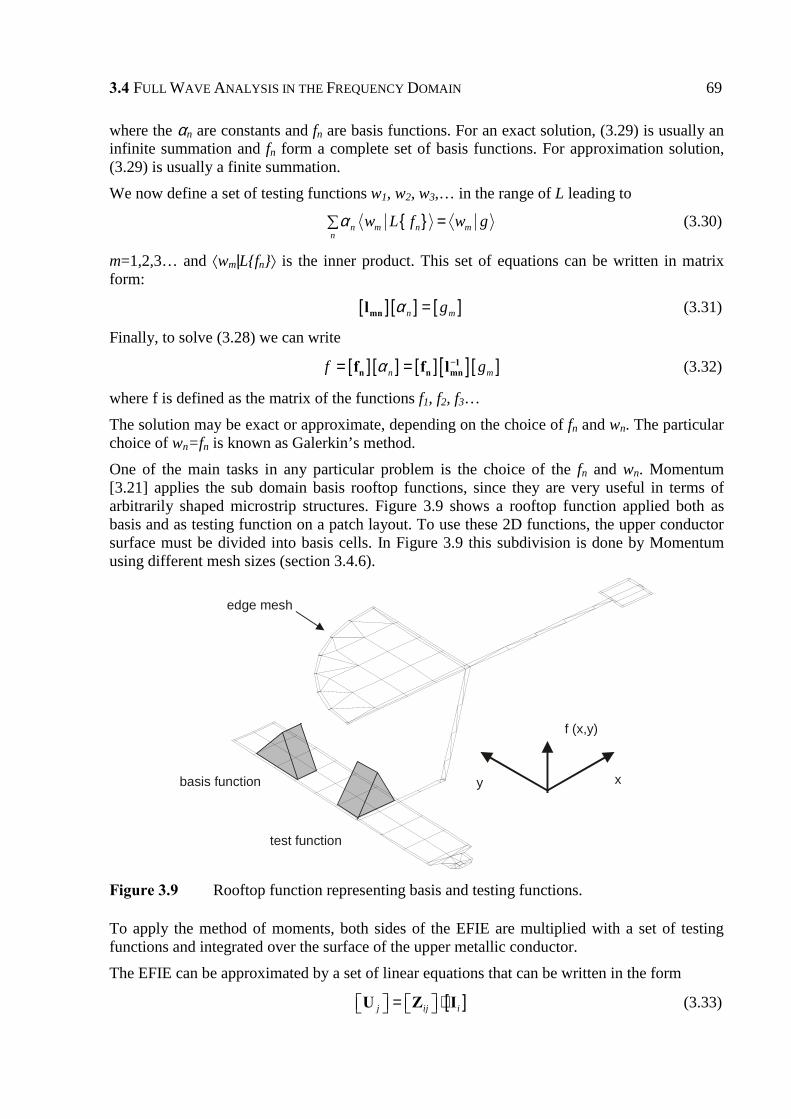
3.4 FULL WAVE ANALYSIS IN THE FREQUENCY DOMAIN 69
where the αn are constants and fn are basis functions. For an exact solution, (3.29) is usually an infinite summation and fn form a complete set of basis functions. For approximation solution, (3.29) is usually a finite summation.
We now define a set of testing functions w1, w2, w3,… in the range of L leading to
n m n mn
w L f w gα = (3.30)
m=1,2,3… and wm|Lfn is the inner product. This set of equations can be written in matrix form:
[ ][ ] [ ]n mgα =mnl (3.31)
Finally, to solve (3.28) we can write
[ ][ ] [ ] [ ] [ ]n mf gα −= = 1n n mnf f l (3.32)
where f is defined as the matrix of the functions f1, f2, f3…
The solution may be exact or approximate, depending on the choice of fn and wn. The particular choice of wn=fn is known as Galerkin’s method.
One of the main tasks in any particular problem is the choice of the fn and wn. Momentum [3.21] applies the sub domain basis rooftop functions, since they are very useful in terms of arbitrarily shaped microstrip structures. Figure 3.9 shows a rooftop function applied both as basis and as testing function on a patch layout. To use these 2D functions, the upper conductor surface must be divided into basis cells. In Figure 3.9 this subdivision is done by Momentum using different mesh sizes (section 3.4.6).
f (x,y)
xybasis function
test function
edge mesh
Figure 3.9 Rooftop function representing basis and testing functions.
To apply the method of moments, both sides of the EFIE are multiplied with a set of testing functions and integrated over the surface of the upper metallic conductor.
The EFIE can be approximated by a set of linear equations that can be written in the form
[ ]j ij i= ⋅ U Z I (3.33)
70 3 CIRCUIT AND DEVICE MODELS AND THEIR IMPLEMENTATION FOR AIA DESIGN
where U represent the known excitation vector (field sources), Z is the so-called generalized impedance matrix that represents the reaction integrals based on the Green’s functions (imped-ance functions), and I is the surface current distribution to be determined. For a single layer microstrip structure (3.33) can be written as following, where the suffixes are defined according to (3.26)
= ⋅
o,x xx xy x
0,y yx yy y
U Z Z IU Z Z I
(3.34)
3.4.4 Calculation of the Impedance Matrix The reaction integral equation (compare with [3.22]) is solved in the spectral domain. This transformation shows the advantage that, instead of a four-dimensional integral, only a two-dimensional surface integral must be solved. Since the scalar Green’s functions show singulari-ties due to the dielectric, the contour of integration must be selected carefully. To save compu-tation time, the symmetry properties of the matrix are exploited.
To derive the surface current distribution I, the matrix equation (3.34) is solved applying itera-tive methods, e.g. the method of conjugated residues.
Based on the current distribution, the port impedance, the scattering, and antenna parameters can be calculated.
3.4.5 Calculation of the Input Impedance Before calculating the input impedance, the field quantities must be transformed to network quantities. Considering uniplanar feeding, the port voltage is calculated from the excitation field (3.22), where the integration path is the infinitesimal gap. The port current is derived from a surface integration over the current distribution of the excited basis cell
=
dAJdsE
Z (3.35)
3.4.6 Implementation of the Full-Wave Analysis in “Momentum” There are some opportunities to influence the numerical solver within momentum [3.21]. By choosing the metallization as discretization layer, we know that the EFIE are used. Simulation expense can be influenced by choosing the “mesh” representing the size of the basis and testing functions in 3.4.3. By increasing the number of these cells, simulation time and accuracy can be improved since the modeling of the surface currents is improved.
As can be seen, the choice of the excitation is a crucial parameter for the calculation of the cur-rent density (section 3.4.3) as well as the input impedance (section 3.4.5). Different port types are available in “momentum”:
• Transmission line ports (TL)
• Point feed ports (PF) Using TL ports models a typical microstrip port, where the ground metallization is used as ref-erence. This TL configuration does not represent the uniplanar port we use in this work. The connection between the transistor and the microstrip line is realized in flip-chip technology (ap-pendix). Considering network quantities, the port voltages are defined between two ports on the

3.5 COMPARISON OF CIRCUIT AND FIELD SIMULATION 71
upper conductor surface. This can be taken into consideration by using the PF ports. The valid-ity of this assumption is proved with measurements.
Together with the HP Momentum software, the DCS desktop allows direct graphical input of the planar microstrip geometry. Additionally, the layout can be automatically generated from lumped element models.
Another interesting feature of the Momentum software is that the total amplitude of the surface current distribution derived from (3.34) can be visualized quantitative (Figure 3.10). This in-formation can be used to understand the behavior of the circuit, e.g. to find the optimal place to connect bias lines.
current densitylowmediumhigh
Figure 3.10 Surface current distribution of the AIA.
The excitation vectors are derived from the reduced S-parameters in chapter 2. The results con-firm our assumption that the gate is the frequency determining part of the microstrip structure. The other lines make the right impedance available for the drain and source terminals of the transistor. The skin effect results in higher current densities at the line edges. This can be taken into consideration using the “edge-mesh” function where the dimensions of the basis and test-ing functions are reduced at the line edges (Figure 3.9).
3.5 Comparison of Circuit and Field Simulation After the presentation of the behavioral and physical models for both the transistor and the mi-crostrip lines, the properties of these models are evaluated in this section. This is realized in two steps. In a first step, microstrip patches are simulated with both methods, and the results for return loss are compared with measurements.
In a second step, an AIA is designed using both models. Different ways to combine behavioral and physical models as well as linear and nonlinear oscillator theories are discussed and the simulation results are combined with measurements. Due to the usage of linear theory, only the oscillation frequencies of the AIAs are compared. Finally, the results are discussed regarding the accuracy and execution times.
3.5.1 Microstrip Patch Simulation Two patches are selected to examine the simulation accuracy. Patch (a) in Figure 3.11 is the lengthened gate resonator of the realized AIA and patch (b) in Figure 3.11 is a modified version of the low-Q resonator (see chapter 2 for dimensions). For these examinations, the interface is not realized in microstrip (in contrast to the patch used within the AIA). It is realized via a microstrip-coplanar transition designed according to [3.23], to ease the measurements with a VNA. For realization, alumina substrate is used (see appendix for specifications).

72 3 CIRCUIT AND DEVICE MODELS AND THEIR IMPLEMENTATION FOR AIA DESIGN
a b
1 mm
Figure 3.11 Two different patches to examine the simulation accuracy.
20 GHz20 GHz FrequencyFrequency 30 GHz30 GHz
0.75 0.75
mag
(S)
11
mag
(S)
11
1.0 1.0
full wave simulationcircuit simulationmeasurement
Figure 3.12 Comparison of simulated and measured input reflection coefficient different patches.
From Figure 3.12 it can be seen that the simulation results are nearly identical, if low radiation patches (low losses) are simulated. If a broad lossy patch is simulated, the full-wave approach describes the antenna properties in a better way regarding the measurements since circuit simu-lation does not predict radiation. Since we have desired radiation, the preferred simulation method for the AIA design is the full-wave analysis.
3.5.2 AIA Simulation There are different ways to combine the modeling approaches with the different oscillator theo-ries. Figure 3.13 shows possible combinations of the modeling methods with the oscillator theo-ries. Regarding the AIA, four different combinations of the behavioral and physical modeling methods applied for the microstrip structure and the transistor are theoretically possible. These combinations can be applied both for linear and nonlinear oscillator theories.
MicrostripBehavioralModel
MicrostripPhysicalModel
TransistorBehavioralModel
TransistorPhysicalModel
linear and nonlinear modellinglinear modelling only
I
II
III
IV
Figure 3.13 Possible combinations of modeling methods with different oscillator theories.

3.5 COMPARISON OF CIRCUIT AND FIELD SIMULATION 73
Recalling linear oscillator theory, it is obvious that the large-signal modeling of the transistor has no influence on the modeling accuracy. The accuracy can only be influenced by using be-havioral or physical microstrip modeling. On the other hand, nonlinear oscillator theory makes only sense with large-signal modeling of the transistor. Therefore, the following combinations are examined as presented in [3.24]:
• Linear oscillator theory combined with behavioral modeling of both the microstrip structure and the transistor.
• Linear oscillator theory combined with physical modeling of the microstrip structure and behavioral modeling of the transistor.
• Nonlinear oscillator theory combined with behavioral modeling of the microstrip struc-ture and physical modeling of the transistor.
• Nonlinear oscillator theory combined with physical modeling of both the microstrip structure and the transistor.
To compare small-signal and large-signal results, the HBT (section 3.1.3.2) was used biased at Uce = 3 V, Ib = 0,6 mA.
370 µm
Base
Collector
Emitter
Bias Network
3.5 µm Gold Metallization
Silicon Subsrate
1 mm
Figure 3.14 Simulated AIA layout.
The simulated AIA layout is depicted in Figure 3.14. The radiating approximately half-wave length long base (gate) resonator is the dominating structure surrounded by the two emitter (source) lines replacing vias. The collector (drain) is loaded with a non-resonant patch.

74 3 CIRCUIT AND DEVICE MODELS AND THEIR IMPLEMENTATION FOR AIA DESIGN
3.5.3 Results After fabrication (see Appendix), multiple AIAs are measured. The simulation results and the measured frequencies are shown in Table 3.1 for silicon and Table 3.2 for alumina substrates:
Simulation no. Simulation type Simulation result Measurement Relative error
(I) Linear, behavioral 23.6 GHz
(II) Linear, physical 23.6 GHz 0.04%
(III) Non-linear, behavioral 24.0 GHz
(IV) Non-linear, physical 24.0 GHz
23.61 GHz
1.63%
Table 3.1 Simulation and measurement results for an AIA on silicon substrate using dif-ferent methods.
Simulation no. Simulation type Simulation result Measurement Relative error
(I) Linear, behavioral 23.0 GHz 2.34%
(II) Linear, physical 23.6 GHz 0.21%
(III) Non-linear, behavioral 23.6 GHz 0.21%
(IV) Non-linear, physical 24.0 GHz
23.55 GHz
1.88%
Table 3.2 Simulation and measurement results for an AIA on alumina substrate using different methods.
3.5.3.1 Accuracy
Table 3.1 and Table 3.2 show that the error applying the behavioral model with simple linear theory for the AIA has a maximum error of 2.34%. Refining the structure model with full-wave analysis leads to a maximum error of 0.21%. Nonlinear theory combined with behavioral and physical models of the microstrip structure leads to maximum errors of 1.63% and 1.88%, re-spectively. Regarding the maximum errors, it can be seen that linear oscillator analysis com-bined with full-wave analysis of the passive circuit (method II) gives the best results predicting the oscillation frequency of AIA either on silicon or alumina substrate.
The oscillation frequency can be predicted using nonlinear and linear oscillator theories. This behavior was expected regarding the considerations in chapter 2. The effect, that the results from the linear theory are slightly more exact can be explained regarding the transistor model. For small-signal measurements, the exact measured S-parameters are used, representing also the flip-chip interconnection. For nonlinear oscillator theory, a large-signal model of the transis-tor is used, that is more general and a source of small errors due to the number of different pa-rameters involved.
The neglect of losses and coupling gives the divergence regarding simulation method (I). This becomes more obvious in simulation method (III), where the passive structure is also modeled at the higher harmonics. The increasing losses give greater divergences (compare with 3.5.1).
The additional feature of large-signal modeling, namely the power prediction, is of very re-stricted use since only a share of the generated RF-power is radiated into space. It depends fur-

3.6 CALCULATION OF THE ANTENNA PARAMETERS 75
ther on the application how much radiated power can be used because some power is radiated co-polar and some cross polar.
Simulation accuracy depends on many parameters. Even using rigorous modeling algorithms, it is very hard to achieve better simulation accuracy than that achieved in this work, since many parameter influence the realized AIA that cannot be modeled:
• Substrate: Finite substrate dimensions; variation in thickness, εr, losses, and metalliza-tion.
• Transistor parameters: Varying device characteristics
3.5.3.2 Execution Time
Regarding the execution times, it must be differentiated between the time needed to derive the circuit and device models and the time needed for the simulation. Large-signal modeling of the transistor takes a very long time since extensive large-signal measurements are needed to obtain an adequate device model. Small-signal modeling requires only S-parameter measurements of the transistor that are included in the large-signal measurements.
The derivation of the circuit models and the execution times for the simulation can be neglected compared to the derivation of the transistor model and the time needed for the graphical input of the circuit structure.
3.5.4 Conclusion Regarding Table 3.1 and Table 3.2 and having in mind the different execution times, it is obvi-ous that the preferred design method in this work is based on linear theory combined with full wave analysis of the microstrip structure. This method combines the advantages of high simula-tion accuracy together with short execution times. For this reason, all designs used in this work are based on this method.
3.6 Calculation of the Antenna Parameters After calculation of the current distribution in the spectral domain (section 3.4), the radiation properties of the AIA are derived. Below, quantities are described that are of interest since they can be measured directly.
3.6.1 Radiation Pattern The radiation pattern represents the relative radiated power versus azimuth and elevation. It is derived from the far-field and can be calculated for the single AIA as well as the AIA array.
3.6.1.1 Single AIA
The electric field strength at the observer point (r,θ,ϕ) in the far-field of a microstrip patch is
⋅
+−+=
ϕ
θ
ϕθϕθϕϕ
πeee
Er
yx
yx
rjk
EEEE
rek
jo
~cossin~sincos
~sin~cos0
20 (3.36)
with ( )yx kk ,~~~ JGE ⋅= and kx = sinθ cosϕ, k y= k0 sinθ sinϕ, k 0= 2πf/c
76 3 CIRCUIT AND DEVICE MODELS AND THEIR IMPLEMENTATION FOR AIA DESIGN
3.6.1.2 AIA Array
For many applications, a high-gain, narrow pencil beam is required. Since beam-width is in-versely proportional to antenna size, more than one antenna is required to sharpen the radiation beam. An array of antennas working simultaneously can focus the reception or transmission of energy in a direction, which increases the useful range of a system.
Given that individual AIA free-running frequencies and power outputs are nearly identical and the entire array is locked to a common frequency, the radiation pattern will behave according to
Etotal = Element pattern × Array factor (3.37) with
( )0
,4
jk reElement pattern fr
θ φπ
−
= (3.38)
( )( )01 cos
1
z zN
j i k di
iArray factor I e θ β− +
== (3.39)
The same far-field approximations apply for the phase and magnitude terms of the total electric field. Assuming identical elements also allows separating the element pattern from the array factor
( ) ( )( )
( )( )
001 cos
1,
4z z
jk r Nj i k d
total ii
eE f I er
Element pattern Array Factor
θ βθ ϕπ
−− +
==
= − (3.40)
The antenna element normally serves as a resonator, radiator, and DC bias pad. Biasing and device integration disturb the radiation patterns and disrupt polarization purity of the antenna. In addition, individual device parameters vary, and tolerance errors during fabrication cause AIA array sources to operate at different frequencies. Although the frequencies may be close enough and coupling between elements may be high enough to synchronize the entire array to a single frequency, the output power and combining efficiency suffers. After the determination of the radiation pattern, the bandwidth, directivity, and the side lobe behavior of the antenna are calculated.
3.6.2 Polarization An important parameter to describe the radiation properties of the antenna is the polarization. It describes the behavior of the electric field vector. The far-field vector can be divided in two orthogonal components. For a patch, the polarization is linear. The direction of the vector for maximum radiation is called the main transmitting direction (co-polarization). The cross-polarization vector Emax differs from the co-polarization vector Emin by 90° and represents the direction with the lowest radiated power
cos sinsin cos ϕ
α αα α
− = ⋅
θmax
min
EEEE
where ( )2 2
2arctan ϕ
ϕ
αℜ
=−
*θ
θ
E E
E E (3.41)
A measure for the polarization is the cross-polarization directivity for linear polarization
linXPD = max
min
EE
(3.42)
3.6 CALCULATION OF THE ANTENNA PARAMETERS 77
3.6.3 Radiated Power The radiated power of the antenna is determined by integrating (3.36) over the complete half-space above the upper conductor surface. This can be written in terms of Poynting’s vector Tr
( ) ( )2 / 2
2 2
00 0 / 2lim lim sin sinr r
P r d r d dπ π δ π
δϕ θ θ π δθ θ θ θ ϕ
−
→∞ →= = = +
= ℜ + ℜ r rT T (3.43)
As no antenna terminal is available, it is impossible to specify radiated power and gain. There-fore, new parameters have been established. For transmitters, effective isotropic radiated power (EIRP or ERP) is specified in the peak direction:
24ERP rπ= rT (3.44)
where Tr is the Poynting’s vector and r is the distance between the AIA and the receiving an-tenna. Assuming we receive the power Pr with a receiving antenna with the effective area Aeff, Poynting’s vector can be described as:
r
eff
PA
=rT (3.45)
If the physical antenna aperture is used instead of the effective, a desired underestimation of the Poynting’s vector takes place.
3.6.4 Gain The antenna gain is defined as the ratio of the intensity to the radiation intensity that would be received if the power accepted by the antenna would be radiated isotropically in a given direc-tion [3.25]. The reference antenna is a spherical source so that the gain can be expressed as
( ) 24 , ,r
i
r rGP
π θ ϕℜ= T (3.46)
where Tr is Poynting’s vector defined as
22
02r rFZ
ϕ+= θE E
T e (3.47)
The reference power is the active power at the input terminal of the antenna. The reference power is defined as
ℜ=
i
iii Z
UUP
*
(3.48)
where Ui and Zi are the voltage and reference impedance at the input terminal.
The gain depends on the orientation between the antenna and the observer point. Maximum gain is achieved if the observer point is located in the main transmitting direction.
Gain in AIAs is difficult to quantify because the measured co-polarized and cross-polarized field components must be integrated over all angels. In addition, it is difficult to calibrate power in AIAs. An approximation for the antenna gain can be found using Kraus’ approximation given in [3.25]

78 3 CIRCUIT AND DEVICE MODELS AND THEIR IMPLEMENTATION FOR AIA DESIGN
32400GΕ Η
≈Ω Ω
(3.49)
with ΩE and ΩH are the half–power beamwidths in the E-and H-plane, respectively, in degrees.
3.6.5 DC to RF Conversion Efficiency The DC to RF conversion efficiency is, probably, the most important parameter in AIAs. It de-pends on the solid-state device used, and it explains the evolution from active patch antennas from diodes to transistors. If the RF power conversion is very high but goes to the antenna’s cross-polarization component, it is wasted. In this sense, it is more important to speak of the RF power converted to the co-polarization component for AIAs.
The actual oscillator conversion is more difficult to ascertain since the antenna is physically inseparable from the device. This is why the efficiency for AIAs ηDC-RF is defined as the ratio between the radiated power and the DC input power
DCDC
rRFDC IU
P⋅
=−η (3.50)
Using the ERP, the isotropic conversion efficiency can be defined
DC ERPDC DC
ERPU I
η − = (3.51)
3.6.6 Visualization With the commercial Method of Moments solver momentum, some antenna parameters are calculated by the software and must not be evaluated analytically. Based on the current distribu-tion, the far-field can be calculated and visualized. The far-field data is shown in chapter 4 and compared with the measured radiation patterns.
3.6.7 Estimation of the Main Radiating Patch Regarding the radiation pattern of an AIA, it is interesting to know what part of the microstrip structure dominates the radiation behavior. From our theoretical considerations, we assume that the gate resonator is dominating but we do not know the radiation is influenced by the remain-ing structure.
To examine this influence we make a theoretical experiment. We switch the excitation sources at each port on and off and observe changes of the radiation behavior. This experiment cannot be applied in practice since the frequency determining and radiation properties of the microstrip lines cannot be separated.
After verifying the influence of the single lines, it can be seen that the gate resonator dominates the radiation behavior as expected. If the radiation of the gate resonator is neglected, the total radiated power decreases by the factor 20.
It is important to know how radiation happens to simulate mutual coupling. Because of our ex-periment we know that it is sufficient to consider the gate resonator if coupling is examined. We admit only a small error neglecting the influence of the remaining microstrip structure on the coupling. This simplifies the coupling modeling considerably.

4 EXPERIMENTAL VALIDATION OF THE AIA DESIGNS
After designing different antenna types, the results are validated with measurements in this chapter. All relevant oscillator and antenna properties are characterized. The depiction starts with the free running AIA followed by the voltage controlled and the injection-locked AIA. The last section deals with the characterization of a complete AIA array consisting of four AIAs.
4.1 Measuring AIAs Measurement methods for AIAs are not as standardized as those of microwave circuits or pas-sive antennas. The main reason is that there is no well-defined output port as in circuits, and on the other hand the antenna exhibits gain larger than that dictated by its effective area, due to the active device. Therefore, it is important to use the correct figures of merit as defined in chapter 3 and to describe first the measurement methods.
4.1.1 Frequency and Output Power It is difficult to measure the absolute radiated output power without having a well-defined out-put port. However, it is very often sufficient to measure the relative power with respect to changes in the operating conditions.
Consequently, the following equipment is needed to measure the frequency and output power:
1. DC power supplies (one or two depending what transistor is used and how it is biased)
2. Receiving antenna (standard gain horn if the absolute power is required)
3. Spectrum analyzer
4. Power meter (to calibrate the spectrum analyzer and to measure the power)
The distance between the AIA and the receiving antenna must be chosen large enough so that the AIA is not loaded by the receiving antenna and small enough to allow the detection of the signal. If the power level is determined, the receiving antenna must be operated in the far-field of the AIA (section 4.1.3).
4.1.2 Q-Factor and Phase Noise
4.1.2.1 Methods
The simplest, easiest, and perhaps oldest method for phase noise analysis of sources is the di-rect spectrum technique. Here, the device under test is input to a spectrum analyzer tuned to the carrier frequency, directly measuring the power spectral density of the oscillator in terms of L(f). The second technique for making short-term stability measurements on sources is commonly called the “time domain” technique. The DUT and the reference are down converted with a mixer to a low IF frequency. Then a high resolution counter repeatedly counts the IF signal, with the time between each measurement held constant. This allows several calculations of the

80 4 EXPERIMENTAL VALIDATION OF THE AIA DESIGNS
fractional time difference over the time period use. A special variance over these differences can then be calculated.
The third method of phase noise measurement is commonly called the phase detector method. This method provides good sensitivity over the entire frequency range; it can be used to meas-ure high quality standards or free running oscillators. The heart of this method is the phase detector. Two sources at the same frequency and in phase quadrature are input to a double-balanced mixer used as a phase detector. The mixer sum frequency is filtered off and the differ-ence frequency is 0 Hz with an average voltage output of 0 V. Riding on this dc signal are ac voltage fluctuations proportional to the combined phase noise of the two sources.
The fourth method of phase noise measurement on sources is called the frequency discriminator method. In this method, the frequency fluctuations of the source are translated to baseband volt-age fluctuations that can then be measured by a baseband analyzer.
Since the phase noise of AIAs is high compared to crystal or highly synchronized oscillators and the phase noise is only of interest for frequencies > 10 kHz, the first “Direct spectrum” method was used to characterize the AIAs.
4.1.2.2 Direct Spectrum Method
Direct spectrum analysis is useful for measuring sources with relatively high phase noise, but there are some restrictions using the direct spectrum method: A spectrum analyzer cannot dis-tinguish amplitude modulation from phase or frequency modulation. The definition of L(f) is the power measured in one phase modulation sideband divided by the total carrier power. In order for a valid number for L(f), the sideband power measured must be the phase modulation sidebands only. Thus, for accurate phase noise measurements using the direct spectrum method, the source’s AM noise must be << PM noise. In measuring random noise, the 3 dB bandwidth and shape can also limit the resolution of discrete noise. Even with a narrow bandwidth, the shape factor of the spectrum analyzer will limit the resolution of close-in noise, or any noise close to a high level spur. To improve measurement sensitivity an alternate direct spectrum technique can be used which consists of a selective receiver and a low phase noise local oscilla-tor.
4.1.2.3 Application of the Direct Spectrum Method
To measure the phase noise directly in a one hertz bandwidth, the “MKNOISE” function of the spectrum analyzer can be used. With this option, the rms noise level at the marker position is normalized to a one hertz bandwidth compensating the following errors:
• Irregular shape of resolution-bandwidth filters
• Log amplifiers
• Difference between the rms values of the noise floor envelope (which is a narrowband re-sponse described by Rayleigh’s distribution function) and the true rms value of the noise floor (which is a broadband response)
Using the “DELTA” mode, the offset frequency can be inserted directly, and the marker read-out shows the wanted L(f).
4.1.2.4 Deriving the Q-Factor from the Phase Noise Measurements
After measuring the phase noise density to carrier ration L(f) with the direct spectrum method, the Q-factor can be derived according to chapter 2:

4.1 MEASURING AIAS 81
( )
2
01 18 ( )m
fFkTQ QC L f f L f
= ⋅ ⋅
(4.1)
4.1.3 Radiation Behavior Typically, antenna pattern measurements require large separation to be in the far-field where the phase front across the main lobe is nearly spherical and the field distribution is independent of the distance from the antenna. If the maximal linear dimension of the antenna is D, the con-dition for far-field operation is approximately:
λ
22DR ≥ (4.2)
where R is the transmitter receiver distance and D > λ must be satisfied. AIAs can be tested using conventional antenna measurement equipment but require additional DC bias lines to operate the active device. Additionally, they are inherently good Doppler Sen-sors. Therefore, any disturbance or quick movements by the rotator are translated into fre-quency shifts of the AIA. Although it is a great quality for automatic door openers and car alarms, it adds more uncertainties during a pattern test.
Figure 4.1 Measurement setup for radiation pattern measurements.
Figure 4.1 shows a photograph of the used measurement setup. The distance between the AIA and the receiving antenna is 50 cm. The receiving antenna is mounted on an arm that can be turned by 180° and fixed in steps of 10° so that the movement of the arm does not affect the measurements. The power variation is measured with a spectrum analyzer and recorded in de-pendence of the angle. Co- and cross-polarization is measured by orienting the AIA according to the polarization of the receiving antenna.
For radiation pattern measurements, it is important to define a system of spherical coordinates. Figure 4.2 shows how the coordinate system is defined with respect to the AIA. All radiation
82 4 EXPERIMENTAL VALIDATION OF THE AIA DESIGNS
pattern measurements are based on this definition. The definition of the planes of the radiation pattern assuming linearly polarized radiation is shown in Table 4.1:
co cross
E-plane (φ = 0, 180°) Etheta Ephi
H-plane (φ = 90, -90°) Ephi Etheta
Table 4.1 Definition of the polarization.
z
x
y
θ
φ
E-planeH-plane
Figure 4.2 Coordinate system for the antenna measurements.
4.2 Single Free-Running AIA Since the free running AIA is the starting point for the other AIA types and applications, the characterization is very important. Based on the results, it can be decided if possible theoretical improvements can be implemented and what applications can be realized with these AIAs.
The characterization starts with the measurement of the oscillation frequency and the radiated power depending on the DC power. Regarding sensor applications, the self-mixing behavior is of special interest. Exploiting this behavior, Doppler measurements can be carried out effec-tively. Phase noise is another interesting feature of AIAs. It is investigated for the AIA with the λ/2 long gate resonator and the phase noise improved λ long gate resonator (compare chapter 2). The characterization of the radiation behavior concludes this section. Two different transis-tor types are used for the characterization. If it is not indicated explicitly, the HEMT based AIA is used, otherwise, the HBT based AIA finds application.
For all measurements, the AIAs are mounted on a gold header. The substrate is glued with a conductive paste on the header and the bias lines are connected to the pins of the header with bond wires. The usage of these headers allows better handling of the front-ends. Figure 4.3 shows a photograph of a free running AIA on a gold header.

4.2 SINGLE FREE-RUNNING AIA 83
1 mm
Figure 4.3 Free running AIA mounted on a gold header.
4.2.1 Bias Effects on Output Frequency and Power The operation frequency of the AIA was measured with a spectrum analyzer depending on the DC operation conditions and the measurements were compared with simulations.
23,0
23,2
23,4
23,6
23,8
24,0
0 1 2 3U ds [V]
I d [m
A]
0
4
8
12
16
20
freq
uenc
y [G
Hz]
Figure 4.4 Output frequency and drain current as a function of drain bias voltage for the HEMT based AIA.
Regarding Figure 4.4 it can be seen that the AIA shows the expected DC dependency of the oscillation frequency. Oscillation starts up at 23.1 GHz for low transistor voltages and oscilla-tion frequency increases up to 24 GHz for the simulated bias conditions. Comparing the simu-lated frequencies with the measured frequencies it can be seen that the oscillation frequency can be predicted very exactly using linearized oscillator theory (0.2%) and nonlinear oscillator the-ory (1.9%) (Table 4.2):
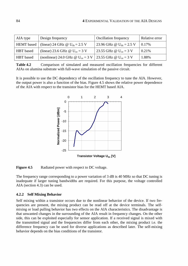
84 4 EXPERIMENTAL VALIDATION OF THE AIA DESIGNS
AIA type Design frequency Oscillation frequency Relative error
HEMT based (linear) 24 GHz @ Uds = 2.5 V 23.96 GHz @ Uds = 2.5 V 0.17%
HBT based (linear) 23.6 GHz @ Uce = 3 V 23.55 GHz @ Uce = 3 V 0.21%
HBT based (nonlinear) 24.0 GHz @ Uce = 3 V 23.55 GHz @ Uce = 3 V 1.88%
Table 4.2 Comparison of simulated and measured oscillation frequencies for different AIAs on alumina substrate with full-wave simulation of the passive circuit.
It is possible to use the DC dependency of the oscillation frequency to tune the AIA. However, the output power is also a function of the bias. Figure 4.5 shows the relative power dependence of the AIA with respect to the transistor bias for the HEMT based AIA.
-25
-20
-15
-10
-5
00 1 2 3 4
Transistor Voltage Uds [V]
Nor
mal
ized
Pow
er [d
Bm
]
Figure 4.5 Radiated power with respect to DC voltage.
The frequency range corresponding to a power variation of 3 dB is 40 MHz so that DC tuning is inadequate if larger tuning bandwidths are required. For this purpose, the voltage controlled AIA (section 4.3) can be used.
4.2.2 Self Mixing Behavior Self mixing within a transistor occurs due to the nonlinear behavior of the device. If two fre-quencies are present, the mixing product can be read off at the device terminals. The self-mixing or load pulling behavior has two effects on the AIA characteristics. The disadvantage is that unwanted changes in the surrounding of the AIA result in frequency changes. On the other side, this can be exploited especially for sensor application. If a received signal is mixed with the transmitted signal and the frequencies differ from each other, the mixing product i.e. the difference frequency can be used for diverse applications as described later. The self-mixing behavior depends on the bias conditions of the transistor.

4.2 SINGLE FREE-RUNNING AIA 85
300
250
200
150
100
50
0
U [m
V]IF
0.5 1.0 1.5 2.0U [V]ds
Figure 4.6 Voltage level of the intermediate frequency due to the self-mixing process within the transistor with respect to the drain voltage of the transistor.
To verify the self-mixing behavior, a slowly oscillating reflector was placed in the far-field of the AIA. Because of the Doppler effect, the reflected signal shows a different frequency than the transmitted signal. The amplitude of the intermediate frequency (IF) due to the self-mixing process measured at the drain terminal of the transistor is shown in Figure 4.6 with respect to the transistor drain voltage. For a transistor drain source voltage of 1 V, maximum self-mixing occurs. However, the oscillation frequency for maximum self-mixing is 23.4 GHz (compare Figure 4.4) that is 600 MHz lower than the design frequency since the AIA was designed for a transistor drain source voltage of 2.5 V. For many applications, the IF at 2.5 V is sufficient to achieve a satisfactory Doppler signal. To achieve a larger Doppler signal, the AIA must be de-signed to oscillate at 1 V with the desired frequency.
4.2.3 Q-Factor and Phase Noise From our theoretical considerations, the loaded Q-factor was assumed to be QL = 9.17. There-fore, we are expecting a high phase noise of the free-running AIA. To prove this assumption, the spectrum of the free running AIA given in Figure 4.7 is needed.
500 kHz / DIV
CF = 24 GHz, RBW = VBW = 1 kHz, SPAN = 5 MHz
0
-20
-40
-60
Nor
mal
ized
Pow
er [d
Bm]
-80
Figure 4.7 Spectrum of the free-running AIA.

86 4 EXPERIMENTAL VALIDATION OF THE AIA DESIGNS
Using the direct spectrum method, the phase noise can be derived from the spectrum and num-bers are given in Table 4.3:
Offset frequency Phase noise L(f)
100 kHz -30 dBc/Hz
1 MHz -60 dBc/Hz
Table 4.3 Phase noise of the free running AIA.
The phase noise shows the expected behavior. Due to this low Q, the spectrum is very broad compared to a synchronized source, and it becomes obvious that the free running AIA cannot be used for rigorous sensor and communication applications.
As presented in chapter 2, the phase noise of the free running AIA can be influenced by chang-ing the gate resonator geometry, while the oscillation frequency remains constant. To improve the phase noise, a λ/2 lengthened gate resonator with a higher Q-factor is used. Based on this resonator, an AIA is developed using the linear oscillator theory (Figure 4.8).
4 mm
Figure 4.8 Picture of the AIA with the lengthened (phase noise improved) gate resonator.
The measured spectrum is shown in Figure 4.9 with both peaks normalized. Oscillation fre-quency is 24 GHz, giving a design accuracy compared to measurements of 0.1%. It can be seen that the phase noise using the lengthened gate resonator (black) is improved compared to the original design (gray). Numbers for the phase noise are given in Table 4.4. The phase noise of the AIA with the lengthened gate resonator is -35 dBc/Hz (@ 100 kHz offset) compared to -30 dBc/Hz of the original AIA. This is consistent with the expected 6 dB phase noise im-provement from Eq. (4.1) since the QL is improved by the factor 2 (chapter 2).
The third discussed approach in chapter 2, the gate resonator consisting of a broad, low-impedance patch, has a lower Q compared to the resonators discussed here. An AIA based on this resonator was also characterized. The design accuracy was also proven with this approach (simulation accuracy compare to measurements 0.2%). Since its phase noise and radiation be-havior did not show any advantages compared to the AIAs presented here, no results are given here.

4.2 SINGLE FREE-RUNNING AIA 87
CF = 24 GHz, RBW = VBW = 1 kHz, SPAN = 5 MHz
500 kHz / DIV
0
-20
-40
-60Nor
mal
ized
Pow
er [d
Bm]
-80
Figure 4.9 Measured spectrum if the AIA with improved phase noise properties.
Offset frequency Phase noise L(f)
100 kHz -35 dBc/Hz
1 MHz -63 dBc/Hz
Table 4.4 Phase noise of the free running AIA w/ improved Q resonator.
4.2.4 Radiation Behavior Regarding possible applications, it is important to know the radiation characteristic of the free running AIA. The direction of the main radiation beam must be known to orientate the AIA in the right angle with respect to the observed object (for sensor applications) or the receiver (for communication applications). The pattern was measured as described above and the measure-ments are compared with the expected pattern derived from the calculation of the antenna char-acteristics.
-300
30
60
90 -30 -200 -40
co measuredco simulatedcross measuredcross simulated
theta [°]
relative power [dB]
E-plane
Figure 4.10 Radiation pattern of the free-running AIA (E-plane).

88 4 EXPERIMENTAL VALIDATION OF THE AIA DESIGNS
-300
30
60
90 -30 -200 -40
co measuredco simulatedcross measuredcross simulated
theta [°]
relative power [dB]
H-plane
Figure 4.11 Radiation pattern of the free-running AIA (H-plane).
It is worth mentioning that in Figure 4.10 and Figure 4.11, the agreement between measure-ments and simulations is quite satisfactory. The co-polarization patterns in both planes show symmetrical behavior. The cross-polarization is only 10 dB lower than the co-polarization. This is caused by the bias lines around the actual antenna structure. We assume that the radial stubs (Figure 4.3) radiate in the orthogonal direction compared to the antenna. This assumption is confirmed with a simulation. Though it cannot be proven with measurements, it is possible to simulate the AIA structure without all bias lines. The simulation result is shown in Figure 4.12. The co-polarization remains unchanged whereas the cross-polarization nearly disappears.
Since the radial stubs are very close to the substrate edge, the calculation error of the cross-polarization is larger compared to the prediction of the radiation from the actual antenna (i.e. co-polarization). The substrate edges are also responsible for the high radiation for large |θ|. This is due to the radiation caused by substrate waves.
-30-3000
3030
6060
9090 -30 -30 -20 -20 00 -40-40
cross w/ stubscross w/o stubs
co w/ stubsco w/o stubs
theta[°]theta [°]
relative power [dB]relative power [dB]
H-plane
Figure 4.12 Simulations of the AIA structure w/ and w/o bias lines in the H-plane.
The port excitation vectors for the calculation of the far-field are derived from the adapted lin-ear simulation results. Though this approach is relatively simple, the conformity between the simulation and the measurements is impressive.

4.2 SINGLE FREE-RUNNING AIA 89
The lengthened gate resonator to improve the phase noise also influences the radiation behav-ior. Figure 4.13 and Figure 4.14 show the radiation pattern of the phase noise improved AIA with respect to the original AIA in the E- and H-plane, respectively. In both planes, the unde-sired cross-polarization is raised about 10 dB. In addition, the uniform co-polarization pattern of the original AIA shows multiple lobes in the E-plane and H-plane due to the lengthened gate resonator. To sum up, the radiation behavior of the phase noise improved AIA is deteriorating compared to the original AIA. Regarding possible applications, the selection of the preferred AIA depends if phase noise or radiation properties are more important.
Though the original AIA has poorer phase noise, it is used for the injection locking and cou-pling due to its more uniform radiation pattern.
-300
30
60
90 -30 -200 -40
co short resonatorco long resonatorcross short resonatorcross long resonator
theta [°]
relative power [dB]
E-plane
Figure 4.13 Radiation pattern of phase noise improved AIA compared to the free-running AIA (E-plane).
-300
30
60
90 -30 -200 -40
co short resonatorco long resonatorcross short resonatorcross long resonator
theta [°]
relative power [dB]
H-plane
Figure 4.14 Radiation pattern of phase noise improved AIA compared to the free-running AIA (H-plane).
4.2.5 Effective Radiated Power, Antenna Gain, and Conversion Efficiency Following the theory described in chapter 3, the effective radiated power and the isotropic con-version efficiency of the original AIA (w/o lengthened gate resonator) can be determined (Table 4.5). The receiving antenna is the input of a waveguide. Using the physical size results in a desired underestimation of the Poynting’s vector.

90 4 EXPERIMENTAL VALIDATION OF THE AIA DESIGNS
Measured power in main radiation direction -29.1 dBm @ 24 GHz
Distance between AIA and receiving antenna 30 cm (satisfying Eq. (4.2))
Dimension of the receiving antenna 10.7×4.3 mm2
Poynting’s vector 2.67 µW/cm2
ERP 30.2 mW, 14.8 dBm
DC power (Figure 4.4) 60 mW
Isotropic conversion efficiency ηDC-ERP 50.3%
Table 4.5 Measure effective radiated power and isotropic conversion efficiency.
The antenna gain is derived from the far-field measurements. The half-power beamwidths can be derived from Figure 4.10 and Figure 4.11 and are given in Table 4.6.
ΩE = ΩH 100°
Gain 3.24 dB
Table 4.6 Half-power beamwidths and gain of the AIA.
Regarding the results presented in this section, it can be seen that the free running AIA can be used as the starting point for the following verifications, but also as a front end for multiple applications. The bias dependence of the frequency can be used for frequency tuning and load-pulling effects are usable for Doppler applications. The radiation behavior with the large half-power beamwidth is another promising feature for applications making the AIA insensitive to tilt angles.
4.3 Frequency Tunable AIA Using a varactor diode, the AIA can be tuned [4.1]. By adjusting the diode voltage, different oscillation frequencies can be achieved. According to chapter 2, three different approaches were realized (Figure 4.15). Beginning with the direct approach (Figure 4.15 a) all three approaches are discussed in this section. Since the inductive approach (Figure 4.15 c) shows the best re-sults, it is considered in detail.
ba c
Figure 4.15 Pictures of the voltage controlled AIAs.

4.3 FREQUENCY TUNABLE AIA 91
4.3.1 Tuning Range The first VCAIA characterized is the directly coupled VCAIA. As predicted with simulations, the tuning range is nearly 3 GHz (12.5%, Figure 4.16). The deviation between the simulation and the measurement is due to the loading effect of the diode to the transistor that cannot be modeled with small-signal simulations. This effect is getting stronger with increasing cut-off voltage of the diode. The loading effect resulting from the diode is also responsible for the strong output power variation (29 dB). This variation can only be reduced if the feedback of the diode is reduced by means of indirect coupling.
21
22,5
24
25,5
27
0 5 10 15 20U_Varactor [-V]
f[GHz
]
-25
-16
-7
2
11
rel.p
ower
[dB]
Figure 4.16 Oscillation frequency (simulated and measured) and radiated power with re-spect to varactor voltage of the directly coupled VCAIA.
23
23,6
24,2
0 5 10 15 20U_Varactor [-V]
f[G
Hz]
-9
0
9
rel.
pow
er[d
B]
f_simf_mespower
a b
Figure 4.17 Oscillation frequency (simulated and measured) and radiated power with re-spect to varactor voltage of the capacitive (a) and inductive (b) coupled VCAIAs.
Indirect coupling is realized in two ways with the diode arranged at the gate resonator. A cou-pling gap is used to realize capacitively coupling (Figure 4.15 b) and a thin high inductive line is used for inductively coupling (Figure 4.15 c). As predicted with the simulation, the capacitive

92 4 EXPERIMENTAL VALIDATION OF THE AIA DESIGNS
approach shows multi-moding effects (Figure 4.17 a). Due to the length of the gate resonator together with the coupling gap, two slightly different modes depending on the diode voltage can exist. This assumption is confirmed regarding the radiated power from the VCAIA. For a diode voltage [0; -5 V], the first radiating mode exists. For a diode voltage [-5 V; -10 V], the VCAIA shows chaotic like behavior resulting in a decrease of the radiation by 10 dB. For diode volt-ages [-10 V; -20 V], the VCAIA radiates in the second mode with nearly constant power that is around 10 dB larger than the power from the first mode and 20 dB larger than the power radi-ated during the mode switching.
Inductively coupling (Figure 4.17 b) shows ideal behavior. Though the tuning range is smaller than using direct coupling (4.2% compared to 12.5%, Figure 4.16), the frequency is propor-tional to the diode voltage. Moreover, the power remains constant over the diode voltage [-5 V; -15 V] if the drain source voltage is UDS = 2.5 V. Using the inductively coupled AIA, the tuning range is 4.2% and the relative power variation is 0.3 dB.
-15
-10
-5
0
5
10
0 5 10 15 20
U_Varactor [-V]
rel.
pow
er[d
B]
U =1.5VDS
U =2.0VDS
U =2.5VDS
a b
Figure 4.18 Radiated power versus transistor voltage for the indirect coupled VCAIAs.
Regarding the radiated power behavior versus the transistor voltage (Figure 4.18), it can be seen that the transistor voltage must be selected carefully. The inductively coupled VCAIA (Figure 4.18 b) shows the desired power flatness only for relatively large drain source voltages (2.5 V). For small transistor voltages, the diode influences the transistor significantly. This observation is in accordance with the self-mixing behavior of the transistor, which is also caused by load pulling effects.
This effect cannot be observed regarding the capacitive approach (Figure 4.18 a). The coupling between the diode and the transistor is too weak in this case to enable any feedback. Therefore, the power behavior is independent from the transistor voltage.

4.3 FREQUENCY TUNABLE AIA 93
4.3.2 Phase Noise
500 kHz / DIV
CF = 24 GHz, RBW = VBW = 1 kHz, SPAN = 5 MHz
0
-20
-40
-60
Nor
mal
ized
Pow
er [d
Bm]
-80
Figure 4.19 Spectrum of the inductively coupled AIA (black) compared to the free running AIA (gray).
Offset frequency Phase noise L(f)
100 kHz -33 dBc/Hz
1 MHz -63 dBc/Hz
Table 4.7 Phase noise of the inductively coupled VCAIA.
The phase noise behavior of the inductively coupled voltage controlled AIA is 3 dB better compared to the free running AIA (Figure 4.19). Table 4.7 shows numbers of the phase noise measured with the direct spectrum method. The improvement compared to the free running AIA is due to the longer gate resonator. We observed this behavior already examining gate resonators with different shapes in section 4.2.3. Applying Eq. (4.1), we know that the Q-factor of the gate resonator with the inductive line is raised by the factor of 1.41 compared to the free running AIA.
4.3.3 Radiation Behavior To simulate the radiation behavior, we calculated the microstrip structure of the inductive cou-pled VCAIA. Though we are able to consider the transistor inserting the calculated port volt-ages, the diode cannot be considered. Therefore, we have a larger simulation error compared to the single free running AIA. Especially regarding the cross-polarization (Figure 4.20), it is hard to predict the behavior since this is dominated by the bias lines. We assume that the neglect of the influence of the diode is responsible for the simulation error of 20 dB in the cross polariza-tion of the E-plane.
The co-polarization can be predicted with sufficient accuracy. The dip in the co-polarization in the E-plane for θ = 0° (Figure 4.20) is due to the near one wavelength long gate resonator (com-pare also Figure 4.13).

94 4 EXPERIMENTAL VALIDATION OF THE AIA DESIGNS
-300
30
60
90 -30 -200 -40
co measuredco simulatedcross measuredcross simulated
theta [°]
relative power [dB]
E-plane
-300
30
60
90 -30 -200 -40
co measuredco simulatedcross measuredcross simulated
theta [°]
relative power [dB]
H-plane
Figure 4.20 Radiation pattern of the inductive approach for different varactor voltages.
After characterization, it can be seen that the inductive coupled VCAIA meets the requirements better than the other VCAIAs. The linear tuning range comes together with the linear output power if the right transistor voltage is chosen. Regarding the radiation pattern, the long gate resonator causes a tilt of the main radiation direction as well as a dip for θ = 0°.
4.4 Injection-Locked AIA
gold header
koax linecoming throughthe header
inner conductorsoldered on the substrate
AIA
Figure 4.21 Picture of the injection-locked AIA.

4.4 INJECTION-LOCKED AIA 95
Injection locking can be used either for synchronization or for phase noise reduction. We use injection locking to verify how far the phase noise of the AIA can be reduced. In our approach, the AIA layout remains unchanged since the injection signal is coupled through a gap into the gate resonator. The injection-locked AIA is shown in Figure 4.21. The dimensions are in accor-dance with chapter 2. We feed the AIA by means of a semi-rigid coax line that is led through the gold header. The inner conductor of this line is soldered on a coupling line that is supplied on the substrate. The injection signal is made available from a synthesizer.
4.4.1 Locking Range
0
2
4
6
8
-10 -5 0
Injection power [dBm]
Tuni
ngba
ndw
idth
[MH
z]
Figure 4.22 Locking range with respect to injection power.
Figure 4.22 shows the tuning bandwidths for an injection-locked AIA with respect to the injec-tion signal strength. The plot shows the increase of locking bandwidth with an increase in injec-tion-locking signal. The injection power is measured at the input of the coax line. The locking gain versus locking bandwidth graph is especially important for AIAs because they are easily affected by the environment. In power combining applications, the locking gain and bandwidth determine how much power is required to keep the distributed sources synchronized to a master source.
With the injection-locking theory presented in chapter 2 and the Q-factor of the gate resonator (Q = 130), we can calculate the ratio of the injection power with respect to the AIA power. For a tuning bandwidth of 7 MHz, the difference between the injection and the AIA power is 28 dB. To increase the tuning bandwidth, the coupling between the inner conductor and the AIA must be improved.

96 4 EXPERIMENTAL VALIDATION OF THE AIA DESIGNS
4.4.2 Phase Noise
-90
-80
-70
-60
-50
-40
-30
-20
-10
0
-4 -2 0 2 4
rel. frequency [MHz]
Phas
eno
ise
[dB
c/H
z]@
100k
Hz
Figure 4.23 Phase noise with respect to tuning frequency for –5 dBm injection power.
The phase noise behavior of the injection-locked AIA depends on the tuning bandwidth as well as on the phase noise of the injection source. Figure 4.23 shows the phase noise of the injection-locked AIA for an injection power of –5 dBm. According to chapter 2, the phase of for the in-jection-locked AIA is equal to the phase noise of the injection source. For frequencies outside the bandwidth, the phase noise is that of the free running AIA. Table 4.8 shows numbers of the phase noise for the injection-locked AIA within the locking range. The phase noise values out-side the locking range can be found in section 4.2.3.
Offset frequency Phase noise L(f)
100 kHz -82 dBc/Hz
1 MHz -94 dBc/Hz
Table 4.8 Phase noise of the injection-locked AIA.
500 kHz / DIV
CF = 24 GHz, RBW = VBW = 1 kHz, SPAN = 5 MHz
0
-20
-40
-60
Nor
mal
ized
Pow
er [d
Bm]
-80
Figure 4.24 Spectra of the injection-locked AIA compared with the free-running AIA.
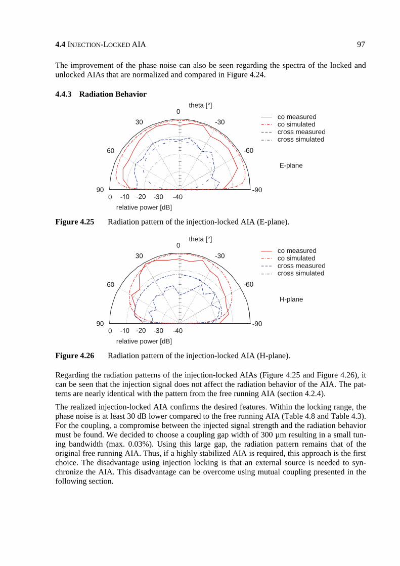
4.4 INJECTION-LOCKED AIA 97
The improvement of the phase noise can also be seen regarding the spectra of the locked and unlocked AIAs that are normalized and compared in Figure 4.24.
4.4.3 Radiation Behavior
-300
30
60
90 -30 -200 -40
co measuredco simulatedcross measuredcross simulated
theta [°]
relative power [dB]
E-plane
Figure 4.25 Radiation pattern of the injection-locked AIA (E-plane).
-300
30
60
90 -30 -200 -40
co measuredco simulatedcross measuredcross simulated
theta [°]
relative power [dB]
H-plane
Figure 4.26 Radiation pattern of the injection-locked AIA (H-plane).
Regarding the radiation patterns of the injection-locked AIAs (Figure 4.25 and Figure 4.26), it can be seen that the injection signal does not affect the radiation behavior of the AIA. The pat-terns are nearly identical with the pattern from the free running AIA (section 4.2.4).
The realized injection-locked AIA confirms the desired features. Within the locking range, the phase noise is at least 30 dB lower compared to the free running AIA (Table 4.8 and Table 4.3). For the coupling, a compromise between the injected signal strength and the radiation behavior must be found. We decided to choose a coupling gap width of 300 µm resulting in a small tun-ing bandwidth (max. 0.03%). Using this large gap, the radiation pattern remains that of the original free running AIA. Thus, if a highly stabilized AIA is required, this approach is the first choice. The disadvantage using injection locking is that an external source is needed to syn-chronize the AIA. This disadvantage can be overcome using mutual coupling presented in the following section.
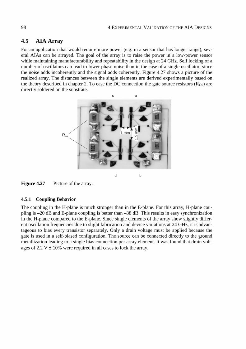
98 4 EXPERIMENTAL VALIDATION OF THE AIA DESIGNS
4.5 AIA Array For an application that would require more power (e.g. in a sensor that has longer range), sev-eral AIAs can be arrayed. The goal of the array is to raise the power in a low-power sensor while maintaining manufacturability and repeatability in the design at 24 GHz. Self locking of a number of oscillators can lead to lower phase noise than in the case of a single oscillator, since the noise adds incoherently and the signal adds coherently. Figure 4.27 shows a picture of the realized array. The distances between the single elements are derived experimentally based on the theory described in chapter 2. To ease the DC connection the gate source resistors (RGS) are directly soldered on the substrate.
1 mm1.
5 m
mRGS
d b
ac
Figure 4.27 Picture of the array.
4.5.1 Coupling Behavior The coupling in the H-plane is much stronger than in the E-plane. For this array, H-plane cou-pling is –20 dB and E-plane coupling is better than –38 dB. This results in easy synchronization in the H-plane compared to the E-plane. Since single elements of the array show slightly differ-ent oscillation frequencies due to slight fabrication and device variations at 24 GHz, it is advan-tageous to bias every transistor separately. Only a drain voltage must be applied because the gate is used in a self-biased configuration. The source can be connected directly to the ground metallization leading to a single bias connection per array element. It was found that drain volt-ages of 2.2 V ± 10% were required in all cases to lock the array.

4.5 AIA ARRAY 99
4.5.2 Phase Noise
500 kHz / DIV
CF = 24 GHz, RBW = VBW = 1 kHz, SPAN = 5 MHz
0
-20
-40
-60
Nor
mal
ized
Pow
er [d
Bm]
-80
Figure 4.28 Spectra of the single free running AIA (gray) and the synchronized array (black).
The resulting spectrum if all elements of the array are coupled is shown in Figure 4.28. The spectrum of a single AIA (gray) is compared with the spectrum of the complete locked array (black) where both peaks are normalized. If all AIAs are locked, the phase noise is -37 dBm / Hz (@ 100 kHz offset, Table 4.9) and the radiated output power density measured in the main lobe by means of a field probe at a distance of 20 cm is 10 dB higher compared to a single AIA. Ideally, the power density should be n2 that of the single element where n is the number of locked AIAs, giving an achieved combining efficiency greater than 63% for the ar-ray in Figure 4.27. According to the theory presented in chapter 2, the phase noise should im-prove by 1/n. The measured phase noise improvement of 7 dB proves therefore the in-phase coupling.
100 kHz -37 dBc/Hz
1 MHz -65 dBc/Hz
Table 4.9 Phase noise of AIA array.
4.5.3 Radiation Behavior
AIA array
DC probes
Figure 4.29 Far-field measurement setup for the AIA array with DC probes.
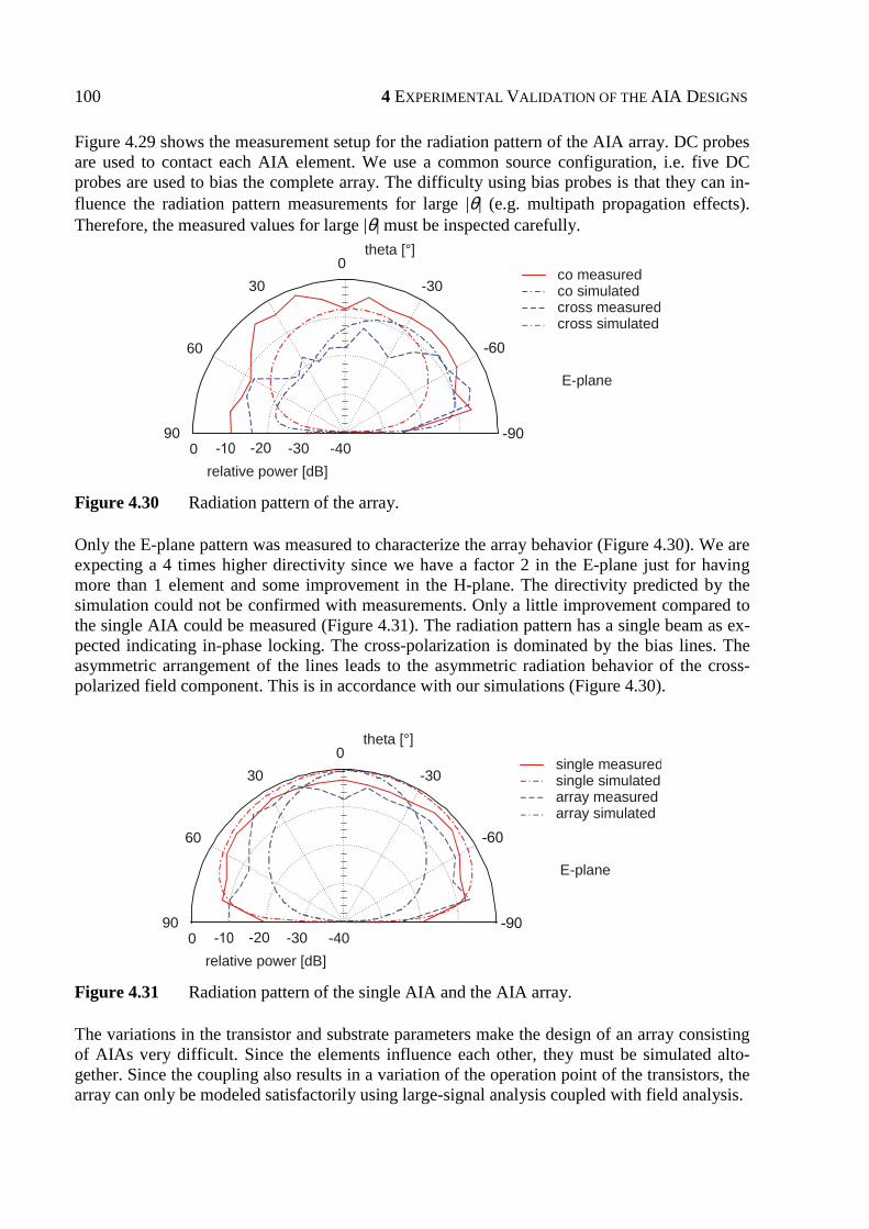
100 4 EXPERIMENTAL VALIDATION OF THE AIA DESIGNS
Figure 4.29 shows the measurement setup for the radiation pattern of the AIA array. DC probes are used to contact each AIA element. We use a common source configuration, i.e. five DC probes are used to bias the complete array. The difficulty using bias probes is that they can in-fluence the radiation pattern measurements for large |θ| (e.g. multipath propagation effects). Therefore, the measured values for large |θ| must be inspected carefully.
-300
30
60
90 -30 -200 -40
co measuredco simulatedcross measuredcross simulated
theta [°]
relative power [dB]
E-plane
Figure 4.30 Radiation pattern of the array.
Only the E-plane pattern was measured to characterize the array behavior (Figure 4.30). We are expecting a 4 times higher directivity since we have a factor 2 in the E-plane just for having more than 1 element and some improvement in the H-plane. The directivity predicted by the simulation could not be confirmed with measurements. Only a little improvement compared to the single AIA could be measured (Figure 4.31). The radiation pattern has a single beam as ex-pected indicating in-phase locking. The cross-polarization is dominated by the bias lines. The asymmetric arrangement of the lines leads to the asymmetric radiation behavior of the cross-polarized field component. This is in accordance with our simulations (Figure 4.30).
-300
30
60
90 -30 -200 -40
single measuredsingle simulatedarray measuredarray simulated
theta [°]
relative power [dB]
E-plane
Figure 4.31 Radiation pattern of the single AIA and the AIA array.
The variations in the transistor and substrate parameters make the design of an array consisting of AIAs very difficult. Since the elements influence each other, they must be simulated alto-gether. Since the coupling also results in a variation of the operation point of the transistors, the array can only be modeled satisfactorily using large-signal analysis coupled with field analysis.

4.5 AIA ARRAY 101
To summarize, coupling of AIAs can be used to improve the total radiated power by 10 dB as well as the phase noise by 7 dB. With the configuration presented here, the radiation behavior does not change.

5 SENSOR AND COMMUNICATION APPLICATIONS
After validation of the designs presented in chapter 2, it was shown in chapter 4 that AIAs show features that make them very attractive for sensor and communication applications. Features such as easy and cheap production, as well as excellent reproducibility makes them first-choice front-ends for many applications. In this work, two applications are considered in detail.
Regarding the AIA properties, not all applications can be realized with AIAs. Due to the rela-tively high phase noise, frequency and amplitude modulation is not recommended, however, spread spectrum modulation can be used [5.1].
The self-mixing properties of the free running AIA can be exploited for Doppler applications. Figure 5.1 shows an AIA based Doppler sensor that is mounted on the rear bumper of a car. The operation principle of this sensor can be described as follows: The AIA transmits a CW signal that is reflected by the road surface. Due to the Doppler effect, the reflected signal is frequency shifted proportional to the velocity over ground. Within the transistor, the reflected and fre-quency shifted signal is mixed with the transmitted signal leading to an intermediate frequency that is proportional to the speed over ground.
Rearbumper
Dopplersensor
Figure 5.1 Doppler sensor mounted on a car.
This Doppler sensor is developed in this work. In addition, a crash sensor based on this sensor is developed that allows for the first time predictive crash analysis. Regarding communication applications, the first imaging RFID system is developed and is presented here.
In this chapter, the RFID system and the crash sensor are presented in detail including the op-eration principle, the realization, and the results from operation.

5.1 RFID SYSTEM 103
5.1 RFID System The first imaging RFID system based on AIAs is presented. The block diagram of the RFID system is shown in Figure 5.2 [5.2]. The system can be divided into two parts: The active trans-mitter and the imaging receiver.
=1
500 kHz
Code
Mux1/32
15.625 kHz
5x5 DetectorarrayLens
24GHz1
25
500kHz
90°
AGCID-Tag
Figure 5.2 Block diagram of the RFID system.
The modulated signal is transmitted by the so-called tag and is received by a 5×5 array of rec-tennas. After analog signal processing, the signal is digitized, processed in a digital signal proc-essor (DSP), and displayed on a computer screen. Since the tag is realized in a relative simple way, most of the system intelligence is found in the receiver. This has the advantage that the tags can be realized cost effective, which is important because multiple tags are used in a sys-tem and only one receiver is needed. The details of this system are discussed in the following sections.
5.1.1 The Active Transmitter “Tag” The tag can be divided in three parts that are explained in detail in the following subsections:
• The RF front-end
• The code generator
• The power supply
5.1.1.1 The RF Front-End
The free running AIA is used as the RF front-end in this system. The ISM band at 24.125 GHz ± 125 MHz gives the boundary conditions for the frequency range.
The transistor gate is biased in a self-biasing configuration with a 10 kΩ resistor between the gate and source terminals. The drain is used as the modulation input. On-off keying is applied to modulate the AIA with the modulation code. Since the output frequency depends on the drain voltage, the finite width of the signal flanks causes a frequency ramp. This must be considered designing the code generator.

104 5 SENSOR AND COMMUNICATION APPLICATIONS
5.1.1.2 The Code Generator
With regard to simple realization, maximal length pseudo noise (PN) sequences are used which employ good correlation properties. This identification code modulates via BPSK the 24 GHz AIA by means of a sub carrier technique. The codes are called maximal length sequences and are applied in this work with a length of 31 bits. They are generated using a quartz oscillator that is connected to CMOS shift registers. The feedback loops of these shift registers define the code. The quartz oscillator of the code generator determines the modulation frequency (500 kHz) and the code frequency (15.625 kHz). The length of the 31 bit code is 1.98 ms. Since it is important to have short flanks, a 1 kΩ resistor is applied parallel to the AIA.
5.1.1.3 The Power Supply
The AIA and the code generator must be supplied with power. We use a 3 V lithium cell that is placed under the circuit board of the tag. Though the lifetime of the battery limits the lifetime of the complete tag, large read ranges can be achieved with this approach.
1 cm
AIA
quartz
code generator
battery
Figure 5.3 The active tag.
The complete assembled tag is shown in Figure 5.3. The AIA is mounted on a gold header on top of the circuit board together with the quartz and the code generator. The battery can be found under the circuit board.
Using the codes transmitted by the tag, we are able to identify things or persons. To localize things in addition, we need the localization functionality of the receiver.

5.1 RFID SYSTEM 105
5.1.2 The Imaging Receiver The receiver is responsible for both the identifying and localizing properties of the system. The receiver can be divided into different parts:
• The lens for quasi-optical beamforming
• The detector array consisting of 25 detectors
• The analog signal processing
• The digital signal processing
5.1.2.1 The Lens for Quasi-Optical Beamforming
Quasi optical properties can be exploited if the diameter of the lens is much larger than the wavelength of the electromagnetic wave. With a wavelength of 1.25 cm @ 24 GHz and a lens diameter of 17.3 cm, this condition is satisfied.
Regarding the lens shape, monofocal lenses are limited to very small scan angles. Therefore, we designed a bifocal lens from HD-PE (εr = 2.3) with a focus of 22.7 cm allowing for larger scan angles. The calculation of the lens surface shape is based on Snellius’ law on the guideline to obtain a planar phase front of the waves going through the lens. The parameters of the lens are given in 5.1.4.
Figure 5.4 shows that the received power level and the beam forming properties are almost con-stant for scan-angles up to ±13°. The -3 dB far field beam angle is smaller than 2.7°.
-40
-35
-30
-25
-20
-15
-10
-5
0
5
-25 -20 -15 -10 -5 0 5 10 15 20 25
Angle [°]
Nor
mal
ized
Inte
nsity
[dB
] Scan-angle 0°
Scan-angle 6.5°
Scan-angle 13°
Figure 5.4 Radiation patterns of lens-focused rectennas.
5.1.2.2 The Detector
Every detector is realized as rectifying antenna (rectenna). Here, the rectenna is a planar dipole antenna with a Schottky diode in between the monopoles. Figure 5.2 shows a picture of such a planar rectenna. The length of the dipole is approximate λg/2, where λg is the guided wave-length of the microstrip line. The length of the dipole must be adapted so that the dipole imped-ance is matched conjugate complex to the Schottky impedance. In this application, the Schottky

106 5 SENSOR AND COMMUNICATION APPLICATIONS
diode (small cube in the middle of Figure 5.5) represents a nonlinear resistor that demodulates the RF signal.
To select the optimal dimensions of the rectenna, different dipoles were characterized. The measurements showed that the length of the dipoles must be shortened by 10% to take the ef-fects of the small substrate dimensions into consideration. The DC connections are realized as a low pass filter structure with radial stubs to decouple the RF signal. The 3 dB bandwidth of the detector is 750 MHz.
PlanarDipole
Schottky-Diode
1 mm
Figure 5.5 Rectenna at 24 GHz.
Besides depending on the geometry, the sensitivity of the detector can be influenced by biasing the Schottky diode. Though the diode noise depends also on the diode current, the signal-to-noise-ratio of the rectenna is improved. The optimal diode current was experimentally deter-mined to be 50 µA.
5.1.2.3 The Detector Array
The detector array is responsible for the localizing feature of the system. In our system, we aligned the detectors with respect to the lens so that the -3 dB points of the antenna patterns of two adjacent detectors coincide. As can be seen in Figure 5.4, in this case the cross-talk due to side lobes is below -15 dB. To achieve adequate resolution, 25 rectennas are arranged in a 5×5 array.
Rectenna ongold header
3 cm
Figure 5.6 The detector array.
Figure 5.6 shows a photograph of the complete detector array (17×17 cm2). In contrast to exist-ing imaging systems, a two-dimensional approach is used, so that no expensive mechanical scanning is necessary.

5.1 RFID SYSTEM 107
Each detector comes on a header so that it can be easily replaced. The circuit board between the detectors is covered with absorber to avoid multipath reception. On a second layer behind the detectors, the power supplies and the pre-amplifiers can be found.
5.1.2.4 The Analog Signal Processing
For the RFID system, the analog signal processing is a rigorous task, since the power level of the signal is very low, and direct detection of the RF signals is used.
After the direct detection, the 500 kHz IF (Intermediate Frequency) signal is pre-amplified with a high-speed operational amplifier having a gain of 100. The noise of the pre-amplifier can be neglected compared to the diode noise.
Following the amplification, signal quality can be improved further with band pass filtering. Considering the spectra of the desired code, it can be represented by the si(x)2 function around 500 kHz. Theoretically, the spectrum is indefinite. By neglecting the spectra outside the main lobe of the si function only 10% of the signal energy is lost but the signal-to-noise-ratio is im-proved significantly. The band pass is realized as a Bessel-Thompson-Filter of the fourth order.
To allow for digitization of the tag signal, the power level of the different detectors must be normalized to a signal swing of 5 V. This is done with an automatic gain control amplifier.
The IF of the direct detected signal is too high to be processed by the A/D converter and the signal processor. Therefore, the signal must be down converted directly into the base band. Since the tag and the receiver are not synchronized, frequency and phase offsets are created due to the mixing. To minimize this disadvantage, complex mixing is applied.
The two phase-shifted signals are digitized in a 10-bit A/D converter, compared, and the signal with the lowest offset is used for the subsequent correlation. The sampling frequency fs of the converter is selected to avoid aliasing and satisfying
xcodes samplesofnumberTf 2== . (5.1)
Here, with Tcode = 1.984 ms, 128 samples and fs = 64.516 kHz are used to sample one code.
5.1.2.5 The Digital Signal Processing
After digitization, the signals can be processed by the DSP TMS 320C240. This processor has a 16-bit fix point architecture with a maximum speed of 20 MIPS. The processor is responsible for the identification task of the system.
To recognize a tag, the received and digitized code is compared with a known code within the DSP. This comparison is done with a correlation in the frequency domain. This is faster than doing a correlation in the time domain. The decision criterion for the correlation is the merit factor that is defined as the ratio between the energy of the main correlation peak to the energy of the cross correlation function.
The DSP code is written in both C and assembler. Figure 5.7 shows the structogram of the DSP code. The purpose of the code is to identify and localize three different tags. The merit factors are transferred to PC via a serial interface.

108 5 SENSOR AND COMMUNICATION APPLICATIONS
Initialization
FFT-Transformation of the original codes
Calculation of the conjugate complex spectra: S1, S2, S3
Loading 128 complex values via ADC
Digitizing AGC voltage level, averaging 20 values: agcvoltage
Switching multiplexer to the next detector
FFT-Transformation of S: SADC
Calculation of KKFspec=Si2 SADC
FFT-Transformation of KKFspec into time-domain
Calculation of the magnitude of the KKF
Calculation of the energy of the KKF: energy
Calculation of the energy of the maximum of the KKF: energymax
i2 = 0..2
Calculation of MF[i2]=energymax/energy
Transmission of the detector number i to the PC
Transmission of agcvoltage to the PC
∞ i = 1..25
K = 0..2 Transmission of MF[k] to the PC
Figure 5.7 Structogram of the DSP code.
5.1.3 Visualization After evaluation of the digitized base band signals, the merit factors are transferred to a PC. All 25 merit factors are displayed on the computer screen. A tag is identified if the merit factor is larger than an experimentally determined threshold. The localization is realized applying a two-dimensional cubic spline interpolation algorithm on the 25 values that can be assigned to one tag. The maximum of the interpolation gives the coordinates of the tag with respect to the scanned area of the receiver. Figure 5.8 represents a screen dump showing the merit factors of the 25 detectors and 2 arrows giving the relative position of the tag. Only one merit factor is larger than the selected threshold, all other values are faded out. The two arrows indicate the position of the detector with the highest merit factor. The tag number is selected in the window. This screen is displayed for every tag.
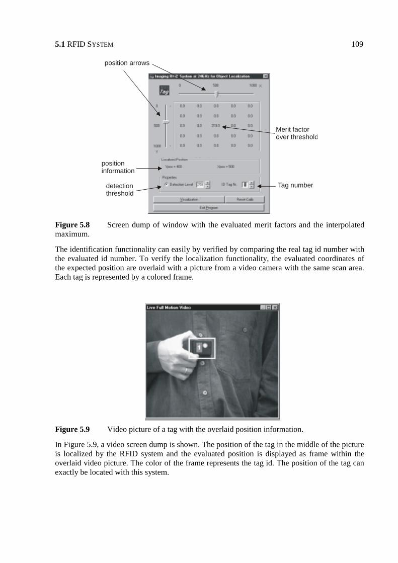
5.1 RFID SYSTEM 109
Tag number
Merit factor over threshold
position arrows
positioninformation
detectionthreshold
Figure 5.8 Screen dump of window with the evaluated merit factors and the interpolated maximum.
The identification functionality can easily by verified by comparing the real tag id number with the evaluated id number. To verify the localization functionality, the evaluated coordinates of the expected position are overlaid with a picture from a video camera with the same scan area. Each tag is represented by a colored frame.
Figure 5.9 Video picture of a tag with the overlaid position information.
In Figure 5.9, a video screen dump is shown. The position of the tag in the middle of the picture is localized by the RFID system and the evaluated position is displayed as frame within the overlaid video picture. The color of the frame represents the tag id. The position of the tag can exactly be located with this system.

110 5 SENSOR AND COMMUNICATION APPLICATIONS
5.1.4 System Data
Operation frequency 24 GHz
Intermediate frequency 500 kHz
Code family Maximum length sequence
Code length 31 bits
Recurrence period 1.984 ms
Number of detectors 25
Area per detector 30 mm × 30 mm
Area of the detector array 17 × 17 cm2
Focal length of the lens 227 mm
Aperture diameter 173 mm
Maximum thickness of the lens 40.2 mm
Diameter of the bifocal area 46 mm
Material of the lens HD-PE (εr = 2.3)
Scan angle 15°
3 dB far field beam width > 3.57°
Local resolution @ 1 m 13 cm
Local resolution @ 1.5 m 19 cm
Local resolution @ 2 m 26 cm
Table 5.1 System data of the realized RFID system.

5.1 RFID SYSTEM 111
5.1.5 Presentation of the System After the system was built and the functionality was proven, it was presented on the 1998 “Electronica” trade fair. The RFID system was combined with a model railway, where the tags were mounted into the rail wagons. The receiver and video camera were fixed two meters above the table to scan the whole railway.
Modeltrain w/ tag
Tag
Monitor with localization/ identification information
Figure 5.10 Model railway with RFID system.
Figure 5.10 shows the model railway. A monitor in the middle of the railway shows the video picture with the overlaid localization information derived by the RFID system. Colored circles show the position of the tags. The tags are localized even if the train is moving fast.
The railway on the trade fair was a perfect eye catcher for the audience. Multiple contacts with visitors showed us possible applications for the system. Moreover, the functionality could be proved due to the one weeklong operation without any failures. The only part that had to be renewed was the battery of the tags.
5.1.6 Possible Improvements The experience from the presentation gave us rise to improve some features of the system. The number of tags can be improved by using a different code family resulting in longer and easy distinguishable codes. These codes should have good correlation properties and should be in-sensitive regarding multipath propagation. If gold codes with a length of 63 bits are used, 65 different tags can be distinguished [5.3]. Longer codes improve the number of distinguishable tags but need more computation time resulting in slower refresh rates.
The lifetime of the tags can be improved either by waking up the tags with a wake-up pulse or by changing the continuous operation into a pulsed operation. By using short pulses and long sleep times, the lifetime of the tags can be enlarged to several years.
For applications in factory buildings, the read range of the system must be enlarged, too. This can be realized by using an antenna-amplifier-balanced mixer configuration instead of the rec-tenna. The evaluation times of the system can be shortened by using a faster DSP and dividing the calculation task between the DSP and a microcontroller [5.4]. The microcontroller observes

112 5 SENSOR AND COMMUNICATION APPLICATIONS
the 25 detectors and selects the detector with the strongest signal so that the DSP has to calcu-late the correlation only for one detector instead of 25 detectors. By selecting the strongest sig-nal, the microcontroller takes over the localization task.
5.2 Crash Sensor Many sensor applications can be realized using AIAs. In this work, the application as a crash sensor is investigated.
Conventional crash sensors measure the deceleration of an object. Regarding modern, heavy cars, important and lifesaving time passes until the deceleration is large enough to activate pas-senger protection devices (e.g. airbags). Especially side crashes need short response times due to the small crumple zone of the side covers.
Our crash sensor can minimize the response time by monitoring the interior of a car door. Two approaches are useful to solve this task. Either the complete interior is monitored resulting in very sensitive sensor, or a shielded sensor is used. The problem using an unshielded sensor is that normal movements (e.g. caused by the door window) affect the performance of the sensor. This can be avoided using a shielded sensor.
5.2.1 Structure of the Crash Sensor The shielded sensor consists of an AIA and a reflector shielded with an expansion bellow. The length of the shielded sensor is restricted by the width of the car door that is only some centime-ters (Figure 5.11).
Brass heatsink
AIA chip Expansion bellow
Reflector1 cm
Figure 5.11 Schematic drawing of the shielded crash sensor.
The AIA is operating in self–mixing mode [5.5] and is mounted on a brass heatsink. In a known distance r0 (typical: r0 = 6 cm) from the sensor chip, a reflector is placed. This reflector can be mechanically connected to the automobile body sheet to be monitored in respect of deforma-tion. Sensor and reflector are capsulated by means of an expansion bellow.
Since the length of the sensor is in the order of some wavelength of the 24 GHz AIA, an AIA based on an IMPATT diode at 61 GHz is used in addition to verify the influence of the wave-length on the sensor behavior.
5.2.1.1 IMPATT Based AIA
The operation frequency of 60 GHz is too high to use transistors as active elements in AIAs. Therefore, we go back on an existing AIA design [5.6], where an IMPATT diode is mounted in the middle of a planar dipole. The complete structure shown in Figure 5.12 is realized on silicon substrate.
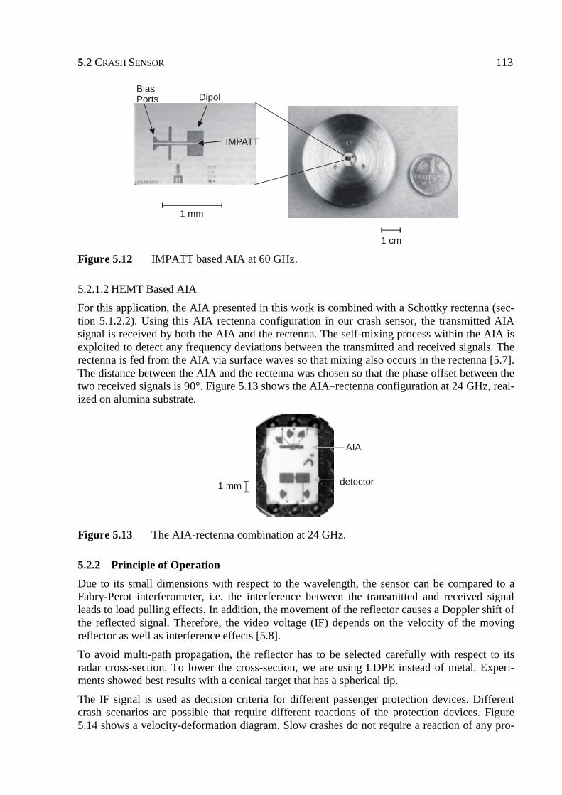
5.2 CRASH SENSOR 113
1 cm
1 mm
Dipol
IMPATT
Bias Ports
Figure 5.12 IMPATT based AIA at 60 GHz.
5.2.1.2 HEMT Based AIA
For this application, the AIA presented in this work is combined with a Schottky rectenna (sec-tion 5.1.2.2). Using this AIA rectenna configuration in our crash sensor, the transmitted AIA signal is received by both the AIA and the rectenna. The self-mixing process within the AIA is exploited to detect any frequency deviations between the transmitted and received signals. The rectenna is fed from the AIA via surface waves so that mixing also occurs in the rectenna [5.7]. The distance between the AIA and the rectenna was chosen so that the phase offset between the two received signals is 90°. Figure 5.13 shows the AIA–rectenna configuration at 24 GHz, real-ized on alumina substrate.
AIA
detector1 mm
Figure 5.13 The AIA-rectenna combination at 24 GHz.
5.2.2 Principle of Operation Due to its small dimensions with respect to the wavelength, the sensor can be compared to a Fabry-Perot interferometer, i.e. the interference between the transmitted and received signal leads to load pulling effects. In addition, the movement of the reflector causes a Doppler shift of the reflected signal. Therefore, the video voltage (IF) depends on the velocity of the moving reflector as well as interference effects [5.8].
To avoid multi-path propagation, the reflector has to be selected carefully with respect to its radar cross-section. To lower the cross-section, we are using LDPE instead of metal. Experi-ments showed best results with a conical target that has a spherical tip.
The IF signal is used as decision criteria for different passenger protection devices. Different crash scenarios are possible that require different reactions of the protection devices. Figure 5.14 shows a velocity-deformation diagram. Slow crashes do not require a reaction of any pro-
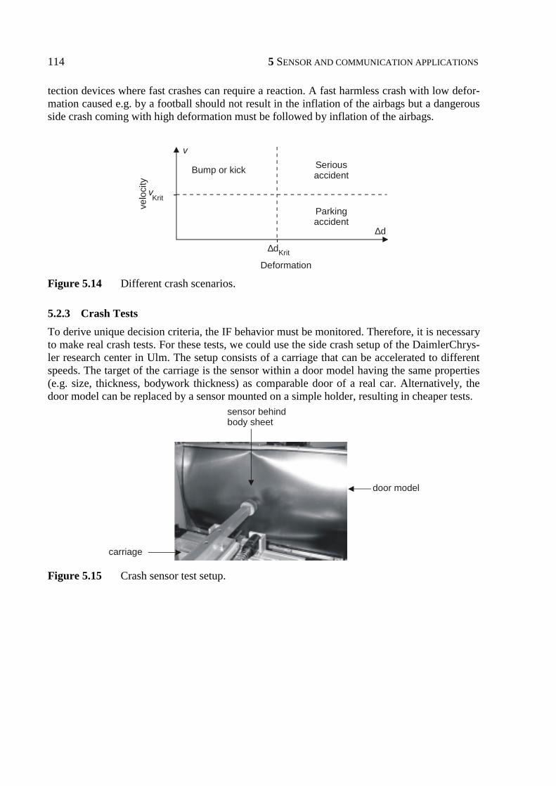
114 5 SENSOR AND COMMUNICATION APPLICATIONS
tection devices where fast crashes can require a reaction. A fast harmless crash with low defor-mation caused e.g. by a football should not result in the inflation of the airbags but a dangerous side crash coming with high deformation must be followed by inflation of the airbags.
∆d
∆d
v
vKrit
Parkingaccident
Seriousaccident
Krit
Bump or kick
Deformation
velo
city
Figure 5.14 Different crash scenarios.
5.2.3 Crash Tests To derive unique decision criteria, the IF behavior must be monitored. Therefore, it is necessary to make real crash tests. For these tests, we could use the side crash setup of the DaimlerChrys-ler research center in Ulm. The setup consists of a carriage that can be accelerated to different speeds. The target of the carriage is the sensor within a door model having the same properties (e.g. size, thickness, bodywork thickness) as comparable door of a real car. Alternatively, the door model can be replaced by a sensor mounted on a simple holder, resulting in cheaper tests.
door model
carriage
sensor behindbody sheet
Figure 5.15 Crash sensor test setup.

5.2 CRASH SENSOR 115
Figure 5.15 shows the setup with the carriage and the door model. Different tests with different speeds and sensors were carried out with the IMPATT based sensor. The video voltage from the AIA was amplified, sampled, and stored. With our digital scope (TDS 220 by Tektronix), we were able to monitor the time 2 ms before and 8 ms after an individually selectable threshold for the video voltage (Figure 5.16).
Figure 5.16 Video voltage versus time for different crash speeds.
The easiest way to decide if the crash was hard or not is to use the sampled signal by counting the zero setting or peak points. However, the level of the peaks and the number of the zero set-ting points differ considerably. Figure 5.17 shows the number of samples, if a threshold of 7.5 V is selected and the samples over this threshold are added, for different fast and slow crashes. The number of samples varies too much (box) to find a suitable criterion.
0
2040
6080
100120
140
0 2 4 6 8Test Number
Sam
ples
fastslow
0
50
100
150
200
0 2 4 6 8Test Number
Sam
ples
fastslow
Figure 5.17 Number of samples above 7.5 V for the video voltage (left side) and below -0.4 V (right side) for the derivative of the video voltage with respect to multiple tests.
-15
-10
-5
0
5
10
0 0,001 0,002 0,003 0,004 0,005 0,006 0,007 0,008 0,009 0,01
Time [Seconds]
Dop
pler
vol
tage
[Vol
t]
fastslow

116 5 SENSOR AND COMMUNICATION APPLICATIONS
Our way to overcome this problem was to use the first derivative of the video voltage. The peaks of the video voltage are no longer rated by their total height but by their gradient. This gives a much better distinguishable signal (Figure 5.18). Applying again a threshold and adding the samples below it, an unequivocal decision criterion is found (Figure 5.17, box). Even reduc-ing the gating time to 4 ms, signals can easily be distinguished.
Figure 5.18 First derivative of the video voltage for different crashes versus time.
Comparable crash test are also carried out with the HEMT based crash sensor and the results show that we can use the same decision criterion for this kind of sensor. The disadvantage using the HEMT based sensor is the lower frequency (i.e. longer wavelength) compared to the IM-PATT based sensor. This results in fewer zero settings regarding the same time period leading to a weaker decision criterion or a longer observation time. However, using the combined AIA rectenna sensor, the number of zero settings can be doubled.
5.2.4 Discussion The usage of an AIA based crash sensor shows many advantages. Compared to a conventional crash sensor that is mounted in the middle of the underbody, the crash sensor in the door detects body sheet deformations much earlier. In addition, the sensor signal can be used to predict the kind of the future crash (pre-crash analysis). Different airbags and restraint mechanisms can be optimally combined to give the passengers the best protection available to minimize their risk to be injured.
-10
-8
-6
-4
-2
0
2
4
0 0,002 0,004 0,006 0,008 0,01
Time [Seconds]
Vide
o vo
ltage
per
sec
ond
[Vol
t/Sec
ond]
fastslow

6 CONCLUSION
The purpose of this work was to develop an understanding and provide design guidelines for active integrated antennas (AIAs) for sensor and communication applications. These antennas represent an attractive choice as state-of-the-art radar front-ends. In contrast to more conven-tional front-ends, the AIA is treated as a single entity. The drawbacks of this approach are that AIAs are difficult to design, and their properties differ from front-ends that are designed to ful-fill a specific task (i.e. highly stabilized transmitters or high directivity antennas). The minimi-zation of these drawbacks while maintaining the advantages of the AIA was the main task of this work. Different AIA concepts were investigated, design procedures for them were estab-lished, prototypes were fabricated and tested, and the AIAs found use for diverse applications, ranging from Doppler sensors to RFID (Radio frequency identification) systems.
AIAs can be realized in multiple ways at different frequencies within the ISM bands. Whereas a number of AIAs have already been demonstrated at frequencies around 2.45 GHz and 5.8 GHz, AIAs presented at frequencies higher than 20 GHz have the disadvantage that the employed two-terminal devices show poor DC-RF efficiency. Transistors have better DC-RF efficiency, and are now commercially available for frequencies above 20 GHz. Therefore, we concentrated on AIAs at the ISM frequency of 24 GHz based on transistors realized in microstrip technology. This technology allows the usage of an “uniplanar” approach, because the complete functional-ity can be integrated on one layer, making the AIA manufacturable and inexpensive.
The design of AIAs is difficult due to the direct interaction between the active device and the antenna. Exact modeling of the complete structure can be done using nonlinear oscillator and electromagnetic theory. This requires the computationally expensive derivation of nonlinear models. Within this work, it was verified that also linear and linearized oscillator theories can be used that lead to the same results. Different theories were introduced consisting of S-parameter representations and narrowband equivalent circuit models.
The first front-end developed in this work was a free-running fixed-frequency AIA. To compare different oscillator theories, the start-up condition was simulated with linear theory, while the steady-state condition was simulated with nonlinear theory. To derive S-parameters for the steady state, large-signal measurements of the transistor were carried out, and it was shown that only |S21| must be reduced by a factor of 40-50% to consider saturation effects. Combining the reduced S-parameters with linearized large signal modeling gave the same oscillation frequency as the small-signal approach of 24 GHz.
When designing AIAs, not only different theories must be considered but also different circuit and device models. Regarding the transistor, a large or a small signal model can be used. The microstrip circuit can be simulated with lumped elements or full-wave analysis. The most rig-orous way to simulate the AIA is to combine nonlinear oscillator theory with a large signal model of the transistor and full-wave analysis of the microstrip circuit. The derivation of these models is very extensive. Therefore, the validity of the simple linear approximations was exam-

118 6 CONCLUSION
ined. Simple small signal models were compared with large signal models, and the results were compared. The average simulation accuracy compared to measurements was 0.21% using small-signal models and 1.63% using large signal models. Both results were satisfactory, so that the linearized approach was adopted due to its efficiency. Additionally, the problems with obtaining good nonlinear device models at these very high frequencies are: non-availability of broadband (100 GHz), active load-pull measurement setup, proper deembedding of 80 nonlin-ear device parameters based on four measured complex numbers, and huge influence of para-sitic reactances. The divergence of 1.4% using the large signal model compared to the small-signal model was due to the very complex large-signal model that was a source of multiple er-rors in contrast to the small-signal model based on measurements.
With the steady state S-parameters, the radiation behavior of the AIA was modeled and meas-ured. The antenna pattern showed the desired behavior with one linear polarized main lobe. This was confirmed with pattern measurements giving an effective radiated power of 14.8 dBm, a half power beamwidth of 100°, and an antenna gain of 3.24 dB. The phase noise of the free running AIA was -30 dBc/Hz @ 100 kHz offset.
This single AIA can be used as a low-cost Doppler-sensor exploiting the self-mixing due to the nonlinearities of the transistor. The amplitude of the intermediate frequency (IF) had its opti-mum for low drain-source voltages, which had to be considered in the AIA design. However, to achieve larger tuning bandwidths than 40 MHz coming with a 3 dB power variation, frequency tunable AIAs had to be used.
A frequency tunable AIA is needed for postproduction tuning and for applications such as FM-CW radars. The frequency-determining element of the AIA is the gate resonator that was made electronically tunable by means of a varactor diode. The coupling of the varactor diode was realized in three different ways. Direct coupling was compared with inductive and capacitive coupling. Direct coupling showed the advantage of a large tuning bandwidth (12.5%), however, the transistor was loaded by the diode resulting in huge output power variations (29 dB). Ca-pacitive coupling showed chaotic-like behavior making this approach not applicable. The inductive approach, on the other hand, combined the advantages of a linear tuning range (4.2%) with power flatness over the tuning range (0.3 dB). The tuning behavior of all three approaches was predicted with linear theory. Due to the lengthened gate resonator, the radiation behavior also changed. The radiation pattern became a 6 dB dip in the E-plane and the phase noise was improved by 3 dB compared to the fixed frequency AIA.
Phase noise is a big issue especially for communication applications. In this work, it was veri-fied how to improve the phase noise by selecting the optimal gate resonator geometry. For this purpose, three different gate resonators were developed for the AIA and their Q-factors were compared. Starting with the resonator from the free-running AIA, it was lengthened by the fac-tor of λ/2 leading to a phase noise improvement of 5 dB. This is in accordance with the ex-pected improvement of 6 dB due to the improved QL by a factor of 2. Alternatively, a low impedance resonator was also investigated. The decreased QL (76% of the original value) of this resonator did not result in any improvement of the AIA properties.
Using a dielectric resonator (DR) coupled to the AIA, the phase noise can also be improved. Two ways are possible to couple a DR to an oscillator. Serial coupling to the gate resonator or parallel coupling between two lines is possible. Regarding serial coupling, the line-DR ar-rangement shows band-stop like behavior around resonance so that oscillation condition is not satisfied for the AIA. Parallel coupling is theoretically possible between every combination of two transistor terminals. Applying linear oscillator theory, it was verified that the DR must be placed between the gate and drain terminals of the transistor to satisfy the oscillation condition. The transmission behavior of this arrangement was characterized. Though the transmission can
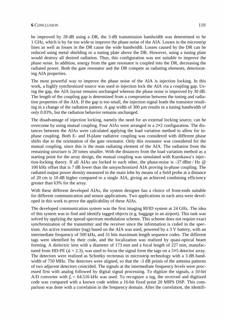
6 CONCLUSION 119
be improved by 28 dB using a DR, the 3 dB transmission bandwidth was determined to be 1 GHz, which is by far too wide to improve the phase noise of the AIA. Losses in the microstrip lines as well as losses in the DR cause the wide bandwidth. Losses caused by the DR can be reduced using metal shielding or a tuning plate above the DR. However, using a tuning plate would destroy all desired radiation. Thus, this configuration was not suitable to improve the phase noise. In addition, energy from the gate resonator is coupled into the DR, decreasing the radiated power. Both the gate resonator and the DR compete as radiating elements, deteriorat-ing AIA properties.
The most powerful way to improve the phase noise of the AIA is injection locking. In this work, a highly synchronized source was used to injection lock the AIA via a coupling gap. Us-ing the gap, the AIA layout remains unchanged whereas the phase noise is improved by 30 dB. The length of the coupling gap is determined from a compromise between the tuning and radia-tion properties of the AIA. If the gap is too small, the injection signal loads the transistor result-ing in a change of the radiation pattern. A gap width of 300 µm results in a tuning bandwidth of only 0.03%, but the radiation behavior remains unchanged.
The disadvantage of injection locking, namely the need for an external locking source, can be overcome by using mutual coupling. Four AIAs were arranged in a 2×2 configuration. The dis-tances between the AIAs were calculated applying the load variation method to allow for in-phase coupling. Both E- and H-plane radiative coupling was considered with different phase shifts due to the orientation of the gate resonator. Only this resonator was considered for the mutual coupling, since this is the main radiating element of the AIA. The radiation from the remaining structure is 20 times smaller. With the distances from the load variation method as a starting point for the array design, the mutual coupling was simulated with Kurokawa’s injec-tion-locking theory. If all AIAs are locked to each other, the phase-noise is -37 dBm / Hz @ 100 kHz offset that is 7 dB lower than the unsynchronized AIA proving in-phase coupling. The radiated output power density measured in the main lobe by means of a field probe at a distance of 20 cm is 10 dB higher compared to a single AIA, giving an achieved combining efficiency greater than 63% for the array.
With these different developed AIAs, the system designer has a choice of front-ends suitable for different communication and sensor applications. Two applications in each area were devel-oped in this work to prove the applicability of these AIAs.
The developed communication system was the first imaging RFID system at 24 GHz. The idea of this system was to find and identify tagged objects (e.g. baggage in an airport). This task was solved by applying the spread spectrum modulation scheme. This scheme does not require exact synchronization of the transmitter and the receiver since the information is coded in the spec-trum. An active transmitter (tag) based on the AIA was used, powered by a 3 V battery, with an intermediate frequency of 500 kHz, and 31 bits maximum length sequence codes. The different tags were identified by their code, and the localization was realized by quasi-optical beam forming. A dielectric lens with a diameter of 173 mm and a focal length of 227 mm, manufac-tured from HD-PE (εr = 2.3), was used to focus the signal form the tags on a 5×5 detector array. The detectors were realized as Schottky rectennas in microstrip technology with a 3 dB band-width of 750 MHz. The detectors were aligned, so that the -3 dB points of the antenna patterns of two adjacent detectors coincided. The signals at the intermediate frequency levels were proc-essed first with analog followed by digital signal processing. To digitize the signals, a 10-bit A/D converter with fs = 64.516 kHz was used. To recognize a tag, the received and digitized code was compared with a known code within a 16-bit fixed point 20 MIPS DSP. This com-parison was done with a correlation in the frequency domain. After the correlation, the identifi-

120 6 CONCLUSION
cation and localization information was displayed on a computer screen. The read range of the realized system was larger than 10 m.
The sensor application investigated in this work was a crash-sensor that was employed for pre-dictive crash analysis. Within this sensor, the AIA was operated in its self–mixing mode and mounted on a brass heat sink. In a known distance r0 (typical: r0 = 6 cm is the thickness of a car door) from the sensor chip, a reflector was placed. Sensor and reflector were capsulated by means of an expansion bellows. To predict crashes, the possible impacts must be classified. For this purpose, data were collected with crash-tests and a period of 10 ms was evaluated. The video voltage due to interference effects within the sensor was monitored. Best decision criteria were achieved using the first derivative of the video voltage and counting the zero setting or peak points within the observed period. With this number, crashes were predicted faster and earlier compared to conventional crash-sensors.
As results from this work, multiple design approaches for AIAs are available that allow rigor-ous design of fixed frequency, tunable, and coupled AIAs with linear device models. The func-tionality of these compact, low-cost, and low profile front-ends was proven with the first imag-ing RFID system and the first predictive crash-sensor.

A APPENDIX
A.1 Fabrication After the different AIAs are designed, they are fabricated on both alumina and silicon substrate using thin film-technology. The layout is translated from MDS/ADS format to a format that can be read by cutting machine that is used to cut a 10 to 1 mask of the circuit. This mask is the starting point for the thin film processing.
After the circuits are fabricated, the active devices are mounted on the substrate using flip-chip technology. Using a wedge-bonder, the device sticks on the bond toll due electrostatic attraction and can be placed on the substrate. The bond process is influenced by four parameters: Tem-perature, pressure, time, and ultrasonic. These parameters must be selected experimentally to achieve optimal bonding results. Typical parameters for the Hybond 572 Wedge Bonder are shown in Table A.1.
1st bond 2nd bond
Temperature 120 °C 120 °C
Ultrasonic 0-3 0-3
Time 6 6
Force 4.5-6 4.5-8
Table A.1 Flip-chip bonding parameters.
If the parameters remain under the given values, the bond connection is not stable. If, on the other side, the parameters are exceeded, the device will be destroyed.
It can be shown that a metallization of 4 µm is sufficient for the flip-chip bonding without any additional gold bumps if the right parameters for the bonder are selected (Table A.1). In this work, it is shown for the first time that the flip-chip bonding can be realized with a normal wedge-bonder. If a polished substrate is used, the contacts of the transistor can be identified via its reflected image without an expensive beam-splitter optic. The placing of the transistor can be simplified considerably using a metallization contour that reflects the contour of the transis-tor.
A.2 Substrate Parameters Two substrate types are used in this work: alumina and silicon. The parameters that are used for simulation are given in Table A.2 and Table A.3.
Thickness 254 µm
Dielectric constant εr @ 10 GHz 9.9

122 A APPENDIX
Dielectric loss tangent tan δ @ 10 GHz 2·10-4
Resistivity ρ 1014 Ωcm
Metallization thickness 4 µm
Conductivity of the gold metallization σ 4.1·107 S/m
Table A.2 Properties of alumina [A.1].
Thickness 370 µm
Dielectric constant εr 11.7
Dielectric loss tangent tan δ @ 90 GHz 1.3·10-3
Resistivity ρ >104 Ωcm
Metallization thickness 4 µm
Conductivity of the gold metallization σ 4.1·107 S/m
Table A.3 Properties of silicon [A.1].
A.3 Dielectric Resonator Parameters Dielectric resonators (DRs) are characterized by its material and shape: The shape of a dielec-tric resonator is usually a solid cylinder, but tubular and spherical shapes can also be found.
The DR is made of a low-loss, temperature stable, high permittivity, and high-Q ceramic mate-rial. The primary characteristics of the used material are:
• The quality factor Q that is approximately equal to the inverse of the loss tangent
• The temperature coefficient of the resonant frequency τf
• The dielectric constant εr
The resonators DRD 028 EC 013 used for our designs have a cylindrical shape and are manu-factured by Murata with the data (Table A.4):
Diameter 2.82 ± 0.05 mm
Height 1.25 ± 0.05 mm
Frequency temperature coefficient τf 0 ± 2 ppm / °C
Dielectric constant εr 24.2 ± 0.4
Unloaded Q at 24 GHz ≥ 8330
Frequency range 23.17 to 25.15 GHz
Table A.4 Data of the DR applied [datasheet from www.murata.com].
The material cannot be found in the data sheet. Mostly, (Zr, Sn) TiO4 or Ba (Zr, Zn, Ta) O3 are used by Murata, according to [A.1].

REFERENCES CHAPTER 1 123
REFERENCES CHAPTER 1 [1.1] J. Navarro and K. Chang, Integrated Active Antennas and Spatial Power Combining,
Wiley, New York, 1996.
[1.2] J. Copeland and W. Robertson, “Antenna-verters and antennafiers,” Electronics, pp. 68-71, Oct. 1961.
[1.3] H. Meinke and F. Landstorfer, “Noise and Bandwidth Limitations with Transistorized Antennas,” IEEE Antennas and Propagat. Symp., Boston, Sep. 1968.
[1.4] P. Ramsdale and T. Maclean, “Active Loop-Dipole Aerials,” Proc. IEE, vol. 118, no. 12, pp. 1698-1710, Dec. 1971.
[1.5] H. Thomas, D. Fudge, and G. Morris, “Gunn source integrated with a microstrip patch,” Microwaves and RF, vol. 24, no. 2, pp. 87-89, Feb. 1985.
[1.6] A. Al-Ani, A. Cullen, and J. Forrest, “A Phase Locking Method for Beam Steering in Active Array Antennas,” IEEE Trans. Microwave Theory and Tech., vol. MTT-22, pp. 698-703, June 1974.
[1.7] R. York, Z. Popovic, Active and Quasi-Optical Arrays for Solid-State Power Combin-ing, Wiley, New York, 1997.
[1.8] S. Chew and T. Itoh, “A 2x2 Beam-Switching Active Antenna Array,” IEEE MTT-S Int. Microwave Symp. Dig., pp. 925-928, 1995.2.
[1.9] S. Ortiz, J. Hubert, L. Mirth, E. Schlecht, and A. Mortazawi, “A 25 Watt and 50 Watt Ka-Band Quasi-Optical Amplifier,” IEEE MTT-S Int. Microwave Symp. Dig., pp. 797-800, 2000.2.
[1.10] M. Dydyk, “Planar Radial Resonator,” IEEE MTT-S Int. Microwave Symp. Dig., pp. 167-168, 1986.1.
[1.11] N. Camilleri and B. Bayraktaroglu, “Monolithic Millimeter Wave IMPATT Oscillator and active antenna,” IEEE Trans. Microwave Theory and Tech., vol. MTT-36, pp. 1670-1676, Dec. 1988.
[1.12] J. Luy, J. Buechler, M. Thieme, and E. Biebl, “Matching of Active Millimetre Wave Slot-Line Antennas,” IEE Electron Lett., vol. 29, no. 20, pp. 1772-1774, Sep. 1993.
[1.13] M. Singer, K. Strohm, J.-F. Luy, and E. Biebl, “Active SIMMWIC-Antenna for Auto-motive Applications,” IEEE MTT-S Int. Microwave Symp. Dig., pp. 1265-1268, 1997.3.
[1.14] C. Montiel, L. Fan, and K. Chang, “A Novel Active Antenna with Self-Mixing and Wideband Varactor-Tuning Capabilities for Communication and Vehicle Identification Applications,” IEEE Trans. Microwave Theory and Tech., vol. MTT-44, pp. 2421-2430, Dec. 1996.
[1.15] Z. Popovic, R. Weikle II, M. Kim, and D. Rutledge, “A 100-MESFET Planar Grid Os-cillator,” IEEE Trans. Microwave Theory and Tech., vol. MTT-39, pp. 193-200, Feb. 1991.

124 REFERENCES CHAPTER 1
[1.16] M. Minegishi, J. Lin, T. Itoh, and S. Kawasaki, “Control of Mode-Switching in an Ac-tive Antenna Using MESFET,” IEEE Trans. Microwave Theory and Tech., vol. MTT-43, pp. 1869-1874, Aug. 1995.
[1.17] M. Weiss and Z. Popovic, “A 10 GHz high- efficiency active antenna,” IEEE MTT-S Int. Microwave Symp. Dig., pp. 663-666, 1999.2.
[1.18] L. Roy, M. Stubbs, and J. Wight, “A 30 GHz, HEMT, Active Antenna Structure in MMIC Technology,” Proc. Europ. Microw. Conf., pp. 236-241, Oct. 1992.
[1.19] M. Kelly, J. Stewart, and A. Patterson, “HBT Active Antenna as a Self Oscillating Dop-pler Sensor,” IEEE MTT-S Int. Microwave Symp. Dig., pp. 1065-1068, 1997.2.
[1.20] W. Duerr, W. Menzel, and H. Schumacher, “A low-noise active receiving antenna using a SiGe HBT,” IEEE Microwave Guided Wave Lett., vol. 7, no. 3, pp. 63-65, Mar. 1997.
[1.21] M. Kaleja, P. Heide, and E. Biebl, “An Active Integrated 24-GHz Antenna Using a Flip-Chip Mounted HEMT,” IEEE Microwave Guided Wave Lett., vol. 9, no. 1, pp. 34-36, Jan. 1999.
[1.22] M. Kaleja, A. Grübl, F. Sinnesbichler, G. Olbrich, J.-F. Luy, and E. Biebl, “Si/SiGe HBT active integrated antenna on high resistivity silicon substrate,” IEEE MTT-S Int. Microwave Symp. Dig., pp. 1899-1902, 1997.2.
[1.23] J. Lin and T. Itoh, “Active Integrated Antennas,” IEEE Trans. Microwave Theory and Tech., vol. MTT-42, pp. 2186-2194, Dec. 1994.
[1.24] Y. Qian and T. Itoh, “Progress in Active Integrated Antennas and their Applications,” IEEE Trans. Microwave Theory and Tech., vol. MTT-46, pp. 1891-1900, Nov. 1998.
[1.25] P. Hall, “Progress in Active Integrated Antennas,” Proc. Europ. Microw. Conf., pp. 734-740, Oct. 1998.
[1.26] K. Chang, K. Hummer, and G. Gopalakrishna, “Active Radiating Element using FET Source integrated with Microstrip Patch Antenna,” IEE Electron Lett., vol. 24, no. 21, pp. 1347-1348, Oct. 1988.
[1.27] P. Hall, “Analysis of Radiation from Active Microstrip Antennas,” IEE Electron Lett., vol. 29, no. 1, pp. 127-129, Jan. 1993.
[1.28] C. Chi and G. Rebeiz, “A quasi optical amplifier,” IEEE Microwave Guided Wave Lett., vol. 3, no. 6, pp. 164-166, June 1993.
[1.29] S. Hollung, A. Cox and Z. Popovic, “A bi-directional quasi-optical Lens Amplifier,” IEEE Trans. Microwave Theory and Tech., vol. MTT-45, pp. 2352-2357, Dec. 1997.
[1.30] S. Kawasaki and T. Itoh, “Quasi-Optical Planar Arrays with FETs and Slots,” IEEE Trans. Microwave Theory and Tech., vol. MTT-41, pp. 1838-1844, Oct. 1993.
[1.31] B. Kormanyos, W. Harokopus Jr., L. Katehi, and G. Rebeiz, “CPW-Fed Active Slot Antennas,” IEEE Trans. Microwave Theory and Tech., vol. MTT-42, pp. 541-545, Apr. 1994.
[1.32] L. Fan and K. Chang, “An Active Inverted Patch Antenna with Wideband Varactor –Tuned Capability,” IEEE MTT-S Int. Microwave Symp. Dig., pp. 923-926, 1996.2.
[1.33] J. Navarro and K. Chang, “Low-Cost Integrated Inverted Stripline Antennas with Solid-State Devices for Commercial Applications,” IEEE MTT-S Int. Microwave Symp. Dig., pp. 1771-1774, 1994.3.

REFERENCES CHAPTER 1 125
[1.34] P. Hall and P. Haskins, “Microstrip Active Patch Array with Beam scanning,” IEE Elec-tron Lett., vol. 28, no. 22, pp. 2056-2058, Oct. 1992.
[1.35] P. Liao and R. York, “A Six-Element Beam Scanning Array,” IEEE Microwave Guided Wave Lett., vol. 4, no. 1, pp. 20-22, Jan. 1994.
[1.36] P. Bhartia and I. Bahl, “Frequency agile microstrip antennas,” Microwave J., pp. 67-70, Oct. 1982.
[1.37] J. Navarro, Y.-H. Shu, and K. Chang, “Broadband Electronically Tunable Planar Active Radiating Elements and Spatial Power Combiners Using Notch Antennas,” IEEE Trans. Microwave Theory and Tech., vol. MTT-40, pp. 323-328, Feb. 1992.
[1.38] J. Kitchen, “Octave bandwidth varactor-tuned oscillators,” Microwave J., pp. 347-353, May 1987.
[1.39] H. Chang and R. York, “Enhanced MESFET VCO Injection-Locking Bandwidth using Low Frequency Feedback Techniques,” IEEE MTT-S Int. Microwave Symp. Dig., p. 1515, 1996.
[1.40] P. Haskins, P. Hall, and J. Dahele, “Active Patch Antenna Element with Diode Tuning,” IEE Electron Lett., vol. 27, no. 20, pp. 1846-1848, Sep. 1991.
[1.41] M. Kaleja, E. Grasberger, and E. Biebl, “Voltage Controlled Active Integrated Anten-nas,” Proc. Europ. Microw. Conf., pp. 183-186, 1999.
[1.42] P. Liao and R. York, “A Varactor-Tuned Patch Oscillator for Active Arrays,” IEEE Mi-crowave Guided Wave Lett., vol. 4, no. 10, pp. 335-337, Oct. 1994.
[1.43] M. Norwood and E. Shatz, “Voltage Variable Capacitor Tuning: A Review,” Proc. IEEE, vol. 56, pp. 788-797, May 1968.
[1.44] R. York, R. Martinez, and R. Compton, “Active Patch Antenna Element for Array Applications,” IEE Electron Lett., vol. 26, no. 7, pp. 494-495, Mar. 1990.
[1.45] D. James, “Stabilized 12 GHz MIC oscillator using GaAs FETs,” Proc. Europ. Microw. Conf., pp. 296-300, 1975.
[1.46] H. Abe, Y. Takayama, A. Higashisaka, and H. Takamizawa, “A Highly Stabilized Low-Noise GaAs FET Integrated Oscillator with a Dielectric Resonator in the C-Band,” IEEE Trans. Microwave Theory and Tech., vol. MTT-26, pp. 156-162, Mar. 1978.
[1.47] J. Sun and C. Wei, “A Highly Stabilized GaAs FET reflection type Oscillator with a Dielectric Resonator in X-Band,” Microwave J., pp. 72-80, Apr. 1992.
[1.48] M. Loboda, T. Parker, and G. Montress, “Frequency Stability of L-Band, Two-Port Di-electric Resonator Oscillators,” IEEE Trans. Microwave Theory and Tech., vol. MTT-35, pp. 1334-1339, Dec. 1987.
[1.49] T. Saito, Y. Arai, Y. Itoh, T. Nishikawa, and H. Komizo, “A 6 GHz Highly Stabilized GaAs FET Oscillator Using a Dielectric Resonator,” IEEE MTT-S Int. Microwave Symp. Dig., pp. 197-199, 1979.1.
[1.50] O. Ishihara, T. Mori, H. Sawano, and M. Nakatani, “A Highly Stabilized GaAs FET Oscillator Using a Dielectric Resonator Feedback Circuit in 9-14 GHz,” IEEE Trans. Microwave Theory and Tech., vol. MTT-28, pp. 817-824, Aug. 1980.
[1.51] K. Lee and W. Day, “Varactor Tuned Dielectric Resonator GaAs FET Oscillator in X-Band,” IEEE MTT-S Int. Microwave Symp. Dig., pp. 274-276, 1982.1.

126 REFERENCES CHAPTER 1
[1.52] P. Hall, I. Morrow, P. Haskins, and J. Dahele, “Phase Control in Injection Locked Mi-crostrip Active Antennas,” IEEE MTT-S Int. Microwave Symp. Dig., pp. 1227-1230, 1994.2.
[1.53] S. Drew and V. Fusco, “Phase Modulated Active Antenna,” IEE Electron Lett., vol. 29, no. 10, pp. 835-836, May 1993.
[1.54] S. Sancheti and V. Fusco, “Self Detection Performance of an FET Active Patch Antenna under Injection Locking and its Application for PM Signal Detection,” IEE Proc. An-tennas Propag., vol. 141, no. 4, pp. 253-256, Aug. 1994.
[1.55] L. Wandinger and V. Nalbandian, “Millimeter Wave Power Combining using Quasi-Optical Techniques,” IEEE Trans. Microwave Theory and Tech., vol. MTT-31, pp. 189-193, Feb. 1983.
[1.56] J. Birkeland and T. Itoh, “A 16 Element Quasi-Optical FET Oscillator Power Combin-ing Array with External Injection Locking,” IEEE Trans. Microwave Theory and Tech., vol. MTT-40, pp. 475-481, Mar. 1992.
[1.57] R. York and R. Compton, “Quasi-Optical Power Combining Using Mutually Synchro-nized Oscillator Arrays,” IEEE Trans. Microwave Theory and Tech., vol. MTT-39, pp. 1000-1009, June 1991.
[1.58] J. Schoenberg, S. Bundy, and Z. Popovic, “Two-level power combining using a lens amplifier,” IEEE Trans. Microwave Theory and Tech., vol. MTT-42, pp. 2480-2485, Dec. 1994.
[1.59] J. Hubert, J. Schoenberg, and Z. Popovic, “High Power Quasi-Optical Ka-band Ampli-fier Design,” IEEE MTT-S Int. Microwave Symp. Dig., pp. 585-588, 1995.2.
[1.60] A. Mortazawi, H. Foltz, and T. Itoh, “A periodic second harmonic spatial power com-bining oscillator,” IEEE Trans. Microwave Theory and Tech., vol. MTT-40, pp. 851-856, May 1992.
[1.61] Z. Popovic, M. Kim, and D. Rutledge, “Grid oscillators,” Int. J. Infrared and Millimeter Waves, vol. 9, pp. 647-654, July 1988.
[1.62] Z. Popovic, R. Weikle, M. Kim, K. Potter, and D. Rutledge, “Bar-grid Oscillators,” IEEE Trans. Microwave Theory and Tech., vol. MTT-38, pp. 225-230, Mar. 1990.
[1.63] R. Weikle, M. Kim, J. Hacker, M. DeLisio, and D. Rutledge, “Planar MESFET Grid Oscillators using Gate Feedback,” IEEE Trans. Microwave Theory and Tech., vol. MTT-40, pp. 1197-2003, Nov. 1992.
[1.64] T. Mader, S. Bundy, and Z. Popovic, “Quasi-Optical VCOs,” IEEE Trans. Microwave Theory and Tech., vol. MTT-41, pp. 1775-1781, Oct. 1993.
[1.65] K. Gupta and P. Hall, Integrated Circuit Antenna Modules, Wiley, New York, 2000. [1.66] R. Dixit, “Automotive Radars-Development Status,” IEEE MTT-S Int. Microwave Symp.
Dig., pp. 317-320, 1996.1.
[1.67] S. Nagano and Y. Akaiwa, “A Doppler Radar Using a Gunn Diode Both as a Transmit-ter Oscillator and a Receiver Mixer,” IEEE MTT-S Int. Microwave Symp. Dig., pp. 172-173, 1971.1.

REFERENCES CHAPTER 1 127
[1.68] P. Heide, R. Schubert, V. Magori, and R. Schwarte, “24 GHz Low-Cost Doppler Sensor with Fundamental-Frequency GaAs Pseudomorphic HEMT Oscillator Stabilized by Di-electric Resonator Operating in Higher-Order Mode,” IEEE MTT-S Int. Microwave Symp. Dig., pp. 945-948, 1994.2.
[1.69] R. Rasshofer and E. Biebl, “Surface-Wave Coupling of Active Antennas for Homodyne Sensor Systems,” IEEE Trans. Microwave Theory and Tech., vol. MTT-46, pp. 2457-2462, Dec. 1998.
[1.70] R. Rasshofer and E. Biebl, “A Direction Sensitive, Integrated, Low Cost Doppler Radar Sensor for Automotive Applications.” IEEE MTT-S Int. Microwave Symp. Dig., pp. 1055-1058, 1998.2.
[1.71] G. Seehausen, “24-GHz-FM-CW Radar for Detection of Information for Traffic Pur-poses,” IEEE MTT-S Int. Microwave Symp. Dig., pp. 251-253, 1984.1.
[1.72] M. Nalezinski, M. Vossiek, and P. Heide, “Novel 24 GHz FMCW Front-End with 2.45 GHz SAW Reference Path for high-precision Distance Measurements,” IEEE MTT-S Int. Microwave Symp. Dig., pp. 185-188, 1997.1.
[1.73] W. Menzel, D. Pilz, and R. Leberer, “A 77- GHz FM/CW radar front-end with a low-profile low-loss printed antenna,” IEEE Trans. Microwave Theory and Tech., vol. MTT-47, pp. 2237-2241, Dec. 1999.
[1.74] M. Wollitzer, J. Buechler, J.-F. Luy, U. Siart, E. Schmidhammer, J. Detlefsen, and M. Esslinger, “Multifunctional radar sensor for automotive application,” IEEE Trans. Mi-crowave Theory and Tech., vol. MTT-46, pp. 701-708, May 1998.
[1.75] F. Holmstrom, J. Hopkins, M. Hazel, A. Newfell, and E. White, “Microwave Design Optimization of the TSC Automobile Crash Sensor,” IEEE MTT-S Int. Microwave Symp. Dig., pp. 142-144, 1972.1.
[1.76] M. Kaleja, J. Büchler, R. Rasshofer, J.-F. Luy, and E. Biebl, “Low-cost Automobile Crash-Sensor using a 61 GHz Active Integrated SIMMWIC Antenna,” IEEE MTT-S Int. Microwave Symp. Dig., pp. 1969-1972, 2000.3.
[1.77] T. Boltze, “A Microwave Model for Moisture Determination in Bulk Materials and a Maximum Likelihood Estimation Algorithm,” IEEE MTT-S Int. Microwave Symp. Dig., pp. 1023-1026, 1995.3.
[1.78] S. Battiboia, A. Caliumi, S. Catena, E. Marazzi, and L. Masini, “Low-Power X-Band Radar for Indoor Burglar Alarms,” IEEE Trans. Microwave Theory and Tech., vol. MTT-43, pp. 1710-1714, July 1995.
[1.79] F. Carrez, R. Stolle, and J. Vindevoghel, “A Low-Cost Active Antenna for Short-Range Communication Applications,” IEEE Microwave Guided Wave Lett., vol. 8, no. 6, pp. 215-217, June 1998.
[1.80] T. Ohta, H. Nakano, and M. Tokuda, “Compact Microwave Remote with Newly Devel-oped Recognition System SSB Modulation,” IEEE MTT-S Int. Microwave Symp. Dig., pp. 957-960, 1990.2.
[1.81] C. Pobanz and T. Itoh, “A Microwave Noncontact Identification Transponder Using Subharmonic Interrogation,” IEEE Trans. Microwave Theory and Tech., vol. MTT-43, pp. 1673-1679, July 1995.
[1.82] K.-I. Konno, H. Wada, and K. Matsukawa, “A 2.45 GHz Wireless IC Card System for Automatic Gates,” IEEE MTT-S Int. Microwave Symp. Dig., pp. 797-800, 1993.2.

128 REFERENCES CHAPTER 1
[1.83] K. Cha, S. Kawasaki, and T. Itoh, “Transponder Using Self-Oscillating Mixer and Ac-tive Antenna,” IEEE MTT-S Int. Microwave Symp. Dig., pp. 425-428, 1994.1.
[1.84] M. Kossel, R. Kung, H. Benedickter, and W. Bächthold, “An Active Tagging System using Circular-Polarization Modulation,” IEEE Trans. Microwave Theory and Tech., vol. MTT-47, pp. 2242-2248, Dec. 1999.
[1.85] M. Kaleja, A. Herb, R. Rasshofer, G. Friedsam, and E. Biebl, “Imaging RFID System at 24 GHz for Object Localization,” IEEE MTT-S Int. Microwave Symp. Dig., pp. 1497-1500, 1999.4.
[1.86] J. Werb and C. Lanzl, “Designing a Positioning System for Finding Things and People Indoors,” IEEE Spectrum, pp. 71-78, Sep. 1998.

REFERENCES CHAPTER 2 129
REFERENCES CHAPTER 2 [2.1] M. Maeda, K. Kimura, and H. Kodera, “Design and Performance of X-Band Oscillators
with GaAs Schottky-Gate Field-Effect Transistors,” IEEE Trans. Microwave Theory and Tech., vol. MTT-23, pp. 661-667, Aug. 1975.
[2.2] J. Martin and F. Gonzalez, “Accurate Linear Oscillator Analysis and Design,” Micro-wave J., pp. 22-37, June 1996.
[2.3] Agilent Technologies, Inc., “Advanced Design System”.
[2.4] Agilent Technologies, Inc., “Microwave Design System”.
[2.5] M. Odyniec, “Oscillator Stability Analysis,” Microwave J., pp. 66-76, June 1999.
[2.6] I. Bahl and P. Bhartia, Microwave Solid State Circuit Design, Wiley, New York, 1988.
[2.7] L. Chua, C. Desoer, and E. Kuh, Linear and Nonlinear Circuits, McGraw-Hill, New York, 1987.
[2.8] R. Rogers, Low Phase Noise Microwave Oscillator Design, Artech House, Norwood, 1991.
[2.9] K. Kurokawa, “Injection Locking of Microwave Solid-State Oscillators,” Proc. IEEE, vol. 61, pp. 1386-1409, Oct. 1973.
[2.10] R. York and Z. Popovic, Active and Quasi-Optical Arrays for Solid-State Power Combining, Wiley, New York, 1997.
[2.11] E. Choo, J. Stewart, and V. Fusco, “CAD of Non-Linear Optimum Power MESFET Oscillators,” Microwave Opt. Technol. Lett., vol. 1, no. 8, 1988, pp. 277-281.
[2.12] V. Fusco, “Series Feedback Integrated Microstrip Antenna,” IEE Electron Lett., vol. 28, no. 1, pp. 89-91, Jan. 1992.
[2.13] R. Hicks and P. Kahn, “Numerical Analysis of Non-Linear Solid State Device Excita-tion in Microwave Circuits,” IEEE Trans. Microwave Theory and Tech., vol. MTT-30, pp. 251-259, Mar. 1982.
[2.14] F. Filicori and C. Naldi, “An Algorithm for the Periodic or Quasi-Periodic Steady State Analysis of Non-Linear Circuits,” IEEE Symp. Circuits Syst., pp. 366-369, May 1983.
[2.15] D. Peterson, A. Pavio, and B. Kim, “A GaAs FET Model for Large-signal Applica-tions,” IEEE Trans. Microwave Theory and Tech., vol. MTT-32, pp. 276-281, Mar. 1984.
[2.16] K. Gupta and P. Hall, Integrated Circuit Antenna Modules, Wiley, New York, 2000.
[2.17] K. Kotzebue and W. Parrish, “The Use of Large-Signal S-Parameters in Microwave Oscillator Design”, in Proc. Int. Microwave Symp. on Circuits and Systems, 1975.
[2.18] C. Chang, M. Steer, S. Martin, and E. Reese Jr., “Computer-Aided Analysis of Free-Running Microwave Oscillators,” IEEE Trans. Microwave Theory and Tech., vol. MTT-39, pp. 1735-1745, Aug. 1991.

130 REFERENCES CHAPTER 2
[2.19] M. Vehouvec, L. Houslander, and R. Spence, “An Oscillator Design for Maximum Power,” IEEE Trans. Circuit and Systems, vol. 15, pp. 281-283, Sep. 1968.
[2.20] L. Besser, “Computerized Optimization of Microwave Oscillators”, 1973 WESCON Tech. Papers, vol. 17, paper 1514, Dec. 1977.
[2.21] K. Johnson, “Large-signal GaAs MESFET Oscillator Design,” IEEE Trans. Microwave Theory and Tech., vol. MTT-27, pp. 217-227, Mar. 1979.
[2.22] Agilent Technologies, Inc., “Momentum”.
[2.23] O. Sevimli, J. Archer, and G. Griffiths, “GaAs HEMT Monolithic Voltage Controlled Oscillators at 20 and 30 GHz Incorporating Schottky-Varactor Frequency Tuning,” IEEE Trans. Microwave Theory and Tech., vol. MTT-46, pp. 1572-1576, Oct. 1998.
[2.24] H. Chang and R. York, “Enhanced MESFET VCO Injection locking Bandwidth using Low Frequency Feedback Techniques,” IEEE MTT-S Int. Microwave Symp. Dig., p. 1515, 1996.
[2.25] V. Güngerich, F. Zinkler, W. Anzill, and P. Russer, “Noise Calculations and Experimen-tal Results of Varactor Tunable Oscillators with Significantly Reduced Phase Noise,” IEEE Trans. Microwave Theory and Tech., vol. MTT-43, pp. 278-285, Feb. 1995.
[2.26] P. Liao and R. York, “A Varactor-Tuned Patch Oscillator for Active Arrays,” IEEE Mi-crowave Guided Wave Lett., vol. 4, no. 10, pp. 335-337, Oct. 1994.
[2.27] P. Haskins, P. Hall, and J. Dahele, “Active Patch Antenna Element with Diode Tuning,” IEE Electron Lett., vol. 27, no. 20, pp. 1846-1848, Sep. 1991.
[2.28] J. Portilla, M. de la Fuente, J. Pascual, and E. Artal, “Low-Noise Monolithic Ku-Band VCO Using Pseudomorphic HEMT Technology,” IEEE Microwave Guided Wave Lett., vol. 7, no. 11, pp. 380-382, Nov. 1997.
[2.29] P. Garner, M. Howes, and C. Snowden, “Ka-band and MMIC pHEMT based VCOs with low Phase-Noise Properties,” IEEE Trans. Microwave Theory and Tech., vol. MTT-46, pp. 1531-1536, Oct. 1998.
[2.30] T. Mader, S. Bundy, and Z. Popovic, “Quasi-Optical VCOs,” IEEE Trans. Microwave Theory and Tech., vol. MTT-41, pp. 1775-1781, Oct. 1993.
[2.31] W. Robins, Phase Noise in Signal Sources, Peter Peregrinus on behalf of the IEE, Lon-don, 1982.
[2.32] D. Leeson, “A Simple Model of Feedback Oscillator Noise Spectrum,” Proc. IEEE, vol. 54, pp. 329-330, Feb. 1966.
[2.33] S. Hamilton, “FM and AM Noise in Microwave Oscillators,” Microwave J. vol. 21, pp. 105-109, June 1978.
[2.34] H. Chang, X. Cao, M. Vaughan, U. Mishra, and R. York, “Phase Noise in Externally Injection-Locked Oscillator Arrays,” IEEE Trans. Microwave Theory and Tech., vol. MTT-45, pp. 2035-2042, Nov. 1997.
[2.35] K. Kurokawa, “Noise in Synchronized Oscillators,” IEEE Trans. Microwave Theory and Tech., vol. MTT-16, pp. 234-240, Nov. 1968.
[2.36] X. Zhang, D. Sturzebecher, and A. Daryoush, “Comparison of the Phase Noise Perform-ance of HEMT and HBT Based Oscillators,” IEEE MTT-S Int. Microwave Symp. Dig., pp. 697-700, 1995.2.

REFERENCES CHAPTER 2 131
[2.37] H. Chang, X. Cao, U. Mishra, and R. York, “Phase Noise in Coupled Oscillators: The-ory and Experiment,” IEEE Trans. Microwave Theory and Tech., vol. MTT-45, pp. 604-615, May 1997.
[2.38] R. Collin, Foundations for Microwave Engineering, McGraw-Hill, New York, 1966.
[2.39] E. Belohoubek and E. Denlinger, “Loss Considerations for Microstrip Resonators,” IEEE Trans. Microwave Theory and Tech., vol. MTT-23, pp. 522-526, Jun. 1975.
[2.40] A. Gopinath, “Maximum Q-Factor of Microstrip Resonators,” IEEE Trans. Microwave Theory and Tech., vol. MTT-29, pp. 128-131, Feb. 1981.
[2.41] R. Pucel, D. Masse, and C. Hartwig, “Losses in Microstrip,” IEEE Trans. Microwave Theory and Tech., vol. MTT-16, pp. 342-350, Jun. 1968, Corrections in vol. MTT-16, pp. 1064-1066, Dec. 1968.
[2.42] J. James, P. Hall, and C. Wood, Microstrip Antenna, Theory and Design, Peter Peregri-nus on behalf of the IEE, London, 1981.
[2.43] E. Denlinger, “Radiation from Microstrip Resonators,” IEEE Trans. Microwave Theory and Tech., vol. MTT-17, pp. 235-236, Apr. 1969.
[2.44] G. Vendelin, “Limitations on Stripline Q,” Microwave J., pp. 63-69, May 1970.
[2.45] D. Kajfez and E. Hwan, “Q-Factor Measurements with Network Analyzer,” IEEE Trans. Microwave Theory and Tech., vol. MTT-32, pp. 666-670, July 1984.
[2.46] D. Kajfez, “Linear Fractional Curve Fitting for Measurement of high Q-Factors,” IEEE Trans. Microwave Theory and Tech., vol. MTT-42, pp. 1149-1153, July 1994.
[2.47] E. Sun and S. Chao, “Unloaded Q Measurement-The Critical-Points Method,” IEEE Trans. Microwave Theory and Tech., vol. MTT-43, pp. 1983-1986, Aug. 1995.
[2.48] J. Drozd, W. Joines, “Determining Q Using S-Parameter Data,” IEEE Trans. Microwave Theory and Tech., vol. MTT-44, pp. 2123-2127, Nov. 1996.
[2.49] D. Kajfez and P. Guillon, Dielectric Resonators, Artech House, Norwood, 1986.
[2.50] R. Bonetti and A. Atia, “Coupling of Cylindrical Dielectric Resonators to Microstrip Lines,” IEEE MTT-S Int. Microwave Symp. Dig., pp. 167-169, 1981.1.
[2.51] Y. Komatsu and Y. Murakami, “Coupling Coefficient Between Microstrip Line and Dielectric Resonator,” IEEE Trans. Microwave Theory and Tech., vol. MTT-31, pp. 34-40, Jan. 1983.
[2.52] P. Guillon, B. Byzery, and M. Chaubet, “Coupling Parameters Between a Dielectric Resonator and a Microstrip line,” IEEE Trans. Microwave Theory and Tech., vol. MTT-33, pp. 222-226, Mar. 1985.
[2.53] B. Galwas, “Scattering Matrix Description of Microwave Resonators,” IEEE Trans. Microwave Theory and Tech., vol. MTT-31, pp. 669-671, Aug. 1983.
[2.54] A. Khanna, “Parallel Feedback FETDRO Design Using 3-port S-Parameters,” IEEE MTT-S Int. Microwave Symp. Dig., pp. 181-183, 1984.1.
[2.55] A. Podcameni and L. Conrado, “Design of Micowave Oscillators and Filters Using Transmission-Mode Dielectric Resonators Coupled to Microstrip Lines,” IEEE Trans. Microwave Theory and Tech., vol. MTT-33, pp. 1329-1332, Dec. 1985.

132 REFERENCES CHAPTER 2
[2.56] O. Ishihara, T. Mori, H. Sawano, and M. Nakatani, “A Highly Stabilized GaAs FET Oscillator Using a Dielectric Resonator Feedback Circuit in 9-14 GHz,” IEEE Trans. Microwave Theory and Tech., vol. MTT-28, pp. 817-824, Aug. 1980.
[2.57] R. Adler, “A Study of Locking Phenomena in Oscillators,” Proc. IEEE, vol. 61, pp. 1380-1385, Oct. 1973 (Reprint).
[2.58] J. Navarro and K. Chang, Integrated Active Antennas and Spatial Power Combining, Wiley, New York, 1996.
[2.59] K. Stephan, “Inter-Injection-Locked Oscillators for Power Combining and Phased Ar-rays,” IEEE Trans. Microwave Theory and Tech., vol. MTT-34, pp. 1017-1025, Oct. 1986.
[2.60] D. Humphrey and V. Fusco, “Active Antenna Array Lumped Ring Configuration,” IEEE Trans. Antennas Propagat., Vol. AP-46, pp. 1279-1284, Sep. 1998.
[2.61] J. Birkeland and T. Itoh, “A 16 Element Quasi-Optical FET Oscillator Power Combin-ing Array with External Injection Locking,” IEEE Trans. Microwave Theory and Tech., vol. MTT-40, pp. 475-481, Mar. 1992.
[2.62] S. Chew and T. Itoh, “A 2x2 Beam-Switching Active Antenna Array,” IEEE MTT-S Int. Microwave Symp. Dig., pp. 925-928, 1995.2.
[2.63] C. Kykkotis, P. Hall, and H. Ghafouri-Shiraz, “Active Antenna Oscillator Arrays in Communication Systems,” IEEE MTT-S Int. Microwave Symp. Dig., pp. 591-594, 1997.2.
[2.64] S. Kawasaki and T. Itoh, “Quasi-Optical Planar Arrays with FETs and Slots,” IEEE Trans. Microwave Theory and Tech., vol. MTT-41, pp. 1838-1844, Oct. 1993.
[2.65] Y. Chou and S. Chung, “Design of a Beam-Switching Active Microstrip Antenna Ar-ray,” IEEE Microwave Guided Wave Lett., vol. 8, no. 5, pp. 202-204, May 1998.
[2.66] J. Lin, S. Chew, and T. Itoh, “A Unilateral Injection Locking Type Active Phased Array for Beam Scanning,” IEEE MTT-S Int. Microwave Symp. Dig., pp. 1231-1234, 1994.2.
[2.67] X. Wu and K. Chang, “Novel Active FET Circular Patch Antenna Arrays for Quasi-Optical Power Combining,” IEEE Trans. Microwave Theory and Tech., vol. MTT-42, pp. 766-771, May 1994.
[2.68] R. York and R. Compton, “Quasi-Optical Power Combining Using Mutually Synchro-nized Oscillator Arrays,” IEEE Trans. Microwave Theory and Tech., vol. MTT-39, pp. 1000-1009, June 1991.
[2.69] R. York and R. Compton, “Measurement and Modeling of Radiative Coupling in Oscil-lator Arrays,” IEEE Trans. Microwave Theory and Tech., vol. MTT-41, pp. 438-444, Mar. 1993.
[2.70] D. Pozar, “Input Impedance and Mutual Coupling of Rectangular Microstrip Antennas,” IEEE Trans. Antennas Propagat., vol. AP-30, pp. 1191-1196, Nov. 1982.
[2.71] R. Jedlicka, M. Poe, and K. Carver, “Measured Mutual Coupling Between Microstrip Antennas,” IEEE Trans. Antennas Propagat., vol. AP-29, pp. 147-149, Jan. 1981.
[2.72] S. Sancheti and V. Fusco, “Modeling of Active Antenna Array Coupling Effects - A Load Variation Method,” IEEE Trans. Microwave Theory and Tech., vol. MTT-43, pp. 1805-1808, Aug. 1995.

REFERENCES CHAPTER 2 133
[2.73] R. York, P. Liao, and J. Lynch, “Oscillator Array Dynamics with Broadband N-Port Coupling Networks,” IEEE Trans. Microwave Theory and Tech., vol. MTT-42, pp. 2040-2045, Nov. 1994.
[2.75] K. Chang and C. Sun, “Millimeter Wave Power Combining Techniques,” IEEE Trans. Microwave Theory and Tech., vol. MTT-31, pp. 91-107, Feb. 1983.
[2.76] K. Stephan and S. Young, “Mode Stability of Radiation-Coupled Inter Injection-Locked Oscillators for Integrated Phased Arrays,” IEEE Trans. Microwave Theory and Tech., vol. MTT-36, pp. 921-924, May 1988.
[2.77] S. Hollung, A. Cox and Z. Popovic, “A Bi-directional Quasi-Optical Lens Amplifier,” IEEE Trans. Microwave Theory and Tech., vol. MTT-45, pp. 2352-2357, Dec. 1997.

134 REFERENCES CHAPTER 3
REFERENCES CHAPTER 3 [3.1] M. Singer, A. Stiller, K. Strohm, J.-F. Luy, and E. Biebl, “A SIMMWIC 76 GHz Front-
End with High Polarization Purity,” IEEE MTT-S Int. Microwave Symp. Dig., pp. 1079-1082, 1996.2.
[3.2] J.-F. Luy and P. Russer, Silicon Based Millimeter-Wave Devices, Springer, Berlin, 1994.
[3.3] F. Ponse and O. Berger, “HEMT Evaluation for Space Application,” Proc. 2nd ESA Electronic Comp. Conf, pp. 95-101, 1993.
[3.4] K. Chang, Microwave Solid-State Circuits and Applications, Wiley, New York, 1994.
[3.5] M. Kaleja, A. Grübl, F. Sinnesbichler, G. Olbrich, K. Strohm, J.-F. Luy, and E. Biebl, “Si/SiGe HBT Active Integrated Antenna on High Resistivity Silicon Substrate,” IEEE MTT-S Int. Microwave Symp. Dig., pp. 1899-1902, 2000.3.
[3.6] A. Khanna, “Three-Port S-Parameters Ease GaAs FET Designing,” Microwaves & RF, vol. 24, no. 12, pp. 81-84, Nov. 1985.
[3.7] F. Sinnesbichler and G. Olbrich, “Accurate Large-signal Modelling of SiGe HBTs,” IEEE MTT-S Int. Microwave Symp. Dig., pp. 749-752, 2000.2.
[3.8] D. Halchin, M. Miller, M. Golio, and S. Tehrani, “HEMT Models for Large-signal Cir-cuit Simulation,” IEEE MTT-S Int. Microwave Symp. Dig., pp. 985-988, 1994.2.
[3.9] C. McAndrew, “VBIC95, The Vertical Bipolar Inter-Company Model,” IEEE Journal of Solid-State Circuits, vol. 31, no. 10, Oct. 1996.
[3.10] F. Sinnesbichler and G. Olbrich, “Extraction of VBIC Model Parameters for SiGe HBTs Including Thermal Effects, Self-Heating and 1/f-Noise,” Proc. 5th European IC-CAP Meeting, Jun. 1999.
[3.11] Agilent Technologies, Inc., “Advanced Design System”.
[3.12] Agilent Technologies, Inc., “Microwave Design System”.
[3.13] I. Bahl and P. Bhartia, Microstrip Antennas, Artech House, Norwood, 1980.
[3.14] M. Thieme and E. Biebl, “A Fast and Rigorous Synthesis Procedure for (monolithic) Millimeter Wave Integrated Circuit Layout,” IEEE MTT-S Int. Microwave Symp. Dig., pp. 1009-1012, 1997.2.
[3.15] A. Ishimaru, Electromagnetic Wave Propagation, Radiation, and Scattering, Prentice-Hall, Englewood Cliffs, 1991.
[3.16] J. Mosig, “Arbitrarily Shaped Microstrip Structures and Their Analysis with a Mixed Potential Integral Equation,” IEEE Trans. Microwave Theory and Tech., vol. MTT-36, pp. 314-323, Feb. 1988.
[3.17] Y. Chow and I. El-Behery, “A Dynamic Spatial Green’s Function for Microstrip Lines,” IEEE MTT-S Int. Microwave Symp. Dig., pp. 341-343, 1978.1.

REFERENCES CHAPTER 3 135
[3.18] T. Itoh, “Spectral Domain Immitance Approach for Dispersion Characteristics of Gener-alized Printed Transmission Lines,” IEEE Trans. Microwave Theory and Tech., vol. MTT-28, pp. 733-736, July 1980.
[3.19] T. Itoh, Numerical Techniques for Microwave and Millimeter Wave Passive Structures, Wiley, New York, 1991.
[3.20] R. Harrington, Field Computation by Moment Methods, IEEE Press, Piscataway, 1993.
[3.21] Agilent Technologies, Inc., “Momentum”.
[3.22] E. Newman and D. Pozar, “Electromagnetic Modeling of Composite Wire and Surface Geometries,” IEEE Trans. Antennas Propagat., vol. AP-26, no. 6, pp. 784-789, Nov. 1978.
[3.23] G. Gauthier, L. Katehi, and G. Rebeiz, “W-band Finite Ground Coplanar Waveguide (FGCPW) to Microstrip Transition,” IEEE MTT-S Int. Microwave Symp. Dig., pp. 107-109, 1998.1.
[3.24] A. Grübl, Design of a Si/SiGe HBT K-Band Active Integrated Antenna, Student Project, TU München, 1999.
[3.25] C. Balanis, Antenna Theory, Wiley, New York, 1997.

136 REFERENCES CHAPTER 4 - APPENDIX
REFERENCES CHAPTER 4 - APPENDIX [4.1] E. Grasberger, Active Integrated Antennas for FM-CW Radar Applications at 24 GHz,
Diploma thesis, TU München, 1999(in German).
[5.1] R. Dixon, Spread Spectrum Systems, Wiley, 1976.
[5.2] A. Herb, A Non-Contact Imaging Identification System at 24 GHz, Diploma Thesis, TU München, 1998 (in German).
[5.3] P. Vrzal, Selection and Implementation of Code Families for CDMA Systems with Digi-tal Signal Processing, Diploma Thesis, TU München, 2000 (in German).
[5.4] T. Ulbricht, Design and Implementation of a Sequencing Control for a Imaging RFID Receiver, Diploma Thesis, TU München, 2000 (in German).
[5.5] V. Fusco, “Self Detection Performance of Active Microstrip Antenna,” IEE Electron Lett., vol. 28, no. 14, pp. 1362-1363, July 1992.
[5.6] M. Singer, K. Strohm, J.-F. Luy, and E. Biebl, “Active SIMMWIC-Antenna for Auto-motive Applications,” IEEE MTT-S Int. Microwave Symp. Dig., pp. 1265-1268, 1997.3.
[5.7] R. Rasshofer and E. Biebl, “Surface-Wave Coupling of Active Antennas for Homodyne Sensor Systems,” IEEE Trans. Microwave Theory and Tech., vol. MTT-46, pp. 2457-2462, Dec. 1998.
[5.8] S. Nagano and Y. Akaiwa, “Behavior of Gunn Diode Oscillator with a Moving Reflec-tor as a Self-Excited Mixer and a Load Variation Detector,” IEEE Trans. Microwave Theory and Tech., vol. MTT-19, pp. 906-910, Dec. 1971.
[A.1] I. Bahl and K. Ely, "Modern Microwave Substrate Materials," Microwave J., pp. 131-146, State of the Art Reference, 1990