agilent j-bert n4903b high-performance serial bert · and integrated way. agilent’s n4900 serial...
TRANSCRIPT
DD ESIGNV ISIONAWARDAWARD
FINALISTSSTTLILILLAANNAIIFF STSTTTISLISLLANANANAIFIFIFI AA SSTTTLILILLANANANAIFIFFI AA
ESIGNS GNIE VV ISIONV NS ONII O
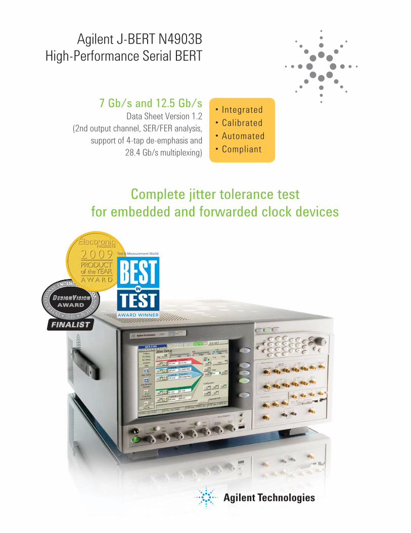
Agilent J-BERT N4903BHigh-Performance Serial BERT
7 Gb/s and 12.5 Gb/sData Sheet Version 1.2
(2nd output channel, SER/FER analysis,
support of 4-tap de-emphasis and
28.4 Gb/s multiplexing)
Complete jitter tolerance test for embedded and forwarded clock devices
• Integrated
• Calibrated
• Automated
• Compliant
Agilent Technologies N4900 Series
Agilent offers a wide range of serial bit error ratio test (BERT)
solutions for R&D and manufacturing. The J-BERT N4903B high-
performance serial BERT is the flagship of Agilent’s N4900 serial
BERT series. It addresses the needs of R&D and validation teams
who characterize serial I/O ports or ASICs up to 14.2 Gb/s.
Integrated and calibrated jitter sources for jitter tolerance measure-
ments also allow designers to characterize and prove compliance
of their receiver’s jitter tolerance.
The B version of the J-BERT has been improved to address the test
needs during characterization and compliance test of emerging
forwarded clock and embedded clock devices in the most complete
and integrated way.
Agilent’s N4900 serial BERT series offers key benefi ts:
• Excellent precision and sensitivity for accurate measurements
• Choice of feature set and frequency classes to tailor to test needs
and budget
• State-of-the-art user interfaces with color touch screen
• Remote control via LAN, USB and GPIB interfaces, compatible
with existing command set Agilent 71612, 81630A Series, N4900
Series
• Small form factor saves rack or bench space
Table 1. Serial BERT applications and selection guide
Device under test Typical requirements Recommended Agilent BERT
For R&D and
characterization
For manufacturing
Optical transceivers or backplanes beyond 14 Gb/s, i.e.:
100GBASE –LR4,-ER4, 32x FC, CEI 25G
• Signal precision
• Data rates > 14 Gb/s
N4903B Options D14,
002 with N4876A
n/a
Optical transceivers, i.e.:
SONET, SDH, 10 GbE, XFP/XFI, SFP+, 16x FC
• PRBS
• Signal precision
• Eye masks
• Data rates > 10 Gb/s
N4903B N4906B-012
or N2101B-300
High-speed serial computer buses, and backplanes, i.e.
QPI, HT, FB-DIMM, PCI Express, USB 3, SATA, SAS,
DisplayPort, CEI, Fibre Channel 4 G/8 G
• Test pattern sequences• CDR• Differential inputs• Data rates < 7 Gb/s
N4903B1 N4906B-012
N4906B-101
N4906B-102
0.6 – 2.5 Gb/s transceiver, i.e. E-PON/ G-PON OLTs,
Gigabit Ethernet, Fibre Channel 1x/2x
• Fast bit synchronization
• Data rates < 3.5 Gb/s
N4906B Option 0031 N5980A
or N2101B-100
1. Or ParBERT 81250 for multi-lane testing
2
3
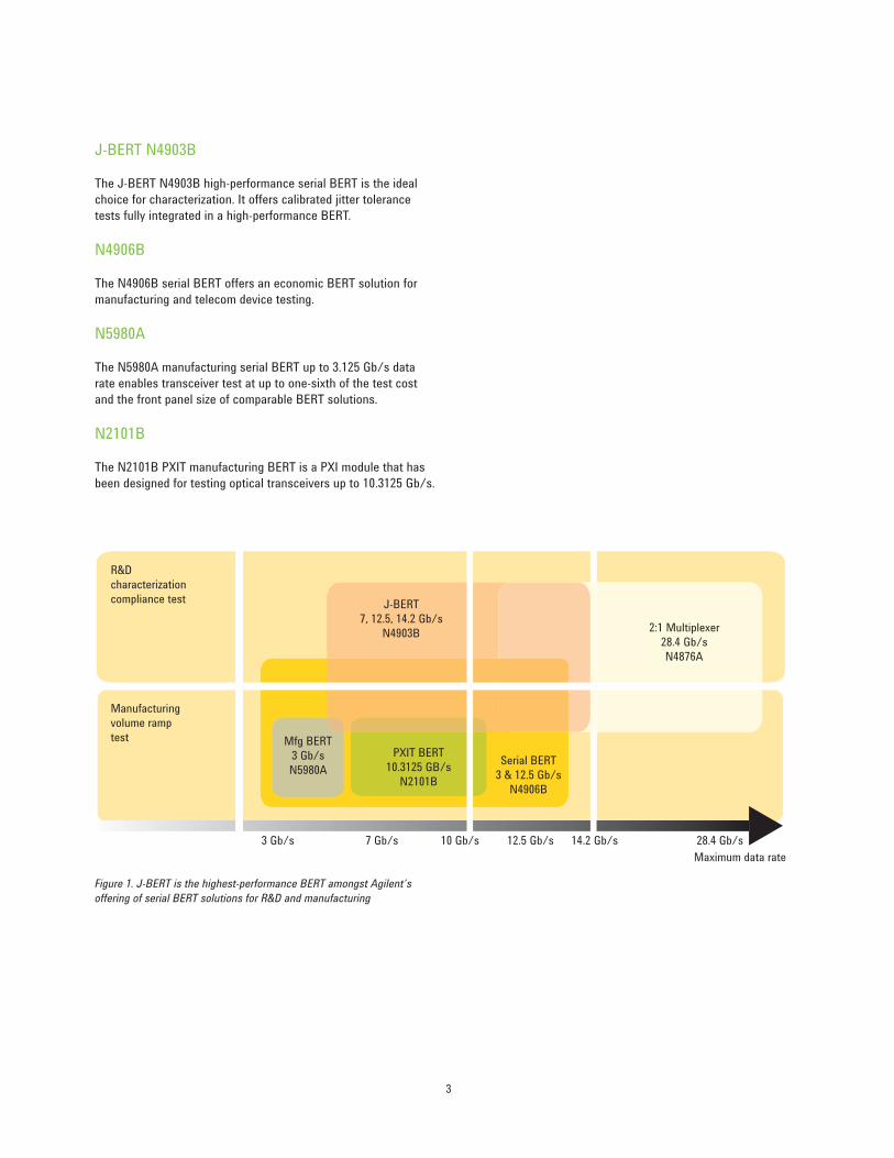
Figure 1. J-BERT is the highest-performance BERT amongst Agilent‘s
offering of serial BERT solutions for R&D and manufacturing
R&D
characterization
compliance test
3 Gb/s 12.5 Gb/s 14.2 Gb/s 28.4 Gb/s7 Gb/s 10 Gb/s
Serial BERT
3 & 12.5 Gb/s
N4906B
Manufacturing
volume ramp
test Mfg BERT
3 Gb/s
N5980A
PXIT BERT
10.3125 GB/s
N2101B
Maximum data rate
2:1 Multiplexer
28.4 Gb/s
N4876A
J-BERT
7, 12.5, 14.2 Gb/s
N4903B
J-BERT N4903B
The J-BERT N4903B high-performance serial BERT is the ideal
choice for characterization. It offers calibrated jitter tolerance
tests fully integrated in a high-performance BERT.
N4906B
The N4906B serial BERT offers an economic BERT solution for
manufacturing and telecom device testing.
N5980A
The N5980A manufacturing serial BERT up to 3.125 Gb/s data
rate enables transceiver test at up to one-sixth of the test cost
and the front panel size of comparable BERT solutions.
N2101B
The N2101B PXIT manufacturing BERT is a PXI module that has
been designed for testing optical transceivers up to 10.3125 Gb/s.

4
J-BERT N4903B High-Performance Serial BERT
The J-BERT N4903B high-performance serial BERT provides the
most complete jitter tolerance test for embedded and forwarded
clock devices.
It is the ideal choice for R&D and validation teams characterizing
and stressing chips and transceiver modules that have serial I/O
ports up to 7 Gb/s, 12.5 Gb/s or even 14.2 Gb/s. It can character-
ize a receiver’s jitter tolerance and is designed to prove compli-
ance to today’s most popular serial bus standards, such as:
• PCI Express
• SATA/SAS
• DisplayPort
• USB SuperSpeed
• Fibre Channel
• QPI
• HyperTransport
• Memory buses, such as fully buffered DIMM2
• Backplanes, such as CEI
• 10 GbE/ XAUI
• XFP/XFI, SFP+
• 100 GbE (10 x 10 or 4 x 27)
Press the Jitter button to set all
jitter parameters you need
Touch screen control of
all J-BERT parameters
Remote operation via LAN, GPIB, USB2
or GUI control via built-in web server
Accurate characterization is achieved with clean signals from the
pattern generator, which features exceptionally low jitter and extremely
fast transition times. Built-in and calibrated jitter sources allow accu-
rate jitter tolerance testing of receivers.
Test set-up is simplified significantly, because the J-BERT N4903B is
designed to match serial bus standards optimally. It offers: differential
I/Os, variable voltage levels on all signal outputs, built-in jitter and ISI,
pattern sequencer, reference clock outputs, tunable CDR, pattern cap-
ture and bit recovery mode to analyze clock-less and non-deterministic
patterns.
5
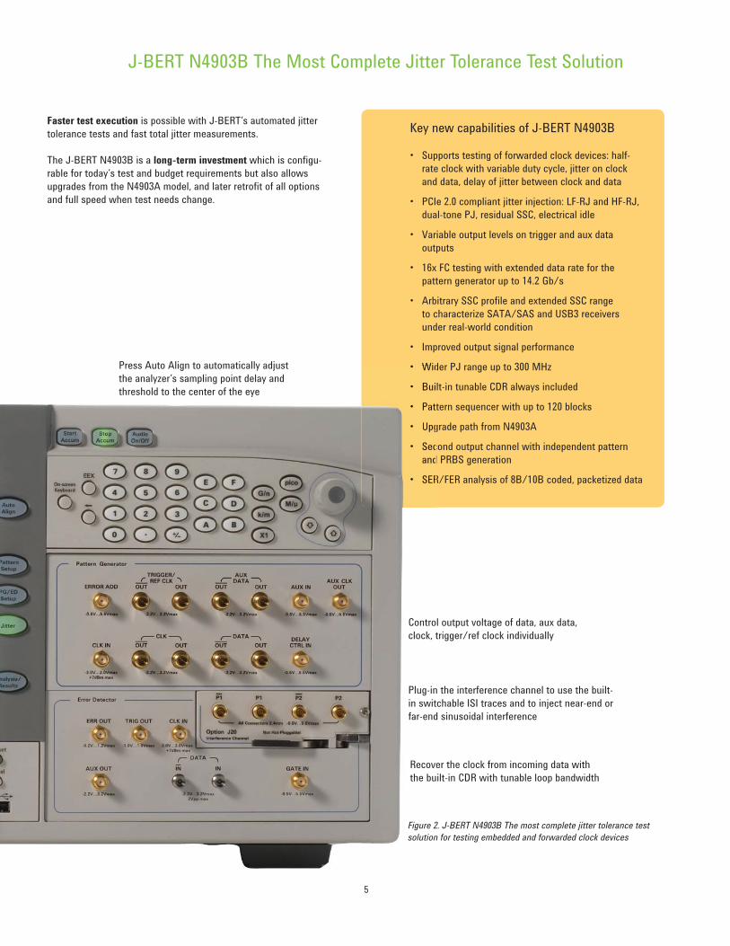
J-BERT N4903B The Most Complete Jitter Tolerance Test Solution
Key new capabilities of J-BERT N4903B
• Supports testing of forwarded clock devices: half-
rate clock with variable duty cycle, jitter on clock
and data, delay of jitter between clock and data
• PCIe 2.0 compliant jitter injection: LF-RJ and HF-RJ,
dual-tone PJ, residual SSC, electrical idle
• Variable output levels on trigger and aux data
outputs
• 16x FC testing with extended data rate for the
pattern generator up to 14.2 Gb/s
• Arbitrary SSC profile and extended SSC range
to characterize SATA/SAS and USB3 receivers
under real-world condition
• Improved output signal performance
• Wider PJ range up to 300 MHz
• Built-in tunable CDR always included
• Pattern sequencer with up to 120 blocks
• Upgrade path from N4903A
• Second output channel with independent pattern
and PRBS generation
• SER/FER analysis of 8B/10B coded, packetized data
• Wid
• Bui
• Pat
• Upg
• Sec
and
• SER
Figure 2. J-BERT N4903B The most complete jitter tolerance test
solution for testing embedded and forwarded clock devices
Press Auto Align to automatically adjust
the analyzer’s sampling point delay and
threshold to the center of the eye
Control output voltage of data, aux data,
clock, trigger/ref clock individually
Recover the clock from incoming data with
the built-in CDR with tunable loop bandwidth
Plug-in the interference channel to use the built-
in switchable ISI traces and to inject near-end or
far-end sinusoidal interference
Faster test execution is possible with J-BERT’s automated jitter
tolerance tests and fast total jitter measurements.
The J-BERT N4903B is a long-term investment which is configu-
rable for today’s test and budget requirements but also allows
upgrades from the N4903A model, and later retrofit of all options
and full speed when test needs change.
6
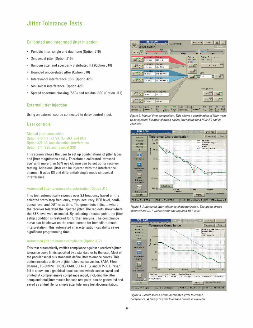
Calibrated and integrated jitter injection
• Periodic jitter, single and dual-tone (Option J10)
• Sinusoidal jitter (Option J10)
• Random jitter and spectrally distributed RJ (Option J10)
• Bounded uncorrelated jitter (Option J10)
• Intersymbol interference (ISI) (Option J20)
• Sinusoidal interference (Option J20)
• Spread spectrum clocking (SSC) and residual SSC (Option J11)
External jitter injection
Using an external source connected to delay control input.
User controls
Manual jitter composition
Option J10: PJ 1 / 2, SJ, RJ, sRJ, and BUJ
Option J20: ISI and sinusoidal interference
Option J11: SSC and residual SSC
This screen allows the user to set up combinations of jitter types
and jitter magnitudes easily. Therefore a calibrated ‘stressed
eye’ with more than 50% eye closure can be set up for receiver
testing. Additional jitter can be injected with the interference
channel. It adds ISI and differential/single mode sinusoidal
interference.
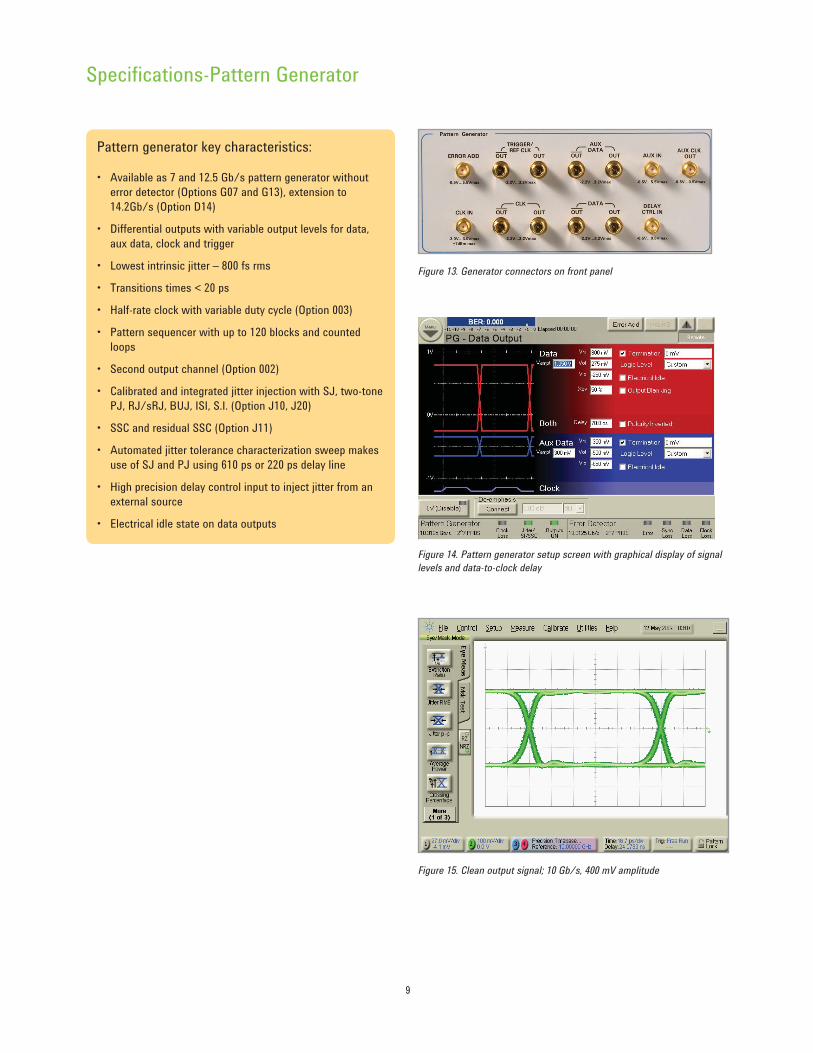
Automated jitter tolerance characterization (Option J10)
This test automatically sweeps over SJ frequency based on the
selected start/stop frequency, steps, accuracy, BER level, confi-
dence level and DUT relax time. The green dots indicate where
the receiver tolerated the injected jitter. The red dots show where
the BER level was exceeded. By selecting a tested point, the jitter
setup condition is restored for further analysis. The compliance
curve can be shown on the result screen for immediate result
interpretation. This automated characterization capability saves
significant programming time.
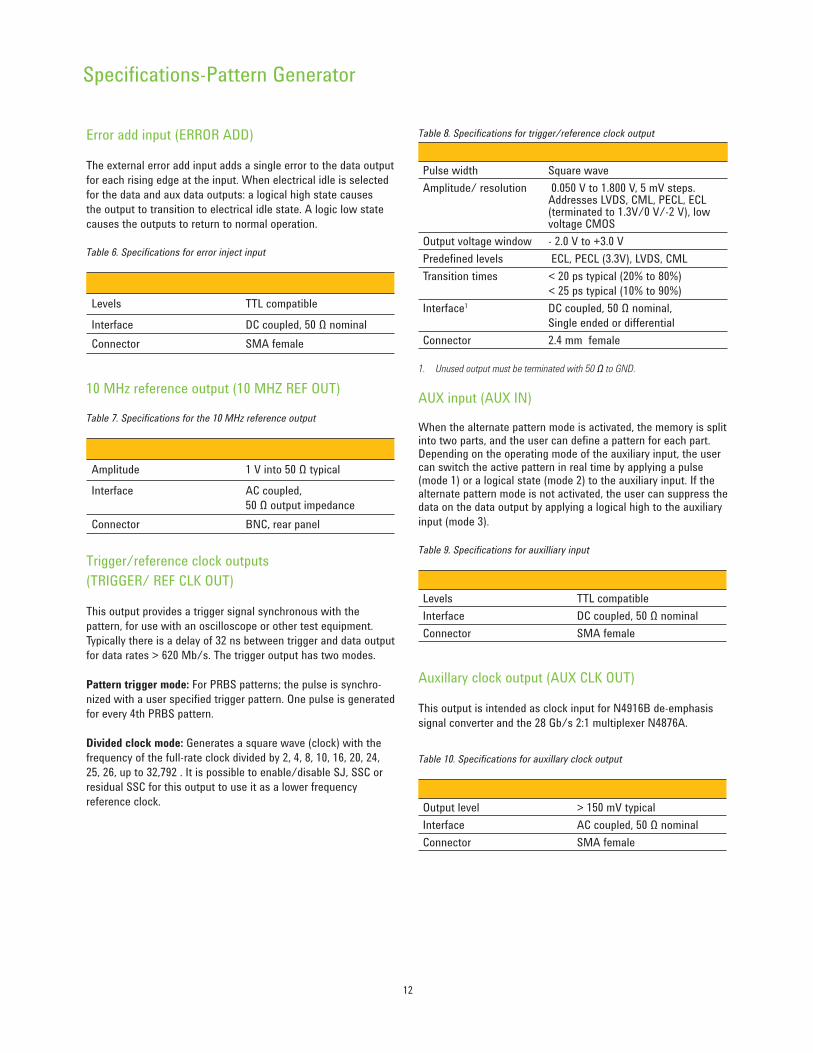
Automated jitter tolerance compliance (Option J12)
This test automatically verifies compliance against a receiver’s jitter
tolerance curve limits specified by a standard or by the user. Most of
the popular serial bus standards define jitter tolerance curves. This
option includes a library of jitter tolerance curves for: SATA, Fibre
Channel, FB-DIMM, 10 GbE/XAUI, CEI 6/11 G, and XFP/XFI. Pass/
fail is shown on a graphical result screen, which can be saved and
printed. A comprehensive compliance report, including the jitter
setup and total jitter results for each test point, can be generated and
saved as a html file for simple jitter tolerance test documentation.
Jitter Tolerance Tests
Figure 3. Manual jitter composition. This allows a combination of jitter types
to be injected. Example shows a typical jitter setup for a PCIe 2.0 add-in
card test
Figure 4. Automated jitter tolerance characterization. The green circles
show where DUT works within the required BER-level
Figure 5. Result screen of the automated jitter tolerance
compliance. A library of jitter tolerance curves is available

7
User Interface and Measurement Suite
Quick eye diagram and masking
The quick eye diagram allows a one-shot check for a valid signal.
Due to the higher sampling depth of a BERT, the eye contour
lines visualize the measured eye at a deeper BER level for more
accurate results. Extrapolated eye contour lines display the eye
opening for even lower BER levels, such as 10-15, reducing the
measurement time significantly. The display shows numerical
results for 1- and 0- level, eye amplitude and width, total jitter
and more. Eye masks can be loaded from a library. Violations of
the captured eye mask are displayed. The result screen can be
printed and saved for documenting the test results (see Figure 6).
Figure 7. Spectral jitter decomposition for debugging jitter sources in a
design.
Figure 8. Eye contour with colors indicating BER level
Figure 6. Quick eye diagram with BER contour and masking
Figure 9. BERT scan including RJ/DJ separation, total jitter
Spectral jitter decomposition
The spectral jitter decomposition measures the spectral decom-
position of jitter components. When debugging designs, the jitter
decomposition simplifies identifying deterministic jitter sources
(see Figure 7).
Eye contour
The eye opening is a key characteristic of a device. The BER is
displayed as a function of sampling delay and sampling threshold.
Different views are available: eye contour (see Figure 8), pseudo
colors and equal BER plots.
BERT scan including RJ/DJ separation
This measurement shows the BER versus the sampling point
delay, which is displayed as a “bathtub” curve or as a histogram.
The measurement results are displayed in a table with setup and
hold time over phase margin, total jitter in rms or peak-to-peak,
and random and deterministic jitter. The measurement method is
equivalent to IEEE 802.3ae (see Figure 9).

8
User Interface
Bit recovery mode (Option A01)
This mode is useful for analyzing non-deterministic traffic. This is
helpful when you need to analyze real world traffic, for example in
a PCI Express link, where so-called ‘skip ordered sets’ are added
unpredictably to avoid FIFO overflow. This simplifies setup by
eliminating the need to setup expected data for the error detector.
Two analyzer sampling points are used to measure a relative BER,
which makes the following measurements possible with relative
BER:
• BERT scan including RJ/DJ separation
• Output levels and Q factor
• Eye contour
• Fast eye mask
• Fast total jitter
• Spectral jitter decomposition
Automatic alignment
The J-BERT is able to align the voltage threshold and the delay
offset of the sampling point automatically, either simultaneously
or separately. It is possible to search for the 0/1 threshold
automatically on command, and to track the 0/1 threshold
continuously (see Figure 11).
Fast total jitter
Agilent implemented a new measurement technique for TJ (BER),
the fast total jitter measurement. This method provides fast and
feasible total jitter measurements, around 40 times faster than
a common BERT scan but with comparable confidence level.
Instead of comparing bits until the BER reaches a defined number
of bits or a defined number of errors, it only compares bits until it
can decide with a 95% confidence level whether the actual BER
is above or below the desired BER (see Figure 12).
Web-based access to GUI
J-BERT can be operated conveniently from any remote web
location with the built-in web server. So even without program-
ming knowledge, J-BERT can be operated and monitored from a
distance or off-site and in noisy or environmental test labs.
Figure 10. Bit recovery mode for analyzing non-deterministic traffi c
Figure 11. Auto alignment (center) simplifi es correct sampling
Figure 12. Fast total jitter measurement for quick and accurate total jitter
measurements
9
Figure 14. Pattern generator setup screen with graphical display of signal
levels and data-to-clock delay
Specifi cations-Pattern Generator
Figure 13. Generator connectors on front panel
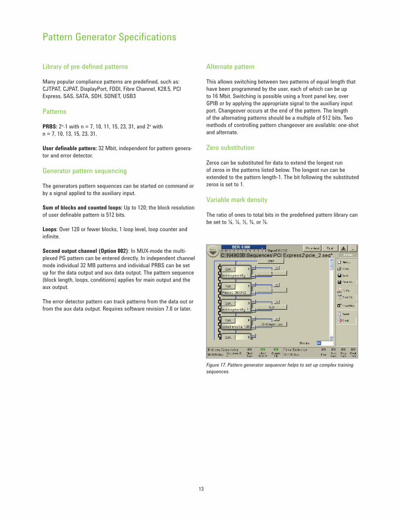
Pattern generator key characteristics:
• Available as 7 and 12.5 Gb/s pattern generator without
error detector (Options G07 and G13), extension to
14.2Gb/s (Option D14)
• Differential outputs with variable output levels for data,
aux data, clock and trigger
• Lowest intrinsic jitter – 800 fs rms
• Transitions times < 20 ps
• Half-rate clock with variable duty cycle (Option 003)
• Pattern sequencer with up to 120 blocks and counted
loops
• Second output channel (Option 002)
• Calibrated and integrated jitter injection with SJ, two-tone
PJ, RJ/sRJ, BUJ, ISI, S.I. (Option J10, J20)
• SSC and residual SSC (Option J11)
• Automated jitter tolerance characterization sweep makes
use of SJ and PJ using 610 ps or 220 ps delay line
• High precision delay control input to inject jitter from an
external source
• Electrical idle state on data outputs
Figure 15. Clean output signal; 10 Gb/s, 400 mV amplitude

Specifi cations-Pattern Generator
Data output and auxiliary data output (DATA OUT, AUX DATA OUT)
Table 2. Output characteristics for J-BERT N4903B generator. All timing parameters are measured at ECL levels.
Range of operation 5 150 Mb/s to 14.2 Gb/s (Option D14, required in addition to C13 or G13)
150 Mb/s to 12.5 Gb/s (Option C13 or G13); can be programmed up to 13.5 Gb/s
150 Mb/s to 7 Gb/s (Option C07 or G07);
< 620 MHz only with external clock
Frequency accuracy ± 15 ppm typical
Format NRZ, normal or inverted
Electrical idle Output transitions from full swing signal to 0 V amplitude and vice versa at constant offset within 4 ns typ. Electrical
idle is controlled by the error add input connector
Amplitude/resolution 0.050 V to 1.800 V, 5 mV steps; addresses LVDS, CML, PECL, ECL (terminated to 1.3 V/0 V/-2 V), low voltage CMOS
Output voltage window - 2.0 V to +3.0 V
Predefi ned levels ECL (-2V), SCFL (0V), LVPECL (1.3V), LVDS (1.25V), and CML (0V)
Transition times
20% to 80%
10% to 90% 1
< 20 ps
< 25 ps
Intrinsic jitter 4 9 ps pp typical with internal clock
Clock/data delay range ± 0.75 ns in 100 fs steps
Auto-calibration possible to compensate for temperature drifts
External termination voltage 2 - 2 V to +3 V
Crossing point Adjustable 20% to 80% typical to emulate duty cycle distortions
AUX data modes: • Sub-rate clock mode: can be used to generate lower rate reference clocks with divider factor
n = 2, 3, 4, 5, ... 128 relative to data rate. This is the same function as the sub-rate clock output of N4903A.
• Pattern and PRBS generation (Option 002). Can be used to drive a multiplexer such as N4876A
(requires SW 6.7 or later) and as independent second data channel (requires SW 7.0 or later).
Skew < 15 ps typical between data output and aux data output
Single error inject Adds single errors on demand
Fixed error inject Fixed error ratios of 1 error in 10n bits, n = 3, 4, 5, 6, 7, 8, 9
Interface 3 Differential or single-ended, DC coupled, 50 Ω
Connector 2.4 mm female
1. At 10 Gb/s and 7 Gb/s
2. For positive termination voltage or termination to GND, external termination voltage must be less than 3 V below VOH. For negative termination voltage, external termination
voltage must be less than 2 V below VOH. External termination voltage must be less than 3 V above VOL.
3. Unused outputs must be terminated with 50 Ω to GND.
4. At target BER 10 -9, with PRBS 2 31, 10 Gb/s
5. When Option D14 is enabled, and data rates are > 12.5 Gb/s: PJ1 + PJ2 range 0 to 2.0 UI, modulation frequency range 1 kHz to 100 MHz. RJ range 0 to 20 mUI rms
(0 to 280 mUI pp). For BUJ, functionality is not guaranteed and might require manual calibration. For data rates > 13.5 Gb/s SSC, SJ are disabled.
10

11
Pattern Generator Specifi cations
Clock output (CLK OUT)
Clock can operate at full bit-rate or at half bit-rate (Option 003) to
support testing of forward clocked devices.
Table 3. Clock output specifi cations
Frequency range 150 MHz to 14.2 GHz (Option D14,
in addition to C13 or G13);
150 MHz to 12.5 GHz (Option C13 or G13);
can be programmed up to 13.5 GHz
150 MHz to 7 GHz (Option C07 or G07);
< 620 MHz only with external clock
Half-rate clocking Only with Option 003: Available at bit rates
> 2.7 Gb/s; duty cycle on half-rate clock
adjustable 40% to 60%
Amplitude/resolution 0.050 V pp to 1.800 V pp, 5 mV steps
Output voltage window -2.00 to +3.00 V
Transition times
20% to 80%
10% to 90% 1
< 20 ps
< 25 ps
External termination
voltage
-2 V to +3 V
Jitter 800 fs rms typical with internal clock
SSB phase noise < -75 dBc with internal clock source, 10 GHz
at 10 kHz offset, 1 Hz bandwidth
Interface 3 Differential or single-ended, DC coupled,
50 Ω output impedance
Connector 2.4 mm female
1. At 10 Gb/s and 7 Gb/s
2. For positive termination voltage or termination to GND, external termination voltage must be less than 3 V below VOH. For negative termination voltage, external termination voltage must be less than 2 V below VOH. External termination volt age must be less than 3 V above VOL.
3. Unused outputs must be terminated with 50 Ω to GND.
Clock input (CLK IN)
There are two modes when using the clock input connector.
1. External clock mode: all output signals follow the external clock and its modulation. The modulation of the external clock must be within the same range given for SSC and SJ (see Table 12). If the external clock is above 6.75 GHz, all internal jitter sources can be used (for using 610 ps delay line, external clock divider z = 4). Below 6.75 GHz, SJ and SSC are not avail-able. However, the external clock can optionally be divided by 1, 2, 4, 8, or 16, provided that the resulting bit rate does not fall below 150 Mb/s. Modulation using the 220 ps delay line is still available (see Figure 22).
2. External PLL mode: it is used to lock the generator to an external clock. The provided clock must not be modulated in external PLL mode. All internal jitter sources are available. A clock multiplication with x/y is possible, with x, y = 1,2,3, to 255. The resulting bit rate has to be within the range 620 Mb/s
to maximum bit rate.
External clock
10 M H z ref clock
Internal clock
External clock(PLL m ode)
C lock generatorz = 1,2,4,8,16,
resulting bit rate
must be > 150 Mb/s
VCOVCO
PLLPLL
1/z1/z
Clock
source
selection
x/y
Figure 16. N4903B supports multiple clock modes
10 MHz reference input (10 MHz REF IN)
This is used to lock the generator to an external 10 MHz reference
clock. The data rate can be selected within the same range as if
the internal clock would be used. The provided reference clock
must not be modulated. All internal jitter sources are available.
Table 4. Specifi cations for clock input and 10 MHz reference input
Amplitude 200 mV to 2 V
Frequency CLK IN: 150 MHz to 12.5 GHz
(14.2 GHz for Option D14)
10 MHz REF IN: 10 MHz
Interface AC coupled, 50 Ω nominal
Connectors
Clock input
10 MHz reference input
SMA female, front panel
BNC, rear panel
Delay control input (DELAY CTRL IN)
The external signal applied to delay control input varies the delay
between data output and clock output. This can be used to gener-
ate jittered signals to stress the device under test in addition to
the calibrated jitter injection from N4903B.
Table 5. Specifi cations for delay control input
Range -110 ps to +110 ps
Sensitivity Typical
Linearity ±5% typical
Modulation bandwidth 1 GHz typical at 10.8 Gb/s
data rate
Levels -275 mV to +275 mV
Interface DC coupled, 50 Ω nominal
Connector SMA female
12
Error add input (ERROR ADD)
The external error add input adds a single error to the data output
for each rising edge at the input. When electrical idle is selected
for the data and aux data outputs: a logical high state causes
the output to transition to electrical idle state. A logic low state
causes the outputs to return to normal operation.
Table 6. Specifi cations for error inject input
Levels TTL compatible
Interface DC coupled, 50 Ω nominal
Connector SMA female
10 MHz reference output (10 MHZ REF OUT)
Table 7. Specifi cations for the 10 MHz reference output
Amplitude 1 V into 50 Ω typical
Interface AC coupled,
50 Ω output impedance
Connector BNC, rear panel
Specifi cations-Pattern Generator
Table 8. Specifi cations for trigger/reference clock output
Pulse width Square wave
Amplitude/ resolution 0.050 V to 1.800 V, 5 mV steps. Addresses LVDS, CML, PECL, ECL (terminated to 1.3V/0 V/-2 V), low voltage CMOS
Output voltage window - 2.0 V to +3.0 V
Predefined levels ECL, PECL (3.3V), LVDS, CML
Transition times < 20 ps typical (20% to 80%)
< 25 ps typical (10% to 90%)
Interface1 DC coupled, 50 Ω nominal,
Single ended or differential
Connector 2.4 mm female
1. Unused output must be terminated with 50 Ω to GND.
AUX input (AUX IN)
When the alternate pattern mode is activated, the memory is split into two parts, and the user can define a pattern for each part. Depending on the operating mode of the auxiliary input, the user can switch the active pattern in real time by applying a pulse (mode 1) or a logical state (mode 2) to the auxiliary input. If the alternate pattern mode is not activated, the user can suppress the data on the data output by applying a logical high to the auxiliary
input (mode 3).
Table 9. Specifi cations for auxilliary input
Levels TTL compatible
Interface DC coupled, 50 Ω nominal
Connector SMA female
Trigger/reference clock outputs
(TRIGGER/ REF CLK OUT)
This output provides a trigger signal synchronous with the
pattern, for use with an oscilloscope or other test equipment.
Typically there is a delay of 32 ns between trigger and data output
for data rates > 620 Mb/s. The trigger output has two modes.
Pattern trigger mode: For PRBS patterns; the pulse is synchro-
nized with a user specified trigger pattern. One pulse is generated
for every 4th PRBS pattern.
Divided clock mode: Generates a square wave (clock) with the
frequency of the full-rate clock divided by 2, 4, 8, 10, 16, 20, 24,
25, 26, up to 32,792 . It is possible to enable/disable SJ, SSC or
residual SSC for this output to use it as a lower frequency
reference clock.
Auxillary clock output (AUX CLK OUT)
This output is intended as clock input for N4916B de-emphasis
signal converter and the 28 Gb/s 2:1 multiplexer N4876A.
Table 10. Specifi cations for auxillary clock output
Output level > 150 mV typical
Interface AC coupled, 50 Ω nominal
Connector SMA female
13
Library of pre-defi ned patterns
Many popular compliance patterns are predefined, such as:
CJTPAT, CJPAT, DisplayPort, FDDI, Fibre Channel, K28.5, PCI
Express, SAS, SATA, SDH, SONET, USB3
Patterns
PRBS: 2n-1 with n = 7, 10, 11, 15, 23, 31, and 2n with
n = 7, 10, 13, 15, 23, 31.
User definable pattern: 32 Mbit, independent for pattern genera-
tor and error detector.
Generator pattern sequencing
The generators pattern sequences can be started on command or
by a signal applied to the auxiliary input.
Sum of blocks and counted loops: Up to 120; the block resolution
of user definable pattern is 512 bits.
Loops: Over 120 or fewer blocks, 1 loop level, loop counter and
infinite.
Second output channel (Option 002): In MUX-mode the multi-
plexed PG pattern can be entered directly. In independent channel
mode individual 32 MB patterns and individual PRBS can be set
up for the data output and aux data output. The pattern sequence
(block length, loops, conditions) applies for main output and the
aux output.
The error detector pattern can track patterns from the data out or
from the aux data output. Requires software revision 7.0 or later.
Pattern Generator Specifi cations
Figure 17. Pattern generator sequencer helps to set up complex training
sequences.
Alternate pattern
This allows switching between two patterns of equal length that
have been programmed by the user, each of which can be up
to 16 Mbit. Switching is possible using a front panel key, over
GPIB or by applying the appropriate signal to the auxiliary input
port. Changeover occurs at the end of the pattern. The length
of the alternating patterns should be a multiple of 512 bits. Two
methods of controlling pattern changeover are available: one-shot
and alternate.
Zero substitution
Zeros can be substituted for data to extend the longest run
of zeros in the patterns listed below. The longest run can be
extended to the pattern length-1. The bit following the substituted
zeros is set to 1.
Variable mark density
The ratio of ones to total bits in the predefined pattern library can
be set to ⅛ , ¼ , ½ , ¾ , or ⅞ .

14
Sine wave
For all data rates
For data rates 1 s
Data rate x 220 ps
3000 001 20 100
1 0*
* 220 ps max
Sine wavetriangularsquare wave
Jitter amplitude
(UI)
Modulation frequency (MHz)
Jitter Tolerance Test Specifi cations
The built-in jitter sources are designed to cover DisplayPort,
PCI Express, SATA, USB3, Fibre Channel, QPI, Hypertransport,
FB-DIMM, CEI 6 G/11 G, 10 GbE and XFP/XFI, SFP+ jitter toler-
ance test needs.
Periodic jitter (Option J10)
This injects sinusoidal, rectangular
or triangular jitter over a wide
frequency range.
Table 11. Specifi cations for periodic jitter (PJ1, PJ2)
Range1 0 to 220 ps pp at all data rates
0 to 610 ps pp at data rates
≤ 3.375 Gb/s
Modulation frequency
Sine
One- and two-tone possible
1 kHz to 300 MHz
Triangle/square 1 kHz to 20 MHz
Modulation frequency
accuracy
0.5% ± 25 Hz typical
Jitter amplitude accuracy 10% ± 1 ps typical
Impacted signals 610 ps delay line: only on data and aux
data outputs
220 ps delay line: user selectable for
data and aux data outputs, clock output
Jitter delay 0 to ±2.2 ns, 100 ps steps between
jitter on data and aux data output
versus jitter on clock output for all jitter
sources using the 220 ps delay line.
1. Available range depends on modulation frequency and data rate
(see Figures 18 and 19).
Figure 19. Periodic jitter maximum using the 220 ps delay line
Figure 18. Periodic jitter maximum for data rates ≤ 3.375 Gb/s using the
610 ps delay line
Jitter
amplitude
(UI)
Modulation frequency (MHz)
300 80
1.1*
Sine waveSine wave,trinagular,
square waveData
rate x 610 ps
0.001 20 250
0.5*
* 610 ps max.
SSC – spread spectrum clocking (Option J11)
The built-in SSC clock modulation source is available only in combi-nation with Option J10. It either generates a frequency modulated clock signal (SSC) or a phase modulated clock signal (residual SSC) as used in some computer or storage standards such as PCIe, USB and SATA to spread EMI. If residual SSC is enabled, sinusoidal jitter is not available, however all other jitter sources can be used. If SSC is enabled, sinusoidal jitter is available in a limited range, however all other jitter sources can be used without restrictions. SSC (% of
max) + SJ (% of max) ≤ 100%.
Table 12. Spread spectrum clocking (SSC) characteristics
SSC frequency deviation:
up-spread/down-spread
0 to -0.5% (5,000 ppm),
2% typical accuracy
SSC frequency deviation:
center-spread
0 to 1.0% pp (10,000 ppm),
2 % typical accuracy. Can be
used also for down-spread
SSC, allowing more SJ range
Residual SSC phase modulation 0 to 100 ps
Modulation frequency 100 Hz to 100 kHz
Modulation waveform Triangular or arbitrary.
Arbitrary files can be uploaded
as txt file. Values from -1.0 to
+1.0 for 1.0% center-spread
modulation, maximum of
16384 data points
Signals impacted Can be enabled for either data and aux data output and/or clock output and trigger/ref clock out

15
Sinusoidal jitter (Option J10)
This injects sinusoidal jitter in the lower
frequency range with multiple UIs.
Table 13. Specifi cations for sinusoidal jitter (SJ)
Range1 2 UI at 5 MHz
1000 UI at 10 kHz
For frequencies between 10 kHz and
5 MHz the jitter amplitude
= UI
Modulation frequency 100 Hz to 5 MHz (For higher modulation
frequencies, see Table 10)
Modulation frequency
accuracy
0.5% typical
Jitter amplitude accuracy 2% ± 1 ps typical
Impacted signals User selectable for data and aux data
outputs, clock output and trigger/ref
clock output.
1. Available range depends on modulation frequency and data rate
(see Figure 20).
10 MHz
n x f (mod)
Jitter Tolerance Test Specifi cations
Figure 20. Sinusoidal jitter maximum UI
100 Hz 10 kHz 5 MHz
2UI
n
Modulation
frequency
Jitter
amplitude
(UI)
1000 UI
n
Data rate n
Max UI at
modulation
frequency
100 Hz to 10 kHz
Max UI at
modulation
frequency
5 MHz
6.75 Gb/s to 12.5 Gb/s n = 1 1000 UI 2 UI
3.375 Gb/s to 6.75 Gb/s n = 2 500 UI 1 UI
1.6875 Gb/s to 3.375 Gb/s n = 4 250 UI 0.5 UI
843,75 Mb/s to 1.6875 Gb/s n = 8 125 UI 0.25 UI
620 Mb/s to 843.75 Mb/s n = 16 62.5 UI 0.125 UI
Random jitter (Option J10)
This injects random jitter with a high band-
width and excellent crest factor.
It also allows injecting a spectrally distrib-
uted random jitter profile, as required for
PCIe 2.0 receiver test.
Table 14. Specifi cations for random jitter (RJ)
Range • 0 to 15.7 ps rms (0 to 220 ps pp) at
data rates < 8.1 Gb/s
• 0 to 72 mUI (0 to 1UI pp) at data
rates ≥ 8.1 Gb/s
• 0 to 8 ps rms ( 0 to 112 ps pp) if
100 MHz low-pass fi lter is turned on
sRJ If spectrally distributed random jitter
(sRJ) is used, the same limits apply to
the square root sum of LF-RJ and HF-
RJ components. See Figure 21.
Crest factor 14 (pp to rms ratio)
Bandwidth 50 kHz to 1 GHz
Filter • 10 MHz high-pass
• 100 MHz low-pass
• 500 MHz low-pass
Can be turned on or off individually to
limit jitter bandwidth
Jitter amplitude accuracy 10% ± 0.2 ps typical
Figure 21. Spectrally distributed RJ allows to inject low frequency and
high frequency RJ: this is required for compliant PCIe 2 receiver testing
Modula tion frequency
100 MHz 1 GHz10 kH z
R J-H F
R J-LF
1.5 M H z
R J jitte r amplitude
(ps rms/ Hz)
16
Bounded uncorrelated jitter (Option J10)
This injects a high probability jitter using a
PRBS generator and low-pass filters.
Table 15. Specifi cations for bounded uncorrelated jitter (BUJ)
Range 0 to 1.1 UI (not to exceed capabilitiy of
delay line used)
PRBS polynomials 2n-1; n = 7, 8, 9, 10, 11, 15, 23, 31
Data rate of PRBS generator 200 Mb/s to 3.2 Gb/s
Filters 50/100/200 MHz lowpass 3rd order
Jitter amplitude accuracy 10% ± 1 ps typical for settings shown
in Table 15.
Jitter Tolerance Test Specifi cations
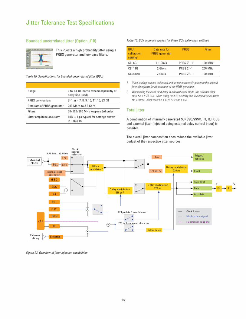
Figure 22. Overview of jitter injection capabilities
Table 16. BUJ accuracy applies for these BUJ calibration settings
BUJ
calibration
setting1
Data rate for
PRBS generator
PRBS Filter
CEI 6G 1.1 Gb/s PRBS 29 - 1 100 MHz
CEI 11G 2 Gb/s PRBS 211-1 200 MHz
Gaussian 2 Gb/s PRBS 231-1 100 MHz
1. Other settings are not calibrated and do not necessarily generate the desired
jitter histograms for all datarates of the PRBS generator.
2. When using the clock modulator in external clock mode, the external clock
must be > 6.75 GHz. When using the 610 ps delay line in external clock mode,
the external clock must be > 6.75 GHz and z = 4.
sR J
PJ1
R J
BU J
Externaldelay
+
+
+
220 ps data & aux data on
220 ps forw arded clock on
C lock
Trigger/
ref clock
Data
Aux data
Clock & data
M odulation signal
F unctional coupling
rSSC
SSC
SJ
PJ2
Internal clock oscillator
PLL
6.75 Gb/s ... 12.5 Gb/s
External clock
C lock source selection
x/y
1/z
Aux clock
1/1 or 1/2
1/n
C lock
modulator 2D elay modulation
220 ps
ISI
P1 P2
Jitter delay
D elay modulation
610 ps 2
D elay modulation
220 ps S.I.+
External
Total jitter
A combination of internally generated SJ/SSC/rSSC, PJ, RJ, BUJ
and external jitter (injected using external delay control input) is
possible.
The overall jitter composition does reduce the available jitter
budget of the respective jitter sources.
17
Jitter Tolerance Test Specifi cations
Figure 23. Interference channel connectors Figure 24. Typical S21 parameter for ISI channel of 9 inch length
Table 18. Typical ISI (measured in UI) for traces depending on data rate, pattern and trace length.
Data rate 1.25 Gb/s 2.5 Gb/s 3.125 Gb/s 5 Gb/s 6.25 Gb/s 11 Gb/s
ISI trace
length
PRBS
27-1
PRBS
215-1
CJPAT PRBS
27-1
PRBS
215-1
CJPAT PRBS
27-1
PRBS
215-1
CJPAT PRBS
27-1
PRBS
215-1
CJPAT PRBS
27-1
PRBS
215-1
CJPAT PRBS
27-1
PRBS
215-1
CJPAT
3.5 inches 0.007 0.017 0.016 0.016 0.022 0.014 0.020 0.031 0.029 0.037 0.062 0.038 0.054 0.085 0.056 0.099 0.146 0.131
9 inches 0.026 0.034 0.037 0.039 0.066 0.039 0.057 0.080 0.079 0.104 0.157 0.092 0.147 0.216 0.138 0.329 0.504 0.405
16 inches 0.045 0.068 0.051 0.103 0.138 0.106 0.137 0.191 0.117 0.279 0.365 0.260 0.346 0.543 0.376
20 inches 0.058 0.088 0.062 0.152 0.184 0.123 0.181 0.276 0.167 0.366 0.529 0.349 0.580
24 inches 0.081 0.109 0.103 0.182 0.260 0.171 0.254 0.356 0.274 0.529
28 inches 0.098 0.141 0.147 0.241 0.334 0.238 0.319 0.483 0.373
32 inches 0.128 0.153 0.120 0.289 0.395 0.295 0.389 0.570 0.376
36 inches 0.156 0.188 0.168 0.375 0.493 0.390 0.507
40 inches 0.172 0.228 0.199 0.458 0.626 0.423 0.617
44 inches 0.199 0.262 0.247 0.571
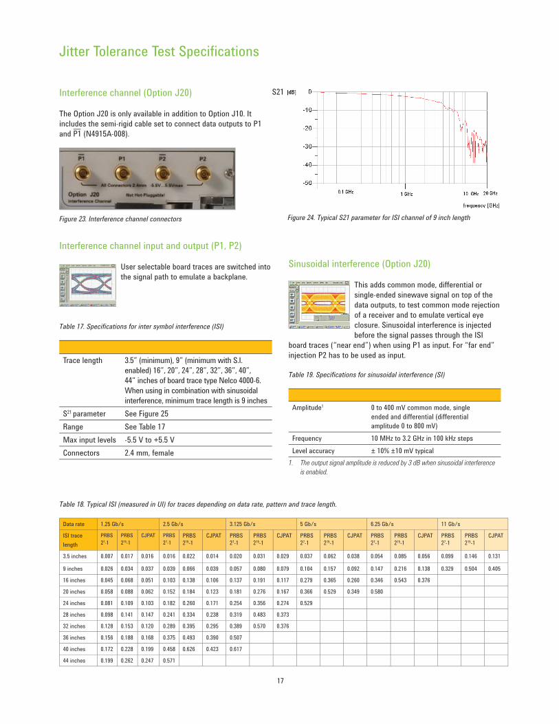
Sinusoidal interference (Option J20)
This adds common mode, differential or
single-ended sinewave signal on top of the
data outputs, to test common mode rejection
of a receiver and to emulate vertical eye
closure. Sinusoidal interference is injected
before the signal passes through the ISI
board traces (“near end”) when using P1 as input. For “far end”
injection P2 has to be used as input.
Table 19. Specifi cations for sinusoidal interference (SI)
Amplitude1 0 to 400 mV common mode, single
ended and differential (differential
amplitude 0 to 800 mV)
Frequency 10 MHz to 3.2 GHz in 100 kHz steps
Level accuracy ± 10% ±10 mV typical
1. The output signal amplitude is reduced by 3 dB when sinusoidal interference
is enabled.
S21Interference channel (Option J20)
The Option J20 is only available in addition to Option J10. It
includes the semi-rigid cable set to connect data outputs to P1
and P1 (N4915A-008).
Interference channel input and output (P1, P2)
User selectable board traces are switched into
the signal path to emulate a backplane.
Table 17. Specifi cations for inter symbol interference (ISI)
Trace length 3.5” (minimum), 9” (minimum with S.I.
enabled) 16”, 20”, 24”, 28”, 32”, 36”, 40”,
44” inches of board trace type Nelco 4000-6.
When using in combination with sinusoidal
interference, minimum trace length is 9 inches
S21 parameter See Figure 25
Range See Table 17
Max input levels -5.5 V to +5.5 V
Connectors 2.4 mm, female
18
Error Detector Specifi cations
Data inputs (DATA IN)
Table 20. Specifi cations for error detector
Range of operation 150 Mb/s to 12.5 Gb/s (Option C13)
150 Mb/s to 7 Gb/s (Option C07)
Format NRZ
Max. input amplitude 2.0 V
Termination voltage 1 -2 V to +3 V or off
true differential mode
Sensitivity 2 < 50 mV pp
Intrinsic transition time 3 25 ps typical 20% to 80%, single ended
Decision threshold range -2 V to +3 V in 1 mV steps
Maximum levels -2.2 V to +3.2 V
Phase margin 4 1 UI – 12 ps typical
Clock-to-data
sampling delay
±0.75 ns in 100 fs steps
Interface Single-ended: 50 Ω nominal,
differential: 100 Ω nominal
Connector 2.4 mm female
1. Clock/data sampling delay range selectable 2 V operating voltage window,
which is in the range between
-2.0 V to +3.0 V. The data signals, termination voltage and decision threshold
have to be within this voltage window.
2. At 10 Gb/s, BER 10-12, PRBS 231-1. For input levels < 100 mV manual threshold
value adjustments may be required.
3. At cable input, at ECL levels.
4. Based on the internal clock.
Error detector key characteristics:
• True differential inputs to match today’s ports
• Built-in CDR with tunable loop-bandwidth up to 12 MHz
• Auto-alignment of sampling point
• Bit recovery mode for unknown data traffic (Option AO1)
• SER/FER analysis of coded and retimed data (Option A02)
• Burst mode for testing recirculating loop
• BER result and measurement suite
• Quick eye diagram and mask with BER contours
Clock inputs (CLK IN)
The error detector requires an external clock signal to sample
data or it can recover the clock from the data signal using the
built-in clock data recovery (CDR).
Table 21. Specifi cation for the clock input
Frequency range 150 MHz to 12.5 GHz (Option
C13); 150 MHz to 7 GHz
(Option C07)
Amplitude 100 mV to 1.2 V
Sampling Positive or negative
clock edge
Interface AC coupled, 50 Ω nominal
Connector SMA female
Clock data recovery
The error detector can recover the clock from the incoming data
stream with the built-in clock data recovery (CDR). The tunable
loop bandwidth comes with N4903A Options C07 and C13. The
recovered clock signal is available at the aux output.
Table 22. Specifi cations for the clock data recovery (Options C07, C13)
Input data rate 1 Gb/s to 12.5 Gb/s1 (Option C13)
1 Gb/s to 7 Gb/s (Option C07)
CDR clock output jitter 0.01 UI rms (RJ) typical 2
Interface AC coupled, 50 Ω nominal
Connector SMA female
1. With bit recovery mode (Option A01) enabled the max data rate is 11.5 Gb/s.
2. When measured with PRBS 223-1
Figure 25. Front panel connectors for error detection
19
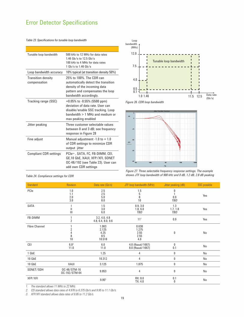
Table 23. Specifi cations for tunable loop bandwidth
Tunable loop bandwidth 500 kHz to 12 MHz for data rates
1.46 Gb/s to 12.5 Gb/s
100 kHz to 4 MHz for data rates
1 Gb/s to 1.46 Gb/s
Loop bandwidth accuracy 10% typical (at transition density 50%)
Transition density
compensation
25% to 100%. The CDR can
automatically detect the transition
density of the incoming data
pattern and compensates the loop
bandwidth accordingly.
Tracking range (SSC) +0.05% to -0.55% (5500 ppm)
deviation of data rate. User can
disable/enable SSC tracking. Loop
bandwidth > 1 MHz and medium or
max peaking enabled
Jitter peaking Three customer selectable values
between 0 and 3 dB; see frequency
response in Figure 28
Fine adjust Manual adjustment -1.0 to + 1.0
of CDR settings to minimize CDR
output jitter
Compliant CDR settings PCIeTM , SATA, FC, FB-DIMM, CEI,
GE,10 GbE, XAUI, XFP/XFI, SONET
OC-48/192 (see Table 23). User can
add own CDR settings
Error Detector Specifi cations
Loop
bandwidth
(MHz)
Tunable loop bandwidth
Data rate
(Gb/s)12.511.51.461.0
0.50.1
4.0
7.5
12.0
Figure 26. CDR loop bandwidth
Figure 27. Three selectable frequency response settings. The example
shows JTF loop bandwidth of 900 kHz and 0 dB, 1.2 dB, 2.8 dB peakingTable 24. Compliance settings for CDR
Standard Revision Data rate (Gb/s) JTF loop bandwidth (MHz) Jitter peaking (dB) SSC possible
PCIe 1.01.12.03.0
2.52.55.08.0
1.55810
01
0.9TBD
Yes
SATA IIIIII
1.53.06.0
0.9, 3.01.8, 6.0
TBD
1.31.7, 1.8
TBDYes
FB-DIMM 12
3.2, 4.0, 4.84.8, 6.4, 8.0, 9.6
111 0.9 Yes
Fibre Channel 124810
1.0632.1254.258.5
10.518
0.6381.2752.552.554.0
0 No
CEI 6.02
11.06.011.0
4.0 (fbaud/1667)8.0 (fbaud/1667)
00.1
No
1 GbE 1.25 4 0 No
10 GbE 10.312 4 0 No
10 GbE XAUI 3.125 1.875 0 No
SONET/SDH OC-48/STM-16OC-192/STM-64
9.953 4 0 No
XFP/XFI9.953 RX: 8.0
TX: 4.00.10
No
1. The standard allows 11 MHz to 22 MHz.
2. CEI standard allows data rates of 4.976 to 6.375 Gb/s and 9.95 to 11.1 Gb/s.
3. XFP/XFI standard allows data rates of 9.95 to 11.2 Gb/s.

20
Error Detector Specifi cations
Trigger output (TRIG OUT)
Pattern trigger mode
This provides a trigger synchronized with the selected error
detector reference pattern. In pattern mode the pulse is synchro-
nized to repetitions of the output pattern. It generates 1 pulse for
every 4th PRBS pattern.
Divided clock mode
In divided clock mode, the trigger is a square wave.
Table 25. Specifi cations for trigger output
Clock divider 4, 8, 16 up to 11 Gb/s
32, 40, 64, 128 up to 12.5 Gb/s
Levels High: +0.5 V typical
Low: - 0.5 V typical
Minimum pulse width Pattern length x clock period/2
e.g. 10 Gb/s with 1000 bits = 50 ns
Interface DC coupled, 50 Ω nominal
Connector SMA female
Error output (ERR OUT)
This provides a signal to indicate received errors. The output is
the logical ‘OR’ of errors in a 128 bit segment of the data.
Table 26. Specifi cations for error output
Interface format RZ, active high
Levels High: 1 V typical
Low: 0 V typical
Pulse width 128 clock periods
Interface DC coupled, 50 Ω nominal
Connector SMA female
J-BERT measurements
• BER results
• Symbol error ratio (SER) and calculated BER (Option A02)
• Accumulated BER results
Accumulated errored O’s and 1’s
G.821
Error-free intervals
Accumulated parameters
Burst results
• Eye diagram results
1-/0- level
Eye height/amplitude/width
Jitter p-p and rms
Cross-over voltage
Signal to noise ratio
Duty cycle distortion
Extinction ratio
• Measurement suite
BERT scan with RJ/DJ separation
Spectral jitter decomposition
Eye contour
Quick eye diagram and BER contour
Fast eye mask
Output level and Q factor
Error location capture
Fast total jitter
• Pattern capture
21
Auxiliary output (AUX OUT)
This output can be used to provide either clock or data signals:
Clock: clock signals from the input or the recovered clock signals
in CDR mode.
Data: weighted and sampled data.
Table 27. Specifi cations for the auxiliary output
Amplitude 600 mV typical
Interface AC coupled, 50 Ω nominal
Connector SMA female
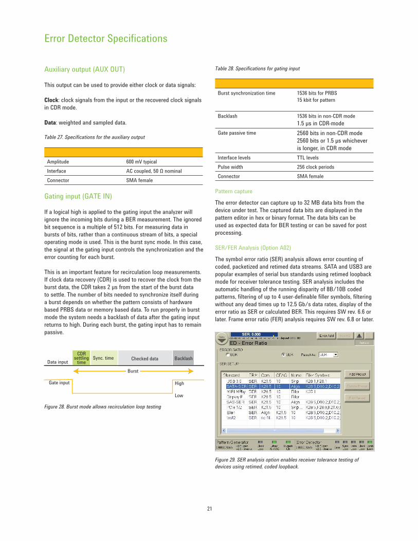
Gating input (GATE IN)
If a logical high is applied to the gating input the analyzer will
ignore the incoming bits during a BER measurement. The ignored
bit sequence is a multiple of 512 bits. For measuring data in
bursts of bits, rather than a continuous stream of bits, a special
operating mode is used. This is the burst sync mode. In this case,
the signal at the gating input controls the synchronization and the
error counting for each burst.
This is an important feature for recirculation loop measurements.
If clock data recovery (CDR) is used to recover the clock from the
burst data, the CDR takes 2 µs from the start of the burst data
to settle. The number of bits needed to synchronize itself during
a burst depends on whether the pattern consists of hardware
based PRBS data or memory based data. To run properly in burst
mode the system needs a backlash of data after the gating input
returns to high. During each burst, the gating input has to remain
passive.
Error Detector Specifi cations
Table 28. Specifi cations for gating input
Burst synchronization time 1536 bits for PRBS
15 kbit for pattern
Backlash 1536 bits in non-CDR mode
1.5 µs in CDR-mode
Gate passive time 2560 bits in non-CDR mode
2560 bits or 1.5 µs whichever
is longer, in CDR mode
Interface levels TTL levels
Pulse width 256 clock periods
Connector SMA female
Pattern capture
The error detector can capture up to 32 MB data bits from the
device under test. The captured data bits are displayed in the
pattern editor in hex or binary format. The data bits can be
used as expected data for BER testing or can be saved for post
processing.
SER/FER Analysis (Option A02)
The symbol error ratio (SER) analysis allows error counting of
coded, packetized and retimed data streams. SATA and USB3 are
popular examples of serial bus standards using retimed loopback
mode for receiver tolerance testing. SER analysis includes the
automatic handling of the running disparity of 8B/10B coded
patterns, filtering of up to 4 user-definable filler symbols, filtering
without any dead times up to 12.5 Gb/s data rates, display of the
error ratio as SER or calculated BER. This requires SW rev. 6.6 or
later. Frame error ratio (FER) analysis requires SW rev. 6.8 or later.
Figure 28. Burst mode allows recirculation loop testing
Figure 29. SER analysis option enables receiver tolerance testing of
devices using retimed, coded loopback.
Checked data BacklashCDR
settling time
Sync. time
Burst
High
Low
Gate input
Data input

22
Mainframe Characteristics
Figure 30. Rear panel view
Table 29. General mainframe characteristics
Operating temperature 5 ºC to 40 ºC (-23 to +104 ºF)
Storage temperature -40 ºC to +70 ºC (-65 to +158 ºF)
Operating humidity 95% relative humidity,
non-condensing
Storage humidity 50% relative humidity
Power requirements 100 to 240 V, ± 10%, 47 to 63 Hz,
450 VA
Physical dimensions Width: 424.5 mm (16.75 in)
Height: 221.5 mm (8.7 in)
Depth: 580.0 mm (22.9 in)
Weight (net) 26.3 kg (58.0 lb)
Weight (shipping, max) 36.3 kg (80.0 lb)
Recommended
recalibration period
1 year
Warranty period 1 year return to Agilent. See ordering
instructions for extended warranty
Remote control interfaces
Connectivity: GPIB (IEEE 488), LAN, USB 2.0.
Language: SCPI, IVI.COM. SCPI commands can be exported via
copy/paste from the utility menu/output window.
Built-in web server: provides remote GUI access and control
of J-BERT via a standard Java™ enabled web browser on your
computer.
IO libraries
Agilents IO libraries suite ships with the N4903B to help quickly
establish an error-free connection between your PC and instru-
ments regardless of the vendor.
Other interfaces
Parallel printer port, 2 x LAN, VGA output, 4 x USB 2.0, 1 x USB
1.1 (front).
Operating system
Microsoft® Windows® XP Professional
Regulatory standards
Safety:IEC 61010-1:2001 EN 61010-1:2001 CAN/CSA-C22.2
No.61010-1-04
UL 61010-1:2004
EMC: EN 61326:1997 + A1:1998 + A2:2001
IEC 61326:1997 + A1:1998 + A2:2000
Quality management: ISO 9004
Specifi cation assumptions
The specifications in this document describe the instrument’s
warranted performance.
Preliminary values are shown in italics.
Non-warranted values are described as typical.
All specifications are valid in a range from 5 °C to 40 °C ambient
temperature after a warm-up phase of 30 minutes.
If not otherwise stated, all inputs and outputs need to be termi-
nated with 50 Ω to ground.
All specifications, if not otherwise stated, are valid using the
recommended cable set N4910A (2.4 mm, 24” matched pair).
Display
8” color LCD touch screen
Data entry
• Color touch screen display, numeric keypad with up/down
arrows, dial-knob control or external key board and mouse via
USB interface
• Pattern export/import
Hard disk
For local storage of user patterns and data. An external disk is
also available for using over the USB interface.

23
Ordering Instructions
J-BERT N4903B high-performance serial BERT
Includes six 50-Ω SMA terminations, ten adaptors 3.5 mm female to 2.4 mm male, commercial calibration report and certificate (“UK6”),
getting started guide, USB cable, keyboard, mouse, and Agilent I/O library.
Table 30. Option information
J-BERT Options Description BERT with built-in and
tunable CDR N4903B
Pattern Generator
N4903B
Data rate 150 Mb/s to 12.5 Gb/s
150 Mb/s to 7 Gb/s
Extended data rate for pattern generator up
to 14.2 Gb/s
N4903B-C13
N4903B-C07
N4903B-G13
N4903B-G07
N4903B-D14 [3]
Generator capabilities PRBS and pattern on aux data output
Half-rate clock with variable duty cycle
N4903B-002
N4903B-003
Jitter tolerance options RJ, sRJ, PJ1, PJ2, SJ, BUJ injection
SSC, rSSC generation
Interference channel
(includes short cable kit N4915A-008)
Jitter tolerance compliance suite
N4903B-J10
N4903B-J11 [1]
N4903B-J20 [1]
N4903B-J12 [1]
Analyzer capabilities SER/FER analysis
Bit recovery mode
N4903B-A02
N4903B-A01—
Upgrade from N4903B Upgrade from N4903A version (factory) N4903B-UAB [2]
Upgrade options for
N4903B
Description BERT with built-in and
tunable CDR N4903BU
Pattern Generator
N4903BU
Data rate To 12.5 Gb/s (N4903B-C13/ N4903B-G13)
from 7 Gb/s (N4903B-C07/ N4903B-C13)
To 14.2 Gb/s data rate extension (factory)
N4903BU-U13
N4903BU-D14 [3]
Generator capabiltiies To PRBS and pattern on aux data output
To half-rate clock with variable duty cycle
N4903BU-U02
N4903BU-U03
Jitter tolerance options To RJ,sRJ,PJ1,PJ2,SJ,BUJ injection
To SSC, rSSC generation
To interference channel
To jitter tolerance compliance suite
N4903BU -U10
N4903BU-U11
N4903BU-J20
N4903BU-U12
Analyzer capabilities To SER/FER analysis
To bit recovery mode
To BERT from pattern generator (factory)
N4903BU-UA2
N4903BU-U01
—
—
—
N4903BU-UED
1. Only available with Option J10
2. Requires N4903A-J10/-U10 or N4903B-J10 and N4903A-CTR/-UTR or N4903B-UTR; upgrade does not include N4915A-008 short cable kit for ISI ports
3. Requires Option -G13, -C13, or -U13
Table 31. Warranty, calibration, and productivity services
Warranty 1 year return-to-Agilent warranty
1 year return-to-Agilent warranty
extended to 3 years
1 year return-to-Agilent warranty extended to 5 years
R1280: R-51 B-001-C
R1280: R-51 B-001-3C
R1280 R-51 B-001-5C
Calibration Agilent calibration upfront support plan
3 year coverage
Agilent calibration upfront support plan
5 year coverage
R1282: R-50C-011-3
R1282: R-50C-011-5
Productivity Productivity assistance, remote or on-site R1380-N49xx PS-S20 and PS-S10
24
Ordering Instructions
Table 32. Recommended accessories
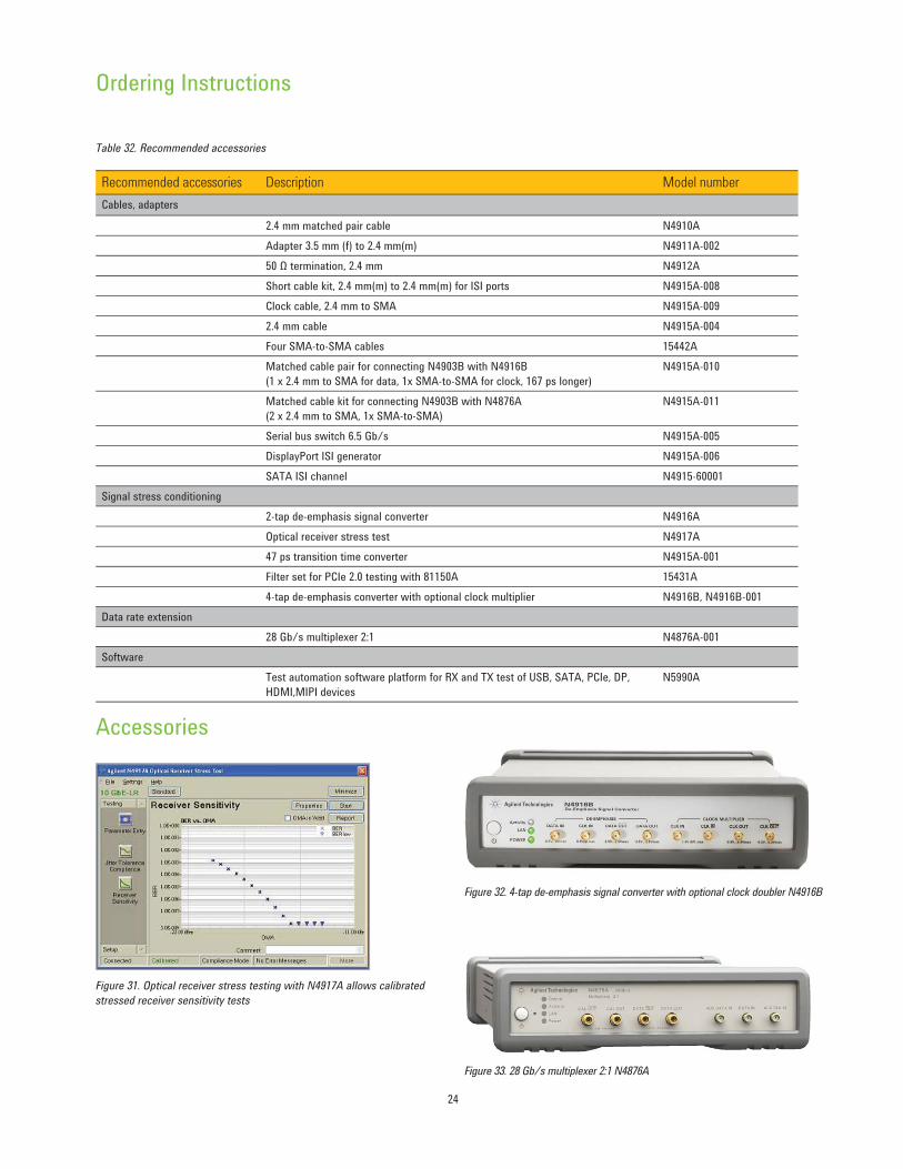
Recommended accessories Description Model number
Cables, adapters
2.4 mm matched pair cable N4910A
Adapter 3.5 mm (f) to 2.4 mm(m) N4911A-002
50 Ω termination, 2.4 mm N4912A
Short cable kit, 2.4 mm(m) to 2.4 mm(m) for ISI ports N4915A-008
Clock cable, 2.4 mm to SMA N4915A-009
2.4 mm cable N4915A-004
Four SMA-to-SMA cables 15442A
Matched cable pair for connecting N4903B with N4916B
(1 x 2.4 mm to SMA for data, 1x SMA-to-SMA for clock, 167 ps longer)
N4915A-010
Matched cable kit for connecting N4903B with N4876A
(2 x 2.4 mm to SMA, 1x SMA-to-SMA)
N4915A-011
Serial bus switch 6.5 Gb/s N4915A-005
DisplayPort ISI generator N4915A-006
SATA ISI channel N4915-60001
Signal stress conditioning
2-tap de-emphasis signal converter N4916A
Optical receiver stress test N4917A
47 ps transition time converter N4915A-001
Filter set for PCIe 2.0 testing with 81150A 15431A
4-tap de-emphasis converter with optional clock multiplier N4916B, N4916B-001
Data rate extension
28 Gb/s multiplexer 2:1 N4876A-001
Software
Test automation software platform for RX and TX test of USB, SATA, PCIe, DP,
HDMI,MIPI devices
N5990A
Accessories
Figure 31. Optical receiver stress testing with N4917A allows calibrated
stressed receiver sensitivity tests
Figure 32. 4-tap de-emphasis signal converter with optional clock doubler N4916B
Figure 33. 28 Gb/s multiplexer 2:1 N4876A
25
Title Publication number
J-BERT N4903A High-Performance Serial BERT Brochure 5989-3882EN
Bit Recovery Mode for Characterizing Idle and Framed Data Traffic Application Note 5989-3796EN
Calibrated Jitter, Jitter Tolerance Test and Jitter Laboratory with the J-BERT N4903A Application Note 5989-4967EN
Mastering Jitter Characterization with J-BERT & DCA-J Poster 5989-4823EN
PCIe® Revision 2 Receiver Jitter Tolerance Testing with J-BERT N4903B Application Note 5989-4087EN
N4906B Serial BERT 3 and 12.5 Gb/s Data sheet 5989-2406EN
Agilent Physical Layer Test Brochure 5988-9514EN
ParBERT 81250 Product Overview 5968-9188E
Infiniium DCA-J Agilent 86100C Wide-Bandwidth Oscilloscope Mainframe and Modules Data Sheet 5989-0278EN
Infiniium DSO90000 Series High-Performance Oscilloscopes Data Sheet 5989-7819EN
Fast Total Jitter Solution Application Note 5989-3151EN
N5990A Test Automation Software Platform Data Sheet 5989-5483EN
N4916A De-Emphasis Signal Converter Data Sheet 5989-6062EN
N4916B 4-Tap De-Emphasis Signal Converter Data Sheet 5990-4630EN
N4876A 28 Gb/s Multiplexer 2:1 Data Sheet 5990-5247EN
PCIe2.0 Receiver Testing Application Note 5990-3233EN
N4917A Optical Receiver Stress Test Data Sheet 5989-6315EN
Calibrating Optical Stress Signals for Characterizing 10 Gb/s Optical Transceiver Application Note 5989-8393EN
N4915A-006 DisplayPort ISI Generator Data Sheet 5989-8688EN
Agilent Method of Implementation (MOI) for DisplayPort Sink Compliance Test Application Note 5989-9147EN
Forward Clocking - Receiver Jitter Tolerance Test with J-BERT N4903B Application Note 5990-3575EN
Related Literature
Remove all doubt
Our repair and calibration services will get your equip-
ment back to you, performing like new, when promised.
You will get full value out of your Agilent equipment
through-out its lifetime. Your equipment will be ser-
viced by Agilent-trained technicians using the latest
factory calibration procedures, automated repair diag-
nostics and genuine parts. You will always have the utmost
confi dence in your measurements. For information
regarding self maintenance of this product, please
contact your Agilent offi ce.
Agilent offers a wide range of additional expert test and
measurement services for your equipment, including
initial start-up assistance, onsite education and train-
ing, as well as design, system integration, and project
management.
For more information on repair and calibration services,
go to:
www.agilent.com/fi nd/removealldoubt
Agilent Email Updates
www.agilent.com/fi nd/emailupdates
Get the latest information on the products and applications
you select.
www.agilent.comwww.agilent.com/fi nd/JBERT
“PCI-SIG” ® and the PCI SIG design marks are registered trademarks and/
or service marks of PCI-SIG ®.
Windows® and MS Windows ® are U.S. registered trademarks of
Microsoft Corporation.
Java™ is a U.S. trademark of Sun Microsystems, Inc.
For more information on Agilent Technologies’ products, applications or services, please contact your local Agilent office.
The complete list is available at:
www.agilent.com/fi nd/contactus
AmericasCanada (877) 894 4414 Latin America 305 269 7500United States (800) 829 4444
Asia Pacifi cAustralia 1 800 629 485China 800 810 0189Hong Kong 800 938 693India 1 800 112 929Japan 0120 (421) 345Korea 080 769 0800Malaysia 1 800 888 848Singapore 1 800 375 8100Taiwan 0800 047 866Thailand 1 800 226 008
Europe & Middle EastAustria 43 (0) 1 360 277 1571Belgium 32 (0) 2 404 93 40 Denmark 45 70 13 15 15Finland 358 (0) 10 855 2100France 0825 010 700* *0.125 €/minute
Germany 49 (0) 7031 464 6333 Ireland 1890 924 204Israel 972-3-9288-504/544Italy 39 02 92 60 8484Netherlands 31 (0) 20 547 2111Spain 34 (91) 631 3300Sweden 0200-88 22 55Switzerland 0800 80 53 53United Kingdom 44 (0) 118 9276201Other European Countries: www.agilent.com/fi nd/contactusRevised: October 1, 2009
Product specifications and descriptions in this document subject to change without notice.
© Agilent Technologies, Inc. 2010Printed in USA, March 22, 20105990-3217EN
Agilent Channel Partners
www.agilent.com/find/channelpartners
Get the best of both worlds: Agilent’s measurement
expertise and product breadth, combined with channel
partner convenience.