an asynchronous noc router in a 14nm finfet library...
TRANSCRIPT

An Asynchronous NoC Router in a 14nm FinFET Library: Comparison to an Industrial Synchronous Counterpart
Davide Bertozzi
University of Ferrara, Italy
Weiwei Jiang
Columbia University, USA
Steven M. Nowick
Columbia University, USA
ACM/IEEE Design, Automation and Test in Europe (DATE-17)
Gabriele Miorandi
University of Ferrara, Italy
Wayne Burleson
Advanced Micro Devices, USA
Greg Sadowski
Advanced Micro Devices, USA

Motivation for Networks-on-Chip
• CPU:
8 to 24 cores widely available - AMD 16-core Opteron 6000 series
- AMD Ryzen 4,6,8,+ cores- Intel 24-core Xeon-E7- Intel Xeon Phi – 80+ core
• GPU:
up to 2500-3500 graphics cores- AMD FirePro series:
up to 2560 GCN Stream Processors
- NVIDIA Titan X:
3584 CUDA Cores1
Future of computing is multi-core
AMD Ryzen 8-core Processor
(March 2017)

Motivation for Networks-on-Chip (Cont.)
NoC separates computation and communication
• Improves scalability- global interconnects have high latency and power consumption
(e.g. buses and point-to-point wiring)
• Increases performance/energy efficiency- share wiring resources between parallel data flows
• Facilitates design reuse- optimized IPs can simply plug in largely decrease design efforts
2

Potential Advantages of Asynchronous Design
No global clock• No clock power
less overall power than deeply clock-gated sync designs
• No clock design overhead no clock generation, distribution, skew analysis, etc.
- [Gebhardt/Stevens et al., Comparing energy and latency of asynchronous
and synchronous NoCs for embedded SoCs, NOCS-10]
Greater flexibility/modularity• Easily integrates multiple timing domains• Supports reusable components
- [Bainbridge/Furber, CHAIN: a delay-insensitive chip area interconnect, IEEE Micro-02]
Lower system latency• No per-router clock synchronization no waiting for clock
- [Sheibanyrad/Greiner et al., Multisynchronous and fully asynchronous
NoCs for GALS architectures, IEEE Design & Test of Computers-08]3
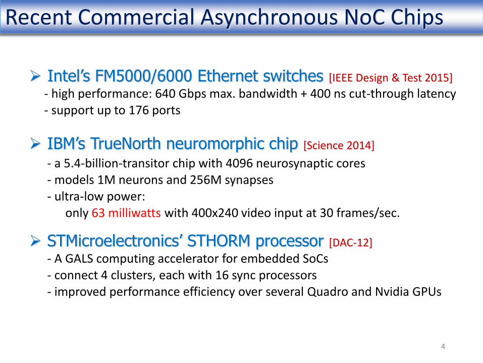
Recent Commercial Asynchronous NoC Chips
Intel’s FM5000/6000 Ethernet switches [IEEE Design & Test 2015]
- high performance: 640 Gbps max. bandwidth + 400 ns cut-through latency- support up to 176 ports
IBM’s TrueNorth neuromorphic chip [Science 2014]
- a 5.4-billion-transitor chip with 4096 neurosynaptic cores- models 1M neurons and 256M synapses- ultra-low power:
only 63 milliwatts with 400x240 video input at 30 frames/sec.
STMicroelectronics’ STHORM processor [DAC-12]
- A GALS computing accelerator for embedded SoCs- connect 4 clusters, each with 16 sync processors- improved performance efficiency over several Quadro and Nvidia GPUs
4
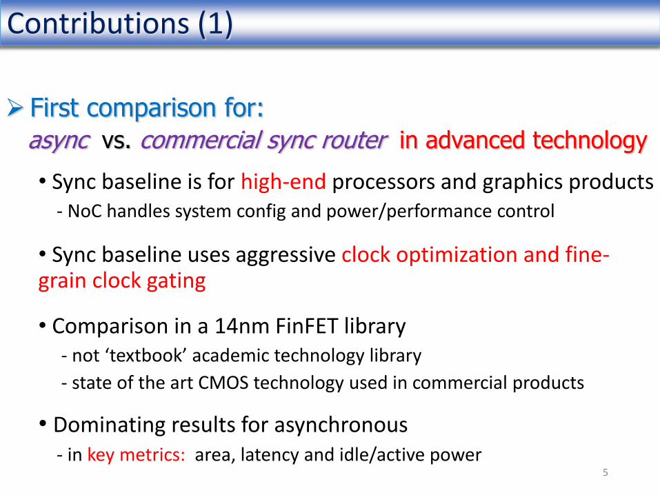
Contributions (1)
First comparison for:
async vs. commercial sync router in advanced technology
• Sync baseline is for high-end processors and graphics products- NoC handles system config and power/performance control
• Sync baseline uses aggressive clock optimization and fine-grain clock gating
• Comparison in a 14nm FinFET library- not ‘textbook’ academic technology library
- state of the art CMOS technology used in commercial products
• Dominating results for asynchronous- in key metrics: area, latency and idle/active power
5

Contributions (2)
Implementation and validation at pre- and post-layout
• results presented only for pre-layout (confidentiality reasons)
Industrial tools used in async design and validation
• Functional validation tool (using Synopsys environment)
- wrapper added for async design for sync environment re-use
- used for both pre- and post-layout implementations
• Place & Route tool (using AMD’s internal tool environment)
- largely manual synthesis + automated P&R
- expect automated logic synthesis can be included with reasonable efforts
6
(e.g.,an existing solution is proposed in [Ghiribaldi/Bertozzi/Nowick DATE-13])

Contributions (3)
A novel async end-to-end credit-based Virtual Channel control scheme
• Key idea = lazy credit-update approach- credit-increments are queued and no immediate update
- credit updated only with a credit-decrement
- fewer backward credit synchronization to upstream router
• Potential increased throughput
• VC is required for practical industrial usage- many existing async NoCs do not include VCs
• Not the focus of this presentation (see paper for details)
7

Proposed Asynchronous Node Structure
8
Switch 0
Switch 1
Wes
t In
terf
ace
East
In
terf
ace
North Interface
South Interface
Loc
al Inte
rfac
e
Request Plane
West Channel
Router for
Request Plane
Request Plane
South ChannelResponse Plane
South Channel
Request Plane
East Channel
Response Plane
East Channel
Request Plane
North Channel
Response Plane
North ChannelLocal
Terminal
Response Plane
West Channel
Router for
Response Plane
Request Plane Router
Response Plane Router
Two identical and uncorrelated planes
Follows AMD sync baseline router architecture
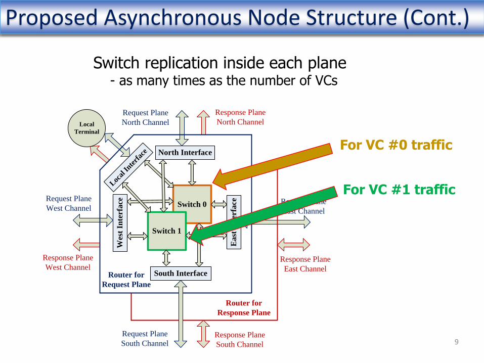
Proposed Asynchronous Node Structure (Cont.)
9
Switch 0
Switch 1
Wes
t In
terf
ace
East
In
terf
ace
North Interface
South Interface
Loc
al Inte
rfac
e
Request Plane
West Channel
Router for
Request Plane
Request Plane
South ChannelResponse Plane
South Channel
Request Plane
East Channel
Response Plane
East Channel
Request Plane
North Channel
Response Plane
North ChannelLocal
Terminal
Response Plane
West Channel
Router for
Response Plane
For VC #0 traffic
For VC #1 traffic
Switch replication inside each plane- as many times as the number of VCs

Node Operation
10
Example: data from west input -> east output
Datain Dataout
Switch 0
Switch 1
Wes
t In
terf
ace
East
In
terf
ace
North Interface
South Interface
Loc
al Inte
rfac
e
Request Plane
West Channel
Router for
Request Plane
Request Plane
South ChannelResponse Plane
South Channel
Request Plane
East Channel
Response Plane
East Channel
Request Plane
North Channel
Response Plane
North ChannelLocal
Terminal
Response Plane
West Channel
Router for
Response Plane
De-mux data to a switch Merge data from 2 VCs
Data traverses the switch {
1
2
3
Header sets up the pathBody/tail flits follow the pre-set up path

New Components in the Async Router
11
Two new components added on previous DATE-13 async router
Switch 0
Switch 1
Wes
t In
terf
ace
East
In
terf
ace
North Interface
South Interface
Loc
al Inte
rfac
e
Request Plane
West Channel
Router for
Request Plane
Request Plane
South ChannelResponse Plane
South Channel
Request Plane
East Channel
Response Plane
East Channel
Request Plane
North Channel
Response Plane
North ChannelLocal
Terminal
Response Plane
West Channel
Router for
Response Plane
Input Interface
Output Interface
Switch 0
Switch 1
Req
ues
t P
lane
Eas
t C
han
nel
Input interface:
New high-performance Input buffer
[Ghiribaldi/Bertozzi/Nowick DATE-13]
Identical switches; new components in ‘router interfaces’
Output interface:
New VC control

Input Buffer Circular FIFO: Forward Latency
12
Forward latency: 2 x D→Q latch delay + XOR2 + XOR4
Written-in data can be immediately read out(not aligned to clk cycle: much faster than a sync circular FIFO)
Default-open single D-latch register
Default-open single D-latch register + XOR2

Input Buffer Circular FIFO: Storage Element
13
Each async storage element = single level-sensitive D-latch register
- Each latch register has full storage capacity
- Half area/power cost as a typical Flip-Flop storage in sync
key source for performance/area/power benefits 13

Output Interface Design: Proposed VC Control
14
Blocks or allows output traffic for a particular VC
(See details in the paper)
Updates downstream credits only every time a flit is sent out
Mutex
Mutex
Input Ctl0
Mutex
Input Ctl1
Full
Detector0
Timer 0
mutex_req0
mutex_req1
zerowins
forced_clk0
full0
full
0_val
id
Full
Detector1
Timer 1
onewins
forced_clk1
full1
full1
_valid
ED Q
L1 ED Q
L2
ED Q
L6E
D QL7
ED Q
L5
L3
D Q
E
L4
D Q
E
Ackin
Reqout
Credit_increment0
Credit_increment1
Ackout1
Ackout0
Reqin0
Reqin1
Data
Mu
x
R S
Q
sel
Datain0
Datain1
E
D Q
DataReg
Dataout
Q
_
Two
da
ta in
pu
t c
ha
nn
els
: e
ac
h f
rom
a
diffe
ren
t V
C a
nd
co
rre
spo
nd
ing
sw
itc
h (
OP
M)
Da
ta o
utp
ut
ch
an
ne
l:
to t
he
ou
tpu
t lin
k
VC c ontrols:
from the output link

Design Validation Tool
15
Pre- or Post-layout netlist
Synchronize async I/O data
to a given clockAsync Router
Design
Wrapper
Standard Sync Simulator
Re-used standard sync I/Os and benchmarks
(Ideal wrapper,
not considering metastability)

Design Flow and Place & Route Tool
Expect further synthesis automation can be included with reasonable effort
16
Manual Synthesis
Automated P&R
Timing
violations?
Manual Timing
Correction
Yes
No
Final Layout
Manually add inverter chainsManually derive gate netlist
Standard sync P&R with ‘don’t touch’ everything
- An async logic synthesis solution was proposed in [Ghiribaldi/Bertozzi/Nowick DATE-13]

Actual Layout for Asynchronous Router
17
Local channel pins North channels pins
Wes
t ch
ann
el p
ins
East
ch
ann
el p
ins
South channel pins
Router config.:- double-plane router- 5 port + 2 VCs

Experimental Results: Overview
AMD commercial sync router vs. proposed async router
• Identical router configuration for both routers
- 5-port + 2 VCs
- buffer depth = 7 for each VC
• Pre-layout results only (for confidentiality reasons)
- post-layout comparisons expected to be similar for small designs
• One testing benchmark: activating all switch ports
- evenly distributed traffic from all inputs to all outputs
- sufficient for initial router-level results
• Testing corner: 14nm FinFET library (0.65V, TT)
Additional projected results for more complex routers
• 7-port router with 2 VCs for 3D stacking
• 5-port router with 8 VCs more realistic VC configuration
18

Basic comparison: 5-port router with 2 VCs
Comparison for 5-port router with 2 VCs
19
Asynchronous router dominates in area, latency and power
55% lower 28% lower 88% lower 58% lower
Sync routerAsync router

Projected Results for More Complex Routers
Absolute area and power costs are noticeably increased- due to higher radix or more VCs
Relative asynchronous benefits are largely maintained
20
Comparison for 5-port router with 8 VCs
Comparison for 7-port router with 2 VCs
Sync 5-port 2 VCsAsync 5-port 2 VCs
Sync 7-port 2 VCsAsync 7-port 2 VCs
Sync 5-port 8 VCsAsync 5-port 8 VCs
47% lower
16% lower
85% lower
51% lower
47% lower
28% lower
85% lower
51% lower

Conclusions
First “async vs. commercial sync router” in advanced library• Sync router optimized for high-end products with fine-grain clock-gating
• Comparison in 14nm FinFET library
Industrial tools for async design and validation• Design validation tool: sync testing environments are largely re-used
• Manual synthesis + automated P&R
- synthesis automation can be further included with some effort
• Shows opportunity for industrial asynchronous designs
• Some remaining tool challenges for full automation
A novel async end-to-end credit-based VC control approach• Lazy credit-update approach potential higher throughput
Results: async router shows significant benefits• In key metrics: area, latency and power
21