automatic layout generation using silicon ensemble
TRANSCRIPT

Automatic Layout GenerationUsing Silicon Ensemble
CheeWe [email protected]
This document can be downloaded from http://www-mtl.mit.edu/research/icsystems/research/presentations.html

Outline
• Overview of Design FlowFrom High-level description to IC Layout
• Tutorial Example• Setting up Tools• Where to find more information

Overview of Design Flow
High-levelDescription
SynopsysDesignAnalyzer
VerilogNetlist
VerilogNetlist
CadenceSilicon Ensemble
CadenceVirtuoso
ICLayout
We’ll come back to this picture to talk about setting upthe libraries for these tools.
Logic Synthesis
Place and Route

Outline
• Overview of Design FlowFrom High-level description to IC Layout
• Tutorial Example• Setting up Tools• Where to find more information

Tutorial Example
• 4 bit adder in VHDLlibrary IEEE;use IEEE.std_logic_1164.all;use IEEE.std_logic_signed.all;
entity example isport(A: in std_logic_vector(3 downto 0);
B: in std_logic_vector(3 downto 0); Y: out std_logic_vector(3 downto 0));
end example;
architecture behavior of example isbeginY<=A+B;end;

Step 1:Design Analyzer
• At the prompt (assuming the path and license environment variable is set), typedesign_analyzer
• Read in the VHDL file by using the File Read menu
• Open the command window by using the Setup Command Window menu
• At the command window prompt, typecompile

Design Analyzer
Ascend/descendhierarchy
Synthesizedschematic
Analysis tools
Standard Cells
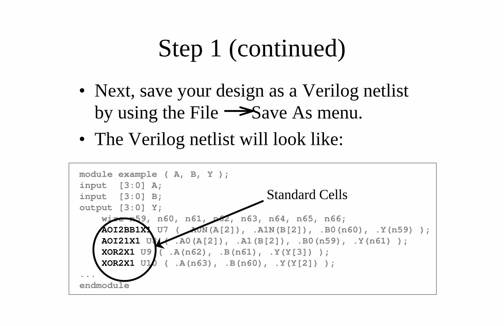
Step 1 (continued)
• Next, save your design as a Verilog netlist by using the File Save As menu.
• The Verilog netlist will look like:
module example ( A, B, Y );input [3:0] A;input [3:0] B;output [3:0] Y;
wire n59, n60, n61, n62, n63, n64, n65, n66;AOI2BB1X1 U7 ( .A0N(A[2]), .A1N(B[2]), .B0(n60), .Y(n59) );AOI21X1 U8 ( .A0(A[2]), .A1(B[2]), .B0(n59), .Y(n61) );XOR2X1 U9 ( .A(n62), .B(n61), .Y(Y[3]) );XOR2X1 U10 ( .A(n63), .B(n60), .Y(Y[2]) );
...endmodule
Standard Cells

Step 2: Silicon Ensemble
• Run silicon ensemble by typing seultra
Menu bar for all functions
Console
CommandLine
Zoom,pan, display,etc

Silicon Ensemble (Import LEF)• Import “.lef” files that
tells SE where the pins of each cell are located:File Import LEF
These are provided by the cell-library provider, e.g. Artisan Components
Anantha, Charlie, and Harry’s groups can look at/vader/cheewe/artisan/current/aci/sc/

Step 2 (continued)• Import Verilog netlist
from logic synthesis– Need to import a
module declaration of all the standard-cells in Verilog as well.
– Be sure to specify the name of the top module, e.g. “example”

Step 2 (continued)• Floorplan Initialize Floorplan menu
IO To Core Distance:Region for Vdd and Gnd rings
Select “Flip Every Other Row

Silicon Ensemble (after Floorplan)
Rows for cellplacement
Space for Vdd and Gnd Rings

Step 2 (continued)• Place Place IOs • Place Place Cells

Silicon Ensemble (after placement)
Placed IO Pins
Unused Slots
Placed cells with Vdd and Gnd Rails

Step 2 (continued)• Add filler cells: • Place Filler Cells
Add
FILL1 is a standard-cell with no transistors
You can deselect all the options

Step 2 (continued)• Add power and ground rings:
– Route Plan Power and Click “Add Rings”
– Route Connect Rings”
Ring Width & position

Silicon Ensemble (w/ rings and filler cells)
Filler Cells
Vdd and Gnd Rings

Step 2 (continued)• Routing: Route WRoute

Silicon Ensemble (placed & routed)
Routing
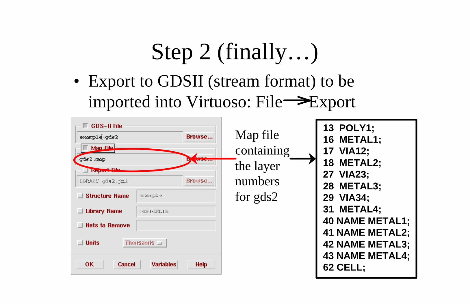
Step 2 (finally…)• Export to GDSII (stream format) to be
imported into Virtuoso: File Export13 POLY1; 16 METAL1; 17 VIA12; 18 METAL2; 27 VIA23; 28 METAL3; 29 VIA34; 31 METAL4; 40 NAME METAL1;41 NAME METAL2;42 NAME METAL3;43 NAME METAL4;62 CELL;
Map file containing the layer numbers for gds2

Step 3: Cadence Virtuoso• Run Design Framework by typing icfb
Menu to run Library Manager and to import GDSII from Silicon Ensemble

Step 3 (continued)• Import GDSII file from Silicon Ensemble:
File Import-Stream
Files from the foundry, e.g. TSMC
User-Defined Data
Anantha, Charlie, and Harry’s groups can look at/vader/cheewe/tsmc/Virtuoso

Virtuoso Layout• Tools Library Manager Open Layout

Outline
• Overview of Design FlowFrom High-level description to IC Layout
• Tutorial Example• Setting up Tools• Where to find more information
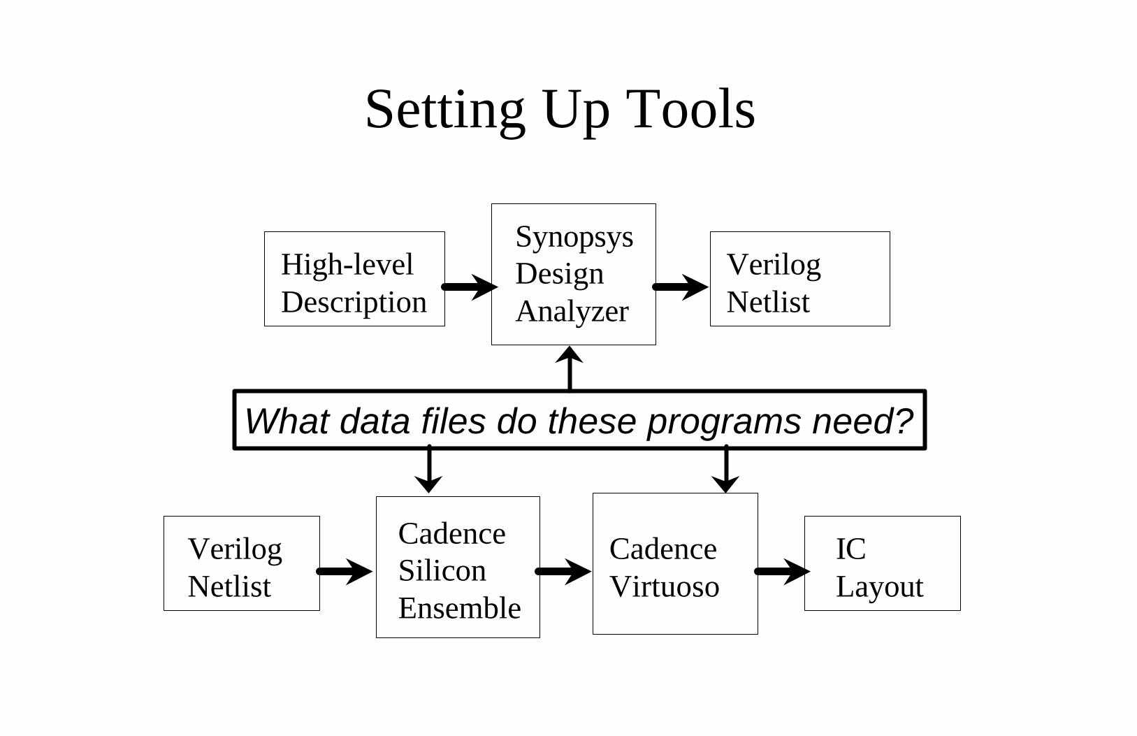
Setting Up Tools
High-levelDescription
SynopsysDesignAnalyzer
VerilogNetlist
VerilogNetlist
CadenceSilicon Ensemble
CadenceVirtuoso
ICLayout
What data files do these programs need?

Design Analyzer
• Needs– DesignWare (comes with Design Analyzer)– Standard-cell “back-end views”
• These files are usually named *.db, *.sldb, *.lib

Settting up Design Analyzer
• Need a .synopsys_dc.setup in the directory you run design analyzer.
...search_path= search_path + ${synopsys_root}/libraries/syn+ ${synopsys_root}/dw/sim_ver]+"/u/vader/cheewe/artisan/current/aci/sc/synopsys"+ "/u/vader/cheewe/artisan/current/aci/sc/vhdl"target_library=typical.dbsymbol_library=typical.dbsynthetic_library=dw_foundation.sldb# additions from DesignWare Foundation Quick Referencelink_library={typical.db, dw_foundation.sldb}synlib_wait_for_design_license={"DesignWare-Foundation"}...
Standard-cell Library DesignWare

Setting up Silicon Ensemble
• Need a se.ini in the directory Silicon Ensemble is launched:
# from /u/vader/cheewe/artisan/aci/sc/lef/README# Silicon Ensemble floorplan variables - required for TSMC .18set v plan.rgrid.M1offset 560 ;set v plan.rgrid.M2offset 660 ;set v plan.rgrid.M3offset 560 ;
set v groute.Allow.OffGrid.PinAccess false ;set v froute.Allow.OffGrid.PinAccess false ;set v froute.Avoid.OffGrid.Blockage true ;set v froute.Build.OffGrid.SPins false ;
# so that pins are labeled with [] which is compatible with # spice and verilogSET VAR INPUT.VERILOG.BUS.DELIM "[]" ;

Setting up Design Framework
• Need to create a library that has the “front-end” layout views of all the standard-cells, and the display.drf file:– Import the GDSII layout views from the cell
provider into a new library, like previously described.
– Set up the display resource, like you would with any technology.

Cadence Display Resource
• LSW: File Display Resource EditorFile Load

Outline
• Overview of Design FlowFrom High-level description to IC Layout
• Tutorial Example• Setting up Tools• Where to find more information

Where to find more information?
• Synopsys SOLD (Anantha Group)acroread/usr/synopsys/current/doc/online/synth/dctut/toc.pdf
• Cadence Openbook: (MTL Users)openbook -f /amd/mtlcad/cadence/DES4.3/doc/ASICpnr/silref/silrefTOC.obk