bapatla engineering college ece department …srinivasaraot.webs.com/ec-252 de lab.pdf ·...
TRANSCRIPT
BAPATLA ENGINEERING COLLEGE ECE DEPARTMENT
BAPATLA ENGINEERING COLLEGE ECE DEPARTMENT
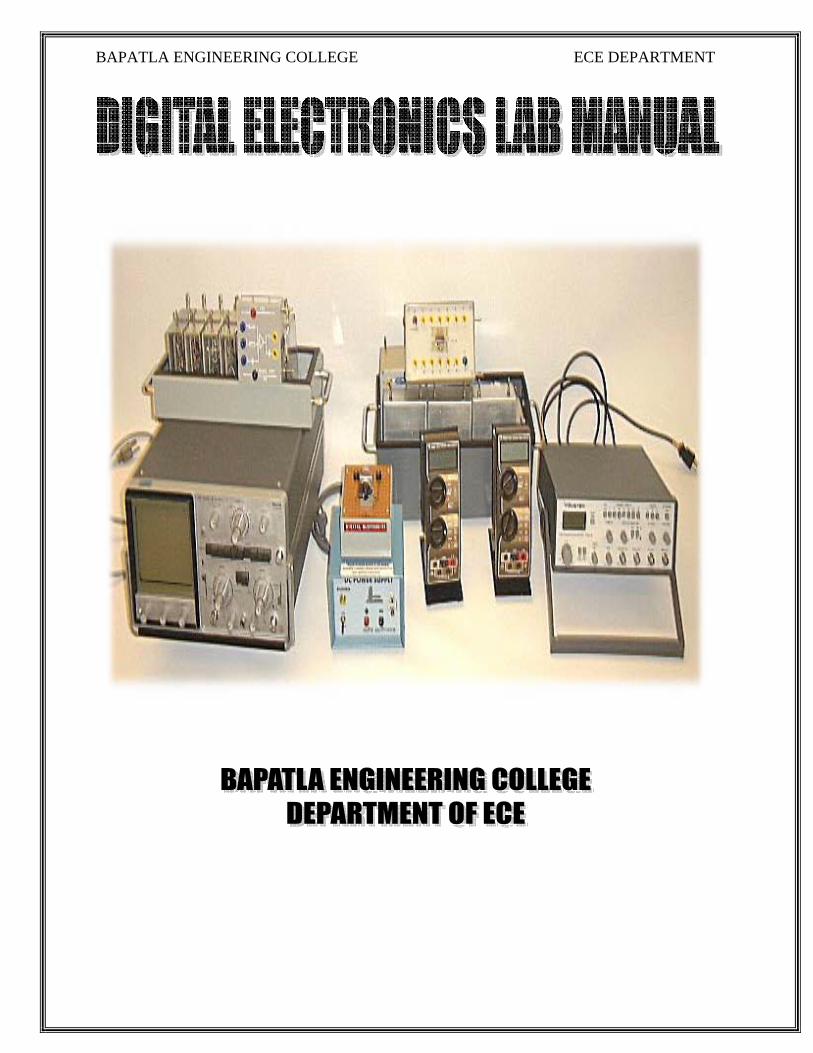
DIGITAL ELECTRONICS LAB MANUAL
FOR
2/4 B.Tech (ECE)
COURSE CODE: EC-252
PREPARED BY
P.SURENDRA KUMAR M.TECH, Lecturer
D.SWETHA M.TECH, Lecturer
T Srinivasa Rao M.TECH, Lecturer
Ch.Madhavi , Lab Assistant
ECE DEPARTMENT
2009-2010
BAPATLA ENGINEERING COLLEGE ECE DEPARTMENT
LIST OF EXPERIMENTS
S.No Name of the Experiment Page No
1. Realization of Gates using Discrete Components......................................................................01
2. Realization of Gates using Universal Building Block(NAND only)………………………….04
3. Design of Combinational Logic Circuits like Half-Adder, Full-Adder, Half- Subtractor and
Full-Subtractor………………………………………………………………………………...07
4. Verification of 4-Bit Magnitude Comparator…………………………………………………10
5. Design of Decoders like BCD-Decimal decoder……………………………………………...15
6. Applications of IC Parallel Adder(1’s and 2’s compliment addition)………………………..17
7. Design of Code Converters (Binary to Gray)…………………………………………………19
8. Design of Multiplexers/De Multiplexers ……………………………………………………..21
9. Verification of Truth Table of Flip-Flops using Gates………………………………………..23
10. Design of Shift register (To verify Serial to Parallel, Parallel to Serial ,Serial to Serial and
Parallel to Parallel Converters) using Flip-Flops……………………………………...……..26
11. Design of Ring & Johnson Counters using Flip-Flops………………………………………30
12. Conversion of Flip-Flops (JK-T, JK-D)……………………………………………...………32
13. Design of Binary/Decade Counter……………………………………………………...……34
14. Design Asynchronous Counter, Mod Counter, Up Counter, Down Counter and Up/Down
Counter……………………………………………………………………………………….36
15. Design Synchronous Counter, Mod Counter, Up Counter, Down Counter and Up/Down
Counter……………………………………………………………………………………….39
BAPATLA ENGINEERING COLLEGE ECE DEPARTMENT
The Laboratory Notebook:
Each student must have their own laboratory notebook. All pre-lab exercises and laboratory reports are to be entered into your notebook.
Your notebook must be clearly labelled on the cover with the following information:
Module: Digital Electronics - Name: Register no: 4 Class: Lab Partner Name:

BAPATLA ENGINEERING COLLEGE ECE DEPARTMENT
STUDENTS GUIDELINES
There are 3 hours allocated to a laboratory session in Digital Electronics. It is a necessary part of the course at which attendance is compulsory.
Here are some guidelines to help you perform the experiments and to submit the reports:
1. Read all instructions carefully and carry them all out.
2. Ask a demonstrator if you are unsure of anything.
3. Record actual results (comment on them if they are unexpected!)
4. Write up full and suitable conclusions for each experiment.
5. If you have any doubt about the safety of any procedure, contact the demonstrator beforehand.
6. THINK about what you are doing!
BAPATLA ENGINEERING COLLEGE ECE DEPARTMENT
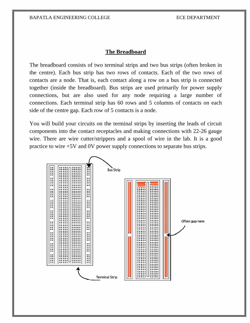
The Breadboard
The breadboard consists of two terminal strips and two bus strips (often broken inthe centre). Each bus strip has two rows of contacts. Each of the two rows ofcontacts are a node. That is, each contact along a row on a bus strip is connectedtogether (inside the breadboard). Bus strips are used primarily for power supplyconnections, but are also used for any node requiring a large number ofconnections. Each terminal strip has 60 rows and 5 columns of contacts on each side of the centre gap. Each row of 5 contacts is a node.
You will build your circuits on the terminal strips by inserting the leads of circuitcomponents into the contact receptacles and making connections with 22-26 gauge wire. There are wire cutter/strippers and a spool of wire in the lab. It is a goodpractice to wire +5V and 0V power supply connections to separate bus strips.

BAPATLA ENGINEERING COLLEGE ECE DEPARTMENT
Fig 1. The breadboard. The lines indicate connected holes.
The 5V supply MUST NOT BE EXCEEDED since this will damage the ICs (Integrated circuits) used during the experiments. Incorrect connection of power tothe ICs could result in them exploding or becoming very hot - with the possible serious injury occurring to the people working on the experiment! Ensure that the power supply polarity and all components and connections are correctbefore switching on power .
Building the Circuit:
Throughout these experiments we will use TTL chips to build circuits. The stepsfor wiring a circuit should be completed in the order described below:
1. Turn the power (Trainer Kit) off before you build anything! 2. Make sure the power is off before you build anything! 3. Connect the +5V and ground (GND) leads of the power supply to the
power and ground bus strips on your breadboard. 4. Plug the chips you will be using into the breadboard. Point all the chips in
the same direction with pin 1 at the upper-left corner. (Pin 1 is often identified by a dot or a notch next to it on the chip package)
5. Connect +5V and GND pins of each chip to the power and ground bus strips on the breadboard.
6. Select a connection on your schematic and place a piece of hook-up wire between corresponding pins of the chips on your breadboard. It is better tomake the short connections before the longer ones. Mark each connection on your schematic as you go, so as not to try to make the same connectionagain at a later stage.
7. Get one of your group members to check the connections, before you turn the power on.
8. If an error is made and is not spotted before you turn the power on. Turn the power off immediately before you begin to rewire the circuit.
9. At the end of the laboratory session, collect you hook-up wires, chips and all equipment and return them to the demonstrator.
10. Tidy the area that you were working in and leave it in the same condition as it was before you started.
BAPATLA ENGINEERING COLLEGE ECE DEPARTMENT
Common Causes of Problems:
1. Not connecting the ground and/or power pins for all chips. 2. Not turning on the power supply before checking the operation of the
circuit. 3. Leaving out wires. 4. Plugging wires into the wrong holes. 5. Driving a single gate input with the outputs of two or more gates 6. Modifying the circuit with the power on.
In all experiments, you will be expected to obtain all instruments, leads,components at the start of the experiment and return them to their proper place afteryou have finished the experiment. Please inform the demonstrator or technician ifyou locate faulty equipment. If you damage a chip, inform a demonstrator, don't putit back in the box of chips for somebody else to use.
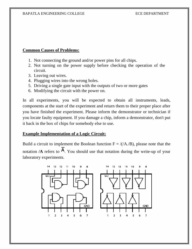
Example Implementation of a Logic Circuit:
Build a circuit to implement the Boolean function F = /(/A./B), please note that the
notation /A refers to . You should use that notation during the write-up of your laboratory experiments.
BAPATLA ENGINEERING COLLEGE ECE DEPARTMENT
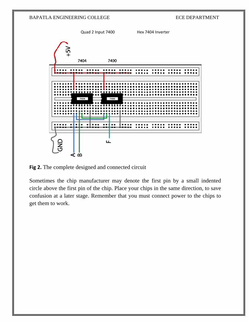
Quad 2 Input 7400 Hex 7404 Inverter
Fig 2. The complete designed and connected circuit
Sometimes the chip manufacturer may denote the first pin by a small indentedcircle above the first pin of the chip. Place your chips in the same direction, to save confusion at a later stage. Remember that you must connect power to the chips toget them to work.
BAPATLA ENGINEERING COLLEGE ECE DEPARTMENT
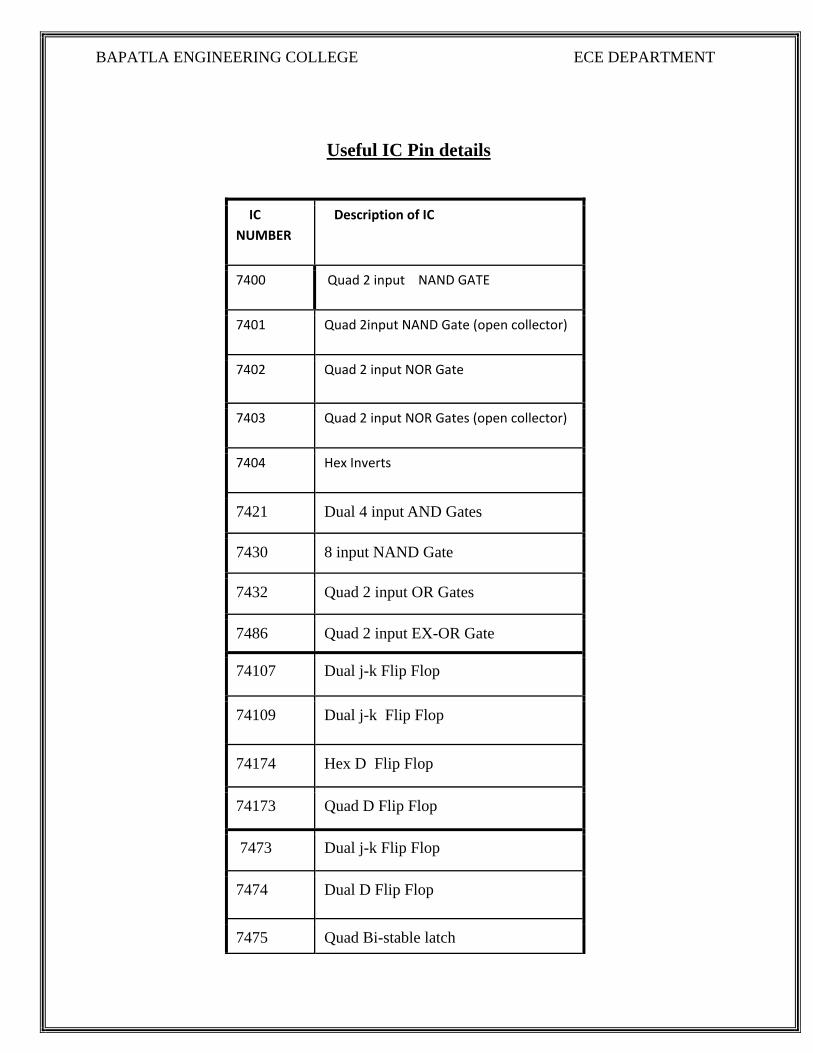
Useful IC Pin details
IC NUMBER
Description of IC
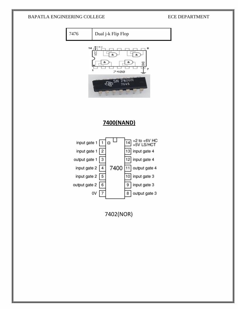
7400 Quad 2 input NAND GATE
7401 Quad 2input NAND Gate (open collector)
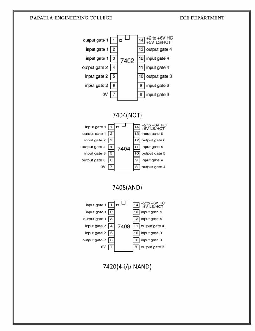
7402 Quad 2 input NOR Gate
7403 Quad 2 input NOR Gates (open collector)
7404 Hex Inverts
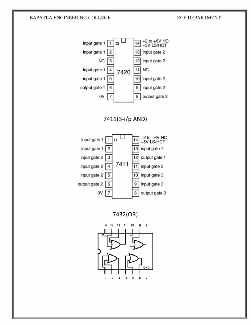
7421 Dual 4 input AND Gates
7430 8 input NAND Gate
7432 Quad 2 input OR Gates
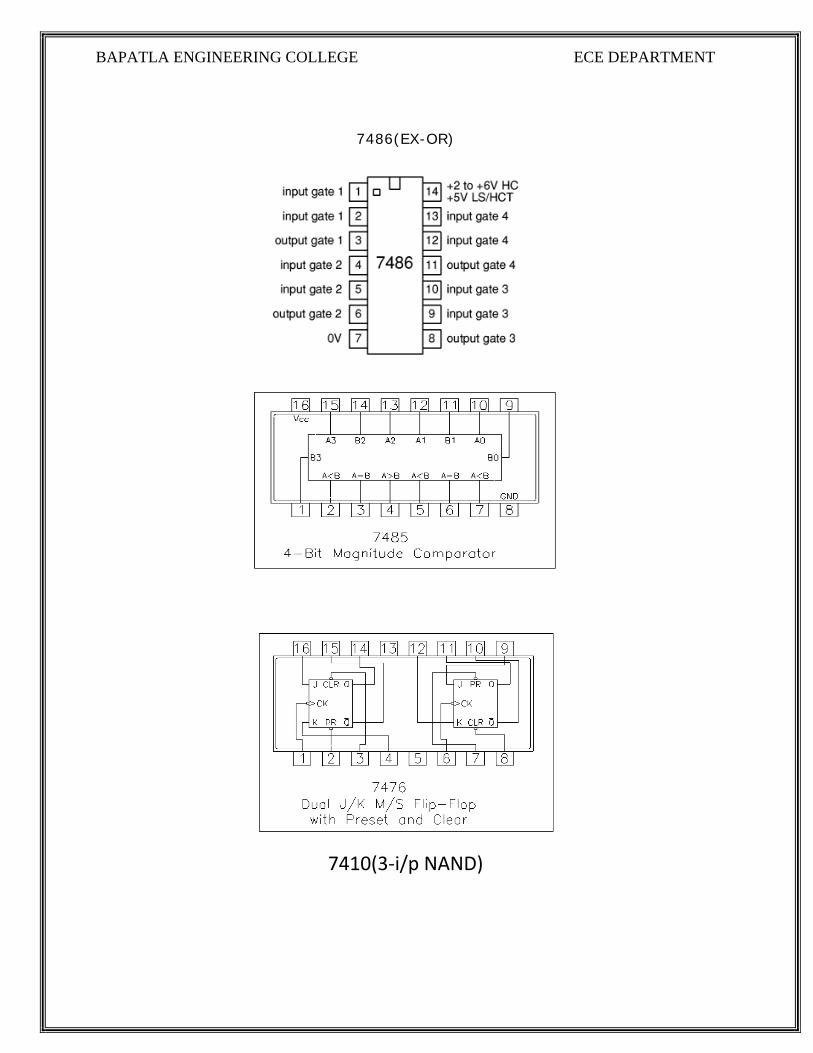
7486 Quad 2 input EX-OR Gate
74107 Dual j-k Flip Flop
74109 Dual j-k Flip Flop
74174 Hex D Flip Flop
74173 Quad D Flip Flop
7473 Dual j-k Flip Flop
7474 Dual D Flip Flop
7475 Quad Bi-stable latch
BAPATLA ENGINEERING COLLEGE ECE DEPARTMENT
7476 Dual j-k Flip Flop
7400(NAND)
7402(NOR)
BAPATLA ENGINEERING COLLEGE ECE DEPARTMENT
7404(NOT)
7408(AND)
7420(4‐i/p NAND)
BAPATLA ENGINEERING COLLEGE ECE DEPARTMENT
7411(3‐i/p AND)
7432(OR)
BAPATLA ENGINEERING COLLEGE ECE DEPARTMENT
7486(EX-OR)
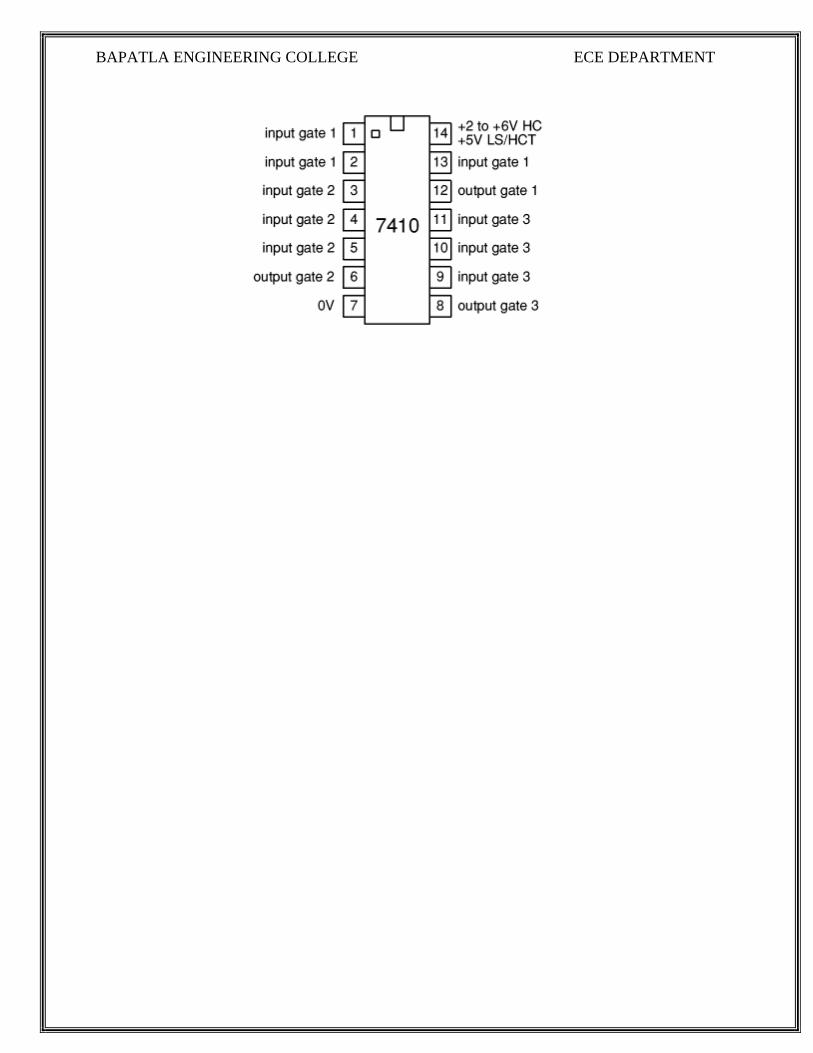
7410(3‐i/p NAND)
BAPATLA ENGINEERING COLLEGE ECE DEPARTMENT
BAPATLA ENGINEERING COLLEGE ECE DEPARTMENT
1
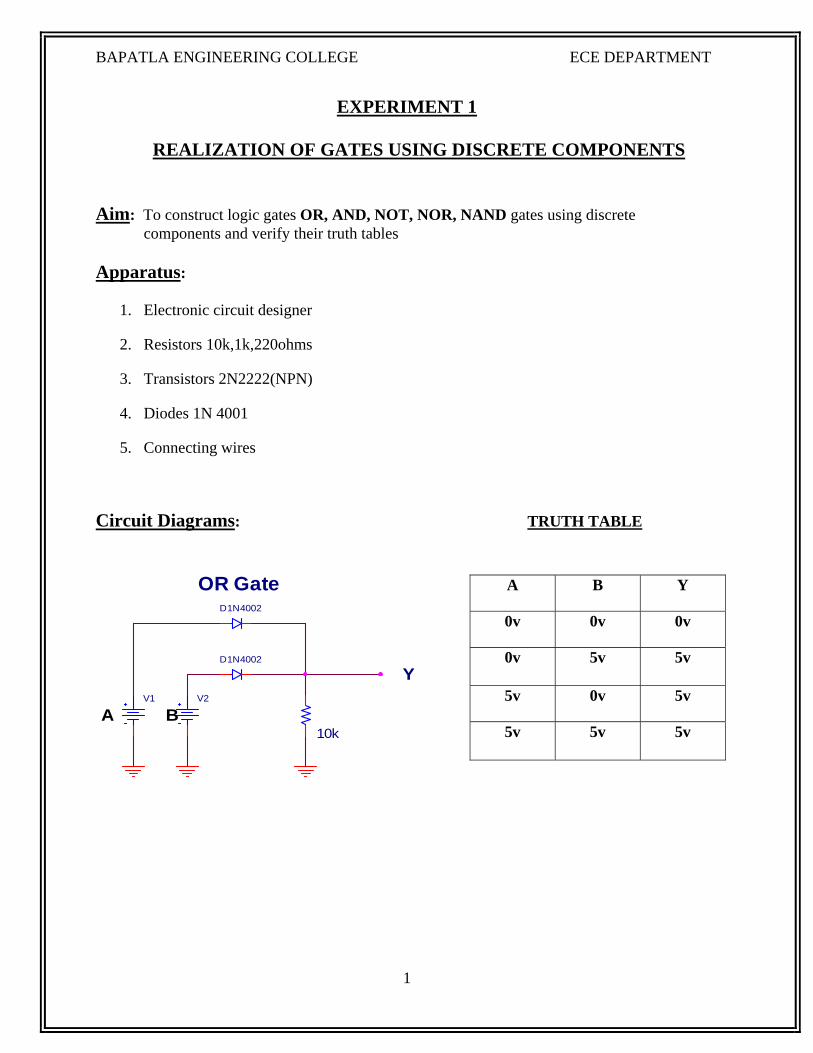
EXPERIMENT 1
REALIZATION OF GATES USING DISCRETE COMPONENTS
Aim: To construct logic gates OR, AND, NOT, NOR, NAND gates using discrete components and verify their truth tables
Apparatus:
1. Electronic circuit designer
2. Resistors 10k,1k,220ohms
3. Transistors 2N2222(NPN)
4. Diodes 1N 4001
5. Connecting wires
Circuit Diagrams: TRUTH TABLE
A B Y
0v 0v 0v
0v 5v 5v
5v 0v 5v
5v 5v 5v
V1
A
V2
B
YD1N4002
OR GateD1N4002
10k

BAPATLA ENGINEERING COLLEGE ECE DEPARTMENT
2
A B Y
0v 0v 0v
0v 5v 0v
5v 0v 0v
5v 5v 5v
A Y
0v 5v
5v 0v
A B Y
0v 0v 5v
0v 5v 0v
5v 0v 0v
5v 5v 0v
+ 5 V
A
V2
B
YD1N4002
AND Gate
D1N4002
1k
NOT Gate
Y
1k
A
+ 5 V
10k
Q2N2222
+ 5 V
A
B
10 kY
D1N4002
NOR Gate
D1N4002
Q2N2222
1k
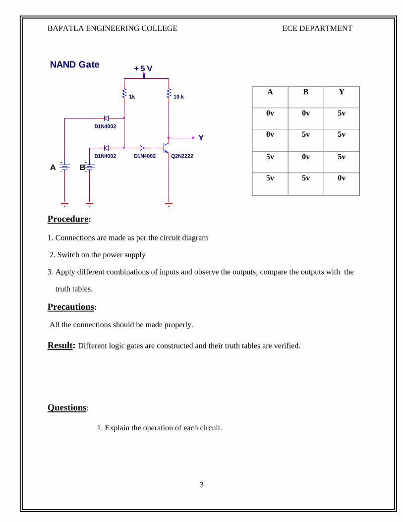
BAPATLA ENGINEERING COLLEGE ECE DEPARTMENT
3
+ 5 V
A
B
1k 10 k
Y
D1N4002
NAND Gate
D1N4002
Q2N2222D1N4002
Procedure:
1. Connections are made as per the circuit diagram
2. Switch on the power supply
3. Apply different combinations of inputs and observe the outputs; compare the outputs with the
truth tables.
Precautions:
All the connections should be made properly. Result: Different logic gates are constructed and their truth tables are verified. Questions: 1. Explain the operation of each circuit.
A B Y
0v 0v 5v
0v 5v 5v
5v 0v 5v
5v 5v 0v
BAPATLA ENGINEERING COLLEGE ECE DEPARTMENT
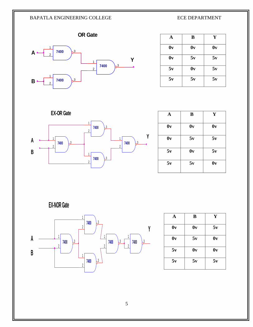
4
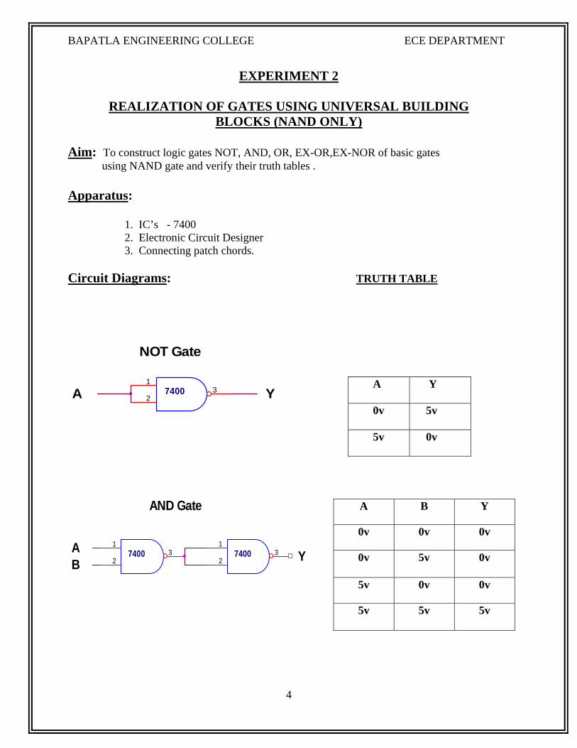
EXPERIMENT 2
REALIZATION OF GATES USING UNIVERSAL BUILDING BLOCKS (NAND ONLY)
Aim: To construct logic gates NOT, AND, OR, EX-OR,EX-NOR of basic gates
using NAND gate and verify their truth tables . Apparatus:
1. IC’s - 7400 2. Electronic Circuit Designer 3. Connecting patch chords. Circuit Diagrams: TRUTH TABLE
74001
23 Y
NOT Gate
A
A Y
0v 5v
5v 0v
A B Y
0v 0v 0v
0v 5v 0v
5v 0v 0v
5v 5v 5v
AB Y
AND Gate
74001
237400
1
23
BAPATLA ENGINEERING COLLEGE ECE DEPARTMENT
5
A
B 74001
23
Y
OR Gate
74001
23
74001
23
A B Y
0v 0v 0v
0v 5v 5v
5v 0v 5v
5v 5v 5v
A B Y
0v 0v 0v
0v 5v 5v
5v 0v 5v
5v 5v 0v
A B Y
0v 0v 5v
0v 5v 0v
5v 0v 0v
5v 5v 5v
A
B7400
1
23
Y
EX-OR Gate
74001
23 7400
1
23
74001
23
A
B7400
1
23
Y
EX-NOR Gate
74001
23 7400
1
23 7400
1
23
74001
23

BAPATLA ENGINEERING COLLEGE ECE DEPARTMENT
6
Procedure: 1. Connect the logic gates as shown in the diagrams. 2. Feed the logic signals 0 or 1 from the logic input switches in different combinations at the inputs A & B. 3. Monitor the output using logic output LED indicators. 4. Repeat steps 1 to 3 for NOT, AND, OR, EX – OR & EX-NOR operations. and compare the outputs with the truth tables.
Precautions:
1. All the connections should be made properly.
2. IC should not be reversed.
Result: Different logic gates are constructed using NAND gates and their truth tables are verified. Questions: 1. Why NAND & NOR gates are called universal gates? 2. Realize the EX – OR gates using minimum number of NAND gates? 3. Give the truth table for EX-NOR (EX-OR+NOT) and realize using NAND gates . 4. Realize the given logic function using NAND gates?
f = ABC + ABC + ABC

BAPATLA ENGINEERING COLLEGE ECE DEPARTMENT
7
EXPERIMENT 3
DESIGN OF COMBINATIONAL LOGIC CIRCUITS Aim: - To design and construct Half-adder, Full-adder, Half-subtractor, Full- subtractor Apparatus: -
1. IC’s - 7486, 7432, 7408, 7400 2. Electronic Circuit Designer 3. Connecting patch chords.
Circuit Diagram:- TRUTH TABLE
A B S C
0 0 0 0
0 1 1 0
1 0 1 0
1 1 0 1
A B C N-1 S C
0 0 0 0 0
0 0 1 1 0
0 1 0 1 0
0 1 1 0 1
1 0 0 1 0
1 0 1 0 1
1 1 0 0 1
1 1 1 1 1
Half Adder:
SXY
C74081
23
74861
23
74081
23
Full Adder:
S7486
1
23
74321
23
X
Z
Y
C
74081
23
74861
23
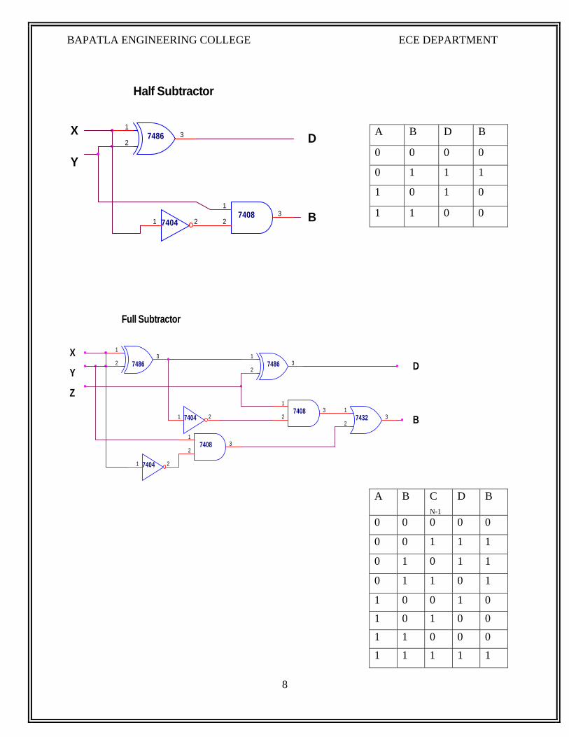
BAPATLA ENGINEERING COLLEGE ECE DEPARTMENT
8
74861
23
Half Subtractor
74041 2 B
X
Y
D
74081
23
7486
1
23
Full Subtractor
74041 2 74321
23
74041 2
B
X
Y D74861
23
74081
23
74081
23
Z
A B D B
0 0 0 0
0 1 1 1
1 0 1 0
1 1 0 0
A B C N-1
D B
0 0 0 0 0
0 0 1 1 1
0 1 0 1 1
0 1 1 0 1
1 0 0 1 0
1 0 1 0 0
1 1 0 0 0
1 1 1 1 1

BAPATLA ENGINEERING COLLEGE ECE DEPARTMENT
9
Procedure: - 1. Verify the gates. 2. Make the connections as per the circuit diagram. 3. Switch on VCC and apply various combinations of input according to truth table. 4. Note down the output readings for half/full adder and half/full subtractor, Sum/difference and the carry/borrow bit for different combinations of inputs verify their truth tables. Precautions:
1. All the connections should be made properly.
2. IC should not be reversed.
Result: Combinational logic circuits like Half-adder, Full-adder, Half-subtractor, Full- subtractor are constructed and truth tables are verified. Questions:
1. Describe the difference between half-adder and full-adder. 2. Describe the difference between half -subtractor and full-
subtractor.
BAPATLA ENGINEERING COLLEGE ECE DEPARTMENT
10
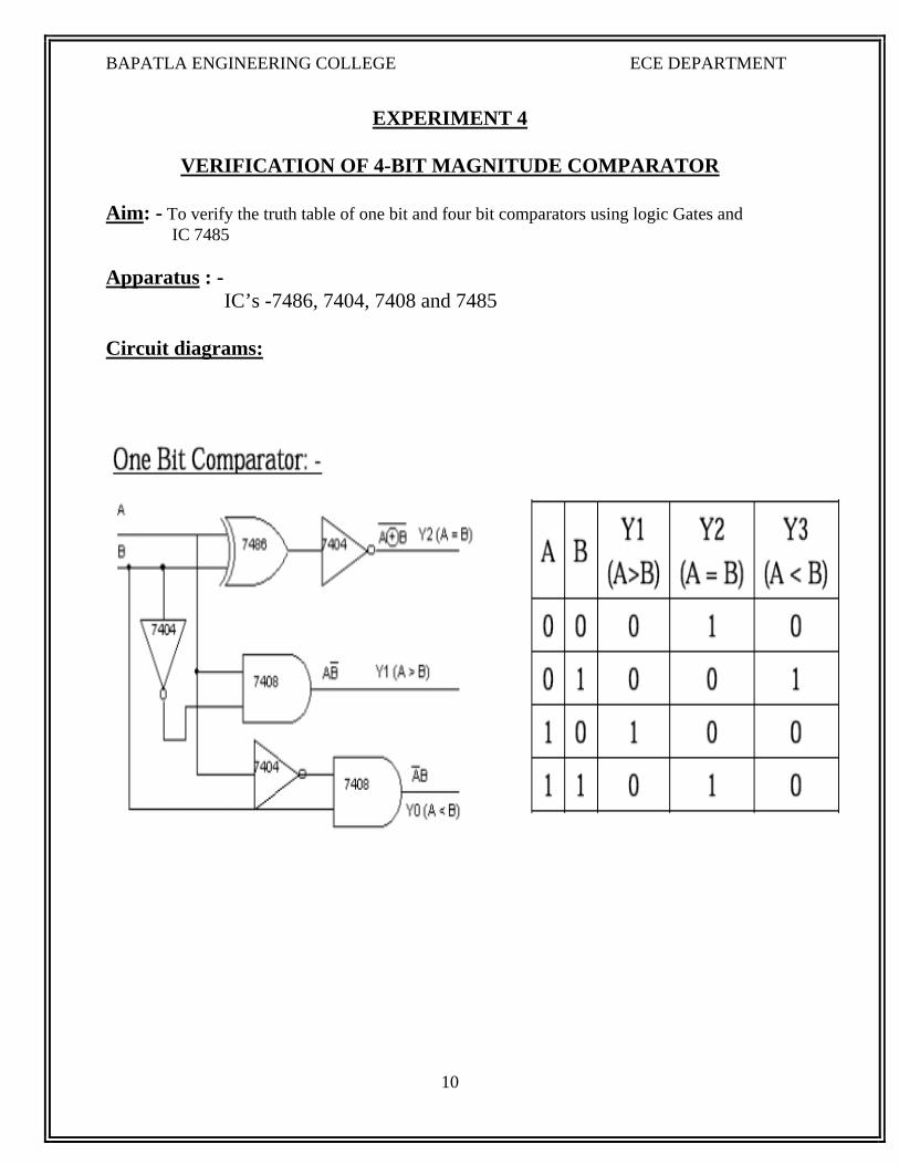
EXPERIMENT 4
VERIFICATION OF 4-BIT MAGNITUDE COMPARATOR
Aim: - To verify the truth table of one bit and four bit comparators using logic Gates and IC 7485 Apparatus : - IC’s -7486, 7404, 7408 and 7485 Circuit diagrams:
BAPATLA ENGINEERING COLLEGE ECE DEPARTMENT
11
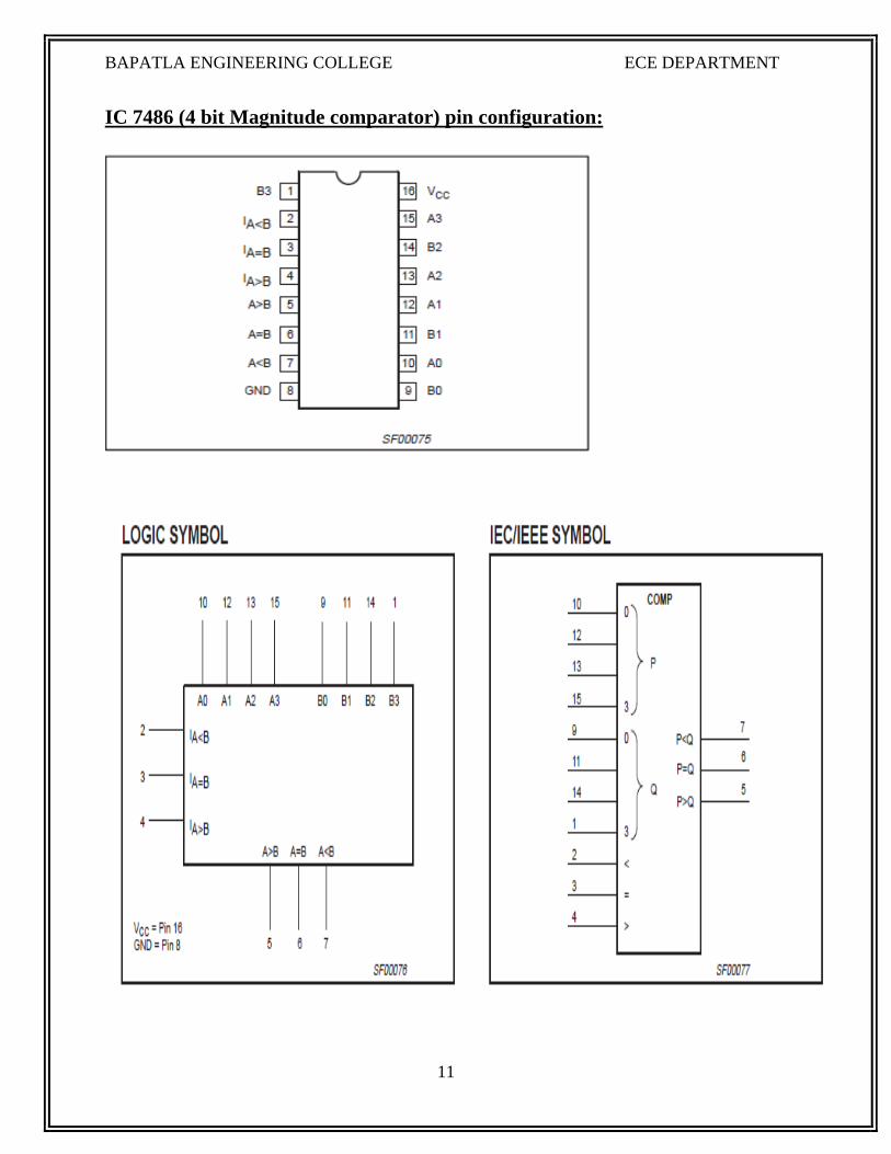
IC 7486 (4 bit Magnitude comparator) pin configuration:
BAPATLA ENGINEERING COLLEGE ECE DEPARTMENT
12
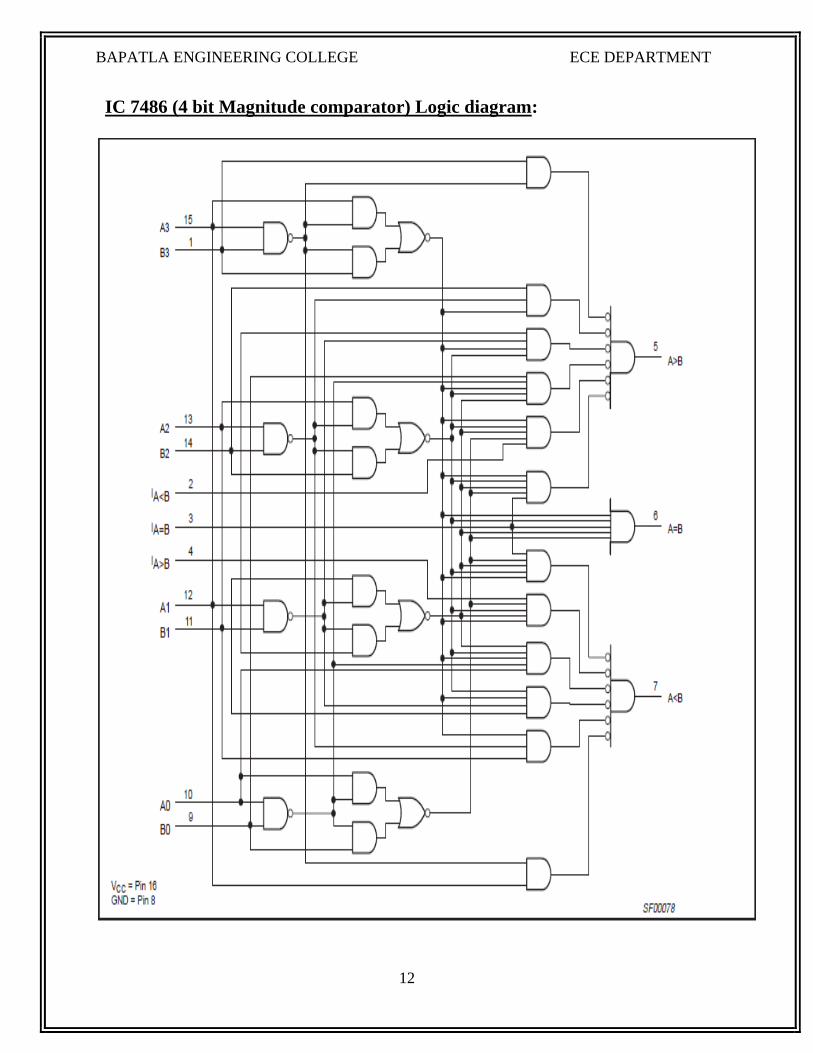
IC 7486 (4 bit Magnitude comparator) Logic diagram:
BAPATLA ENGINEERING COLLEGE ECE DEPARTMENT
13
BAPATLA ENGINEERING COLLEGE ECE DEPARTMENT
14
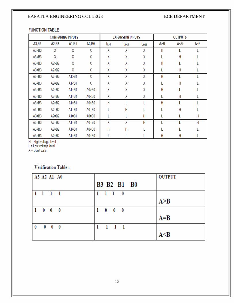
DESCRIPTION: The 74F85 is a 4-bit magnitude comparator that can be expanded to almost any length. It compares two 4-bit binary, BCD, or other monotonic codes and presents the three possible magnitude results at the outputs. The 4-bit inputs are weighted (A0–A3) and (B0–B3) where A3 and B3 are the most significant bits. The operation of the74F85 is described in the Function Table, showing all possible logic conditions. The upper part of the table describes the normal operation under all conditions that will occur in a single device or in a series expansion scheme. In the upper part of the table the three outputs are mutually exclusive. In the lower part of the table, the outputs reflect the feed-forward conditions that exist in the parallel expansion scheme.
The expansion inputs IA>B, and IA=B and IA<B are the least significant bit positions. When used for series expansion, the A>B, A=B and A<B outputs of the lease significant word are connected to the corresponding IA>B, IA=B and IA<B inputs of the next higher stage. Stages can be added in this manner to any length, but a propagation delay penalty of about 15ns is added with each additional stage. For proper operation, the expansion inputs of the least significant word should be tied as follows: IA>B = Low, Procedure: - 1. Connect the circuit as shown in fig. Feed the 4-bit binary words A0, A1, A2 , A3 and B0, B1 , B2 , B3 from the logic input switches. 2. Pin 3 of IC 7485 should be at logic 1 to enable compare operation. 3. Observe the output A>B, A=B , and A<B on logic indicators. The outputs must be 1 or 0 respectively. 4. Repeat the steps 1 ,2 and 3 for various inputs A0 ,A1 , A2 , A3 and B0 , B1 , B2 , B3 and observe the outputs at A>B , A=B and A<B . Precautions:
1. All the connections should be made properly. 2. IC should not be reversed. Result: The truth tables of one bit and four bit magnitude comparators are verified. Questions :- 1. What is Comparator? 2. What are the applications of Comparator? 3. Which logic is used as 1 bit comparator?
BAPATLA ENGINEERING COLLEGE ECE DEPARTMENT
15
EXPERIMENT 5
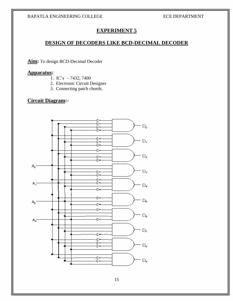
DESIGN OF DECODERS LIKE BCD-DECIMAL DECODER
Aim: To design BCD-Decimal Decoder Apparatus:
1. IC’s - 7432, 7400 2. Electronic Circuit Designer 3. Connecting patch chords. Circuit Diagram:-
BAPATLA ENGINEERING COLLEGE ECE DEPARTMENT
16
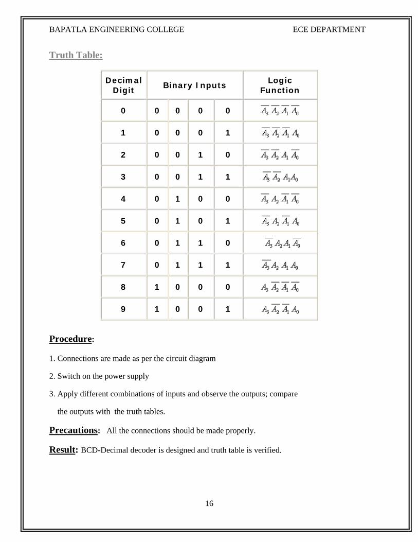
Truth Table:
Decimal Digit Binary Inputs Logic
Function
0 0 0 0 0
1 0 0 0 1
2 0 0 1 0
3 0 0 1 1
4 0 1 0 0
5 0 1 0 1
6 0 1 1 0
7 0 1 1 1
8 1 0 0 0
9 1 0 0 1
Procedure:
1. Connections are made as per the circuit diagram
2. Switch on the power supply
3. Apply different combinations of inputs and observe the outputs; compare
the outputs with the truth tables.
Precautions: All the connections should be made properly.
Result: BCD-Decimal decoder is designed and truth table is verified.
BAPATLA ENGINEERING COLLEGE ECE DEPARTMENT
17
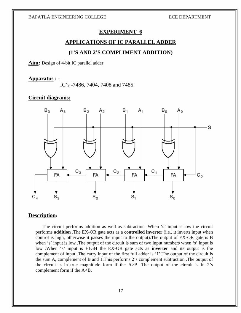
EXPERIMENT 6
APPLICATIONS OF IC PARALLEL ADDER
(1’S AND 2’S COMPLIMENT ADDITION)
Aim: Design of 4-bit IC parallel adder
Apparatus : - IC’s -7486, 7404, 7408 and 7485 Circuit diagrams:
Description:
The circuit performs addition as well as subtraction .When ‘s’ input is low the circuit performs addition .The EX-OR gate acts as a controlled inverter (i.e., it inverts input when control is high, otherwise it passes the input to the output).The output of EX-OR gate is B when ‘s’ input is low .The output of the circuit is sum of two input numbers when ‘s’ input is low .When ‘s’ input is HIGH the EX-OR gate acts as inverter and its output is the complement of input .The carry input of the first full adder is ‘1’.The output of the circuit is the sum A, complement of B and 1.This performs 2’s complement subtraction .The output of the circuit is in true magnitude form if the A>B .The output of the circuit is in 2’s complement form if the A<B.

BAPATLA ENGINEERING COLLEGE ECE DEPARTMENT
18
Procedure:
1. Connections are made as per the circuit diagram
2. Switch on the power supply
3. Apply different combinations of inputs and observe the outputs.
Precautions: All the connections should be made properly.
Result: 4-bit IC parallel adder is designed and 1’s &2’s complement addition is performed
BAPATLA ENGINEERING COLLEGE ECE DEPARTMENT
19
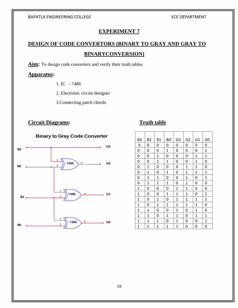
EXPERIMENT 7
DESIGN OF CODE CONVERTORS (BINARY TO GRAY AND GRAY TO
BINARYCONVERSION)
Aim: To design code converters and verify their truth tables
Apparatus:
1. IC - 7486
2. Electronic circuit designer
3.Connecting patch chords
Circuit Diagrams: Truth table
B3
B2
B1
BO
G3
G2
G1
G0
0 0 0 0 0 0 0 0 0 0 0 1 0 0 0 1 0 0 1 0 0 0 1 1 0 0 1 1 0 0 1 0 0 1 0 0 0 1 1 0 0 1 0 1 0 1 1 1 0 1 1 0 0 1 0 1 0 1 1 1 0 1 0 0 1 0 0 0 1 1 0 0 1 0 0 1 1 1 0 1 1 0 1 0 1 1 1 1 1 0 1 1 1 1 1 0 1 1 0 0 1 0 1 0 1 1 0 1 1 0 1 1 1 1 1 0 1 0 0 1 1 1 1 1 1 0 0 0
G3
G1
G0
74861
23
B1
74861
23
G2B2
B3
74861
23
B0
Binary to Gray Code Converter
BAPATLA ENGINEERING COLLEGE ECE DEPARTMENT
20
Procedure: -
1. The circuit connections are made as shown in fig.
2. Pin (14) is connected to +Vcc and Pin (7) to ground.
3 In the case of binary to gray conversion, the inputs B0, B1, B2 and B3 are given at
respective pins and outputs G0, G1, G2, G3 are taken for all the 16 combinations of the input.
4. In the case of gray to binary conversion, the inputs G0, G1, G2 and G3 are given at respective
Pins and outputs B0, B1, B2, and B3 are taken for all the 16 combinations of inputs.
5. The values of the outputs are tabulated.
Result: code converters are designed and their truth tables are verified.
Precautions: All the connections should be made properly.
Questions:
1. Convert binary 100100 to gray code.
G3
G2
G1
GO
B3
B2
B1
B0
0 0 0 0 0 0 0 0 0 0 0 1 0 0 0 1 0 0 1 0 0 0 1 1 0 0 1 1 0 0 1 0 0 1 0 0 0 1 1 1 0 1 0 1 0 1 1 0 0 1 1 0 0 1 0 0 0 1 1 1 0 1 0 1 1 0 0 0 1 1 1 1 1 0 0 1 1 1 1 0 1 0 1 0 1 1 0 0 1 0 1 1 1 1 0 1 1 1 0 0 1 0 0 0 1 1 0 1 1 0 0 1 1 1 1 0 1 0 1 1 1 1 1 1 1 0 1 0
G3
G1
G0
74861
23
B1
74861
23
G2 B2
B3
74861
23
B0
Gray to Binary Code Converter
BAPATLA ENGINEERING COLLEGE ECE DEPARTMENT
21
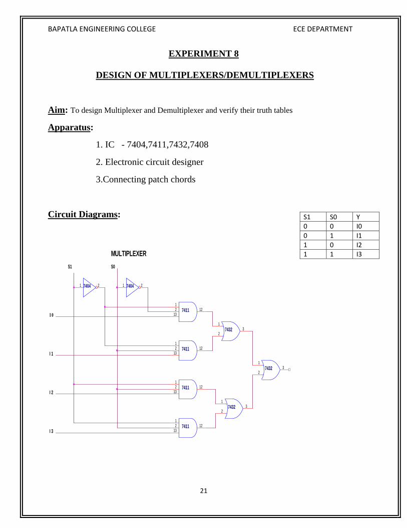
EXPERIMENT 8
DESIGN OF MULTIPLEXERS/DEMULTIPLEXERS
Aim: To design Multiplexer and Demultiplexer and verify their truth tables
Apparatus:
1. IC - 7404,7411,7432,7408
2. Electronic circuit designer
3.Connecting patch chords
Circuit Diagrams:
741112
1312
74041 2
I 2
S0
MULTIPLEXER
I 3
I 17411
12
1312
74321
23
74041 2
74321
23
741112
1312
I 0
741112
1312
S1
74321
23
S1 S0 Y 0 0 I0 0 1 I1 1 0 I2 1 1 I3
BAPATLA ENGINEERING COLLEGE ECE DEPARTMENT
22
Procedure:
1. Connections are made as per the circuit diagram
2. Switch on the power supply
3. Apply different combinations of inputs and observe the outputs; compare
the outputs with the truth tables.
Precautions: All the connections should be made properly.
Result: Multiplexer and Demultiplexer are constructed and the truth tables are verified
Questions:
1. What is the difference between multiplexer and decoder
A B Y3 Y2 Y1 Y0
0 0 0 0 0 1
0 1 0 0 1 0
1 0 0 1 0 0
1 1 1 0 0 0
7408
1
23
7408
1
23
74081
23
74041 2
Y1
Y3
74041 2
7408
1
23 Y0
Demultiplexer
BA
Y2
BAPATLA ENGINEERING COLLEGE ECE DEPARTMENT
23
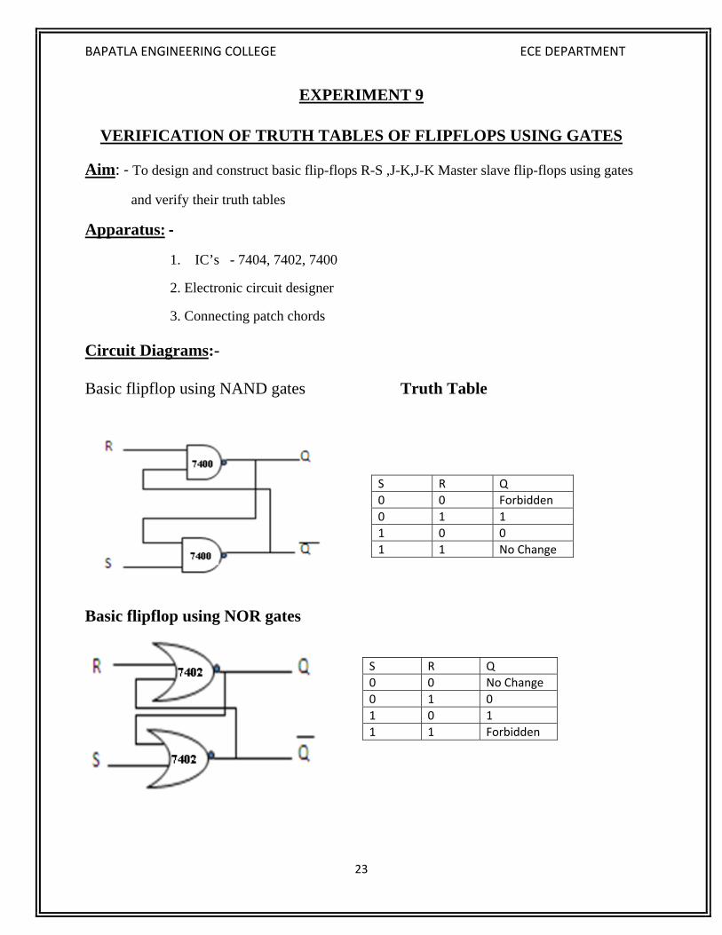
EXPERIMENT 9
VERIFICATION OF TRUTH TABLES OF FLIPFLOPS USING GATES
Aim: ‐ To design and construct basic flip-flops R-S ,J-K,J-K Master slave flip-flops using gates
and verify their truth tables
Apparatus: ‐
1. IC’s - 7404, 7402, 7400
2. Electronic circuit designer
3. Connecting patch chords
Circuit Diagrams:-
Basic flipflop using NAND gates Truth Table
Basic flipflop using NOR gates
S R Q 0 0 Forbidden 0 1 1 1 0 0 1 1 No Change
S R Q 0 0 No Change 0 1 0 1 0 1 1 1 Forbidden
BAPATLA ENGINEERING COLLEGE ECE DEPARTMENT
24
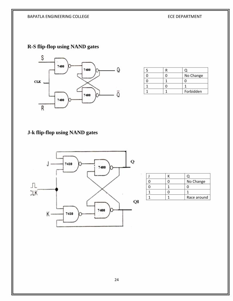
R-S flip-flop using NAND gates
J-k flip-flop using NAND gates
S R Q 0 0 No Change 0 1 0 1 0 1 1 1 Forbidden
J K Q 0 0 No Change 0 1 0 1 0 1 1 1 Race around
BAPATLA ENGINEERING COLLEGE ECE DEPARTMENT
25
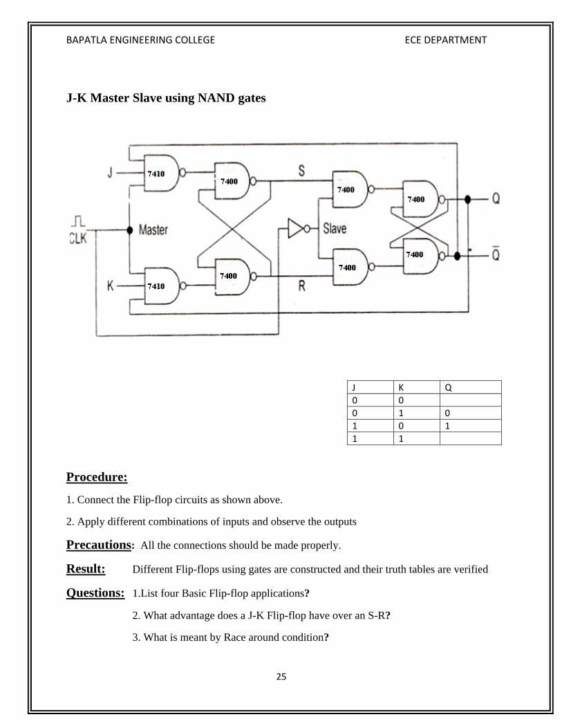
J-K Master Slave using NAND gates
Procedure:
1. Connect the Flip-flop circuits as shown above.
2. Apply different combinations of inputs and observe the outputs
Precautions: All the connections should be made properly.
Result: Different Flip-flops using gates are constructed and their truth tables are verified
Questions: 1.List four Basic Flip-flop applications?
2. What advantage does a J-K Flip-flop have over an S-R?
3. What is meant by Race around condition?
J K Q 0 0 0 1 0 1 0 1 1 1
BAPATLA ENGINEERING COLLEGE ECE DEPARTMENT
26
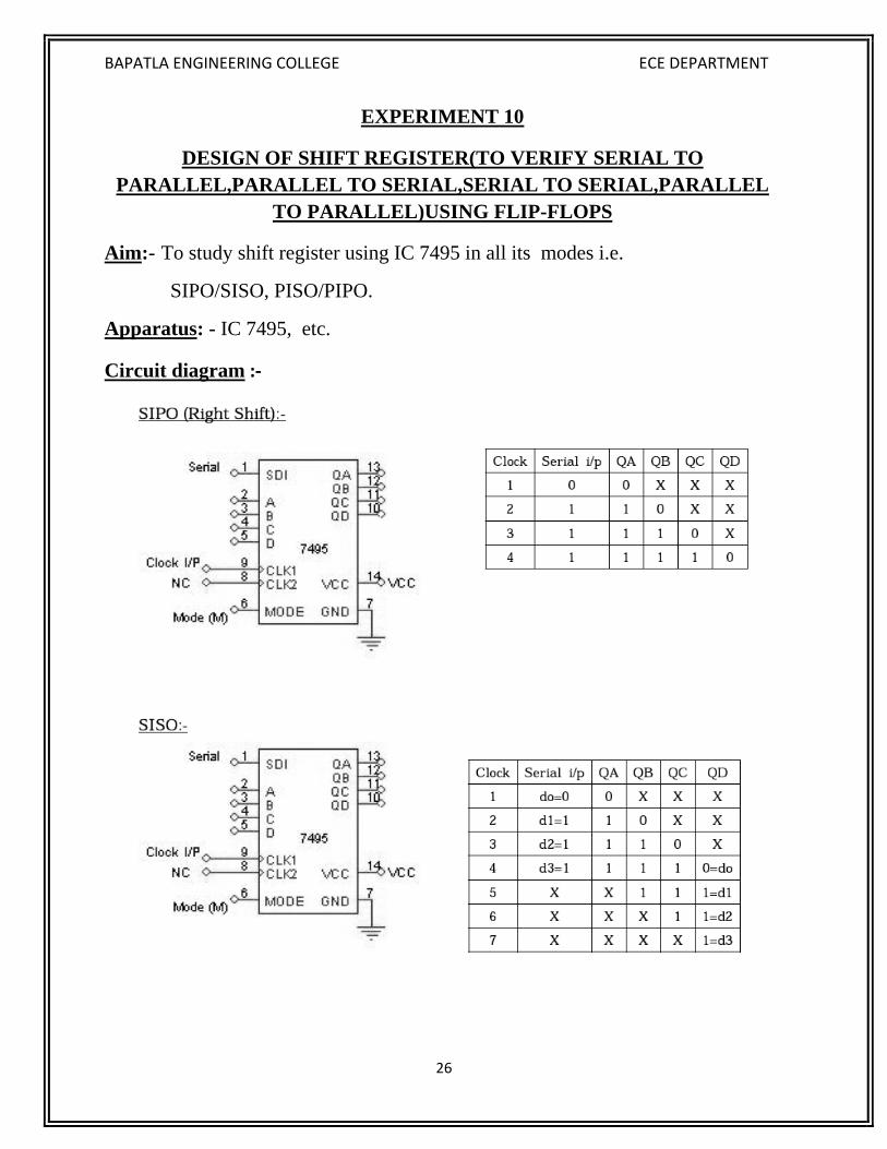
EXPERIMENT 10
DESIGN OF SHIFT REGISTER(TO VERIFY SERIAL TO PARALLEL,PARALLEL TO SERIAL,SERIAL TO SERIAL,PARALLEL
TO PARALLEL)USING FLIP-FLOPS
Aim:- To study shift register using IC 7495 in all its modes i.e.
SIPO/SISO, PISO/PIPO. Apparatus: - IC 7495, etc.
Circuit diagram :‐
BAPATLA ENGINEERING COLLEGE ECE DEPARTMENT
27
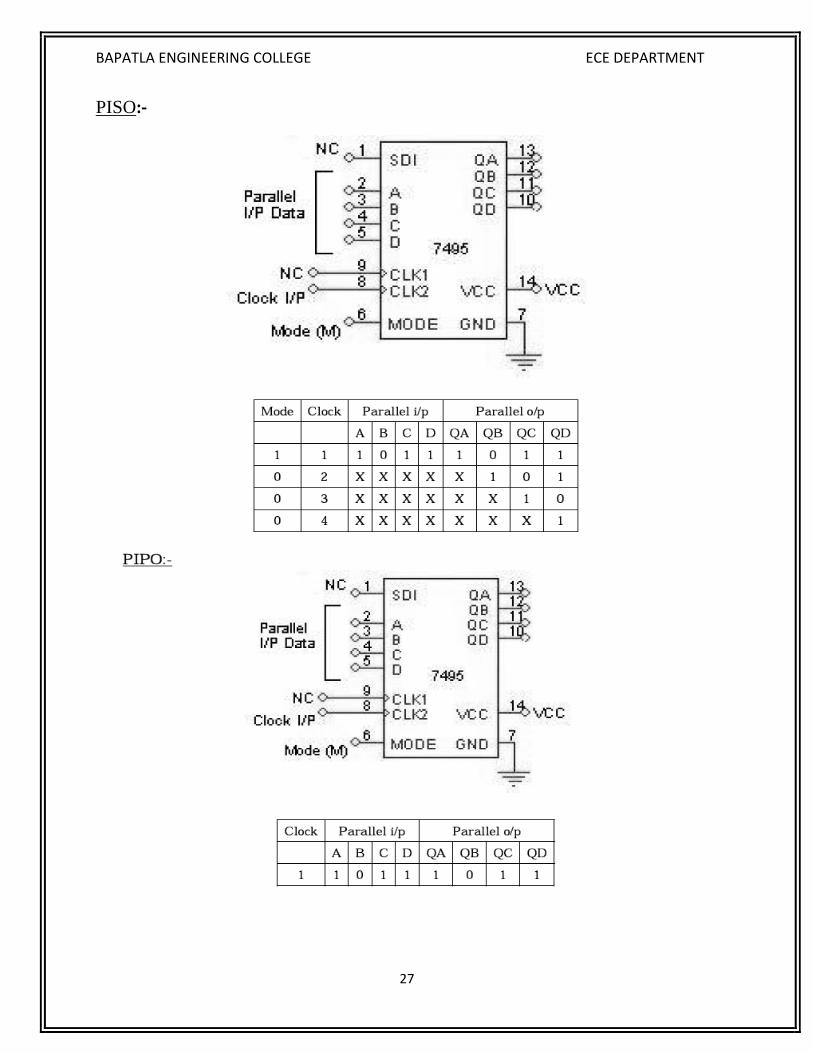
PISO:‐
BAPATLA ENGINEERING COLLEGE ECE DEPARTMENT
28
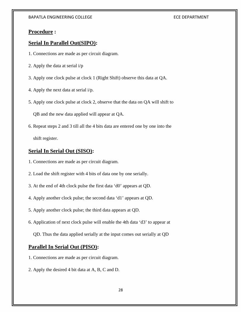
Procedure :
Serial In Parallel Out(SIPO):
1. Connections are made as per circuit diagram.
2. Apply the data at serial i/p
3. Apply one clock pulse at clock 1 (Right Shift) observe this data at QA.
4. Apply the next data at serial i/p.
5. Apply one clock pulse at clock 2, observe that the data on QA will shift to
QB and the new data applied will appear at QA.
6. Repeat steps 2 and 3 till all the 4 bits data are entered one by one into the
shift register.
Serial In Serial Out (SISO):
1. Connections are made as per circuit diagram.
2. Load the shift register with 4 bits of data one by one serially.
3. At the end of 4th clock pulse the first data ‘d0’ appears at QD.
4. Apply another clock pulse; the second data ‘d1’ appears at QD.
5. Apply another clock pulse; the third data appears at QD.
6. Application of next clock pulse will enable the 4th data ‘d3’ to appear at
QD. Thus the data applied serially at the input comes out serially at QD
Parallel In Serial Out (PISO):
1. Connections are made as per circuit diagram.
2. Apply the desired 4 bit data at A, B, C and D.

BAPATLA ENGINEERING COLLEGE ECE DEPARTMENT
29
3. Keeping the mode control M=1 apply one clock pulse. The data applied at
A, B, C and D will appear at QA, QB, QC and QD respectively.
4. Now mode control M=0. Apply clock pulses one by one and observe the
Data coming out serially at QD
Parallel In Parallel Out (PIPO):
1. Connections are made as per circuit diagram.
2. Apply the 4 bit data at A, B, C and D.
3. Apply one clock pulse at Clock 2 (Note: Mode control M=1).
4. The 4 bit data at A, B, C and D appears at QA, QB, QC and QD
respectively.
Precautions: All the connections should be made properly.
Result: shift registers using IC 7495 in all its modes i.e.SIPO/SISO, PISO/PIPO are verified.
BAPATLA ENGINEERING COLLEGE ECE DEPARTMENT
30
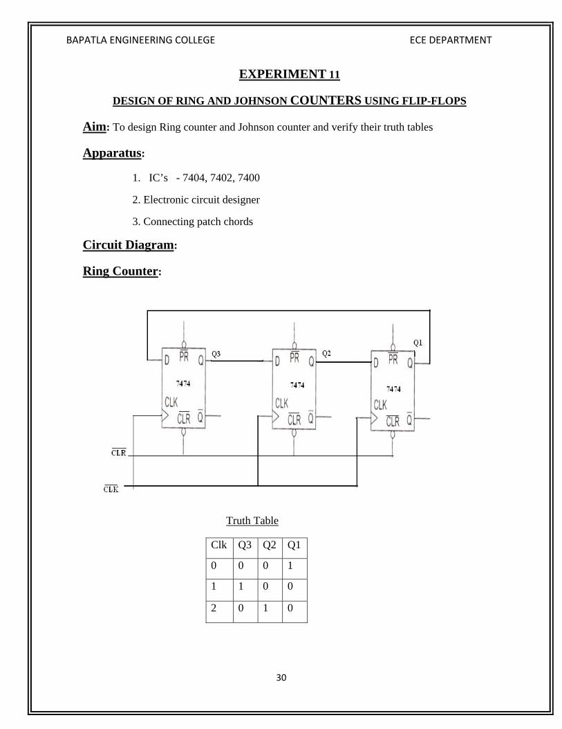
EXPERIMENT 11
DESIGN OF RING AND JOHNSON COUNTERS USING FLIP-FLOPS
Aim: To design Ring counter and Johnson counter and verify their truth tables
Apparatus:
1. IC’s - 7404, 7402, 7400
2. Electronic circuit designer
3. Connecting patch chords
Circuit Diagram:
Ring Counter:
Truth Table
Clk Q3 Q2 Q1
0 0 0 1
1 1 0 0
2 0 1 0
BAPATLA ENGINEERING COLLEGE ECE DEPARTMENT
31
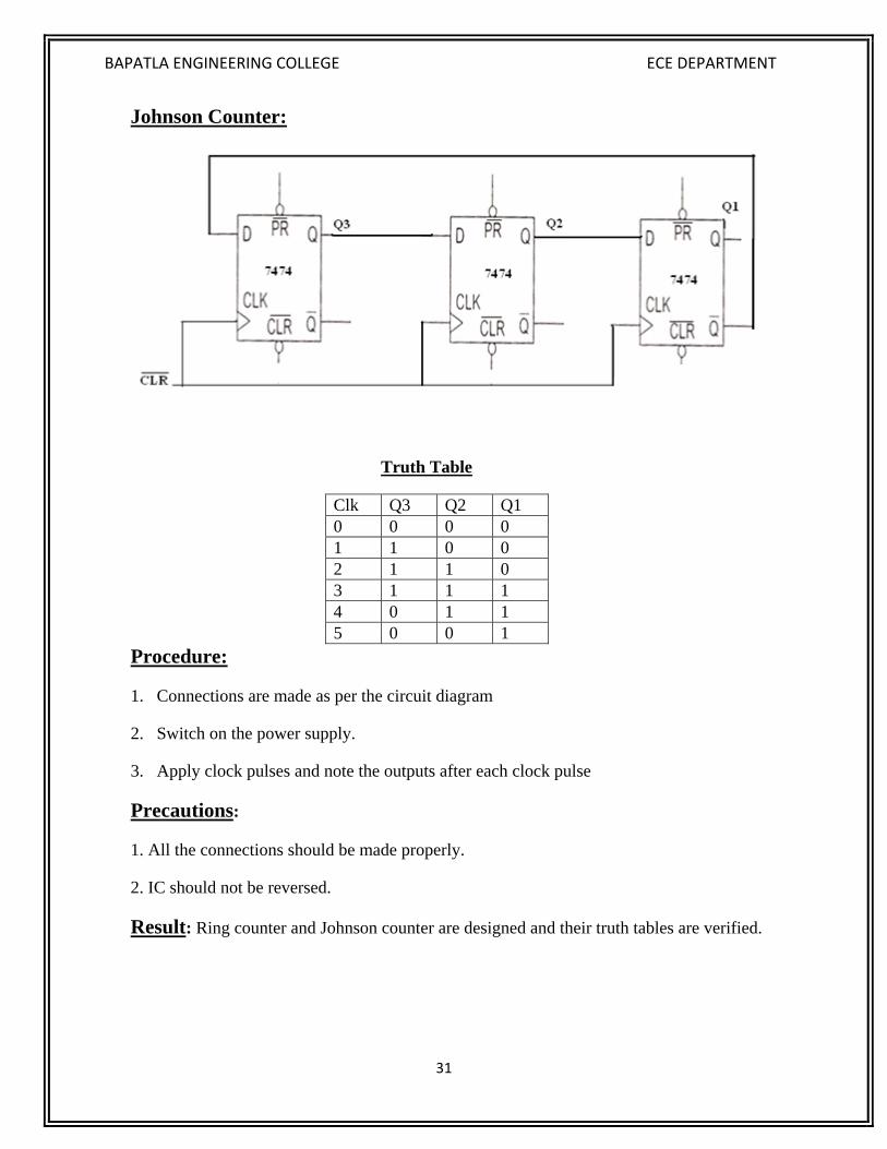
Johnson Counter:
Truth Table
Clk Q3 Q2 Q1 0 0 0 0 1 1 0 0 2 1 1 0 3 1 1 1 4 0 1 1 5 0 0 1
Procedure:
1. Connections are made as per the circuit diagram
2. Switch on the power supply.
3. Apply clock pulses and note the outputs after each clock pulse
Precautions:
1. All the connections should be made properly.
2. IC should not be reversed.
Result: Ring counter and Johnson counter are designed and their truth tables are verified.
BAPATLA ENGINEERING COLLEGE ECE DEPARTMENT
32
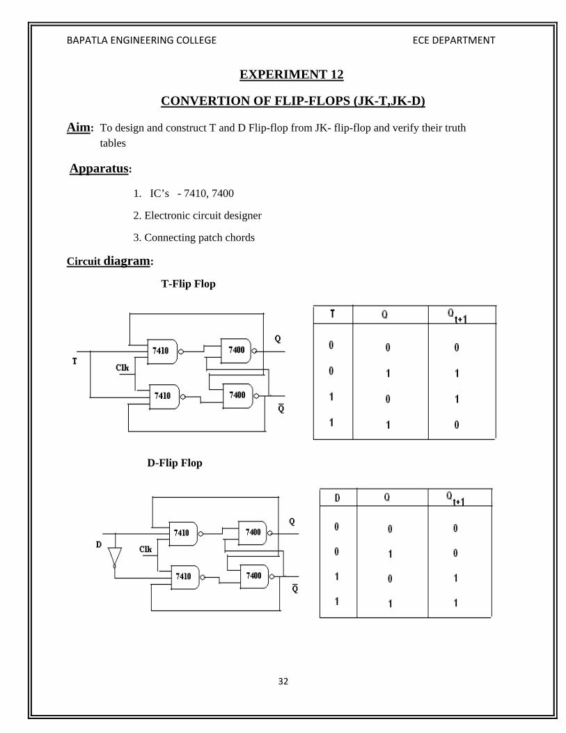
EXPERIMENT 12
CONVERTION OF FLIP-FLOPS (JK-T,JK-D)
Aim: To design and construct T and D Flip-flop from JK- flip-flop and verify their truth tables
Apparatus:
1. IC’s - 7410, 7400
2. Electronic circuit designer
3. Connecting patch chords
Circuit diagram:
T-Flip Flop
D-Flip Flop

BAPATLA ENGINEERING COLLEGE ECE DEPARTMENT
33
Procedure:
1. Connections are made as per the circuit diagram
2. Switch on the power supply
3. Apply different combinations of inputs and observe the out puts
Precautions:
1. All the connections should be made properly.
2. IC should not be reversed.
Result: T and D Flip-flop are designed and constructed from JK- flip-flop and their truth
tables are verified.
BAPATLA ENGINEERING COLLEGE ECE DEPARTMENT
34
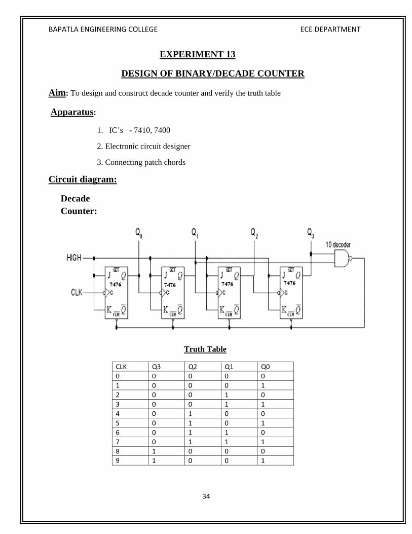
EXPERIMENT 13
DESIGN OF BINARY/DECADE COUNTER
Aim: To design and construct decade counter and verify the truth table
Apparatus:
1. IC’s - 7410, 7400
2. Electronic circuit designer
3. Connecting patch chords
Circuit diagram:
Decade Counter:
Truth Table
CLK Q3 Q2 Q1 Q0 0 0 0 0 0 1 0 0 0 1 2 0 0 1 0 3 0 0 1 1 4 0 1 0 0 5 0 1 0 1 6 0 1 1 0 7 0 1 1 1 8 1 0 0 0 9 1 0 0 1

BAPATLA ENGINEERING COLLEGE ECE DEPARTMENT
35
Procedure:
1. Connections are made as per the circuit diagram
2. Switch on the power supply.
3. Apply clock pulses and note the outputs after each clock pulse and note done the out puts Q3, Q2, Q1, Q0.
Precautions:
1. All the connections should be made properly.
2. IC should not be reversed.
Result: Decade counter is designed and truth tables are verified.
BAPATLA ENGINEERING COLLEGE ECE DEPARTMENT
36
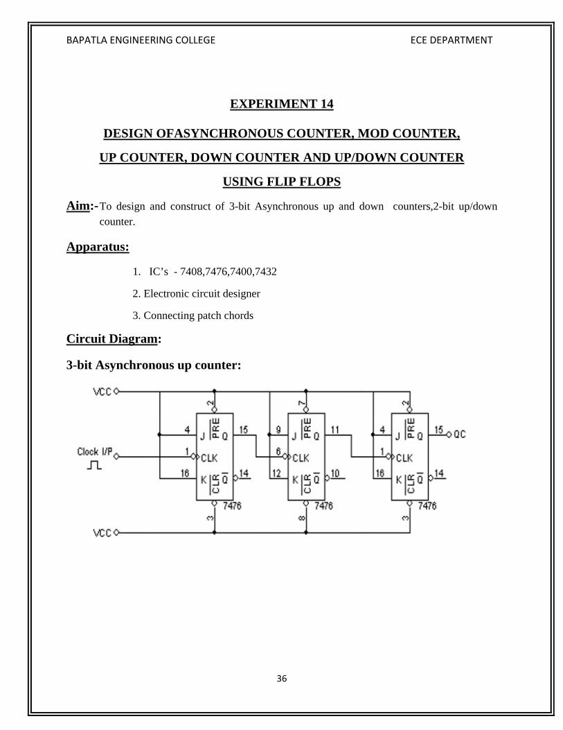
EXPERIMENT 14
DESIGN OFASYNCHRONOUS COUNTER, MOD COUNTER,
UP COUNTER, DOWN COUNTER AND UP/DOWN COUNTER
USING FLIP FLOPS
Aim:- To design and construct of 3-bit Asynchronous up and down counters,2-bit up/down counter.
Apparatus:
1. IC’s - 7408,7476,7400,7432
2. Electronic circuit designer
3. Connecting patch chords
Circuit Diagram:
3-bit Asynchronous up counter:
BAPATLA ENGINEERING COLLEGE ECE DEPARTMENT
37
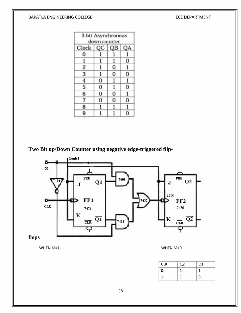
3-bit Asynchronous down counter:
TRUTH TABLE
BAPATLA ENGINEERING COLLEGE ECE DEPARTMENT
38
Two Bit up/Down Counter using negative edge-triggered flip-
flops
WHEN M=1 WHEN M=0
CLK Q2 Q1
0 1 1
1 1 0

BAPATLA ENGINEERING COLLEGE ECE DEPARTMENT
39
Procedure:
1. Connections are made as per the circuit diagram
2. Switch on the power supply.
3. Apply clock pulses and note the outputs after each clock pulse and note done the out puts.
Precautions:
1. All the connections should be made properly.
2. IC should not be reversed.
Result: 3-bit Asynchronous up and down counters,2-bit up/down counter are designed and
truth tables are verified.
2 0 1
3 0 0 CLK Q2 Q1
0 0 0
1 0 1
2 1 0
3 1 1
BAPATLA ENGINEERING COLLEGE ECE DEPARTMENT
40
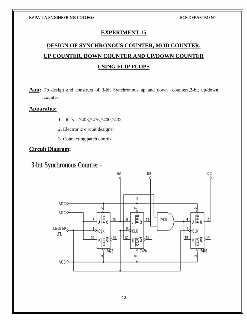
EXPERIMENT 15
DESIGN OF SYNCHRONOUS COUNTER, MOD COUNTER,
UP COUNTER, DOWN COUNTER AND UP/DOWN COUNTER
USING FLIP FLOPS
Aim:- To design and construct of 3-bit Synchronous up and down counters,2-bit up/down counter.
Apparatus:
1. IC’s - 7408,7476,7400,7432
2. Electronic circuit designer
3. Connecting patch chords
Circuit Diagram:
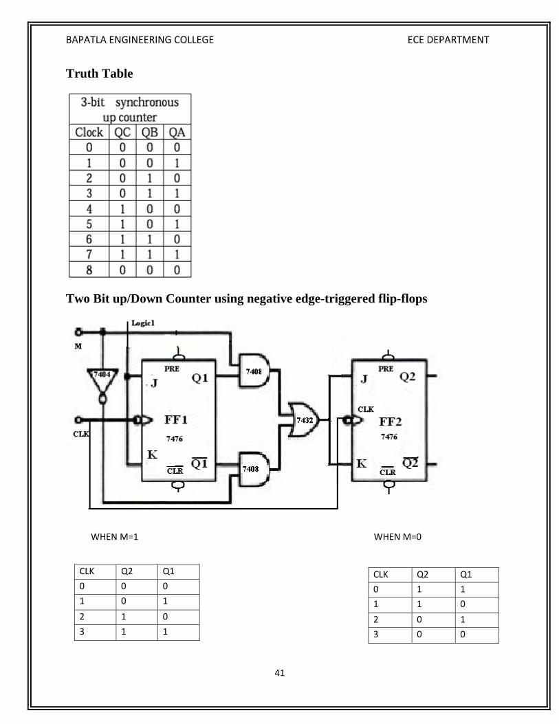
BAPATLA ENGINEERING COLLEGE ECE DEPARTMENT
41
Truth Table
Two Bit up/Down Counter using negative edge-triggered flip-flops
WHEN M=1 WHEN M=0
CLK Q2 Q1
0 1 1
1 1 0
2 0 1
3 0 0
CLK Q2 Q1
0 0 0
1 0 1
2 1 0
3 1 1

BAPATLA ENGINEERING COLLEGE ECE DEPARTMENT
42
Procedure:
1. Connections are made as per the circuit diagram
2. Switch on the power supply.
3. Apply clock pulses and note the outputs after each clock pulse and note done the out puts.
Precautions:
1. All the connections should be made properly.
2. IC should not be reversed.
Result: 3-bit Synchronous up and down counters,2-bit up/down counter are designed and
truth tables are verified.