bluetooth module hardware datasheet btm0608c2x...- 5 - chongqing jinou science and technology...
TRANSCRIPT

Chongqing JINOU Science and Technology Development Co.,
Ltd.
JO-0456
- i -
Chongqing JINOU Science and Technology Development Co., Ltd.
2016-6-30
Customize service and solution for wireless transportation products
Bluetooth Module Hardware Datasheet BTM0608C2X

Chongqing JINOU Science and Technology Development Co.,
Ltd.
JO-0456
- i -
Contents 1. Features ..................................................................................................................................... 1
2. Product Description ................................................................................................................... 1
3. Applications .............................................................................................................................. 2
4. Block Diagram .......................................................................................................................... 2
5. Device Details ........................................................................................................................... 3
6. Pin Descriptions ........................................................................................................................ 5
7. Electrical Specifications ............................................................................................................ 7
7.1 Absolute Maximum Ratings .......................................................................................... 7
7.2 Recommended Operating Conditions ........................................................................... 7
7.3 Regulator Enable ........................................................................................................... 8
7.4 Battery Charger ............................................................................................................. 8
7.5 USB ............................................................................................................................... 9
7.6 Stereo Codec: Analogue to Digital Converter ............................................................... 9
7.7 Stereo Codec: Digital to Analogue Converter ............................................................. 10
7.8 Digital.......................................................................................................................... 10
7.9 LED Driver Pads ......................................................................................................... 11
7.10 Auxiliary ADC ............................................................................................................ 11
7.11 Auxiliary DAC ............................................................................................................ 11
8. Power Consumption ................................................................................................................ 11
9. Programmable I/O Ports, PIO ................................................................................................. 12
9.1 Analogue I/O Ports, AIO ............................................................................................. 13
9.2 LED Drivers ................................................................................................................ 13
10. USB Interface ...................................................................................................................... 14
11. UART Interface ................................................................................................................... 14
12. Audio Interface ................................................................................................................... 16
12.1 Audio Input and Output............................................................................................... 17
12.2 Audio Codec Interface ................................................................................................ 17
12.3 Audio Codec Block Diagram ...................................................................................... 17
12.4 Codec Set-up ............................................................................................................... 18
12.5 ADC ............................................................................................................................ 18
12.6 ADC Sample Rate Selection ....................................................................................... 19
12.7 ADC Audio Input Gain ............................................................................................... 19
12.8 ADC Pre-amplifier and ADC Analogue Gain ............................................................. 19
12.9 ADC Digital Gain ....................................................................................................... 19
12.10 ADC Digital IIR Filter ............................................................................................ 20
12.11 DAC ........................................................................................................................ 20
12.12 DAC Sample Rate Selection ................................................................................... 20
12.13 DAC Digital Gain .................................................................................................... 20
12.14 DAC Analogue Gain ............................................................................................... 21
12.15 DAC Digital FIR Filter ............................................................................................ 21
12.16 IEC 60958 Interface ................................................................................................ 21

Chongqing JINOU Science and Technology Development Co.,
Ltd.
JO-0456
- i -
13. Physical Dimensions ........................................................................................................... 23

Chongqing JINOU Science and Technology Development Co.,
Ltd.
JO-0456
- 1 -
JO-0456
1. Features
Bluetooth Module Class 2
■ Bluetooth® v4.0 specification fully qualified software
■ Radio includes integrated balun
■ 80MHz RISC MCU and 80MIPS Kalimba DSP
■ 16Mb internal flash memory (64-bit wide, 45ns); optional support for 64Mb of external SPI
flash
■ Stereo codec with 2 channels of ADC and up to 6 microphone inputs (includes bias generators
and digital microphone support)
■ Support for CSR's latest CVC technology for narrow-band and wideband voice connections
including wind noise reduction
■ Audio interfaces: I²S, PCM and SPDIF
■ Serial interfaces: UART, USB 2.0 full-speed, I²C
■ Green (RoSH compliant and no antimony or halogenated flame retardants)
2. Product Description
JO-0456 consumer audio platform for wired and wireless applications integrates an
ultralow-power DSP and application processor with embedded flash memory, a high-performance
stereo codec, a power management subsystem,. The dual-core architecture with flash memory
enables manufacturers to easily differentiate their products with new features without extending
development cycles.
CSR's popular BlueCore5-Multimedia® platform is software-portable to the JO-0456, with

- 2 -
Chongqing JINOU Science and Technology Development Co.,
Ltd.
JO-0456
easy migration of a broad range of solutions from CSR's eXtension partners. This migration
enables rapid timeto-market deployment of a broad range of consumer electronics products.
The enhanced Kalimba DSP coprocessor with 80MIPS supports enhanced audio and DSP
applications.
3. Applications
Home Entertainment Ecosystem
■ TVs
■ Smart remote controllers
■ Wired or wireless soundbars
■ Wired or wireless speakers and headphones
Tablets / PCs / Mobile Connectivity
■ Wearable audio (on-the-go)
■ Wearable audio with sensors (health and wellbeing applications)
■ Wired or wireless stereo headphones for music/ gaming/multimedia content
■ Wired or wireless speakers
■ Wired or wireless speakerphones
■ Mono headsets for voice
The audio codec supports 2 ADC channels, up to 6 microphone inputs, stereo output and a
variety of audio standards.
4. Block Diagram

- 3 -
Chongqing JINOU Science and Technology Development Co.,
Ltd.
JO-0456
5. Device Details
Bluetooth low energy
■ Dual‑mode Bluetooth low energy radio
■ Support for Bluetooth basic rate / EDR and low energy connections
■ 3 Bluetooth low energy connections at the same time as basic rate A2DP
Bluetooth Radio
■ On‑chip balun (50Ω impedance in TX and RX modes)
■ No external trimming is required in production
■ Bluetooth v4.0 specification compliant hardware
■ Bluetooth v4.0 specification fully qualified software
Bluetooth Transmitter
■ 10dBm RF transmit power with level control from on‑chip 6‑bit DAC
■ Class 1, Class 2 and Class 3 support without the need for an external power amplifier or
TX/RX switch
Bluetooth Receiver
■ Receiver sensitivity: -90dBm (basic rate) and -92dBm (EDR)
■ Integrated channel filters
■ Digital demodulator for improved sensitivity and co‑channel rejection
■ Real‑time digitised RSSI available to application
■ Fast AGC for enhanced dynamic range
■ Channel classification for AFH
Kalimba DSP
■ Enhanced Kalimba DSP coprocessor, 80MIPS, 24‑bit fixed point core
■ Single‑cycle MAC; 24 x 24‑bit multiply and 56‑bit accumulate with improved architecture
and instructions for better performance
■ 32‑bit instruction word, dual 24‑bit data memory
■ 12K x 32‑bit program RAM including 1K instruction cache for executing out of internal
flash
■ 32K x 24‑bit + 32K x 24‑bit 2‑ bank data RAM
Audio Interfaces
■ Audio codec with 2 high‑ quality dedicated ADCs
■ 2 microphone bias generators and up to 2 analogue microphone inputs
■ Up to 6 digital microphone inputs (MEMS)
■ G.722 compatible, includes improved digital FIR filter path for stop‑ band attenuation
required for G.722 compliance
■ Enhanced side‑ tone gain control
■ Supported sample rates of 8, 11.025, 16, 22.05, 32, 44.1, 48 and 96kHz (DAC only)
Package Option
■ 19.812mm x 15.24mm x 1.93mm
Physical Interfaces
■ UART interface
■ USB 2.0 interface (full‑ speed)
■ Master and slave I²C interface

- 4 -
Chongqing JINOU Science and Technology Development Co.,
Ltd.
JO-0456
■ Up to 26 PIOs, i.e. 10 general purpose PIOs and unused digital interfaces are available as
PIOs
■ SPI debug and programming interface with read access disable locking
■ PCM, I²S and SPDIF interfaces
■ Dual/quad external serial flash memory interface
■ 1 LED drivers with PWM flasher on sleep clock
Battery Charger
■ Lithium ion / Lithium polymer battery charger with instant‑ on
■ Fast charging support up to 200mA with no external components
■ Higher charge currents using external pass device
■ Supports USB charge enumeration
■ Charger pre‑ calibrated by CSR
■ PSE compliance:
■ Design to JIS‑ C 8712/8714 (batteries)
■ Testing based on IEEE 1725
Auxiliary Features
■ Customer application space available
■ Crystal oscillator with built‑ in digital trimming
■ Clock request output to control external clock
■ Auxiliary ADC and DAC available to applications
Baseband and Software
■ 16Mb internal flash
■ Memory protection unit supporting accelerated VM
■ 56KB internal RAM, enables full‑ speed data transfer, mixed voice/data and full piconet
support
■ Logic for forward error correction, header error control, access code correlation, CRC,
demodulation, encryption bit stream generation, whitening and transmit pulse shaping
■ Transcoders for A‑ law, μ‑ law and linear voice via PCM and A‑ law, μ‑ law and CVSD
voice over air

- 5 -
Chongqing JINOU Science and Technology Development Co.,
Ltd.
JO-0456
6. Pin Descriptions
PIN Name Type Description
40 BT_RF2 RF Bluetooth 50Ω transmitter output / receiver input
54 UART_RX BU UART data input.
55 UART_RTS BU UART request to send, active low. Alternative function
PIO[16].
56 UART_TX BU UART data output.
57 UART_CTS BD UART clear to send, active low.
10 USB_P BB USB data plus with selectable internal 1.5kΩ pull-up
resistor
11 USB_N BB USB data minus
49 PCM_IN BD Synchronous data input. Alternative function PIO[17].
50 PCM_ CLK BD Synchronous data clock. Alternative function PIO[20].
51 PCM_ SYNC BD Synchronous data sync. Alternative function PIO[19].
52 PCM_OUT BD Synchronous data output. Alternative function PIO[18].
44 SPI_CLK ID SPI clock
45 SPI_MOSI ID SPI data input
46 SPI_MISO OD SPI data output
47 SPI_CS IU Chip select for SPI, active low
58 PIO[0] BI Programmable input / output line

- 6 -
Chongqing JINOU Science and Technology Development Co.,
Ltd.
JO-0456
1 PIO[1] BI
2 PIO[2] BI
3 PIO[3] BI
4 PIO[4] BI
5 PIO[5] BI
6 PIO[6] BI
7 PIO[7] BI
8 PIO[8] BI If interrupts are enabled on VREGENABLE the logic
signal is internally routed to PIO[8] to enable CSR8670
BGA to wake up from deep sleep when VREGENABLE
is pressed,
9 PIO[9] BI If interrupts are enabled on VCHG the logic signal is
internally routed to PIO[9] to enable CSR8670 BGA to
wake up from deep sleep when VCHG is pressed,
42 AIO[0] BB Analogue programmable input / output line
43 AIO[1] BB Analogue programmable input / output line
19 QSPI_FLASH_CLK BSD SPI flash clock. Alternative function PIO[21].
20 QSPI_FLASH_CS BSU SPI flash chip select. Alternative function PIO[23]
21 QSPI_FLASH_IO[0] BSD Serial quad I/O flash data bit 0.Alternative function
PIO[25].
22 QSPI_FLASH_IO[1] BSD Serial quad I/O flash data bit 1.Alternative function
PIO[26].
23 QSPI_FLASH_IO[2] BSD Serial quad I/O flash data bit 2.Alternative function
PIO[27].
24 QSPI_FLASH_IO[3] BSD Serial quad I/O flash data bit 3.Alternative function
PIO[28].
25 QSPI_SRAM_CLK BSD SPI RAM clock. Alternative function PIO[22].
26 QSPI_SRAM_CS# BSU SPI RAM chip select. Alternative function PIO[24].
27 MIC_LN AI Microphone input positive, left
28 MIC_LP AI Microphone input negative, left
31 M_RN AI Microphone input positive, right
32 M_RP AI Microphone input negative, right
30 MIC_BIAS_A AO Microphone bias A
33 MIC_BIAS_B AO Microphone bias B
34 SPKR_LN AO Speaker output negative, left
35 SPKR_LP AO Speaker output positive, left
36 SPKR_RN AO Speaker output negative, right
37 SPKR_RP AO Speaker output positive, right
48 LED[0] OC LED driver. Alternative function PO[29].

- 7 -
Chongqing JINOU Science and Technology Development Co.,
Ltd.
JO-0456
53 RST# IU Reset if low. Input debounced so must be low for >5ms to
cause a reset.
12 VBAT_SENSE Battery charger sense input
13 VBAT Battery positive terminal
14 VCHG Battery charger input
15 VOUT_3V3 Power Supply Input
17 CHG_EXT External battery charger control
18 VREGENABLE Regulator enable input
GND 16、29、38、39、41
BD = Bidirectional with weak pull-down
BU = Bidirectional with weak pull-up
BB = Bidirectional
BSD = Bidirectional with strong pull-down
BSU = Bidirectional with strong pull-up
OD = Output with weak pulldown
ID = Input with weak pulldown
IU = Input with strong pull-up
AI = Analogue in
AO = Analogue out
OC = Open drain
7. Electrical Specifications
7.1 Absolute Maximum Ratings
Rating Min Max Unit
Storage temperature -40 105 ℃
5V VCHG -0.4 5.75 / 6.50(a) V
3.3V VOUT_3V3 -0.4 3.60 V
Battery
VBAT_SENSE -0.4 5.75 V
VBAT -0.4 4.40 V
VREGENABLE -0.4 4.40 V
7.2 Recommended Operating Conditions
Rating Min Typ Max Unit
Operating temperature range -40 20 85 ℃
5V VCHG 4.75 5.00 5.75 V
3.3V VOUT_3V3 3.10 3.30 3.60 V
Battery
VBAT_SENSE 0 3.70 4.30 V
VBAT 2.80 3.70 4.30 V
VREGENABLE 0 3.70 4.25 V

- 8 -
Chongqing JINOU Science and Technology Development Co.,
Ltd.
JO-0456
7.3 Regulator Enable
VREGENABLE, Switching Threshold Min Typ Max Unit
Rising threshold - - 1.0 V
7.4 Battery Charger
Battery Charger Min Typ Max Unit
Input voltage, VCHG 4.75 5.00 5.75 V
Trickle Charge Mode Min Typ Max Unit
Charge current Itrickle, as percentage of fast charge
current
8 10 12 %
Vfast rising threshold - 2.9 - V
Vfast rising threshold trim step size - 0.1 - V
Vfast falling threshold - 2.8 - V
Fast Charge Mode Min Typ Max Unit
Charge current during
constant current mode, Ifast
Max, headroom > 0.55V 194 200 206 mA
Min, headroom > 0.55V - 10 - mA
Reduced headroom charge
current, as a percentage of
Ifast
Mid, headroom = 0.15V
50
-
100
%
Charge current step size - 10 - mA
Vfloat threshold, calibrated 4.16 4.20 4.24 V
Charge termination current Iterm, as percentage of Ifast 7 10 20 mA
Standby Mode Min Typ Max Unit
Voltage hysteresis on VBAT, Vhyst 100 - 150 mV
Error Charge Mode Min Typ Max Unit
Headroom(a) error falling threshold - 50 - mV
External Charge Mode(a) Min Typ Max Unit
Fast charge current, Ifast 200 - 500 mA
Control current into CHG_EXT 0 - 20 mA
Voltage on CHG_EXT 0 - 5.75 V
External pass device hfe 25 50 250 -
Sense voltage, between VBAT_SENSE and VBAT at
maximum current
195 200 205 mV

- 9 -
Chongqing JINOU Science and Technology Development Co.,
Ltd.
JO-0456
7.5 USB
Min Typ Max Unit
VDD_USB for correct USB operation 3.10 3.30 3.60 V
Input Threshold
VIL input logic level low - - 0.30 x
VDD_USB V
VIH input logic level high 0.70 x
VDD_USB - - V
Output Voltage Levels to Correctly Terminated USB Cable
VOL output logic level low 0 - 0.2 V
VOH output logic level high 2.80 - VDD_USB V
VDD_USB = VOUT_3V3
7.6 Stereo Codec: Analogue to Digital Converter
Analogue to Digital Converter
Parameter Conditions Min Typ Max Unit
Resolution - - - 16 Bits
Input Sample
Rate, Fsample - 8 - 48 kHz
SNR
fin = 1kHz
B/W=20Hz → F/2
(20kHz max)
A-Weighted
THD+N < 0.1%
1.6Vpk-pk input
Fsample
8kHz - 93 - dB
16kHz - 92 - dB
32kHz - 92 - dB
44.1kHz - 92 - dB
48kHz - 92 - dB
THD+N
fin = 1kHz
B/W=20Hz → F/2
(20kHz max)
1.6Vpk-pk input
Fsample
8kHz - 0.004 - %
48kHz - 0.008 - %
Digital gain Digital gain resolution = 1/32 -24 - 21.5 dB
Analogue gain
Pre-amplifier setting = 0dB, 9dB,
21dB or 30dB
Analogue setting = -3dB to 12dB in
3dB steps
-3
-
42
dB
Stereo separation (crosstalk) - -89 - dB
F = Fsample
- 10 -
Chongqing JINOU Science and Technology Development Co.,
Ltd.
JO-0456
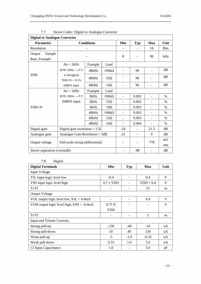
7.7 Stereo Codec: Digital to Analogue Converter
Digital to Analogue Converter
Parameter Conditions Min Typ Max Unit
Resolution - - - 16 Bits
Output Sample
Rate, Fsample - 8 - 96 kHz
SNR
fin = 1kHz
B/W=20Hz → F/2
A-Weighted
THD+N < 0.1%
0dBFS input
Fsample Load
48kHz 100kΩ - 96 - dB
48kHz 32Ω - 96 - dB
48kHz 16Ω - 96 - dB
THD+N
fin = 1kHz
B/W=20Hz → F/2
0dBFS input
Fsample Load
8kHz 100kΩ - 0.002 - %
8kHz 32Ω - 0.002 - %
8kHz 16Ω - 0.003 - %
48kHz 100kΩ - 0.003 - %
48kHz 32Ω - 0.003 - %
48kHz 16Ω - 0.004 - %
Digital gain Digital gain resolution = 1/32 -24 - 21.5 dB
Analogue gain Analogue Gain Resolution = 3dB -21 - 0 dB
Output voltage Full-scale swing (differential) - - 778 mV
rms
Stereo separation (crosstalk) - -88 - dB
7.8 Digital
Digital Terminals Min Typ Max Unit
Input Voltage
VIL input logic level low -0.4 - 0.4 V
VIH input logic level high 0.7 x VDD - VDD + 0.4 V
Tr/Tf - - 25 ns
Output Voltage
VOL output logic level low, lOL = 4.0mA - - 0.4 V
VOH output logic level high, lOH = -4.0mA 0.75 X
VDD
- - V
Tr/Tf - - 5 ns
Input and Tristate Currents
Strong pull-up -150 -40 -10 uA
Strong pull-down 10 40 150 uA
Weak pull-up -5 -1.0 -0.33 uA
Weak pull-down 0.33 1.0 5.0 uA
CI Input Capacitance 1.0 - 5.0 pF

- 11 -
Chongqing JINOU Science and Technology Development Co.,
Ltd.
JO-0456
7.9 LED Driver Pads
LED Driver Pads Min Typ Max Unit
Current, IPAD High impedance state - - 5 uA
Current sink state - - 10 mA
LED pad voltage, VPAD IPAD = 10mA - - 0.55 V
LED pad resistance VPAD < 0.5V - - 40 Ω
7.10 Auxiliary ADC
Auxiliary ADC Min Typ Max Unit
Resolution - - 10 Bits
Input voltage range(a) 0 - VDD V
Accuracy
(Guaranteed monotonic)
INL -1 - 1 LSB
DNL 0 - 1 LSB
Offset -1 - 1 LSB
Gain error -0.8 - 0.8 %
Input bandwidth - 100 - KHz
Conversion time 1.38 1.69 2.75 uS
Sample rate(b) - - 700 Samples/S
(a) LSB size = VDD /1023
(b) The auxiliary ADC is accessed through a VM function. The sample rate given is achieved as
part of this function.
VDD = 1.35V(Min=1.30V,Max=1.45V)
7.11 Auxiliary DAC
Auxiliary DAC Min Typ Max Unit
Resolution - - 10 Bits
Supply voltage, VDD_AUX 1.30 1.35 1.40 V
Output voltage range 0 - VDD_AUX V
Full-scale output voltage 1.30 1.35 1.40 V
LSB size 0 1.32 2.64 mV
Offset -1.32 0 1.32 mV
Integral non-linearity -1 0 1 LSB
Settling time(a) - - 250 ns
8. Power Consumption
DUT
Role Connection Type
Average
Current Unit
N/A Deep sleep With UART host connection - 60 uA
N/A Page scan Page = 1280ms interval
Window = 11.25ms - 242 uA
N/A Inquiry and
page scan
Inquiry = 1280ms interval
Page = 1280ms interval - 405 uA

- 12 -
Chongqing JINOU Science and Technology Development Co.,
Ltd.
JO-0456
Window = 11.25ms
Master ACL Sniff = 500ms, 1 attempt, 0 timeout DH1 139 uA
Master ACL Sniff = 1280ms, 8 attempts, 1 timeout DH1 127 uA
Master SCO Sniff = 100ms, 1 attempt, PCM HV3 8.7 mA
Master SCO Sniff = 100ms, 1 attempt, mono audio
codec HV3 10.5 mA
Master eSCO Setting S3, sniff = 100ms, PCM 2EV3 6.7 mA
Master eSCO Setting S3, sniff = 100ms, PCM 3EV3 6.4 mA
Master eSCO Setting S3, sniff = 100ms, mono audio
codec 2EV3 8.5 mA
Master eSCO Setting S3, sniff = 100ms, mono audio
codec 3EV3 8.2 mA
Slave ACL Sniff = 500ms, 1 attempt, 0 timeout DH1 150 uA
Slave ACL Sniff = 1280ms, 8 attempts, 1 timeout DH1 147 uA
Slave SCO Sniff = 100ms, 1 attempt, PCM HV3 9.1 mA
Slave SCO Sniff = 100ms, 1 attempt, mono audio
codec HV3 10.7 mA
Slave eSCO Setting S3, sniff = 100ms, PCM 2EV3 7.2 mA
Slave eSCO Setting S3, sniff = 100ms, PCM 3EV3 6.9 mA
Slave eSCO Setting S3, sniff = 100ms, mono audio
codec 2EV3 9.0 mA
Slave eSCO Setting S3, sniff = 100ms, mono audio
codec 3EV3 8.6 mA
9. Programmable I/O Ports, PIO
26 lines of programmable bidirectional I/O are available on the module. Some of the PIOs
on the module have alternative functions:
■ 3 digital microphone interfaces for control of up to 6 digital microphones:
Clock on any even PIOs as determined by the software
Data on any odd PIOs as determined by the software
■ I²C interface on any PIOs as determined by the software
Note:
If wake up of module is required via the VCHG pin, then the operation of PIO[9] is NC and
should be left unconnected. Otherwise, configuration of PIO[9] as a PIO is by setting
PSKEY_VCHG_REROUTE_INTERNALLY_VIA_PIO to 0xffff, for more information contact
CSR.
If wake up of module is required via the VREGENABLE pin, then the operation of PIO[8]
is NC and should be left unconnected. Otherwise, configuration of PIO[8] as a PIO is by setting
PSKEY_VREG_EN_REROUTE_INTERNALLY_VIA_PIO to 0xffff, for more information
contact CSR.
■ LED[0] directly map to PO[29]
■ PCM interface on PIO[20:17]
■ UART RTS on PIO[16]

- 13 -
Chongqing JINOU Science and Technology Development Co.,
Ltd.
JO-0456
■ Serial quad I/O flash interface on PIO[28:24]
Note:
See the relevant software release note for the implementation of these PIO lines, as they are
firmware buildspecific.
9.1 Analogue I/O Ports, AIO
Module has 2 general-purpose analogue interface pins, AIO[1:0], for accessing internal
circuitry and control signals. Auxiliary functions available on the analogue interface include a
10-bit ADC. Signals selectable on this interface include the band gap reference voltage. When
configured for analogue signals the voltage range is constrained by the analogue supply voltage.
9.2 LED Drivers
Module includes a 3-pad synchronised PWM LED driver for driving RGB LEDs for
producing a wide range of colours.
The terminals are open-drain outputs, so the LED must be connected from a positive supply
rail to the pad in series with a current-limiting resistor.
Figure 8.2: LED Equivalent Circuit
From Figure 8.2 it is possible to derive Equation 8.1 to calculate ILED. If a known value of
current is required through the LED to give a specific luminous intensity, then the value of
RLED is calculated.
Equation 8.1: LED Current
For the LED pads to act as resistance, the external series resistor, RLED, needs to be such
that the voltage drop across it, VR, keeps VPAD below 0.5V. Equation 8.2 also applies.

- 14 -
Chongqing JINOU Science and Technology Development Co.,
Ltd.
JO-0456
Equation 8.2: LED PAD Voltage
Note:
The LED current adds to the overall current. Conservative LED selection extends battery
life.
10. USB Interface
It has a full-speed (12Mbps) USB interface for communicating with other compatible digital
devices. The USB interface on this act as a USB peripheral, responding to requests from a master
host controller.
This supports the Universal Serial Bus Specification, Revision v2.0 (USB v2.0
Specification) and USB Battery Charging Specification, available from http://www.usb.org. For
more information on how to integrate the USB interface on it see the Bluetooth and USB Design
Considerations Application Note.
As well as describing USB basics and architecture, the application note describes:
■ Power distribution for high and low bus-powered configurations
■ Power distribution for self-powered configuration, which includes USB VBUS monitoring
(when VBUS is >3.1)
■ USB enumeration
■ Electrical design guidelines for the power supply and data lines, as well as PCB tracks and
the effects of ferrite beads
■ USB suspend modes and Bluetooth low-power modes:
Global suspend
Selective suspend, includes remote wake
Wake on Bluetooth, includes permitted devices and set-up prior to selective suspend
Suspend mode current draw
PIO status in suspend mode
Resume, detach and wake PIOs
■ Battery charging from USB, which describes dead battery provision, charge currents,
charging in suspend modes and USB VBUS voltage consideration
■ USB termination when interface is not in use
■ Internal modules, certification and non-specification compliant operation
11. UART Interface
This is a standard UART interface for communicating with other serial devices.
The UART interface provides a simple mechanism for communicating with other serial
devices using the RS-232 protocol.
- 15 -
Chongqing JINOU Science and Technology Development Co.,
Ltd.
JO-0456
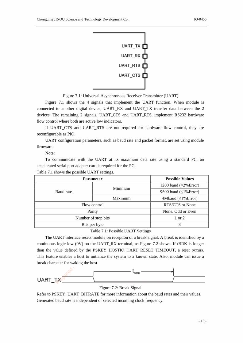
Figure 7.1: Universal Asynchronous Receiver Transmitter (UART)
Figure 7.1 shows the 4 signals that implement the UART function. When module is
connected to another digital device, UART_RX and UART_TX transfer data between the 2
devices. The remaining 2 signals, UART_CTS and UART_RTS, implement RS232 hardware
flow control where both are active low indicators.
If UART_CTS and UART_RTS are not required for hardware flow control, they are
reconfigurable as PIO.
UART configuration parameters, such as baud rate and packet format, are set using module
firmware.
Note:
To communicate with the UART at its maximum data rate using a standard PC, an
accelerated serial port adapter card is required for the PC.
Table 7.1 shows the possible UART settings.
Parameter Possible Values
Baud rate
Minimum 1200 baud (≤2%Error)
9600 baud (≤1%Error)
Maximum 4Mbaud (≤1%Error)
Flow control RTS/CTS or None
Parity None, Odd or Even
Number of stop bits 1 or 2
Bits per byte 8
Table 7.1: Possible UART Settings
The UART interface resets module on reception of a break signal. A break is identified by a
continuous logic low (0V) on the UART_RX terminal, as Figure 7.2 shows. If tBRK is longer
than the value defined by the PSKEY_HOSTIO_UART_RESET_TIMEOUT, a reset occurs.
This feature enables a host to initialize the system to a known state. Also, module can issue a
break character for waking the host.
Figure 7.2: Break Signal
Refer to PSKEY_UART_BITRATE for more information about the baud rates and their values.
Generated baud rate is independent of selected incoming clock frequency.

- 16 -
Chongqing JINOU Science and Technology Development Co.,
Ltd.
JO-0456
UART Configuration While Reset is Active
The UART interface is tristate while module is being held in reset. This enables the user to
connect other devices onto the physical UART bus. The restriction with this method is that any
devices connected to this bus must tristate when module reset is de-asserted and the firmware
begins to run.
12. Audio Interface
The audio interface circuit consists of:
■ Stereo/dual-mono audio codec
■ Dual analogue audio inputs
■ Dual analogue audio outputs
■ 6 digital MEMS microphone inputs
■ A configurable PCM, I²S or SPDIF interface
For more information on module audio path configuration see the CSR8670 Audio
Development Kit (DK‑ 8670‑ 10060‑ 1A).
Figure 9.1 shows the functional blocks of the interface. The codec supports stereo/dual-
mono playback and recording of audio signals at multiple sample rates with a 16-bit resolution.
The ADC and the DAC of the codec each contain 2 independent high-quality channels. Any
ADC or DAC channel runs at its own independent sample rate.
Figure 9.1: Audio Interface
The interface for the digital audio bus shares the same pins as the PCM codec interface
described in Section which means each of the audio buses are mutually exclusive in their usage.
Table 9.1 lists these alternative functions.
PCM Interface SPDIF Interface I²S Interface
PCM_OUT SPDIF_OUT SD_OUT
PCM_IN SPDIF_IN SD_IN
PCM_SYNC - WS
PCM_CLK - SCK
Table 9.1: Alternative Functions of the Digital Audio Bus Interface on the PCM Interface
- 17 -
Chongqing JINOU Science and Technology Development Co.,
Ltd.
JO-0456
12.1 Audio Input and Output
The audio input circuitry consists of:
■ 2 independent 16-bit high-quality ADC channels:
Programmable as either microphone or line input
Programmable as either stereo or dual-mono inputs
Multiplexed with 2 of the digital microphone inputs.
Each channel is independently configurable to be either single-ended or fully
differential
Each channel has an analogue and digital programmable gain stage for optimisation of
different microphones
■ 6 digital MEMS microphone channels, of which 4 have independent codec channels and 2
share their codecs with the 2 high-quality audio inputs
The audio output circuitry consists of a dual differential class A-B output stage.
Note:
Module is designed for a differential audio output. If a single-ended audio output is required,
use an external differential to single-ended converter.
12.2 Audio Codec Interface
The main features of the interface are:
■ Stereo and mono analogue input for voice band and audio band
■ Stereo and mono analogue output for voice band and audio band
■ Support for stereo digital audio bus standards such as I²S
■ Support for IEC-60958 standard stereo digital audio bus standards, e.g. SPDIF and AES3
(also known as AES/EBU)
■ Support for PCM interfaces including PCM master codecs that require an external system
clock Important Note:
To avoid any confusion regarding stereo operation this data sheet explicitly states which is
the left and right channel for audio output. With respect to audio input, software and any registers,
channel 0 or channel A represents the left channel and channel 1 or channel B represents the right
channel.
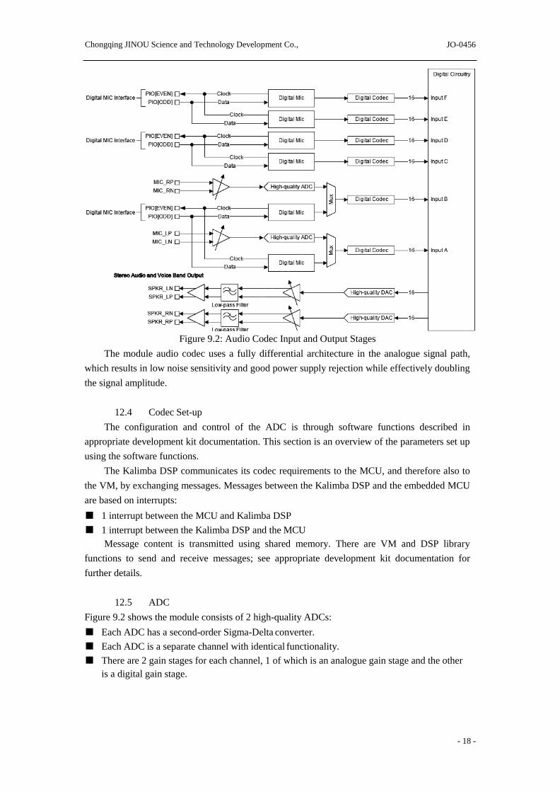
12.3 Audio Codec Block Diagram
Stereo Audio, Voice Band and Digital Microphone Input
Note:
L/R pins on digital microphones
pulled up or down on the PCB
- 18 -
Chongqing JINOU Science and Technology Development Co.,
Ltd.
JO-0456
Figure 9.2: Audio Codec Input and Output Stages
The module audio codec uses a fully differential architecture in the analogue signal path,
which results in low noise sensitivity and good power supply rejection while effectively doubling
the signal amplitude.
12.4 Codec Set-up
The configuration and control of the ADC is through software functions described in
appropriate development kit documentation. This section is an overview of the parameters set up
using the software functions.
The Kalimba DSP communicates its codec requirements to the MCU, and therefore also to
the VM, by exchanging messages. Messages between the Kalimba DSP and the embedded MCU
are based on interrupts:
■ 1 interrupt between the MCU and Kalimba DSP
■ 1 interrupt between the Kalimba DSP and the MCU
Message content is transmitted using shared memory. There are VM and DSP library
functions to send and receive messages; see appropriate development kit documentation for
further details.
12.5 ADC
Figure 9.2 shows the module consists of 2 high-quality ADCs:
■ Each ADC has a second-order Sigma-Delta converter.
■ Each ADC is a separate channel with identical functionality.
■ There are 2 gain stages for each channel, 1 of which is an analogue gain stage and the other
is a digital gain stage.

- 19 -
Chongqing JINOU Science and Technology Development Co.,
Ltd.
JO-0456
12.6 ADC Sample Rate Selection
Each ADC supports the following pre-defined sample rates, although other rates are
programmable, e.g. 40kHz:
■ 8kHz
■ 11.025kHz
■ 16kHz
■ 22.050kHz
■ 24kHz
■ 32kHz
■ 44.1kHz
■ 48kHz
12.7 ADC Audio Input Gain
Figure 9.3 shows that the CSR8670 BGA audio input gain consists of:
■ An analogue gain stage based on a pre-amplifier and an analogue gain amplifier
■ A digital gain stage
Figure 9.3: Audio Input Gain
12.8 ADC Pre-amplifier and ADC Analogue Gain
Module has an analogue gain stage based on an ADC pre-amplifier and ADC analogue amplifier:
■ The ADC pre-amplifier has 4 gain settings: 0dB, 9dB, 21dB and 30dB
■ The ADC analogue amplifier gain is -3dB to 12dB in 3dB steps
■ The overall analogue gain for the pre-amplifier and analogue amplifier is -3dB to 42dB in
3dB steps, see Figure 9.3
■ At mid to high gain levels it acts as a microphone pre-amplifier
■ At low gain levels it acts as an audio line level amplifier
12.9 ADC Digital Gain
A digital gain stage inside the ADC varies from -24dB to 21.5dB, see Table 9.2. There is
also a fine gain interface with a 9-bit gain setting allowing gain changes in 1/32 steps, for more
infomation contact CSR.
The firmware controls the audio input gain.

- 20 -
Chongqing JINOU Science and Technology Development Co.,
Ltd.
JO-0456
Table 9.2: ADC Audio Input Gain Rate
12.10 ADC Digital IIR Filter
The ADC contains 2 integrated anti-aliasing filters:
■ A long IIR filter suitable for music (>44.1kHz)
■ G.722 filter is a digital IIR filter that improves the stop-band attenuation required for G.722
compliance (which is the best selection for 8kHz / 16kHz / voice)
For more information contact www.jinoux.com.
12.11 DAC
The DAC consists of:
■ 2 fourth-order Sigma-Delta converters enabling 2 separate channels that are identical in
functionality, as Figure 9.2 shows.
■ 2 gain stages for each channel, 1 of which is an analogue gain stage and the other is a digital
gain stage.
12.12 DAC Sample Rate Selection
Each DAC supports the following sample rates:
■ 8kHz
■ 11.025kHz
■ 16kHz
■ 22.050kHz
■ 32kHz
■ 40kHz
■ 44.1kHz
■ 48kHz
■ 96kHz
12.13 DAC Digital Gain
A digital gain stage inside the DAC varies from -24dB to 21.5dB, see Table 9.3. There is also a
fine gain interface with a 9-bit gain setting enabling gain changes in 1/32 steps, for more

- 21 -
Chongqing JINOU Science and Technology Development Co.,
Ltd.
JO-0456
information contact CSR.
The overall gain control of the DAC is controlled by the firmware. Its setting is a combined
function of the digital and analogue amplifier settings.
Table 9.3: DAC Digital Gain Rate Selection
12.14 DAC Analogue Gain
Table 9.4 shows that the DAC analogue gain stage consists of 8 gain selection values that
represent seven 3dB steps.
The firmware controls the overall gain control of the DAC. Its setting is a combined
function of the digital and analogue amplifier settings.
Table 9.4: DAC Analogue Gain Rate Selection
12.15 DAC Digital FIR Filter
The DAC contains an integrated digital FIR filter with the following modes:
■ A default long FIR filter for best performance at ≥ 44.1kHz.
■ A short FIR to reduce latency.
■ A narrow FIR (a very sharp roll-off at Nyquist) for G.722 compliance. Best for 8kHz / 16kHz.
12.16 IEC 60958 Interface
The IEC 60958 interface is a digital audio interface that uses bi-phase coding to minimise
the DC content of the transmitted signal and enables the receiver to decode the clock information
from the transmitted signal. The IEC 60958 specification is based on the 2 industry standards:

- 22 -
Chongqing JINOU Science and Technology Development Co.,
Ltd.
JO-0456
■ AES3 (also known as AES/EBU)
■ Sony and Philips interface specification SPDIF
The interface is compatible with IEC 60958-1, IEC 60958-3 and IEC 60958-4.
The SPDIF interface signals are SPDIF_IN and SPDIF_OUT and are shared on the PCM
interface pins. The input and output stages of the SPDIF pins interface to:
■ A 75Ω coaxial cable with an RCA connector, see Figure 9.4
■ An optical link that uses Toslink optical components, see Figure 9.5.
Figure 9.4: Example Circuit for SPDIF Interface (Co-axial)
Figure 9.5: Example Circuit for SPDIF Interface (Optical)

- 23 -
Chongqing JINOU Science and Technology Development Co.,
Ltd.
JO-0456
13. Physical Dimensions
A B C D E F G H J K L Unit
750 600 50 40 60 90 110 25 30 74 107 mil
19.05 15.24 1.27 1.016 1.524 2.286 2.794 0.635 0.762 1.88 2.718 mm
Deviation:±0.1mm