ch 01 -os8e - santa monica...
TRANSCRIPT

Chapter 1Computer System
OverviewEighth Edition
By William Stallings
Operating Systems:Internals
and Design
Principles

Operating SystemOperating System
�Exploits the hardware resources of one or
more processors
�Provides a set of services to system users
�Manages secondary memory and I/O devices

Basic ElementsBasic Elements

ProcessorProcessor

Main MemoryMain Memory
�Volatile
�Contents of the memory is lost
when the computer is shut
down
�Referred to as real memory or
primary memory

I/O ModulesI/O Modules

System BusSystem Bus
�Provides for communication among
processors, main memory,
and I/O modules

PC MAR
IR MBR
I/O AR
I/O BR
CPU Main Memory
System
Bus
I/O Module
Buffers
Instruction
0
1
2
n - 2
n - 1
Data
Data
Data
Data
Instruction
Instruction
Figure 1.1 Computer Components: Top-Level View
PC = Program counter
IR = Instruction register
MAR = Memory address register
MBR = Memory buffer register
I/O AR = Input/output address register
I/O BR = Input/output buffer register
Execution
unit

MicroprocessorMicroprocessor
�Invention that brought about desktop and handheld computing
�Processor on a single chip
�Fastest general purpose processor
�Multiprocessors
�Each chip (socket) contains multiple processors (cores)

Graphical Processing Graphical Processing Units (GPUUnits (GPU’’s)s)
�Provide efficient computation on arrays of data using Single-Instruction Multiple Data (SIMD) techniques
�Used for general numerical processing
�Physics simulations for games
�Computations on large spreadsheets

Digital Signal ProcessorsDigital Signal Processors(DSPs)(DSPs)
�Deal with streaming signals such as audio or video
�Used to be embedded in devices like modems
�Encoding/decoding speech and video (codecs)
�Support for encryption and security

System on a ChipSystem on a Chip(SoC)(SoC)
�To satisfy the requirements of handheld
devices, the microprocessor is giving
way to the SoC
�Components such as DSPs, GPUs,
codecs and main memory, in
addition to the CPUs and
caches, are on the same chip
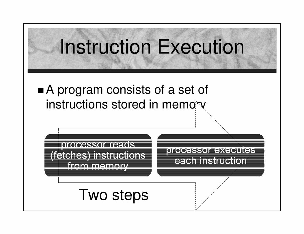
Instruction ExecutionInstruction Execution
�A program consists of a set of instructions stored in memory
Two steps
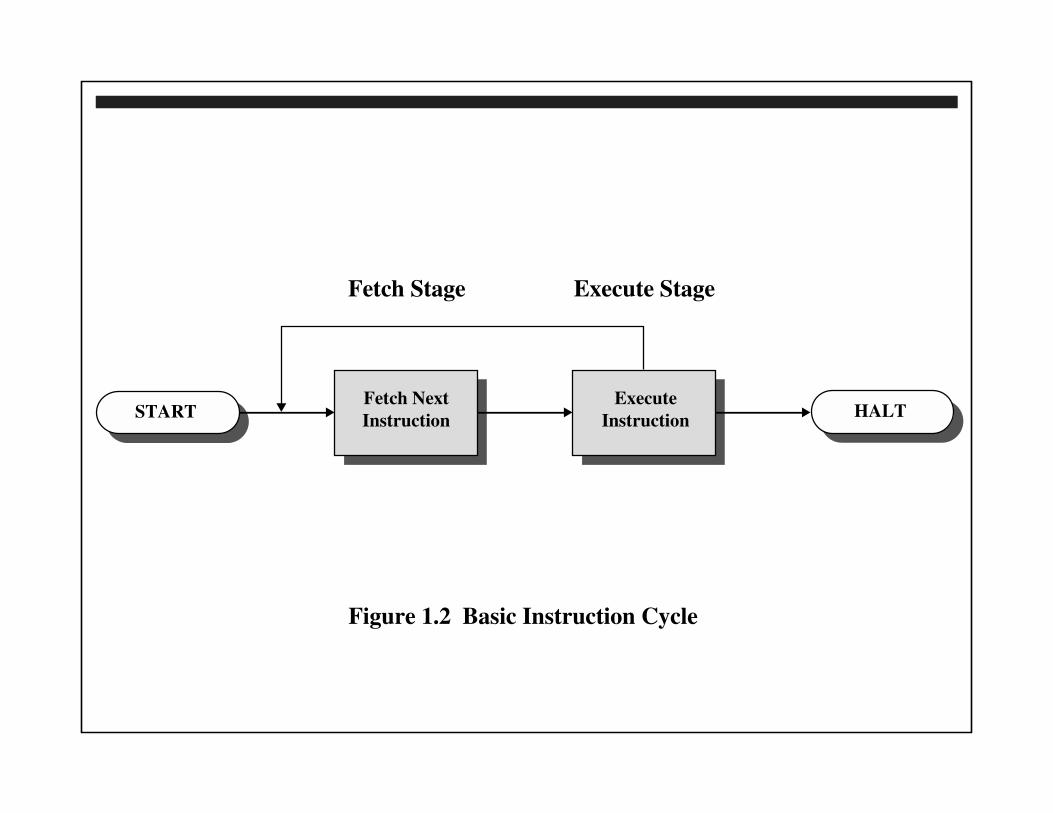
START HALTFetch Next
Instruction
Fetch Stage Execute Stage
Execute
Instruction
Figure 1.2 Basic Instruction Cycle
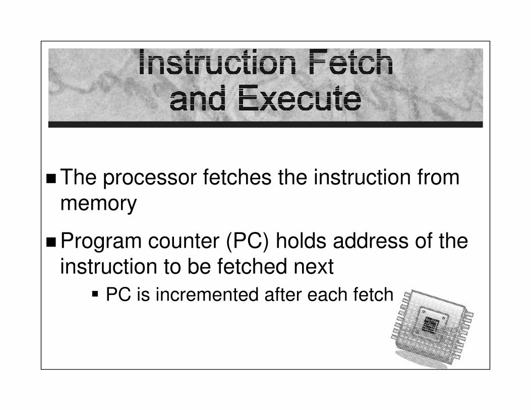
�The processor fetches the instruction from memory
�Program counter (PC) holds address of the instruction to be fetched next
� PC is incremented after each fetch

Instruction Register (IR)Instruction Register (IR)
Fetched instruction is
loaded into Instruction Register (IR)
� Processor interprets the
instruction and
performs required
action:
� Processor-memory
� Processor-I/O
� Data processing
� Control

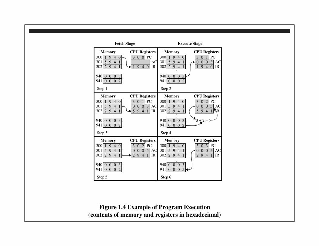
2
PC300
CPU RegistersMemory
Fetch Stage Execute Stage
3 0 01 9 4 0301 5 9 4 1302 2 9 4 1
940 0 0 0 3941 0 0 0 2
ACIR1 9 4 0
Step 1
•
•
PC300
CPU RegistersMemory
3 0 11 9 4 0301 5 9 4 1302 2 9 4 1
940 0 0 0 3941 0 0 0 2
ACIR1 9 4 0
0 0 0 3
Step 2
•
•
PC300
CPU RegistersMemory
3 0 10 0 0 5
0 0 0 5
0 0 0 3
0 0 0 5
1 9 4 0301 5 9 4 1302 2 9 4 1
940 0 0 0 3941 0 0 0 2
ACIR5 9 4 1
Step 3
•
•
PC300
CPU RegistersMemory
3 0 21 9 4 0301 5 9 4 1302 2 9 4 1
1
940 0 0 0 3941 0 0 0 2
ACIR5 9 4 1
Step 4
•
•
PC300
CPU RegistersMemory
3 01 9 4 0301 5 9 4 1302 2 9 4 1
940 0 0 0 3941 0 0 0 2
ACIR2 9 4 1
Step 5
•
•
PC300
CPU RegistersMemory
3 0 31 9 4 0301 5 9 4 1302 2 9 4 1
940 0 0 0 3941 0 0 0 5
ACIR2 9 4 1
Step 6
•
•
3 + 2 = 5
Figure 1.4 Example of Program Execution
(contents of memory and registers in hexadecimal)

InterruptsInterrupts
� Interrupt the normal sequencing of the processor
�Provided to improve processor utilization� most I/O devices are slower than the processor
� processor must pause to wait for device
� wasteful use of the processor

Table 1.1 Classes of Interrupts
Program Generated by some condition that occurs as a
result of an instruction execution, such as arithmetic
overflow, division by zero, attempt to execute an illegal machine
instruction, and reference outside a user's allowed memory
space.
Timer Generated by a timer within the processor. This allows the
operating system to perform certain functions on a regular
basis.
I/O Generated by an I/O controller, to signal normal
completion of an operation or to signal a variety of error
conditions.
Hardware Generated by a failure, such as power failure or memory
failure parity error.
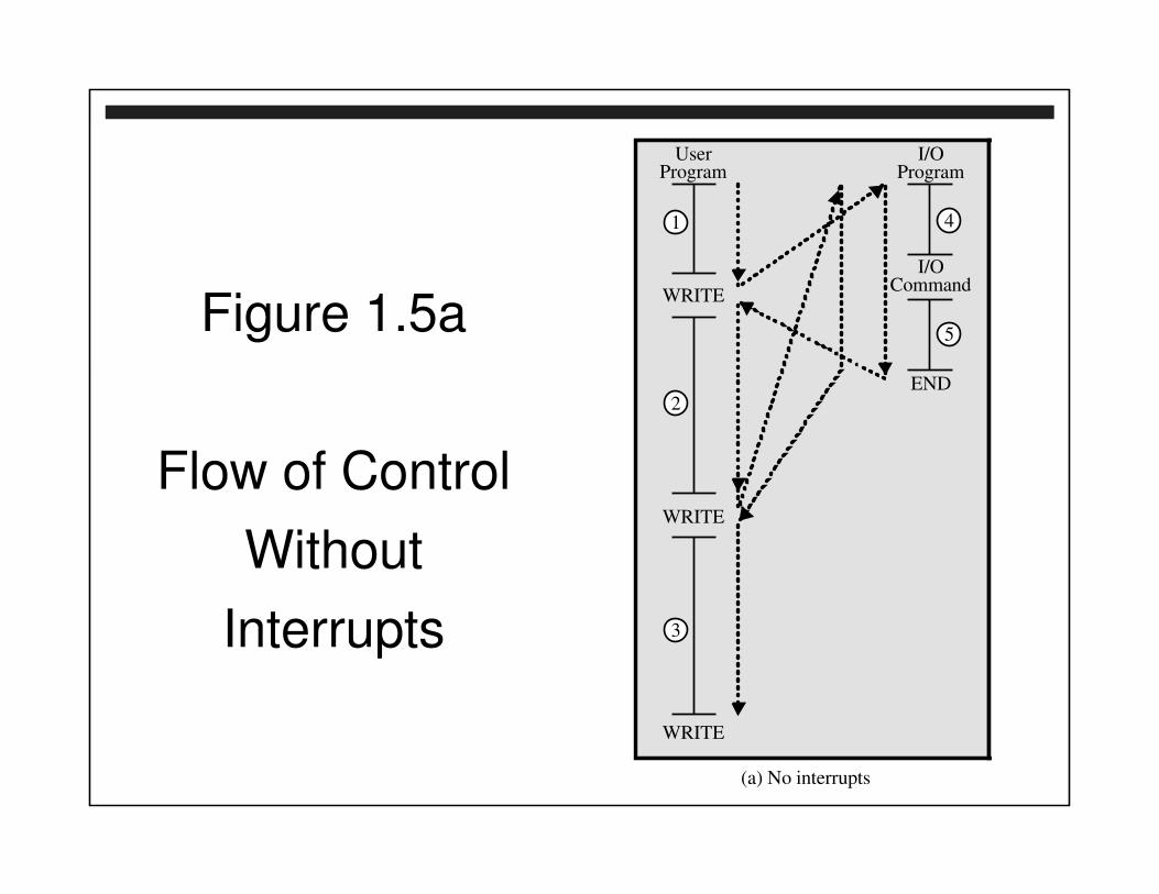
Figure 1.5a
Flow of Control
Without
Interrupts
UserProgram
WRITE
WRITE
WRITE
I/OProgram
I/OCommand
END
1
2
3
4
5
(a) No interrupts

Figure 1.5b
Short I/O Wait
UserProgram
WRITE
WRITE
WRITE
I/OProgram
I/OCommand
InterruptHandler
END
1
2a
2b
3a
3b
4
5
(b) Interrupts; short I/O wait
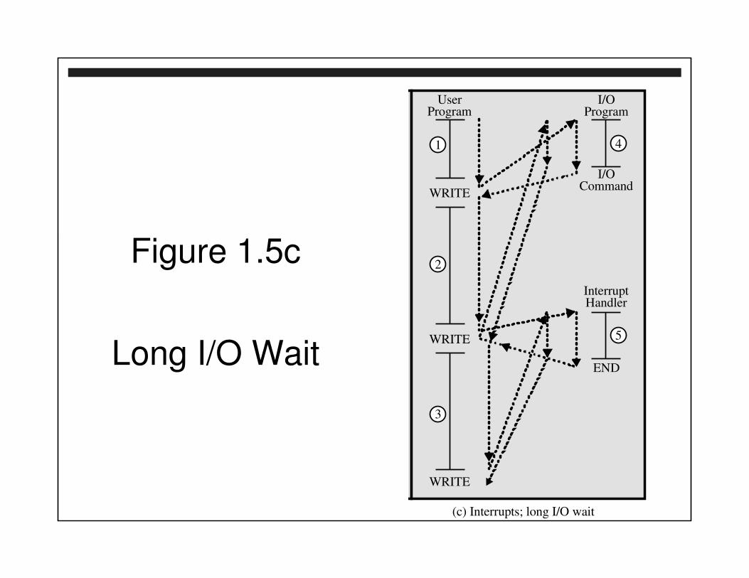
Figure 1.5c
Long I/O Wait
2
3
UserProgram
WRITE
WRITE
WRITE
I/OProgram
I/OCommand
InterruptHandler
END
1 4
5
(c) Interrupts; long I/O wait

1
2
i
i + 1
M
Interrupt
occurs here
User Program Interrupt Handler
Figure 1.6 Transfer of Control via Interrupts

START
HALT
Fetch next
instruction
Fetch Stage Execute Stage Interrupt Stage
Interrupts
Disabled
Interrupts
Enabled
Execute
instruction
Check for
interrupt;
initiate interrupt
handler
Figure 1.7 Instruction Cycle with Interrupts

4
1
5 5
2
5
3
4
Time
I/O operation;
processor waits
I/O operation
concurrent with
processor executing
I/O operation
concurrent with
processor executingI/O operation;
processor waits
4
2a
1
2b
4
3a
5
3b
(a) Without interrupts
(b) With interrupts
Figure 1.8 Program Timing: Short I/O Wait

4
1
5
2
5
3
4
Time
4
2
1
5
4
(a) Without interrupts
(b) With interrupts
Figure 1.9 Program Timing: Long I/O Wait
3
5
I/O operation;
processor waits
I/O operation;
processor waits
I/O operation
concurrent with
processor executing;
then processor
waits
I/O operation
concurrent with
processor executing;
then processor
waits

Device controller or
other system hardware
issues an interrupt
Processor finishes
execution of current
instruction
Processor signals
acknowledgment
of interrupt
Processor pushes PSW
and PC onto control
stack
Processor loads new
PC value based on
interrupt
Save remainder of
process state
information
Process interrupt
Restore process state
information
Restore old PSW
and PC
Hardware Software
Figure 1.10 Simple Interrupt Processing
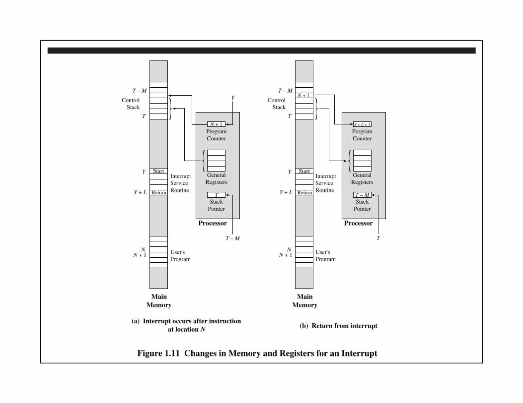
Start
N + 1
Y + L
N
Y
Y
T
Return
User's
Program
Main
Memory
Processor
General
Registers
Program
Counter
Stack
Pointer
N + 1
T – M
T – M
T
Control
Stack
Interrupt
Service
Routine
User's
Program
Interrupt
Service
Routine
(a) Interrupt occurs after instruction
at location N(b) Return from interrupt
Figure 1.11 Changes in Memory and Registers for an Interrupt
Start
N + 1
Y + L
N
Y
T
Return
Main
Memory
Processor
General
Registers
Program
Counter
Stack
Pointer
Y + L + 1
T – M
T – M
T
Control
Stack
N + 1

Multiple InterruptsMultiple Interrupts

User Program
Interrupt
Handler X
Interrupt
Handler Y
(a) Sequential interrupt processing
(b) Nested interrupt processing
Figure 1.12 Transfer of Control with Multiple Interrupts
User Program
Interrupt
Handler X
Interrupt
Handler Y

User ProgramPrinter
interrupt service routine
Communication
interrupt service routine
Disk
interrupt service routine
Figure 1.13 Example Time Sequence of Multiple Interrupts
t = 10
t = 40
t = 15
t = 25
t = 25
t = 35
t = 0

Memory HierarchyMemory Hierarchy
� Major constraints in memory
� amount
� speed
� expense
� Memory must be able to keep up with the
processor
� Cost of memory must be reasonable in relationship
to the other components

Memory RelationshipsMemory Relationships

The Memory HierarchyThe Memory Hierarchy
�Going down the hierarchy:
� decreasing cost per bit
� increasing capacity
� increasing access time
� decreasing frequency of
access to the memory by
the processor
Figure 1.14 The Memory Hierarchy
InboardM
emory
OutboardStorage
Off-lineStorage
Main
Memory
Magnetic
Disk
CD-ROM
CD-RW
DVD-RW
DVD-RAM
Blu-Ray
Magnetic
Tape
Cache
Reg-
isters

0
T1
T1 + T2
T2
1Fraction of accesses involving only Level 1 (Hit ratio)
Aver
age
acce
ss t
ime
Figure 1.15 Performance of a Simple Two-Level Memory

�Memory references by the processor tend to cluster
�Data is organized so that the percentage of accesses to each successively lower level is substantially less than that of the level above
�Can be applied across more than two levels of memory


� Invisible to the OS
� Interacts with other memory management hardware
� Processor must access memory at least once per
instruction cycle
� Processor execution is limited by memory cycle time
� Exploit the principle of locality with a small, fast memory

CPU
Word Transfer
Fast
Fastest FastLessfast
Slow
Slow
Block Transfer
Cache Main Memory
Figure 1.16 Cache and Main Memory
(a) Single cache
(b) Three-level cache organization
CPULevel 1
(L1) cache
Level 2
(L2) cache
Level 3
(L3) cache
Main
Memory

Memory
address
0
1
2
0
1
2
C - 1
3
2n - 1
Word
Length
Block Length
(K Words)
Block 0
(K words)
Block M – 1
Line
Number Tag Block
(b) Main memory
(a) Cache
Figure 1.17 Cache/Main-Memory Structure

Receive address
RA from CPU
Is block
containing RA
in cache?
Fetch RA word
and deliver
to CPU
DONE
Access main
memory for block
containing RA
Allocate cache
slot for main
memory block
Deliver RA word
to CPU
Load main
memory block
into cache slot
Figure 1.18 Cache Read Operation
START
No
RA - read address
Yes


Cache and Block SizeCache and Block Size

Mapping FunctionMapping Function
∗ Determines which cache location the block will occupy

Replacement AlgorithmReplacement Algorithm
� chooses which block to replace when a new block is to be loaded into the cache
�Least Recently Used (LRU) Algorithm� effective strategy is to replace a block that has been
in the cache the longest with no references to it
� hardware mechanisms are needed to identify the least recently used block

Write PolicyWrite Policy

I/O TechniquesI/O Techniques
∗ When the processor encounters an instruction relating to I/O, it executes that instruction by issuing a command to the appropriate I/O module

Programmed I/OProgrammed I/O
� The I/O module performs the requested action then sets the appropriate bits in the I/O status register
� The processor periodically checks the status of the I/O module until it determines the instruction is complete
� With programmed I/O the performance level of the entire system is severely degraded

InterruptInterrupt--Driven I/ODriven I/O

InterruptInterrupt--Driven I/ODriven I/ODrawbacksDrawbacks
�Transfer rate is limited by the speed with which the processor can test and service a device
�The processor is tied up in managing an I/O transfer
� a number of instructions must be executed for each I/O transfer

Direct Memory AccessDirect Memory Access(DMA)(DMA)
∗ Performed by a separate module on the system bus or incorporated into an I/O module

�Transfers the entire block of data directly to and from memory without going through the processor
� processor is involved only at the beginning and end of the transfer
� processor executes more slowly during a transfer when processor access to the bus is required
�More efficient than interrupt-driven or programmed I/O

Symmetric Multiprocessors Symmetric Multiprocessors
(SMP)(SMP)
� A stand-alone computer system with the following characteristics:� two or more similar processors of comparable capability
� processors share the same main memory and are interconnected by a bus or other internal connection scheme
� processors share access to I/O devices
� all processors can perform the same functions
� the system is controlled by an integrated operating system that provides interaction between processors and their programs at the job, task, file, and data element levels


L1 Cache
Processor
Main
Memory I/O
Subsystem
System Bus
I/O
Adapter
Processor Processor
Figure 1.19 Symmetric Multiprocessor Organization
L1 Cache L1 Cache
L2 Cache L2 Cache L2 Cache
I/O
Adapter
I/O
Adapter
Multicore ComputerMulticore Computer
�Also known as a chip multiprocessor
�Combines two or more processors (cores) on a single piece of silicon (die)
� each core consists of all of the components of
an independent processor
� In addition, multicore chips also include L2 cache and in some cases L3 cache

Figure 1.20 Intel Core i7-990X Block Diagram
Core 0
32 kB
L1-I
32 kB
L1-D
32 kB
L1-I
32 kB
L1-D
32 kB
L1-I
32 kB
L1-D
32 kB
L1-I
32 kB
L1-D
32 kB
L1-I
32 kB
L1-D
32 kB
L1-I
32 kB
L1-D
256 kB
L2 Cache
Core 1
256 kB
L2 Cache
Core 2
3 8B @ 1.33 GT/s
256 kB
L2 Cache
Core 3
256 kB
L2 Cache
Core 4
256 kB
L2 Cache
Core 5
256 kB
L2 Cache
12 MB
L3 Cache
DDR3 Memory
Controllers
QuickPath
Interconnect
4 20b @ 6.4 GT/s

SummarySummary� Cache memory
� Motivation
� Cache principles
� Cache design
� Direct memory access
� Multiprocessor and multicore organization� Symmetric
multiprocessors
� Multicore computers
� Basic Elements
� Evolution of the microprocessor
� Instruction execution
� Interrupts� Interrupts and the
instruction cycle
� Interrupt processing
� Multiple interrupts
� The memory hierarchy