chapter 3 – description of functions
TRANSCRIPT
– Chapter 3 –
Description of functions
3-1
Table of Contents Page
1 List of functions ............................................ 3-2
2 Description of functions ............................................ 3-4
3 Truth table ............................................ 3-10
4 Block diagram ............................................ 3-12
5 Timing chart ............................................ 3-20
Chapter 3 Description of functions
3-2
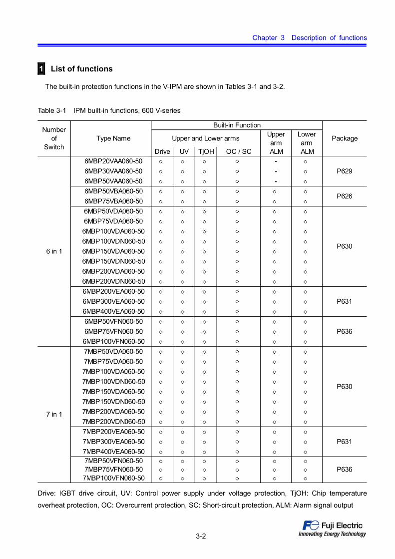
1 List of functions
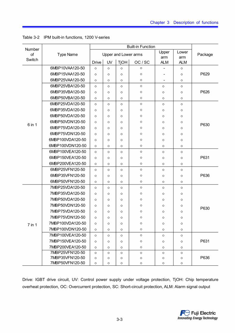
The built-in protection functions in the V-IPM are shown in Tables 3-1 and 3-2.
Table 3-1 IPM built-in functions, 600 V-series
Upperarm
Lowerarm
Drive UV TjOH ALM ALM
- - -
P630
Numberof
Switch
6MBP50VBA060-50
6MBP75VBA060-50
6MBP20VAA060-50
6MBP30VAA060-50
6MBP50VAA060-50
6 in 1
6MBP75VDA060-50
6MBP150VDA060-50
6MBP400VEA060-50
6MBP50VFN060-50
6MBP75VFN060-50
6MBP100VFN060-50
Built-in Function
PackageType Name
6MBP50VDA060-50
P629
P626
Upper and Lower arms
OC / SC
P630
6MBP100VDA060-50
6MBP200VDA060-50
6MBP200VEA060-50
6MBP300VEA060-50
6MBP100VDN060-50
6MBP150VDN060-50
6MBP200VDN060-50
P636
P631
7 in 1
7MBP50VFN060-50
7MBP100VDN060-50
7MBP150VDN060-50
7MBP400VEA060-50
7MBP50VDA060-50
7MBP75VDA060-50
7MBP100VDA060-50
7MBP150VDA060-50
7MBP200VDA060-50
7MBP200VEA060-50
P636
7MBP200VDN060-50
7MBP75VFN060-50 7MBP100VFN060-50
P6317MBP300VEA060-50
Drive: IGBT drive circuit, UV: Control power supply under voltage protection, TjOH: Chip temperature
overheat protection, OC: Overcurrent protection, SC: Short-circuit protection, ALM: Alarm signal output
Chapter 3 Description of functions
3-3
Table 3-2 IPM built-in functions, 1200 V-series
Upperarm
Lowerarm
Drive UV TjOH ALM ALM
- - -
7MBP35VFN120-507MBP50VFN120-50
7 in 1
P636
P636
7MBP75VDN120-50
7MBP100VDN120-50
P630
6 in 1
6MBP25VFN120-50
6MBP35VFN120-50
6MBP50VFN120-50
7MBP25VFN120-50
6MBP50VDN120-50
6MBP75VDN120-50
6MBP100VDN120-50
7MBP50VDN120-50
OC / SC
7MBP100VDA120-50
7MBP75VDA120-50
Numberof
SwitchType Name
7MBP50VDA120-50
7MBP25VDA120-50
7MBP35VDA120-50
6MBP200VEA120-50
6MBP75VDA120-50
6MBP100VDA120-50
6MBP100VEA120-50
6MBP150VEA120-50
Package
7MBP100VEA120-50
7MBP150VEA120-50
7MBP200VEA120-50
6MBP10VAA120-50
6MBP15VAA120-50
6MBP25VAA120-50
Upper and Lower arms
P631
6MBP25VBA120-50
6MBP35VBA120-50
6MBP50VBA120-50
6MBP25VDA120-50
6MBP35VDA120-50
6MBP50VDA120-50
Built-in Function
P626
P631
P629
P630
Drive: IGBT drive circuit, UV: Control power supply under voltage protection, TjOH: Chip temperature
overheat protection, OC: Overcurrent protection, SC: Short-circuit protection, ALM: Alarm signal output
Chapter 3 Description of functions
3-4
N-sidePWM input
P-sidePWM input
Brakeinput
P
B
N
UVW
IPM
Pre-Driver Pre-Driver Pre-Driver
Alarmoutput
Alarmoutput
Alarmoutput
Pre-Driver Pre-Driver Pre-Driver
Alarmoutput
Pre-Driver
2 Description of functions
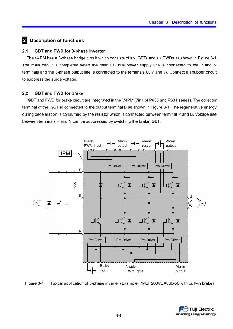
2.1 IGBT and FWD for 3-phase inverter
The V-IPM has a 3-phase bridge circuit which consists of six IGBTs and six FWDs as shown in Figure 3-1.
The main circuit is completed when the main DC bus power supply line is connected to the P and N
terminals and the 3-phase output line is connected to the terminals U, V and W. Connect a snubber circuit
to suppress the surge voltage.
2.2 IGBT and FWD for brake
IGBT and FWD for brake circuit are integrated in the V-IPM (7in1 of P630 and P631 series). The collector
terminal of the IGBT is connected to the output terminal B as shown in Figure 3-1. The regenerative energy
during deceleration is consumed by the resistor which is connected between terminal P and B. Voltage rise
between terminals P and N can be suppressed by switching the brake IGBT.
Figure 3-1 Typical application of 3-phase inverter (Example: 7MBP200VDA060-50 with built-in brake)
Chapter 3 Description of functions
3-5
2.3 IGBT drive function
Figure 3-2 shows a block diagram of the Pre-Driver. The V-IPM has a built-in gate drive circuit for the
IGBT and it is possible to drive the IGBT by inputting an opto-isolated control signal to the V-IPM without
designing the gate resistance value.
The features of this drive function are introduced below:
Independent turn-on and turn-off control
The V-IPM has an independent gate drive circuits for turn-on and turn-off of the IGBT instead of a
single gate resistance. The drive circuits control the dv/dt of turn-on and turn-off independently and
maximize the performance of the device.
Soft shutoff
The gate voltage is gradually reduced at the occasion of the IGBT shutoff when the protection function
is activated in various kinds of abnormal modes. The soft shutoff suppresses the surge voltage during
the turn-off and prevents the breakdown of the device.
Prevention of false turn-on
The gate electrode of the IGBT is connected to the grounded emitter with low impedance. It prevents
false turn-on of the IGBT due to the increase of the VGE due to noise or other cause.
No reverse bias power supply is necessary
The wiring length between the control IC and the IGBT in the V-IPM are short and the wiring
impedance is small, therefore the V-IPM can be driven without reverse bias.
Chapter 3 Description of functions
3-6
Figure 3-2 Pre-Driver block diagram (Example: 7MBP200VDA060-50)
2.4 Protective functions
The V-IPM has protection circuits which prevent failures of the IPM caused by an abnormal mode. The
V-IPM has four kind of protective functions; OC (overcurrent protection), SC (short-circuit protection), UV
(control power supply under voltage protection) and TjOH (chip temperature overheat protection).
When a protective function is activated, the MOSFET for alarm output is turned on and the alarm output
terminal voltage changes from High to Low. The alarm output terminal becomes conductive to GND.
Furthermore, since a 1.3 kΩ resistance is connected in series between the control IC and the alarm output
terminal, an opto-coupler that is connected between the ALM terminal and the Vcc terminal can be driven
directly.
Alarm signal output function
When the protected operation is activated, the IGBT is not turned on even when an ON signal is input.
The failure mode is identified and the IGBT goes through soft shutoff. The alarm signal can be output
from the phase that detected the failure mode individually.
• After the elapse of tALM from the alarm signal output the input signal will be OFF then the protection
operation is stopped and normal operation is restarts.
Chapter 3 Description of functions
3-7
• Even in case the alarm factor is dissolved within the alarm signal output period (tALM), the protected
operation continues during the alarm signal output period (tALM), and accordingly, the IGBT is not
turned on.
Furthermore, the alarm circuits for the lower arm devices including brake circuit are connected
mutually. If protection operation occurs on the lower arm side, all the IGBTs of the lower arms are turned
off during the protection operation.
* P629 package has protective functions on both of the upper arm and the lower arm devices, but the
upper arm devices do not have an alarm signal output function. The lower arm devices have both, the
protective functions and alarm signal output function.
Alarm factor identification function
As the alarm signal output period (tALM) varies in correspondence to the failure mode, the failure mode
can be identified by measuring the alarm signal pulse width.
Alarm factor Alarm signal output period (tALM)
Overcurrent protection (OC)
Short-circuit protection (SC) 2 ms (typ.)
Control power supply under
voltage protection (UV) 4 ms (typ.)
Chip temperature overheat
protection (TjOH) 8 ms (typ.)
However, the pulse width of the alarm signal output through an optocoupler varies by the influence of a
time delay of the optocoupler and other peripheral circuits. It is necessary to take these influences into
account in your design.
Chapter 3 Description of functions
3-8
2.5 Overcurrent protection function: Over Current (OC)
The IGBT’s forward collector current is measured by the current sense IGBT built in the IGBT chip. When
the forward collector current exceeds the protection level (IOC) and continues longer than tdoc (typ. 5 µs), it
is judged as being in the OC status and the IGBT is turned off to prevent occurrence of breakdown by the
overcurrent. At the same time, an alarm signal is provided. The OC status alarm signal period (tALM) is 2 ms.
• Protection operation is stopped and normal operation is restarted if the current level is lower than the IOC
level and the input signal is OFF after 2 ms (tALM) of the alarm signal output.
• Even in case the current level goes back to below the IOC within the 2 ms (tALM), the protection operation
continues until the end of the period of 2 ms (tALM) elapses and accordingly the IGBT is not turned on.
2.6 Short-circuit protective function: Short Circuit (SC)
The SC protective function prevents the IPM form being damaged by the peak current during load
short-circuit and arm short-circuit. When the IGBT’s forward collector current exceeds the protection level
(ISC) and continues longer than tdsc, it is judged as being in the SC status and the protective function is
activated then the IGBT is softly turned off to prevent occurrence of breakdown by short-circuit. At the same
time an alarm signal is output. The SC status alarm signal output period (tALM) is 2 ms.
• Protection operation is stopped and normal operation is resumed if the current level is lower than the ISC
level and the input signal is OFF after 2 ms (tALM) of the alarm signal output.
• Even in case that the short circuit disappears within 2 ms (tALM), the protective operation continues until
the period of 2 ms (tALM) elapses and accordingly the IGBT is not turned on.
2.7 Control power supply under voltage protection function (UV)
The UV protective function prevents malfunction of the control IC caused by a voltage drop of the control
power supply voltage (VCC) and thermal breakdown of the IGBT caused by increase of the VCE (sat) loss.
When VCC is continuously below the voltage protection trip level (VUV) for a period of 20 µs, it is judged as
being in the UV status and the IGBTs are softly turned off to prevent malfunction and breakdown caused by
the control power supply voltage drop. When it is judged as being in the UV status, the protective function is
activated and the alarm signal is generated. The alarm signal output period (tALM) of the UV protection is 4
ms.
Chapter 3 Description of functions
3-9
• As hysteresis VH is provided, protection operation is stopped and normal operation is resumed, if VCC is
higher than (VUV + VH) and the input signal is OFF. A 4 ms (tALM) alarm signal will be send to the output
• Even in case the supply voltage exceeds (VUV + VH) within 4 ms (tALM), the protective operation continues
until the period of 4 ms (tALM) elapses, and accordingly, the IGBT is not turned on.
Furthermore, an alarm signal for judgment of the UV status is provided at the time of startup and
shutdown of the control power supply.
2.8 Chip temperature overheat protective function: IGBT chip Over Heat protection (TjOH)
The TjOH protective function includes the direct IGBT chip temperature detected by a built-in on-chip
temperature sensor on each IGBT chip. If the IGBT chip temperature is continuously higher than protection
trip level (TjOH) for 1.0 ms, it is judged as being in the overheat status, the TjOH protective function is
activated then the IGBTs are softly turned off to prevent a failure of the IGBT. At the same time an alarm
signal output is generated. The UV status alarm signal output period (tALM) is 8 ms.
• There is a hysteresis offset TjH, the protective operation is stopped and normal operation is resumed, if Tj
is below (TjOH – TjH) and the input signal is OFF after 8 ms (tALM) of the alarm signal output.
• Even in case the alarm signal disappears within 8 ms (tALM), the protected operation continues until the
period of 8 ms (tALM) elapses, and accordingly, the IGBT is not turned on.
A case temperature overheat protective function (TCOH), which is built in the former IPM series, is not
built in the V-IPM series. The IGBT chip overheat status is protected by the TjOH protective function.

Chapter 3 Description of functions
3-10
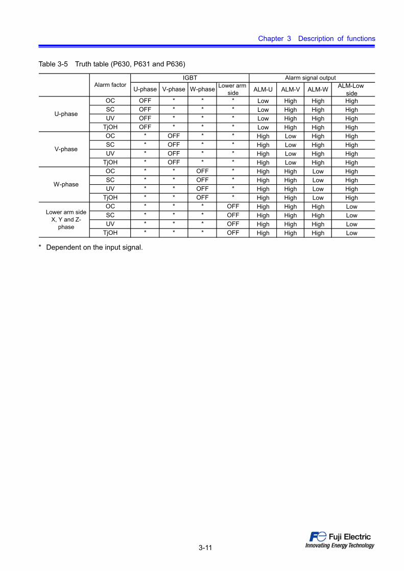
3 Truth table
The truth tables of the V-IPM series when protective function is activated are shown in Tables 3-3 to 3-5.
Table 3-3 Truth table (P629)
Alarm signal output
ALM-Low side
High
High
High
High
High
High
High
High
High
High
High
High
Low
Low
Low
Low
*
TjOH
IGBT
W-phaseV-phase
*
*
*
Lower arm side
*
OC
OC
*
UV
SC OFF
OFF
Alarm factor
*
* *
U-phase
OFF
OFF
* *
UV *
OC
TjOH
*
*
*
OC
UV
*
TjOH *
*
*
*
TjOH
UV
*SC
*
OFF *
*
*
*
* OFF *
OFF *
* * OFF
* * OFF
* * OFF
*
OFF**
*
*OFF
*
*OFFSC
* OFF *
* OFF
*
SC * OFF *
Lower arm side
X, Y and Z-phase
W-phase
V-phase
U-phase
* Dependent on the input signal.
Table 3-4 Truth table (P626)
ALM-U ALM-V ALM-WALM-Low
sideLow High High High
Low High High High
Low High High High
Low High High High
High Low High High
High Low High High
High Low High High
High Low High High
High High Low High
High High Low High
High High Low High
High High Low High
High High High Low
High High High Low
High High High Low
High High High Low
* *
*OFF*
OFF *
* OFF
SC
***OFFSC
**OFF*
Lower arm side
X, Y and Z-phase
W-phase
V-phase
U-phase
* *
OC
OC
TjOH
* *
OFF *
UV
Alarm signal output
* *
V-phase
*
*
*
OFF
*
IGBT
W-phaseLower arm
side* *
*
Alarm factorU-phase
OFF
OFF
OFF
UV *
OC
TjOH
*
*
*
SC
*
*
*
OC
UV
TjOH
UV
*
SC *
TjOH *
*
* OFF *
OFF *
*
*
* * OFF
* * OFF
* * OFF
OFF
* Dependent on the input signal.
Chapter 3 Description of functions
3-11
Table 3-5 Truth table (P630, P631 and P636)
ALM-U ALM-V ALM-WALM-Low
sideLow High High High
Low High High High
Low High High High
Low High High High
High Low High High
High Low High High
High Low High High
High Low High High
High High Low High
High High Low High
High High Low High
High High Low High
High High High Low
High High High Low
High High High Low
High High High Low
* *
*OFF*
OFF *
* OFF
SC
***OFFSC
**OFF*
Lower arm sideX, Y and Z-
phase
W-phase
V-phase
U-phase
* *
OC
OC
TjOH
* *
OFF *
UV
Alarm signal output
* *
V-phase
*
*
*
OFF
*
IGBT
W-phaseLower arm
side* *
*
Alarm factorU-phase
OFF
OFF
OFF
UV *
OC
TjOH
*
*
*
SC
*
*
*
OC
UV
TjOH
UV
*
SC *
TjOH *
*
* OFF *
OFF *
*
*
* * OFF
* * OFF
* * OFF
OFF
* Dependent on the input signal.
Chapter 3 Description of functions
3-12
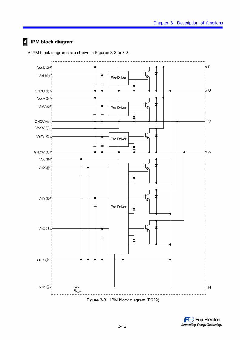
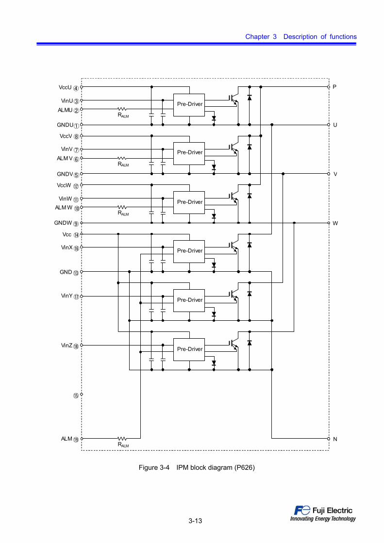
4 IPM block diagram
V-IPM block diagrams are shown in Figures 3-3 to 3-8.
Figure 3-3 IPM block diagram (P629)
U
V
W
Vcc ⑪
VinX ⑫
VinY ⑬
VinZ ⑭
ALM ⑮
VccV ⑥
GNDV ④
PVccU ③
GNDU ①
VinU ②
VinV ⑤
VccW ⑨
GNDW ⑦
VinW ⑧
GND ⑩
N
Pre-Driver
Pre-Driver
Pre-Driver
Pre-Driver
RALM
Chapter 3 Description of functions
3-13
Figure 3-4 IPM block diagram (P626)
Vcc ⑭
VinX ⑯
GND ⑬
VinY ⑰
VinZ⑱
ALM ⑲
VccV ⑧
GNDV⑤
VccU ④
GNDU①
VinU③
VinV ⑦
VccW ⑫
GNDW ⑨
VinW ⑪
⑮
ALMU ②
ALM V ⑥
ALM W ⑩
Pre-Driver
Pre-Driver
Pre-Driver
Pre-Driver
Pre-Driver
Pre-Driver
RALM
RALM
RALM
RALM
U
V
W
P
N
Chapter 3 Description of functions
3-14
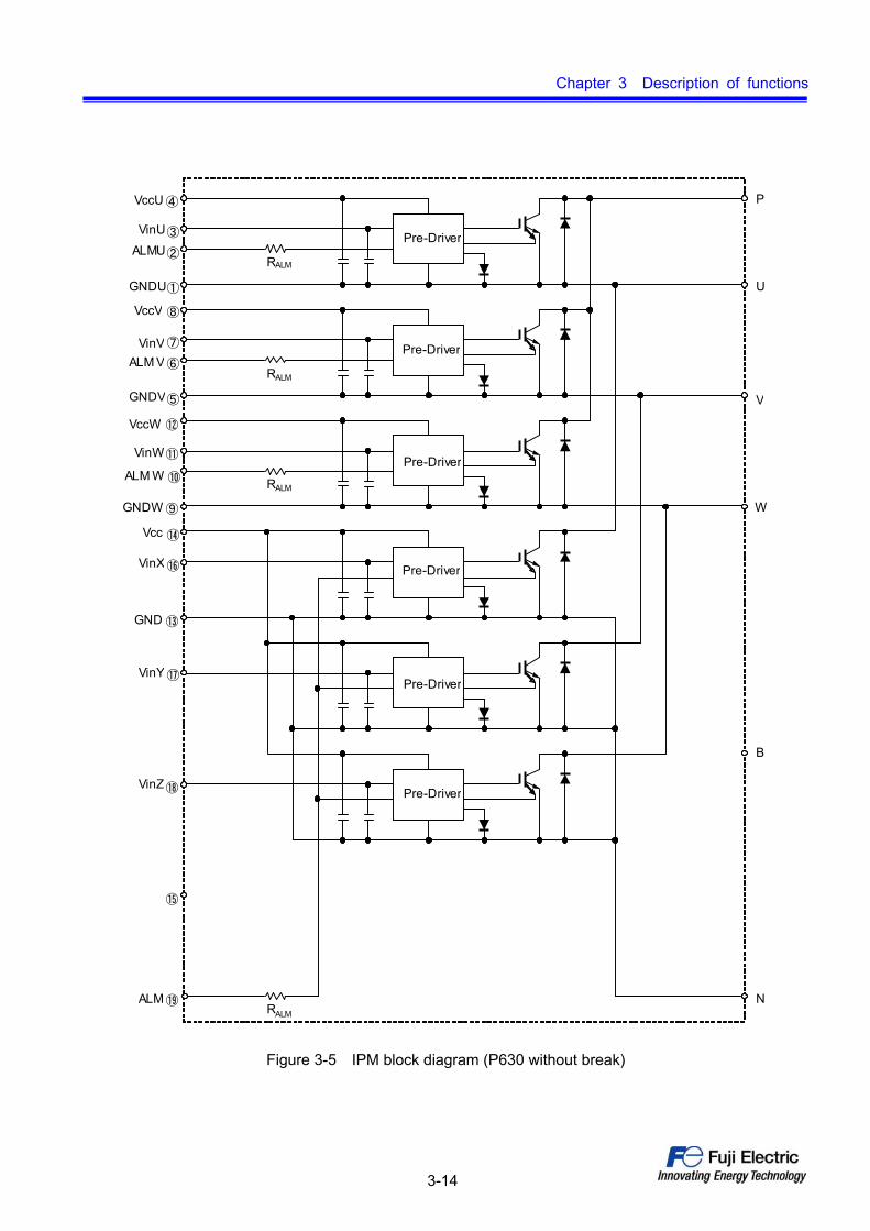
Figure 3-5 IPM block diagram (P630 without break)
Vcc ⑭
VinX ⑯
GND ⑬
VinY ⑰
VinZ⑱
ALM ⑲
VccV ⑧
GNDV⑤
VccU ④
GNDU①
VinU③
VinV ⑦
VccW ⑫
GNDW ⑨
VinW⑪
⑮
ALMU②
ALM V ⑥
ALM W ⑩
Pre-Driver
Pre-Driver
Pre-Driver
Pre-Driver
Pre-Driver
Pre-Driver
RALM
RALM
RALM
RALM
U
V
W
P
N
B
Chapter 3 Description of functions
3-15
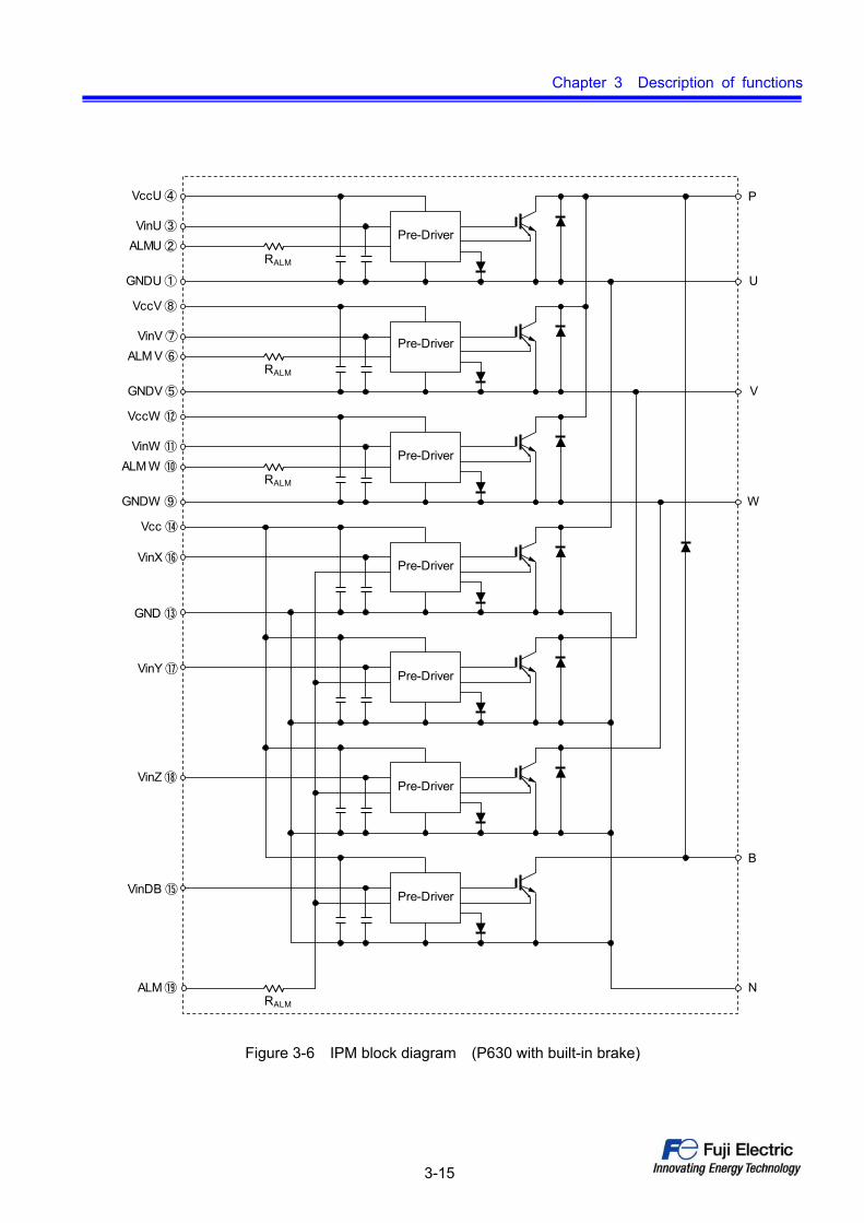
Figure 3-6 IPM block diagram (P630 with built-in brake)
Pre-Driver
Pre-Driver
Pre-Driver
Pre-Driver
Pre-Driver
Pre-Driver
RALM
RALM
RALM
Pre-Driver
RALM
Vcc ⑭
VinX ⑯
GND ⑬
VinY ⑰
VinZ ⑱
ALM ⑲
B
VccV ⑧
GNDV ⑤
VccU ④
GNDU ①
VinU ③
VinV ⑦
VccW ⑫
GNDW ⑨
VinW ⑪
VinDB ⑮
ALMU ②
ALM V ⑥
ALM W ⑩
U
V
W
P
N
Chapter 3 Description of functions
3-16
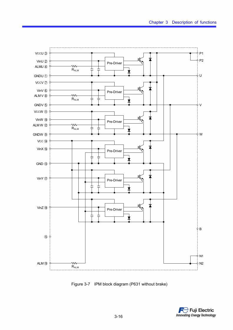
Figure 3-7 IPM block diagram (P631 without brake)
VCC ⑭
VinX ⑯
GND ⑬
VinY ⑰
VinZ ⑱
ALM ⑲
VCCV ⑦
GNDV ⑤
VCCU ③
GNDU ①
VinU ②
VinV ⑥
VCCW ⑪
GNDW ⑨
VinW ⑩
⑮
ALMU ④
ALM V ⑧
ALM W ⑫
Pre-Driver
Pre-Driver
Pre-Driver
Pre-Driver
Pre-Driver
Pre-Driver
RALM
RALM
RALM
RALM
U
V
W
P1
P2
N1
N2
B
Chapter 3 Description of functions
3-17
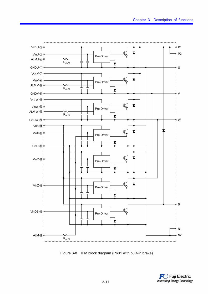
Figure 3-8 IPM block diagram (P631 with built-in brake)
Pre-Driver
Pre-Driver
Pre-Driver
Pre-Driver
Pre-Driver
Pre-Driver
RALM
RALM
RALM
Pre-Driver
RALM
VCC ⑭
VinX ⑯
GND ⑬
VinY ⑰
VinZ ⑱
ALM ⑲
B
VCCV ⑦
GNDV ⑤
VCCU ③
GNDU ①
VinU ②
VinV ⑥
VCCW ⑪
GNDW ⑨
VinW ⑩
VinDB ⑮
ALMU ④
ALM V ⑧
ALM W ⑫
U
V
W
P1
N2
P2
N1
Chapter 3 Description of functions
3-18
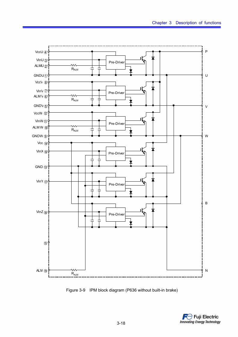
Figure 3-9 IPM block diagram (P636 without built-in brake)
Vcc ⑭
VinX ⑯
GND ⑬
VinY ⑰
VinZ⑱
ALM ⑲
VccV ⑧
GNDV⑤
VccU ④
GNDU①
VinU③
VinV ⑦
VccW ⑫
GNDW ⑨
VinW⑪
⑮
ALMU②
ALM V ⑥
ALM W ⑩
Pre-Driver
Pre-Driver
Pre-Driver
Pre-Driver
Pre-Driver
Pre-Driver
RALM
RALM
RALM
RALM
U
V
W
P
N
B
Chapter 3 Description of functions
3-19
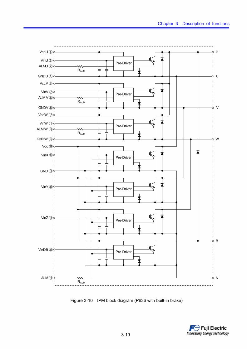
Figure 3-10 IPM block diagram (P636 with built-in brake)
Pre-Driver
Pre-Driver
Pre-Driver
Pre-Driver
Pre-Driver
Pre-Driver
RALM
RALM
RALM
Pre-Driver
RALM
Vcc ⑭
VinX ⑯
GND ⑬
VinY ⑰
VinZ ⑱
ALM ⑲
B
VccV ⑧
GNDV ⑤
VccU ④
GNDU ①
VinU ③
VinV ⑦
VccW ⑫
GNDW ⑨
VinW ⑪
VinDB ⑮
ALMU ②
ALM V ⑥
ALM W ⑩
U
V
W
P
N
Chapter 3 Description of functions
3-20
5 Timing chart
5.1 Control power supply under voltage protection (UV): Case 1
VCC
VUV+VHVUV
5 V
(1) (2) (3) (4)
tALM (UV) tALM (UV)
(5) (6) (7) (8)
Vin
IC
VALM 20 μs 20 μs
tALM (UV)
20 μs
20 μs
High (OFF)
Low (ON)
*1: tALM (UV) is 4 ms, typical.*2: Dead time 20 μs is a typical
20 μs > 20 μs >
< tALM (UV)
High
Low
Protectedperation
In operation
Cancelled
* 1
* 2
(1) At the period of the VCC ramp-up, alarm output begins when the VCC exceeds 5 V and less than VUV.
(See 5.3 for details.)
(2) Protective function is not activated if the length of time during which VCC is lower than VUV is shorter
than 20 µs. (While Vin is off)
(3) While Vin is off, an alarm is generated 20 µs after the VCC drop below VUV, and the IGBT is kept in the
off status.
(4) UV protected operation continues during the tALM (UV) period even if the VCC returns to over (VUV + VH)
and Vin is off. Normal operation is restarted from protected operation after the elapse of the tALM (UV)
period.
(5) Protection operation is not activated if the length of time during which VCC is lower than VUV is shorter
Chapter 3 Description of functions
3-21
than 20 µs. (While Vin is on)
(6) While Vin is on, an alarm output signal is generated 20 µs after VCC drops below VUV , and the IGBT is
softly turned off.
(7) In case VCC returns to over VUV + VH before the elapse of tALM (UV) period and Vin remains on state, an
alarm is output during the tALM (UV) period, but the protective function continues operating until Vin is
changed to off-state.
(8) An alarm output is generated when VCC is below VUV during shutoff. (See 5.3 for details.)
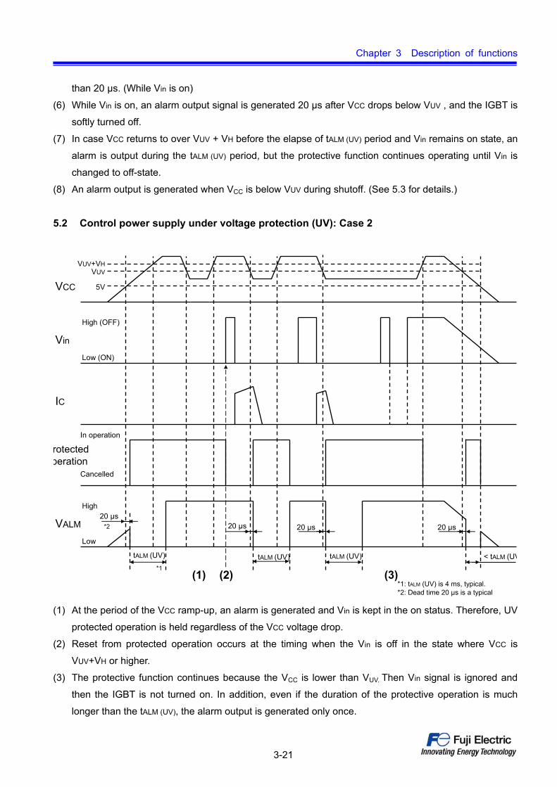
5.2 Control power supply under voltage protection (UV): Case 2
VCC
VUV+VHVUV
5V
tALM (UV) tALM (UV)
Vin
IC
VALM 20 μs 20 μs
tALM (UV)
20 μs
High (OFF)
Low (ON)
20 μs
< tALM (UV
High
Low
*1
*2
rotectedperation
In operation
Cancelled
*1: tALM (UV) is 4 ms, typical.*2: Dead time 20 μs is a typical
(3)(1) (2)
(1) At the period of the VCC ramp-up, an alarm is generated and Vin is kept in the on status. Therefore, UV
protected operation is held regardless of the VCC voltage drop.
(2) Reset from protected operation occurs at the timing when the Vin is off in the state where VCC is
VUV+VH or higher.
(3) The protective function continues because the VCC is lower than VUV. Then Vin signal is ignored and
then the IGBT is not turned on. In addition, even if the duration of the protective operation is much
longer than the tALM (UV), the alarm output is generated only once.

Chapter 3 Description of functions
3-22
5.3 Control power supply under voltage protection (UV) during startup and shutdown of
power supply
V-IPM has control power supply under voltage protection (UV) function. Because of this function, an
alarm output is generated during the startup and shutdown of the power supply. Its details are described
below:
5.3.1 During start up
When VCC exceeds 5 V, an alarm output is
generated after the elapse of 20 μs in both of
Case 1 and Case 2. In Case 1, the VCC
voltage reaches (VUV + VH) and the Vin
becomes off-state within the tALM(UV) and the
protective operation is stopped after the
elapse of tALM (UV). In Case 2, protective
operation continues even after the elapse of
tALM(UV) because the VCC is still below
(VUV+VH). The protected operation is
stopped when VCC exceeds VUV + VH and
Vin is off-state.
5.3.2 During Shutdown
When the VCC becomes less than the
VUV, an alarm signal is generated after
the elapse of 20 μs in both of Case 3
and Case 4. In Case 3, the alarm is
stopped before the tALM(UV) because
the VCC becomes less than 5V before
the elapse of the tALM (UV) and the IPM
operation becomes unstable. In Case 4,
protected operation continues after the
elapse of the tALM(UV) because the VCC is
still higher than 5 V. When the VCC
becomes less than 5 V, the protected
operation of the control IC is stopped
and the VALM changes to VCC
equivalent.
VCC
VUV+VVUV
5V
Case 1
Vin
VALM
tALM (UV)
20 μs
High (OFF)
Low (ON)
VCC
VUV+VHVUV
5V
Case 2
Vin
VALM
tALM (UV)
20 μs
High (OFF)
Low (ON)
High
Low
High
Low
Protected operation
In operation
Cancelled
Protected operation
In operation
Cancelled
VCC
VUV+VHVUV
5V
Vin
VALM
< tALM (UV)
20 μs
High (OFF)
Low (ON)
VCC
VUV+VHVUV
5V
Vin
VALM
tALM (UV)
20 μs
High (OFF)
Low (ON)
High
Low
High
Low
Case 3 Case 4
Protected operation
In operation
Cancelled
Protected operation
In operation
Cancelled
Chapter 3 Description of functions
3-23
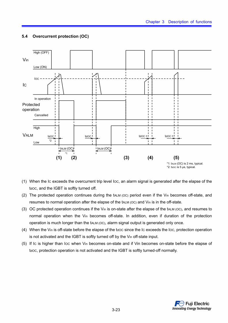
5.4 Overcurrent protection (OC)
Vin
IC
VALM
tALM (OC)
tdOC
tALM (OC)
tdOC tdOC >
IOC
Low (ON)
High (OFF)
High
Low
*1
*2
tdOC >
Protectedoperation
In operation
Cancelled
(1) (2) (3) (4) (5)*1: tALM (OC) is 2 ms, typical.*2: tdOC is 5 μs, typical.
(1) When the IC exceeds the overcurrent trip level IOC, an alarm signal is generated after the elapse of the
tdOC, and the IGBT is softly turned off.
(2) The protected operation continues during the tALM (OC) period even if the Vin becomes off-state, and
resumes to normal operation after the elapse of the tALM (OC) and Vin is in the off-state.
(3) OC protected operation continues if the Vin is on-state after the elapse of the tALM (OC), and resumes to
normal operation when the Vin becomes off-state. In addition, even if duration of the protection
operation is much longer than the tALM (OC), alarm signal output is generated only once.
(4) When the Vin is off-state before the elapse of the tdOC since the IC exceeds the IOC, protection operation
is not activated and the IGBT is softly turned off by the Vin off-state input.
(5) If IC is higher than IOC when Vin becomes on-state and if Vin becomes on-state before the elapse of
tdOC, protection operation is not activated and the IGBT is softly turned-off normally.
Chapter 3 Description of functions
3-24
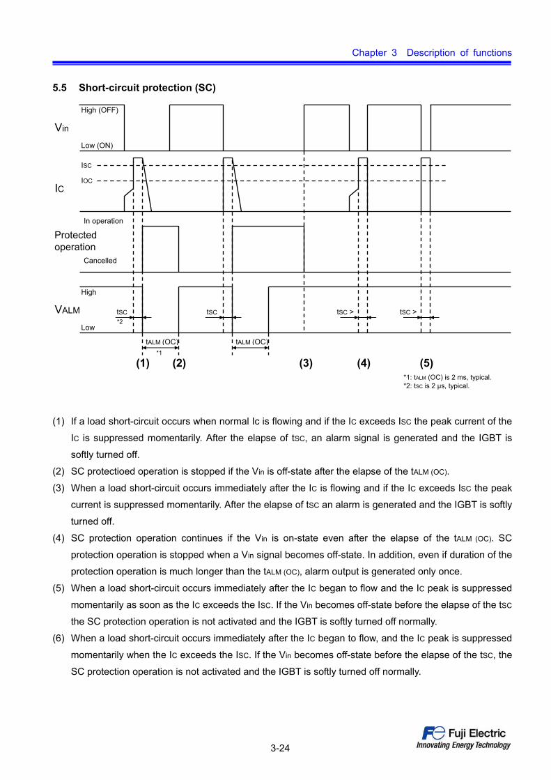
5.5 Short-circuit protection (SC)
Vin
IC
VALM
tALM (OC)
tSC
tALM (OC)
tSC tSC > tSC >
ISC
IOC
Low (ON)
High (OFF)
High
Low
*1
*2
Protectedoperation
In operation
Cancelled
(1) (2) (3) (4) (5)*1: tALM (OC) is 2 ms, typical.*2: tSC is 2 μs, typical.
(1) If a load short-circuit occurs when normal Ic is flowing and if the IC exceeds ISC the peak current of the
IC is suppressed momentarily. After the elapse of tSC, an alarm signal is generated and the IGBT is
softly turned off.
(2) SC protectioed operation is stopped if the Vin is off-state after the elapse of the tALM (OC).
(3) When a load short-circuit occurs immediately after the IC is flowing and if the IC exceeds ISC the peak
current is suppressed momentarily. After the elapse of tSC an alarm is generated and the IGBT is softly
turned off.
(4) SC protection operation continues if the Vin is on-state even after the elapse of the tALM (OC). SC
protection operation is stopped when a Vin signal becomes off-state. In addition, even if duration of the
protection operation is much longer than the tALM (OC), alarm output is generated only once.
(5) When a load short-circuit occurs immediately after the IC began to flow and the IC peak is suppressed
momentarily as soon as the IC exceeds the ISC. If the Vin becomes off-state before the elapse of the tSC
the SC protection operation is not activated and the IGBT is softly turned off normally.
(6) When a load short-circuit occurs immediately after the IC began to flow, and the IC peak is suppressed
momentarily when the IC exceeds the ISC. If the Vin becomes off-state before the elapse of the tSC, the
SC protection operation is not activated and the IGBT is softly turned off normally.
Chapter 3 Description of functions
3-25
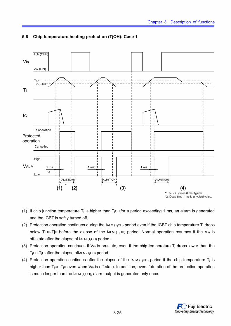
5.6 Chip temperature heating protection (TjOH): Case 1
Vin
IC
VALM
tALM(TjOH)
1 ms
TjOHTjOH-TjH
tALM(TjOH)
1 ms
Tj
Low (ON)
High (OFF)
High
Low
tALM(TjOH)
1 ms
*2
*1
Protectedoperation
In operation
Cancelled
(1) (2) (3) (4)*1: tALM (TjOH) is 8 ms, typical.*2: Dead time 1 ms is a typical value.
(1) If chip junction temperature Tj is higher than TjOH for a period exceeding 1 ms, an alarm is generated
and the IGBT is softly turned off.
(2) Protection operation continues during the tALM (TjOH) period even if the IGBT chip temperature Tj drops
below TjOH-TjH before the elapse of the tALM (TjOH) period. Normal operation resumes if the Vin is
off-state after the elapse of tALM (TjOH) period.
(3) Protection operation continues if Vin is on-state, even if the chip temperature Tj drops lower than the
TjOH-TjH after the elapse oftALM (TjOH) period.
(4) Protection operation continues after the elapse of the tALM (TjOH) period if the chip temperature Tj is
higher than TjOH-TjH even when Vin is off-state. In addition, even if duration of the protection operation
is much longer than the tALM (TjOH), alarm output is generated only once.
Chapter 3 Description of functions
3-26
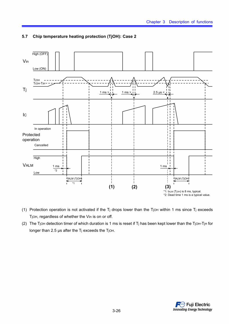
5.7 Chip temperature heating protection (TjOH): Case 2
2.5 μs <1 ms >1 ms >
Vin
IC
VALM
tALM (TjOH)
1 ms
TjOHTjOH-TjH
tALM (TjOH)
1 ms
Tj
Low (ON)
High (OFF)
High
Low*2
Protectedoperation
In operation
Cancelled
(1) (2) (3)*1: tALM (TjOH) is 8 ms, typical.*2: Dead time 1 ms is a typical value.
*1
(1) Protection operation is not activated if the Tj drops lower than the TjOH within 1 ms since Tj exceeds
TjOH, regardless of whether the Vin is on or off.
(2) The TjOH detection timer of which duration is 1 ms is reset if Tj has been kept lower than the TjOH-TjH for
longer than 2.5 µs after the Tj exceeds the TjOH.
Chapter 3 Description of functions
3-27
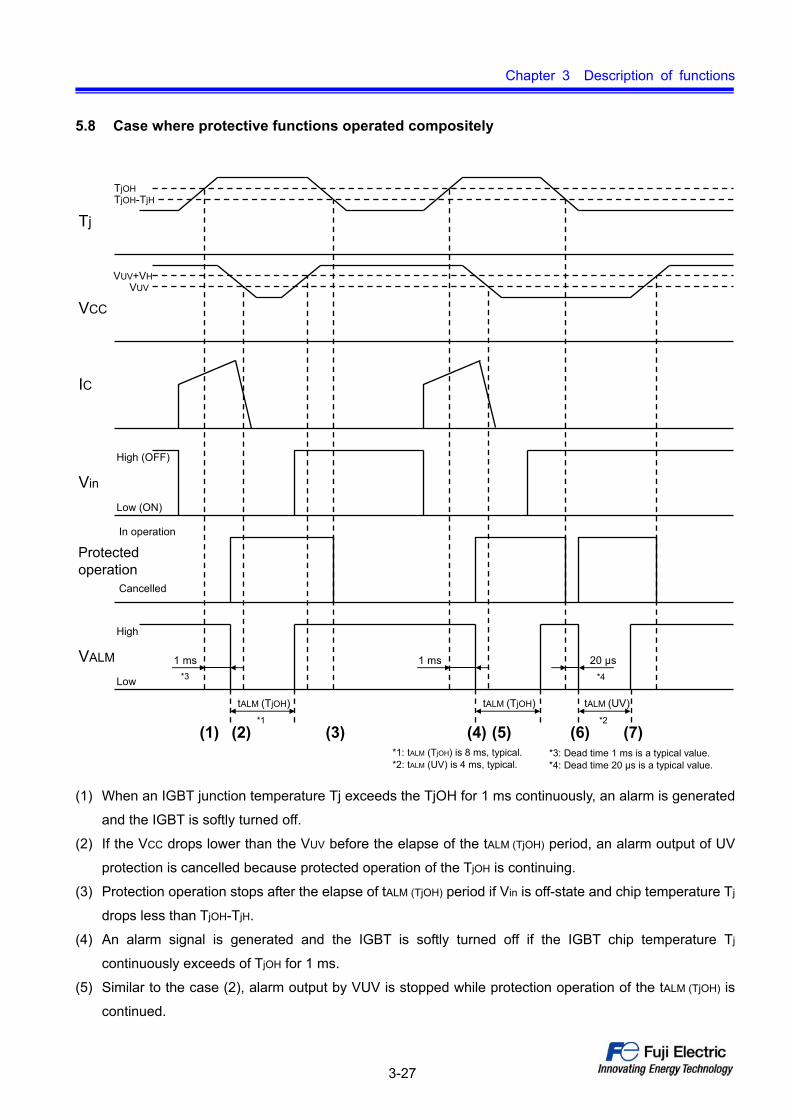
5.8 Case where protective functions operated compositely
VCC
VUV+VHVUV
VALM
tALM (UV)
High
Low
Vin
High (OFF)
Low (ON)
20 μs1 ms
tALM (TjOH)
TjOHTjOH-TjH
Tj
1 ms
tALM (TjOH)
IC
*3
Protectedoperation
In operation
Cancelled
*1 *2
(1) (2) (3) (4) (5) (6) (7)*1: tALM (TjOH) is 8 ms, typical.*2: tALM (UV) is 4 ms, typical.
*3: Dead time 1 ms is a typical value.*4: Dead time 20 μs is a typical value.
*4
(1) When an IGBT junction temperature Tj exceeds the TjOH for 1 ms continuously, an alarm is generated
and the IGBT is softly turned off.
(2) If the VCC drops lower than the VUV before the elapse of the tALM (TjOH) period, an alarm output of UV
protection is cancelled because protected operation of the TjOH is continuing.
(3) Protection operation stops after the elapse of tALM (TjOH) period if Vin is off-state and chip temperature Tj
drops less than TjOH-TjH.
(4) An alarm signal is generated and the IGBT is softly turned off if the IGBT chip temperature Tj
continuously exceeds of TjOH for 1 ms.
(5) Similar to the case (2), alarm output by VUV is stopped while protection operation of the tALM (TjOH) is
continued.
Chapter 3 Description of functions
3-28
(6) Protected operation stops after the elapse of tALM (TjOH) period if Vin is off-state and the chip
temperature Tj drops lower than the TjOH-TjH. At this time VCC is kept lower than the VUV for 20 µs after
the stop of protective functions by TjOH, an alarm is generated by the VUV again and the UV protected
operation is activated.
(7) Protected operation stops after the elapse of tALM (UV) period if Vin is off-state and VCC is higher than
VUV + VH.
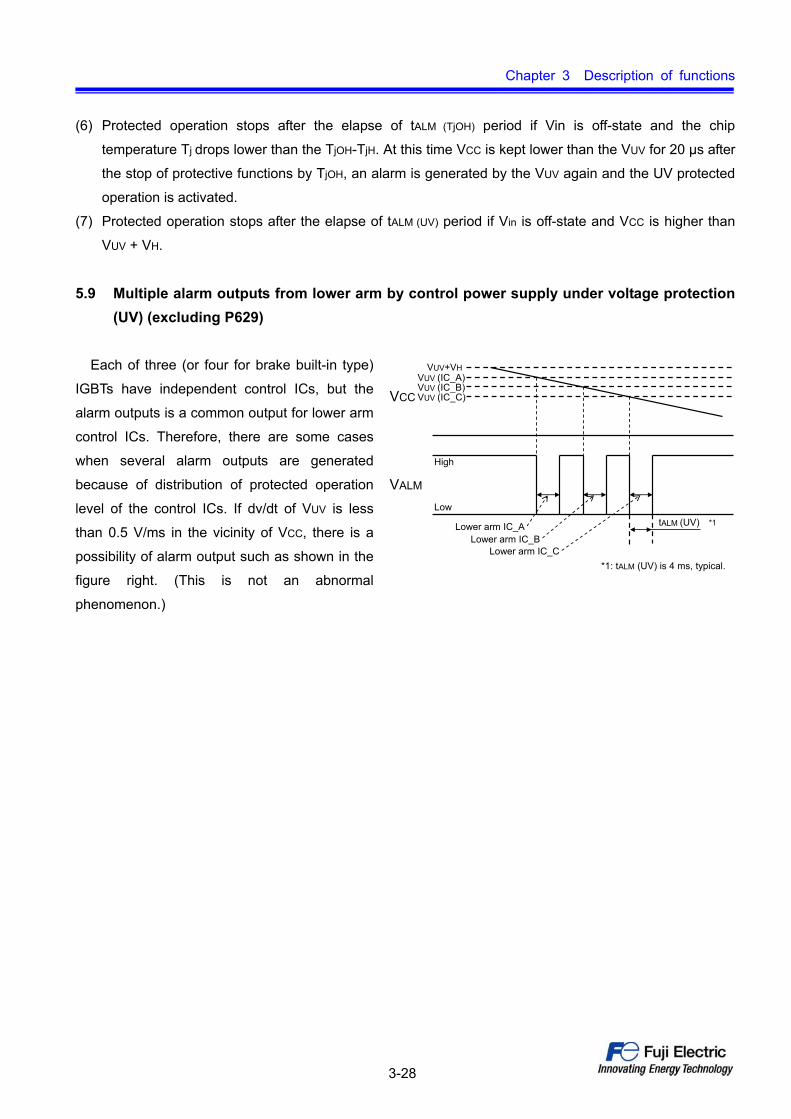
5.9 Multiple alarm outputs from lower arm by control power supply under voltage protection
(UV) (excluding P629)
Each of three (or four for brake built-in type)
IGBTs have independent control ICs, but the
alarm outputs is a common output for lower arm
control ICs. Therefore, there are some cases
when several alarm outputs are generated
because of distribution of protected operation
level of the control ICs. If dv/dt of VUV is less
than 0.5 V/ms in the vicinity of VCC, there is a
possibility of alarm output such as shown in the
figure right. (This is not an abnormal
phenomenon.)
VCC
VUV+VHVUV (IC_A)
VALM
*1: tALM (UV) is 4 ms, typical.
High
Low
Lower arm IC_ALower arm IC_B
Lower arm IC_C
tALM (UV) *1
VUV (IC_B)VUV (IC_C)