closed-loop gate drive for high power igbts -...
TRANSCRIPT
Closed-Loop Gate Drive for High Power IGBTs
Lihua Chen and Fang Z. Peng Michigan State University
2120 Engineering Building
East Lasing, MI 48824 USA
Abstract-To overcome the drawbacks of the conventional gate
drive, in this paper a closed-loop gate control method is proposed.
In this novel method, the switching speed, specifically di/dt, is
measured from the voltage across the parasitic inductance of the
IGBT module and a closed-loop control is employed to adaptively
adjust the gate drive voltage to control the switching speed
according to a preset control reference. As a result, both the
voltage overshoot and current overshoot can be effectively
controlled. This new gate drive method enables programmable
control of switching speed and allows full use of the capability of
the power devices. The oscillations during IGBT switching are
also reduced and associated EMI problems can be mitigated. The
relationships between the controlled voltage overshoot, current
overshoot and associated energy losses are derived and can
provide guidelines for practical design. Also, the proposed gate
drive fully utilizes gate drive signal information of amplitude and
duty cycle, and provides a new capability for the system
modulator to effectively control both the power electronic
circuit’s steady-state and transient behaviors simultaneously.
I. INTRODUCTION
Based on the IGBT switching transient analysis [1], it was
found that there exist two major issues during the switching of
IGBTs. 1. during the IGBT turn-on, there occurs a current
overshoot caused by the fast snap-off of the freewheeling diode
(FWD). 2. during the IGBT turn-off, there occurs a voltage
overshoot caused by the fast turn-off of the IGBT and parasitic
inductances. Other problems associated with the switching of
the IGBTs, like ringing, EMI, etc. are derived from these two
major issues.
The research on the gate drive circuit for the IGBT started
almost as early as the application of this type of semiconductor
device [2]. Much work has been done and focused on open-
loop gate control to improve the transient performance of the
IGBT [3]-[15]. In summary, most solutions were limited to
empirical tests and discussion of the results. However,
conventional gate drive methods cannot solve these two
problems without compromising with lengthened delays, low
noise immunity, and high switching energy losses. A closed-
loop active gate drive concept to control the switching transient
of the IGBT has been introduced to reduce EMI by providing
less rapid switching [16]. Also an active voltage ramp control
for IGBTs has only been implemented with traditional closed-
loop methods for the applications which have IGBTs
connected in series [17]-[24]. However, the large power loss
associated with the slow voltage rise ramp is usually
unacceptable in real applications.
To overcome the drawbacks of the conventional gate drive,
in this work, a novel closed-loop gate drive method featuring
active control of switching speed for high power IGBTs is
proposed. To achieve this control, the switching speed,
specifically di/dt, is derived from a measurement of the voltage
across the parasitic inductance of the IGBT module and a
closed-loop control is employed to adaptively adjust the
switching speed according to preset references. As a result,
both the voltage overshoot and current overshoot can be
effectively controlled. In the following discussion, the
principle of the proposed gate drive method is explained in
detail and experimental results are provided to justify the
validity and features of the proposed novel method. The
advantages associated with this new method are summarized in
the conclusion section.
II. PROPOSED CLOSED-LOOP GATE CONTROL
To achieve bidirectional current flow, an IGBT module is
actually configured with an IGBT and an anti-parallel power
diode. The power diode's dynamic behaviors impact
significantly the IGBT switching transient. The analysis of the
dynamic characteristics of power diodes reveals that the peak
reverse recovery current, Irr, is proportional to the rate of
change of the reverse-recovery current, diR/dt. And this
relationship can be approximately explained in (1) [1].
62.8 10 /BD F RI BV I di dtrr−
≈ × (1)
where IF is diode forward current, BVBD is diode breakdown
voltage. It should be pointed that during the snap-off of the
anti-parallel diode, the diR/dt is the same as the rate of change
of the opposite IGBT collector current, diC/dt.
During the turn-off of the IGBT, the voltage overshoot, Vos,
is also proportional to the rate of change of the IGBT collector
current and this relationship can be explained in (2).
dtdi
LV CSOS = (2)
where LS is the stray inductance of power electronic circuit.
Equations (1) and (2) indicate that the control of the diC/dt of
the IGBT can directly control the current overshoot during
IGBT turn-on, and control the voltage overshoot during IGBT
turn-off. The flexible controllability of modern IGBTs enables
the control of the diC/dt via gate drive methods [25], and these
relationships can be described as follows.
978-1-422-2812-0/09/$25.00 ©2009 IEEE 1331
During IGBT turn-on the diC/dt is expressed as:
( / 2 )
11
GG T
S
V V I gdi p mc
dt R Cg iesL
gm
− −
=
+
(3)
During IGBT turn-off the diC/dt is expressed as:
( / 2 )
1
T L GG
S
di V I g Vc m
dt R Cg iesL
gm
+ −=
+
(4)
Where VGG is gate drive voltage; IL is load current; gm is IGBT
transconductance; Rg is gate drive resistance; Cies is IGBT
input parasitic capacitance; VT is IGBT threshold voltage, LS1 is
the stray inductance between the IGBT chip emitter and the
Kelvin emitter. Within the two parts in the denominator on the
right side of (3) and (4), although LS1 is usually very small, it is
still comparable to the other component of the denominator,
since the transconductance, gm, has a large value for high
power IGBTs. With the conventional gate drive methods, the
amount of control over the di/dt obtained by changing the gate
resistance, Rg, is very limited because this effect is attenuated
by a large value of gm.
Unlike the conventional methods, in the proposed closed-
loop gate drive, by adaptively varying the gate drive voltage,
VGG, shown in the numerator of (3) and (4), the gate drive can
control the IGBT switching speed, specifically di/dt, and
therefore the current overshoot and voltage overshoot across
the IGBT.
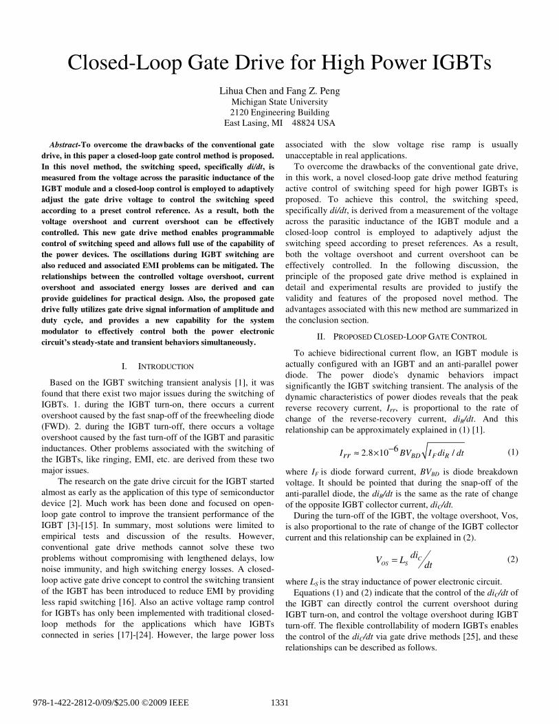
Fig. 1 shows the schematic of the proposed closed-loop gate
drive. For the on-state and off-state control of the IGBT, the
positive inputs of the Op Amps, OP1 and OP2, are zero volts,
and the control input signal is amplified by OP1, OP2 and a
power stage. The IGBT gate voltage is firmly clamped to either
turn-on voltage VCC, in most applications +15V, or turn-off
voltage VEE, usually -8V to -15V. This leads to stable on and
off states for the IGBT.
Fig. 1. Proposed close-loop gate drive circuit.
During the IGBT turn-on and turn-off transients, a
substantial voltage appears across the parasitic inductance, LEe
(shown with a dotted line in Fig. 1), of the main emitter and
Kelvin emitter of the IGBT module. This voltage is linearly
proportional to the rate of change of the IGBT collector current,
diC/dt, specifically expressed as:
dtdi
LV CEeEe = (5)
Also, as shown in (2), this voltage is linearly proportional to
the voltage overshoot. The voltage is measured and adjusted by
Op Amp OP3, and fed to the positive input of OP1. During the
switching transient, the error between the control input voltage
and the measured voltage overshoot is amplified and used to
adaptively adjust the IGBT gate drive voltage, VGG. As
expressed in (3) and (4), the IGBT switching speed can be
actively manipulated, and hence the current overshoot and
voltage overshoot can be controlled by varying the control
input voltage reference, Vref1 and Vref2. Specifically, change
the amplitude of Vref1 to control the turn-on switching speed
and change the amplitude of Vref2 to control the turn-off
switching speed.
To overcome the latency behavior of the IGBT and improve
the stability of the closed-loop control, a phase-lead
compensation is implemented by measuring the derivative of
the collector voltage with the capacitor C1 and resistor R1, and
feeding this to the positive input of OP2. This compensation
should be kept as small as possible to avoid dramatically
slowing down the rate of change of the IGBT collector voltage,
dv/dt, since a slow voltage ramp causes additional energy loss,
which is not desired in real applications. Also, theoretically
there are no relationship between the dv/dt and current
overshoot and voltage overshoot. It was also found that the
gain of OP2 should be kept small to improve noise immunity
and avoid oscillations. In the hardware implementation,
optimized results were achieved when the gain of OP2 was set
to two by the ratio of the resistances of R6 over R7, and the gain
OP1 was set to five by the ratio of the resistances R4 over R5.
The modeling and stability analysis of the proposed closed-
loop gate control will be explained in future works.
Experimental results will be provided next to validate the
feasibility of the proposed closed-loop gate control for IGBTs.
III. EXPERIMENTAL RESULTS AND DISCUSSION
A. Experiment Setup and Preliminary Test Results
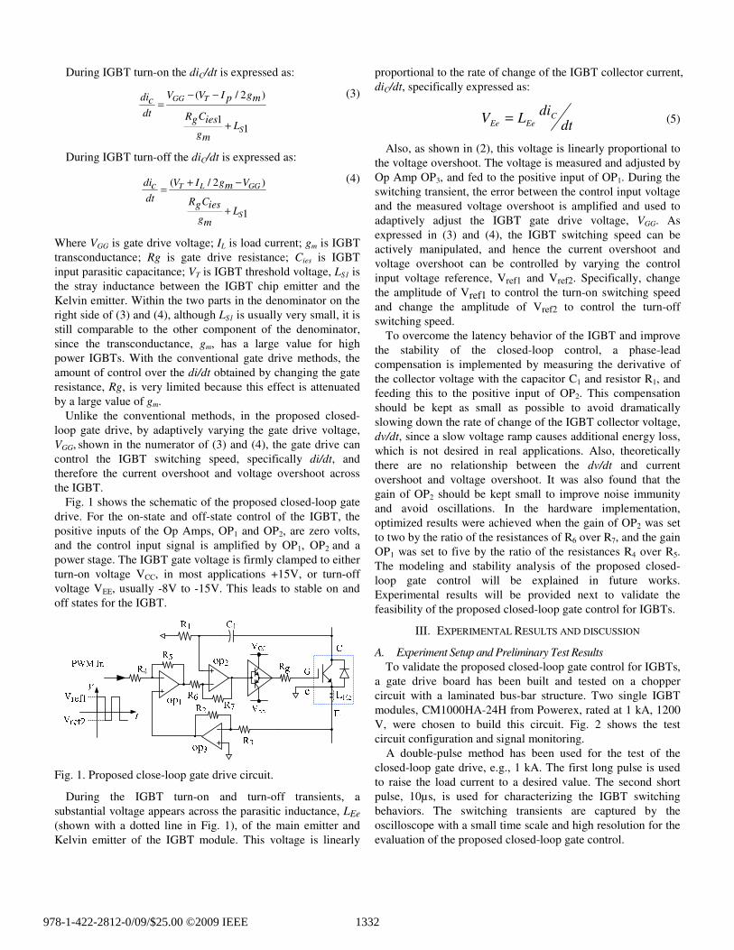
To validate the proposed closed-loop gate control for IGBTs,
a gate drive board has been built and tested on a chopper
circuit with a laminated bus-bar structure. Two single IGBT
modules, CM1000HA-24H from Powerex, rated at 1 kA, 1200
V, were chosen to build this circuit. Fig. 2 shows the test
circuit configuration and signal monitoring.
A double-pulse method has been used for the test of the
closed-loop gate drive, e.g., 1 kA. The first long pulse is used
to raise the load current to a desired value. The second short
pulse, 10µs, is used for characterizing the IGBT switching
behaviors. The switching transients are captured by the
oscilloscope with a small time scale and high resolution for the
evaluation of the proposed closed-loop gate control.
978-1-422-2812-0/09/$25.00 ©2009 IEEE 1332
Fig. 2. Test circuit configuration and signal monitoring.
The preliminary testing was first conducted with a
conventional gate control (CGD) by simply disconnecting the
feed back inputs to the proposed gate drive board. To avoid
damaging the IGBTs, an applied dc bus voltage, Vdc, of 300 V
was used and the load inductor current was initially charged to
1 kA Fig. 3 shows the turn-off waveforms of the gate-emitter
voltage, Vge, collector current Ic, and collector-emitter voltage
Vce. Using the math function of the oscilloscope, the turn-off
energy loss was measured by integrating the product of the Vce
and Ic. A voltage spike as high as 780 V was detected during
the testing. The magnitude of the rate of change of the IGBT
collector current is as high as 3700 A/µs. Fig. 3 also shows that
the energy loss for each turn-off transient is about 0.17 J.
Fig. 3. IGBT turn-off waveforms with CGD (Vdc=300V).
Fig. 4 shows the turn-on transient waveforms. A current
spike as high as 160 A was detected during the testing. The
rate of change of the IGBT collector current, di/dt, is 1600
A/µs, and the measured energy loss, Eon, for this turn-on
transient is about 29 mJ. There are also oscillations which
appear on the Vce waveform before the IGBT turn-on which
are a result of the turn-off of the IGBT. Because there is only
10 µs between the end of the first pulse and the start of the
second pulse, and the CGD turn-off control is employed in the
preliminary test, the oscillation caused by the IGBT turn-off
transient has not yet been fully damped.
Fig. 4. IGBT turn-on waveforms with CGD (Ic=1 kA).
B. Test Results of Closed–Loop Turn-off Control
For comparison, the closed-loop turn-off control tests were
performed, at first with a dc bus voltage of 300 V, which is the
same as that used for the preliminary test. The load inductor
current was also initially charged to 1 kA. Fig. 5 through 7
show the turn-off waveforms using different control voltage
references, Vref2, of -10V, -5V, and -2.5 V, respectively. As
shown in the figures, the voltage overshoot has been
effectively controlled to 310 V, 180V, and 100V; while the rate
of change of the IGBT collector current, di/dt, are 2150 A/µs,
1020 A/µs, and 580 A/µs, respectively. However, Fig. 5
through 7 also show that the initial rate of change of the
collector voltage, dv/dt, is nearly the same in all three tests, and
is comparable to that of CGD result shown in Fig. 3. Therefore,
the energy loss associated with the collector voltage rise ramp
is minimized in the proposed gate drive.
From the test waveforms, the parasitic inductance of the test
circuit can be estimated at about 150 nH. Compared to the
CGD Vge waveform shown in Fig. 3, the gate terminal
voltages shown in Fig. 5 through 7 have been adaptively pulled
up during the turn-off transient while the IGBT collector
current is decreasing. As a result, the gate discharge current
was decreased and the di/dt is limited; and the voltage
overshoot was controlled according to the reference Vref2. It
should be pointed out here that the measured Vge waveform is
the voltage across the IGBT external gate-Kelvin emitter
terminals, and that this is slightly different from the gate
voltage of the internal IGBT chip because of additional voltage
drops on the parasitic components within the gate drive path.
Examining Fig. 5 through 7, it can be shown that when the
switching speed and voltage overshoot are controlled to be
lower, the Vce oscillation amplitude after the first voltage
overshoot hump becomes smaller. Actually there are almost no
oscillations appearing in Fig. 7, because the energy stored in
the parasitic inductances and capacitances has been effectively
discharged during the switching transient (an equivalent circuit
model to study this oscillation phenomenon has been
developed, but omitted here due to page limitation). As a result,
the EMI problems associated with fast switching and
oscillations can also be mitigated when the switching speed is
controlled.
978-1-422-2812-0/09/$25.00 ©2009 IEEE 1333
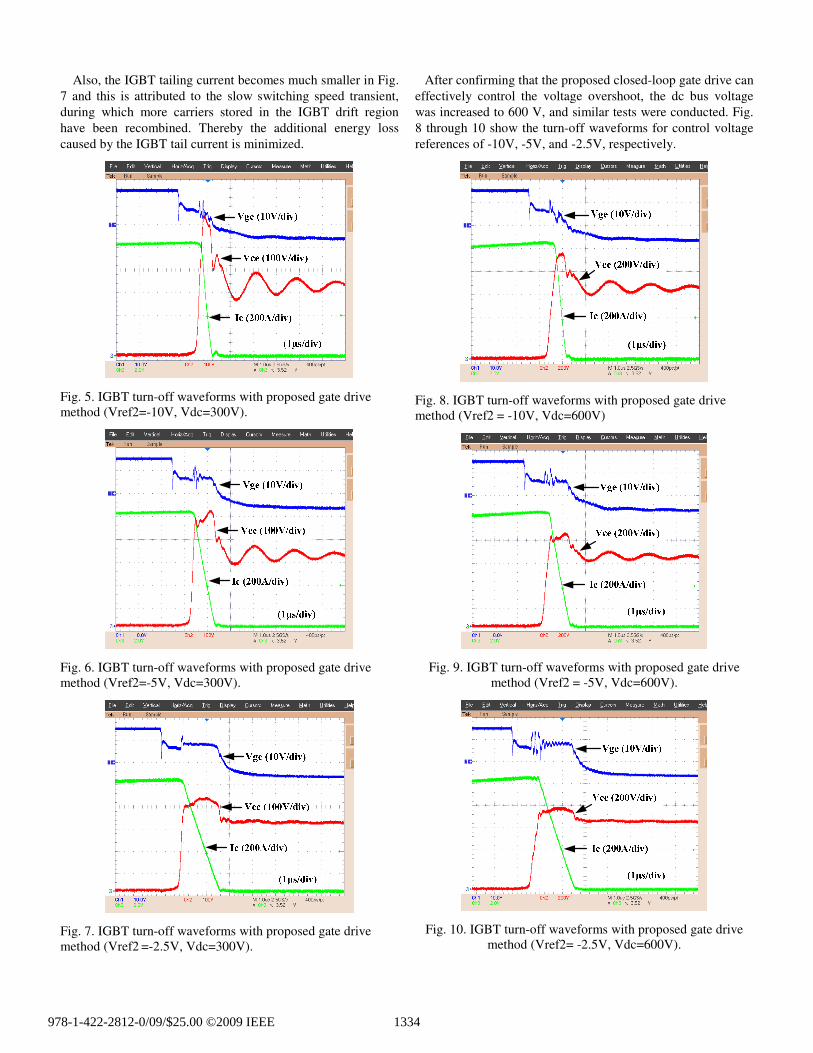
Also, the IGBT tailing current becomes much smaller in Fig.
7 and this is attributed to the slow switching speed transient,
during which more carriers stored in the IGBT drift region
have been recombined. Thereby the additional energy loss
caused by the IGBT tail current is minimized.
Fig. 5. IGBT turn-off waveforms with proposed gate drive
method (Vref2=-10V, Vdc=300V).
Fig. 6. IGBT turn-off waveforms with proposed gate drive
method (Vref2=-5V, Vdc=300V).
Fig. 7. IGBT turn-off waveforms with proposed gate drive
method (Vref2 =-2.5V, Vdc=300V).
After confirming that the proposed closed-loop gate drive can
effectively control the voltage overshoot, the dc bus voltage
was increased to 600 V, and similar tests were conducted. Fig.
8 through 10 show the turn-off waveforms for control voltage
references of -10V, -5V, and -2.5V, respectively.
Fig. 8. IGBT turn-off waveforms with proposed gate drive
method (Vref2 = -10V, Vdc=600V)
Fig. 9. IGBT turn-off waveforms with proposed gate drive
method (Vref2 = -5V, Vdc=600V).
Fig. 10. IGBT turn-off waveforms with proposed gate drive
method (Vref2= -2.5V, Vdc=600V).
978-1-422-2812-0/09/$25.00 ©2009 IEEE 1334
These results shown in Fig. 8 through 10 demonstrated that
the Vos and di/dt was also effectively controlled according to
the reference Vref2, and the numerical values of Vos and di/dt
are same as those shown in Fig 5 through 7, respectively. It can
conclude that the proposed closed-loop gate drive can
effectively control the voltage overshoot and di/dt according to
a control reference independent of dc voltages. Also the Vce
oscillation mitigation phenomena are examined in the test
results shown in Fig 8 through 10.
C. Test Results of Closed-Loop Turn-on Control
During the closed-loop turn-on control tests, the load
inductor current was also initially charged by the first long
pulse to 1 kA, which is the same as that used for the
preliminary test with CGD control. The turn-on transient of the
second short pulse is captured for performance evaluation. Fig.
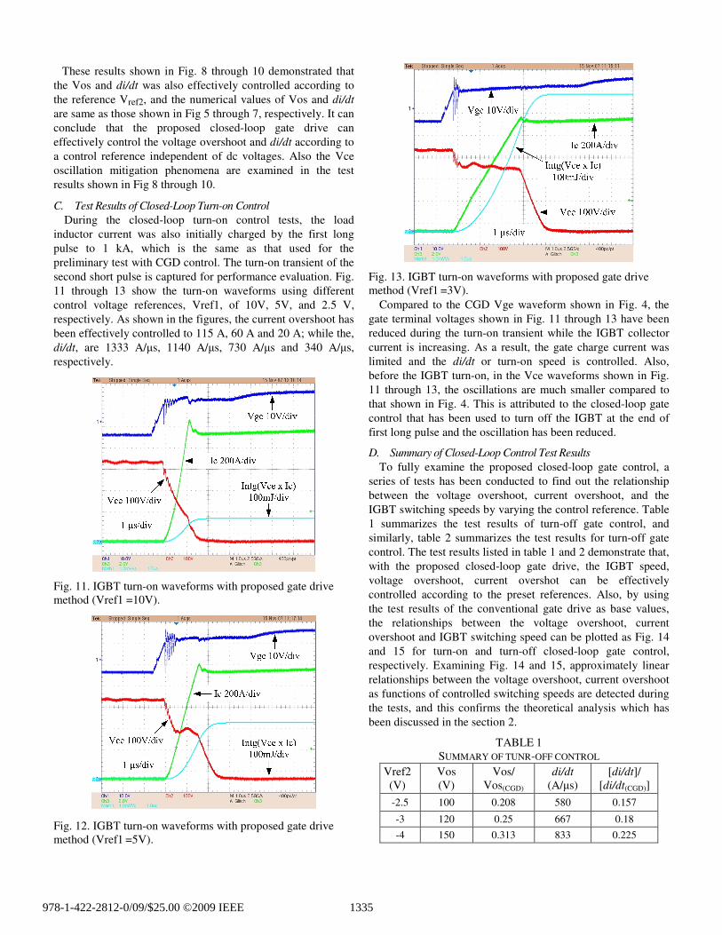
11 through 13 show the turn-on waveforms using different
control voltage references, Vref1, of 10V, 5V, and 2.5 V,
respectively. As shown in the figures, the current overshoot has
been effectively controlled to 115 A, 60 A and 20 A; while the,
di/dt, are 1333 A/µs, 1140 A/µs, 730 A/µs and 340 A/µs,
respectively.
Fig. 11. IGBT turn-on waveforms with proposed gate drive
method (Vref1 =10V).
Fig. 12. IGBT turn-on waveforms with proposed gate drive
method (Vref1 =5V).
Fig. 13. IGBT turn-on waveforms with proposed gate drive
method (Vref1 =3V).
Compared to the CGD Vge waveform shown in Fig. 4, the
gate terminal voltages shown in Fig. 11 through 13 have been
reduced during the turn-on transient while the IGBT collector
current is increasing. As a result, the gate charge current was
limited and the di/dt or turn-on speed is controlled. Also,
before the IGBT turn-on, in the Vce waveforms shown in Fig.
11 through 13, the oscillations are much smaller compared to
that shown in Fig. 4. This is attributed to the closed-loop gate
control that has been used to turn off the IGBT at the end of
first long pulse and the oscillation has been reduced.
D. Summary of Closed-Loop Control Test Results
To fully examine the proposed closed-loop gate control, a
series of tests has been conducted to find out the relationship
between the voltage overshoot, current overshoot, and the
IGBT switching speeds by varying the control reference. Table
1 summarizes the test results of turn-off gate control, and
similarly, table 2 summarizes the test results for turn-off gate
control. The test results listed in table 1 and 2 demonstrate that,
with the proposed closed-loop gate drive, the IGBT speed,
voltage overshoot, current overshot can be effectively
controlled according to the preset references. Also, by using
the test results of the conventional gate drive as base values,
the relationships between the voltage overshoot, current
overshoot and IGBT switching speed can be plotted as Fig. 14
and 15 for turn-on and turn-off closed-loop gate control,
respectively. Examining Fig. 14 and 15, approximately linear
relationships between the voltage overshoot, current overshoot
as functions of controlled switching speeds are detected during
the tests, and this confirms the theoretical analysis which has
been discussed in the section 2.
TABLE 1
SUMMARY OF TUNR-OFF CONTROL
Vref2
(V)
Vos
(V)
Vos/
Vos(CGD)
di/dt
(A/µs)
[di/dt]/
[di/dt(CGD)]
-2.5 100 0.208 580 0.157
-3 120 0.25 667 0.18
-4 150 0.313 833 0.225
978-1-422-2812-0/09/$25.00 ©2009 IEEE 1335
-5 180 0.375 1020 0.276
-6 200 0.417 1140 0.308
-7 220 0.458 1290 0.349
-8 240 0.5 1480 0.4
-9 280 0.583 1800 0.486
-10 310 0.658 2150 0.581
CGD 480 1 3700 1
TABLE 2
SUMMARY OF TURN-ON CONTROL
Vref1
(V)
Irr
(A)
Irr/
Irr(CGD)
di/dt
(A/µs)
[di/dt]/
[di/dt(CGD)]
3 20 0.125 340 0.213
4 45 0.281 590 0.369
5 60 0.375 730 0.456
6 70 0.438 940 0.588
7 95 0.594 1140 0.713
8 110 0.688 1230 0.769
10 115 0.719 1333 0.833
CGD 160 1 1600 1
Fig. 14. Voltage overshoot vs. turn-off switching speed.
Fig. 15. Current overshoot vs. turn-on switching speed.
IV. CONCLUSIONS
A closed-loop gate drive method was proposed to actively
control the switching speed according to a preset control
reference. Compared to the conventional gate drive solutions,
the proposed method has the following advantages:
• The switching speed can be adaptively manipulated
according to preset control references. As a result, the
current overshoot and voltage overshoot can be effectively
controlled and the full capability of the power device can
be used with the proposed gate drive;
• This method enables programmable switching speed
control by dynamically changing the PWM signal
amplitudes. This feature can be illustrated in Fig. 16 and
17. The PWM gate signal duty ratio is used to control the
device’s on-state and off-state time and the PWM gate
signal amplitudes can be used to control the device’s turn-
on and turn-off speeds;
Fig. 16. Control both the duty cycle and switching speed by a
gate PWM signal.
Fig. 17. Conventional (top) and proposed (bottom) PWM gate
control signals.
• The proposed gate drive fully utilizes gate drive signal
information of amplitude and duty cycle (two control
freedoms). As a result, both the power electronic circuit’s
steady-state and transient behaviors can be effectively
978-1-422-2812-0/09/$25.00 ©2009 IEEE 1336
controlled by the system modulator. This new concept has
not been seen from previous works and literatures;
• The proposed gate control enables power device
snubberless operation without additional clamping circuits;
therefore, the power conversion systems design can be
simplified;
• Oscillations are reduced during IGBT switching and the
associated EMI problems can be mitigated;
• Simple circuit and low cost allow easy embedding into the
gate drive circuit.
The investigation also find that, compared with the CGD
methods, the proposed gate control method can actively control
the IGBT turn-off speed under over-current conditions caused
by overload operation or fault short circuit, and limit the
voltage overshoot independent of dc bus voltage and fault
current levels. In addition, the relationships between the
voltage overshoot, current overshoot and associated energy
losses as functions of controlled switching speed has been
derived and can provide guidelines for practical design. The
modeling of the IGBT and a mathematical analysis of the
proposed gate control has been also conducted to confirm the
proposed new method. All these results will be presented in
future works.
REFERENCES
[1] H. R. Muhammad, “Power Electronics-Circuits, Devices,
and Applications,” 3rd
edition, Upper Saddle River, NJ,
Pearson Prentice Hall, 2004.
[2] A. R. Hefner, Jr., “An Investigation of the Drive Circuit
Requirements for the Power Insulated Gate Bipolar
Transistor (IGBT),” IEEE Trans. on Power Electronics,
vol. 6, issue 2, April 1991 pp. 208 – 219.
[3] F. Blaabjerg and J. K. Pederson, “An optimum drive and
clamp circuit design with controlled switching for a
snubberless PWM-VSI-IGBT inverter leg,” in Proc. IEEE
PESC’92, 1992, pp. 289–297.
[4] R. Chokhawala, J. Catt, and B. Pelly, “Gate drive
considerations for IGBT Modules,” in Conf. Rec. IEEE-
IAS Annu. Meeting, 1992, pp. 1186–1195.
[5] H. G. Eckel and L. Sack, “Optimization of the turn-off
performance of IGBT at over-current and short-circuit
current,” in Proc. EPE’93, 1993, pp. 317–322.
[6] H. Lee, Y. Lee, B. Suh, and D. Hyun, “An Improved Gate
Control Scheme for Snubberless Operation of High Power
IGBTs,” IEEE-IAS 1997, pp. 975-982.
[7] J. P. Berry, “MOSFET operating under hard switching
mode: voltage and current gradients control,” EPE conf.
1991, pp. 130-134, Italy, 1991.
[8] A. N. Githiari, R. J. Leedham, and P. R. Palmer, “High
performance gate drives utilizing the IGBT in the active
region,” in Proc. IEEE PESC’96, 1996, pp. 1754–1759.
[9] S. Igarashi, S. Takizawa, M. Tabata, M. Takei, and K.
Kuroki, “An Active Gate Drive Circuit for IGBTs to
Realize Low-noise and Snubberless System,” ISPSD,
1997, pp. 69-72.
[10] S. Musumeci, A. Raciti, A. Testa, A. Galluzzo, and M.
Melito, “A new adaptive driving technique for high
current gate controlled devices,” in Proc. IEEE APEC,
1994, pp. 480–486.
[11] V. John, B. Suh and T.A. Lipo, "High performance active
gate drive for high power IGBTs," IEEE Trans. Industry
Appl., VOL. 35, NO. 5, Sept./Oct. 1999.pp.1108-1117.
[12] L. Dulau, S. Pontarollo, A. Boimond, J. Garnier, N.
Giraudo, and O. Terrasse, “A new gate driver integrated
circuit for IGBT Devices With Advanced Protections,”
IEEE Trans. Power Electronics, VOL. 21, NO. 1,
JANUARY 2006, pp. 38-44.
[13] C. Gerster and P. Hofer, “Gate-controlled dv/dt and di/dt
limitation in high power IGBT converters,” EPE Journal,
Vol. 5, no 3/4, January 1996, page 11-16.
[14] H. R. uedi and P. K. ohli, “Dynamic Gate Controller
(DGC) – A new IGBT Gate Unit for High Current/ High
Voltage IGBT Modules,” PCIM 1995, pp. 241-249.
[15] T. Reimann, R. Krummer, and J. Petzoldt, “Active
Voltage Clamping Techniques for Over-voltage Protection
of MOS-Controlled Power Transistors,” EPE 1997, pp.
4043-4048.
[16] C. Gerster and P. Hofer, “Gate-controlled dv/dt and di/dt
limitation in high power IGBT converters,” EPE Journal,
Vol. 5, no 3/4, January 1996, page 11-16.
[17] P. R. Palmer and A. N. Githiari, “The Series Connection
of IGBTs with Active Voltage Sharing,” IEEE Trans. on
Power Electronics, vol. 12, No.4, pp. 637-644, 1997.
[18] P. R. Palmer, A. N. Githiari, and R. J. Leedham, “Some
scaling issues in the active control of IGBT modules for
high power applications,” in IEEE PESC 1997, pp. 854–
860.
[19] P. R. Palmer, P. Y. Eng, J. C. Joyce, J. Hudgins, E. Santi,
and R. Dougal, “Circuit simulator models for the diode
and IGBT with full temperature dependent features,” in
IEEE PESC 2001, pp. 2171–2177.
[20] P. R. Palmer and H. S. Rajamani, “Active voltage control
of IGBTs for high power applications,” IEEE Trans.
Power Electron., vol. 19, no. 4, pp. 894–901, Jul. 2004.
[21] Y. Wang, A. T. Bryant, P. R. Palmer, S. J. Finney, M.
Abu-Khaizaran, G. Li, “An analysis of high power IGBT
switching under cascade active voltage control,” IEEE
IAS Annual Meeting , Volume 2, 2-6 Oct. 2005.
[22] Y. Wang, P. R. Palmer T. C. Lim, S. J. Finney, A. T.
Bryant, “Real-time Optimization of IGBT/Diode Cell
Switching under Active Voltage Control,”, IEEE IAS
conference, 8-12 Oct. 2006.
[23] A. T. Bryant,Y. Wang, S. J. Finney, T. C. Lim, and P. R.
Palmer, “Numerical Optimization of an Active Voltage
Controller for High-Power IGBT Converters,” IEEE Tran.
On Power Electronics. VOL. 22, NO. 2, MARCH 2007.
[24] A. T. Bryant, P. R. Palmer, E. Santi, and J. L. Hudgins
“Simulation and Optimization of Diode and Insulated Gate
Bipolar Transistor Interaction in a Chopper Cell Using
MATLAB and Simulink,”, IEEE Tran. On Power
Electronics, VOL. 43, NO. 4, JULY/AUG. 2007.
[25] V. K. Khanna, “IGBT Theory and Design,” IEEE Press,
Wiley-Interscience, 2003.
978-1-422-2812-0/09/$25.00 ©2009 IEEE 1337