coe 405 sequential circuit design review dr. aiman h. el-maleh computer engineering department king...
TRANSCRIPT
COE 405COE 405Sequential Circuit Design Sequential Circuit Design
ReviewReview
COE 405COE 405Sequential Circuit Design Sequential Circuit Design
ReviewReview
Dr. Aiman H. El-Maleh
Computer Engineering Department
King Fahd University of Petroleum & Minerals
Dr. Aiman H. El-Maleh
Computer Engineering Department
King Fahd University of Petroleum & Minerals
1-2
OutlineOutlineOutlineOutline
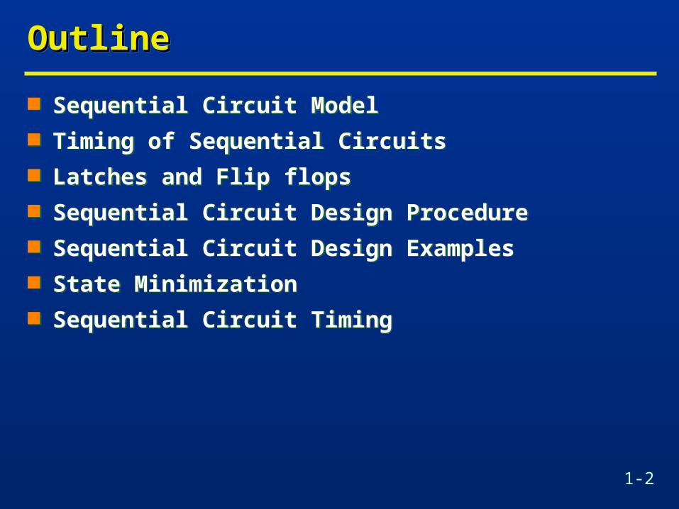
Sequential Circuit Model Timing of Sequential Circuits Latches and Flip flops Sequential Circuit Design Procedure Sequential Circuit Design Examples State Minimization Sequential Circuit Timing
Sequential Circuit Model Timing of Sequential Circuits Latches and Flip flops Sequential Circuit Design Procedure Sequential Circuit Design Examples State Minimization Sequential Circuit Timing
1-3
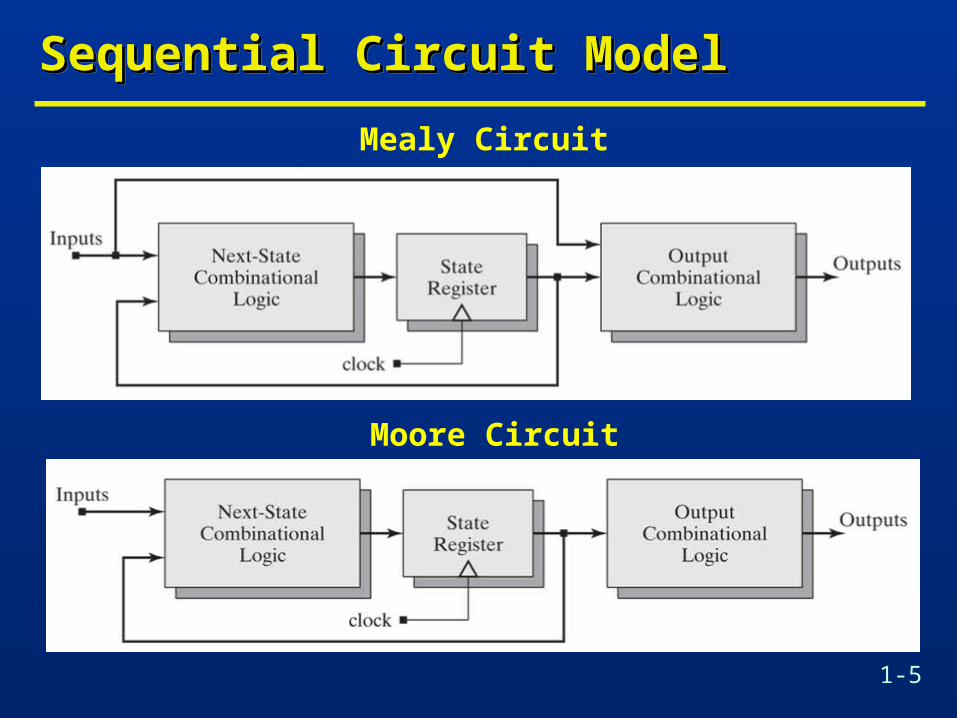
Sequential Circuit ModelSequential Circuit ModelSequential Circuit ModelSequential Circuit Model
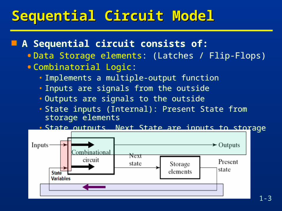
A Sequential circuit consists of:• Data Storage elements: (Latches / Flip-Flops)
• Combinatorial Logic:• Implements a multiple-output function• Inputs are signals from the outside• Outputs are signals to the outside• State inputs (Internal): Present State from storage elements• State outputs, Next State are inputs to storage elements
1-4
Sequential Circuit ModelSequential Circuit ModelSequential Circuit ModelSequential Circuit Model
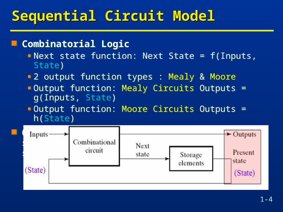
Combinatorial Logic• Next state function: Next State = f(Inputs, State)
• 2 output function types : Mealy & Moore
• Output function: Mealy Circuits Outputs = g(Inputs, State)
• Output function: Moore Circuits Outputs = h(State)
Output function type depends on specification and affects the design significantly
1-5
Sequential Circuit ModelSequential Circuit ModelSequential Circuit ModelSequential Circuit Model
Mealy Circuit
Moore Circuit
1-6
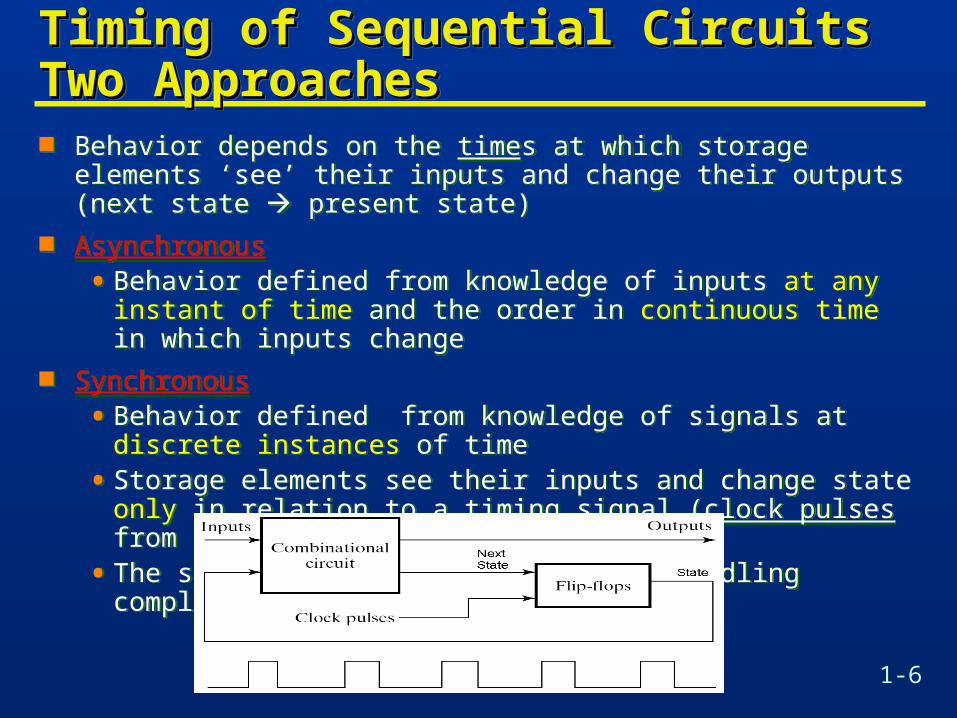
Timing of Sequential CircuitsTiming of Sequential CircuitsTwo ApproachesTwo ApproachesTiming of Sequential CircuitsTiming of Sequential CircuitsTwo ApproachesTwo Approaches Behavior depends on the times at which storage elements ‘see’ their
inputs and change their outputs (next state present state) Asynchronous
• Behavior defined from knowledge of inputs at any instant of time and the order in continuous time in which inputs change
Synchronous
• Behavior defined from knowledge of signals at discrete instances of time
• Storage elements see their inputs and change state only in relation to a timing signal (clock pulses from a clock)
• The synchronous abstraction allows handling complex designs!
Behavior depends on the times at which storage elements ‘see’ their inputs and change their outputs (next state present state)
Asynchronous
• Behavior defined from knowledge of inputs at any instant of time and the order in continuous time in which inputs change
Synchronous
• Behavior defined from knowledge of signals at discrete instances of time
• Storage elements see their inputs and change state only in relation to a timing signal (clock pulses from a clock)
• The synchronous abstraction allows handling complex designs!
1-7
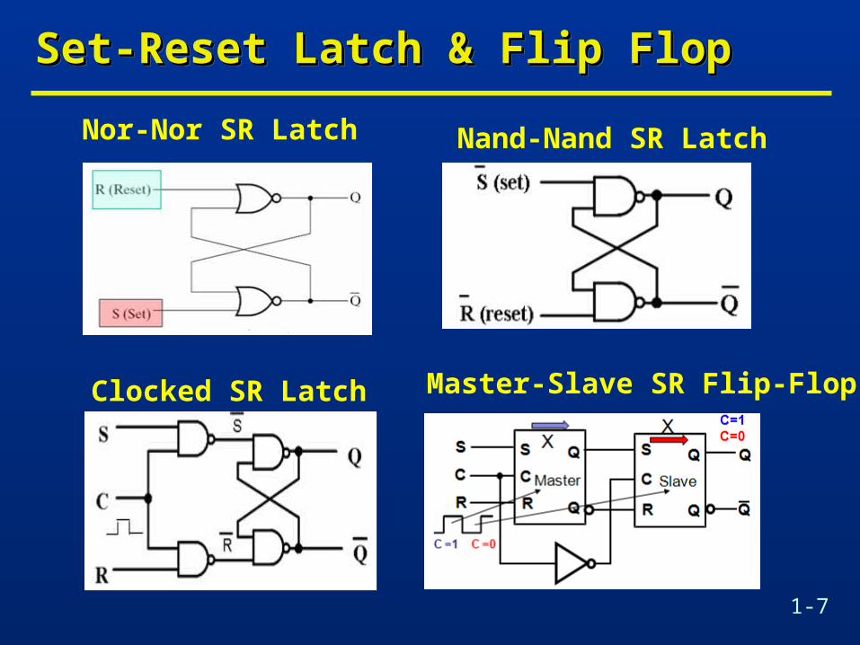
Set-Reset Latch & Flip FlopSet-Reset Latch & Flip FlopSet-Reset Latch & Flip FlopSet-Reset Latch & Flip Flop
Nor-Nor SR Latch Nand-Nand SR Latch
Clocked SR Latch Master-Slave SR Flip-Flop
1-8
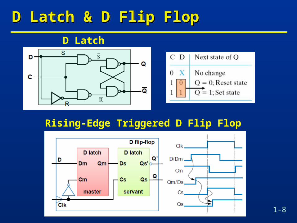
D Latch & D Flip FlopD Latch & D Flip FlopD Latch & D Flip FlopD Latch & D Flip Flop
D Latch
Rising-Edge Triggered D Flip Flop
1-9
Sequential Circuit Design ProcedureSequential Circuit Design ProcedureSequential Circuit Design ProcedureSequential Circuit Design Procedure
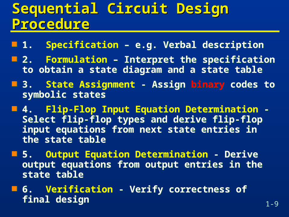
1. Specification – e.g. Verbal description 2. Formulation – Interpret the specification to obtain
a state diagram and a state table 3. State Assignment - Assign binary codes to
symbolic states 4. Flip-Flop Input Equation Determination - Select
flip-flop types and derive flip-flop input equations from next state entries in the state table
5. Output Equation Determination - Derive output equations from output entries in the state table
6. Verification - Verify correctness of final design
1-10
State InitializationState InitializationState InitializationState Initialization
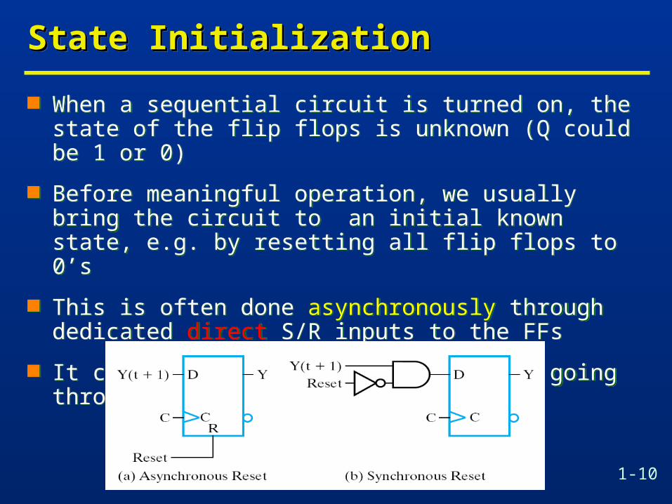
When a sequential circuit is turned on, the state of the flip flops is unknown (Q could be 1 or 0)
Before meaningful operation, we usually bring the circuit to an initial known state, e.g. by resetting all flip flops to 0’s
This is often done asynchronously through dedicated direct S/R inputs to the FFs
It can also be done synchronously by going through the clocked FF inputs
1-11
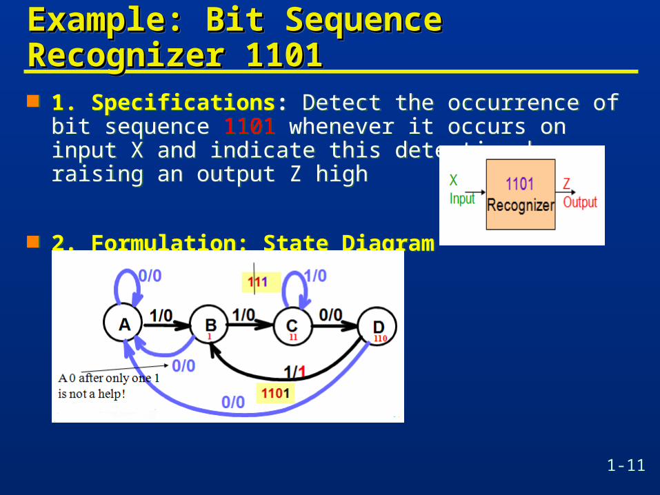
Example: Bit Sequence Recognizer Example: Bit Sequence Recognizer 11011101Example: Bit Sequence Recognizer Example: Bit Sequence Recognizer 11011101 1. Specifications: Detect the occurrence of bit sequence
1101 whenever it occurs on input X and indicate this detection by raising an output Z high
2. Formulation: State Diagram
1. Specifications: Detect the occurrence of bit sequence 1101 whenever it occurs on input X and indicate this detection by raising an output Z high
2. Formulation: State Diagram
1-12
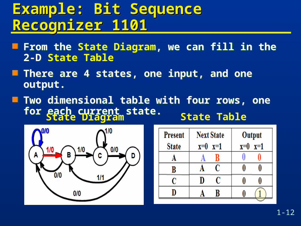
Example: Bit Sequence Recognizer Example: Bit Sequence Recognizer 11011101Example: Bit Sequence Recognizer Example: Bit Sequence Recognizer 11011101 From the State Diagram, we can fill in the 2-D State
Table There are 4 states, one input, and one output. Two dimensional table with four rows, one for each
current state.
From the State Diagram, we can fill in the 2-D State Table
There are 4 states, one input, and one output. Two dimensional table with four rows, one for each
current state.
State Diagram State Table
1-13
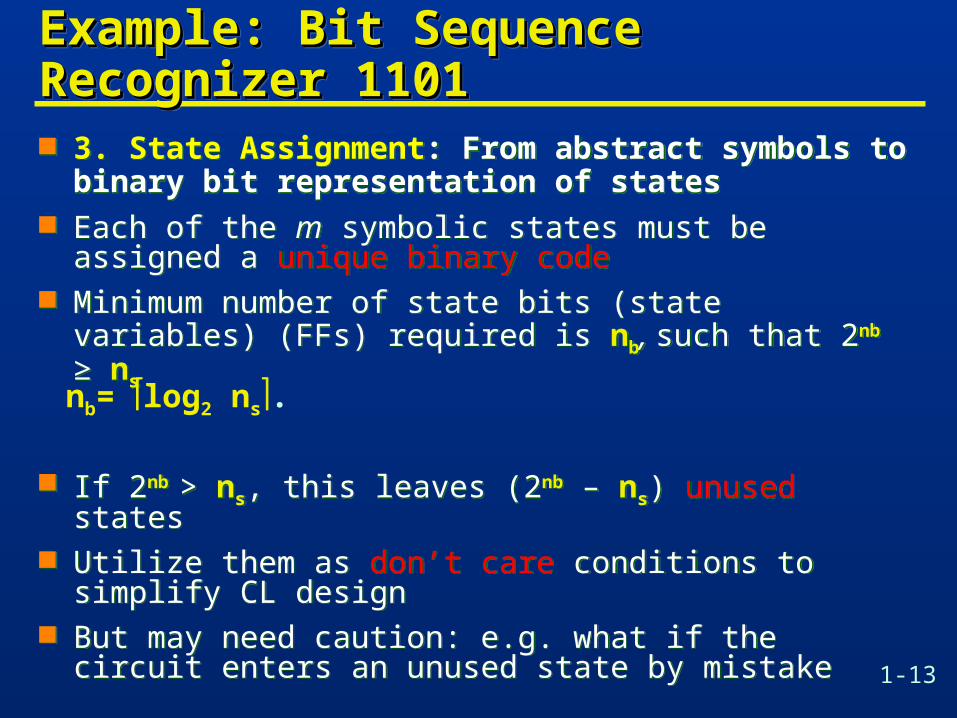
Example: Bit Sequence Recognizer Example: Bit Sequence Recognizer 11011101Example: Bit Sequence Recognizer Example: Bit Sequence Recognizer 11011101 3. State Assignment: From abstract symbols to binary
bit representation of states Each of the m symbolic states must be assigned a unique
binary code Minimum number of state bits (state variables) (FFs)
required is nb, such that 2nb ≥ ns
If 2nb > ns, this leaves (2nb – ns) unused states Utilize them as don’t care conditions to simplify CL design But may need caution: e.g. what if the circuit enters an
unused state by mistake
3. State Assignment: From abstract symbols to binary bit representation of states
Each of the m symbolic states must be assigned a unique binary code
Minimum number of state bits (state variables) (FFs) required is nb, such that 2nb ≥ ns
If 2nb > ns, this leaves (2nb – ns) unused states Utilize them as don’t care conditions to simplify CL design But may need caution: e.g. what if the circuit enters an
unused state by mistake
nb= log2 ns.
1-14
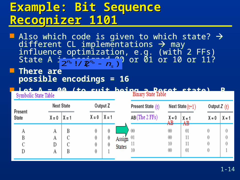
Example: Bit Sequence Recognizer Example: Bit Sequence Recognizer 11011101Example: Bit Sequence Recognizer Example: Bit Sequence Recognizer 11011101 Also which code is given to which state? different CL
implementations may influence optimization, e.g. (with 2 FFs) State A is assigned 00 or 01 or 10 or 11?
There are possible encodings = 16 Let A = 00 (to suit being a Reset state), B = 01, C = 11,
D = 10
Also which code is given to which state? different CL implementations may influence optimization, e.g. (with 2 FFs) State A is assigned 00 or 01 or 10 or 11?
There are possible encodings = 16 Let A = 00 (to suit being a Reset state), B = 01, C = 11,
D = 10
)!2/(!2 snn nbb
1-15
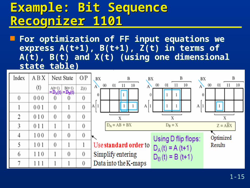
Example: Bit Sequence Recognizer Example: Bit Sequence Recognizer 11011101Example: Bit Sequence Recognizer Example: Bit Sequence Recognizer 11011101 For optimization of FF input equations we express
A(t+1), B(t+1), Z(t) in terms of A(t), B(t) and X(t) (using one dimensional state table)
For optimization of FF input equations we express A(t+1), B(t+1), Z(t) in terms of A(t), B(t) and X(t) (using one dimensional state table)
1-16
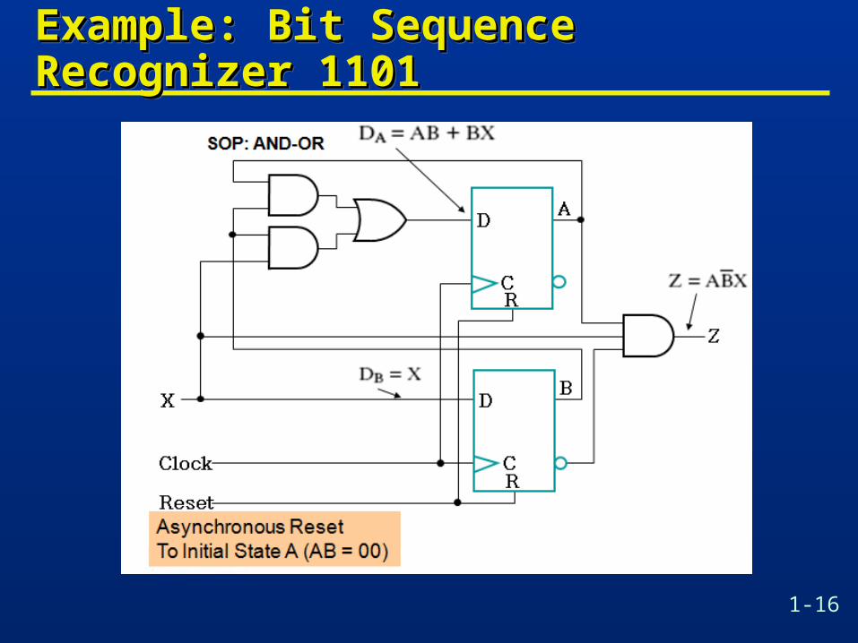
Example: Bit Sequence Recognizer Example: Bit Sequence Recognizer 11011101Example: Bit Sequence Recognizer Example: Bit Sequence Recognizer 11011101
1-17
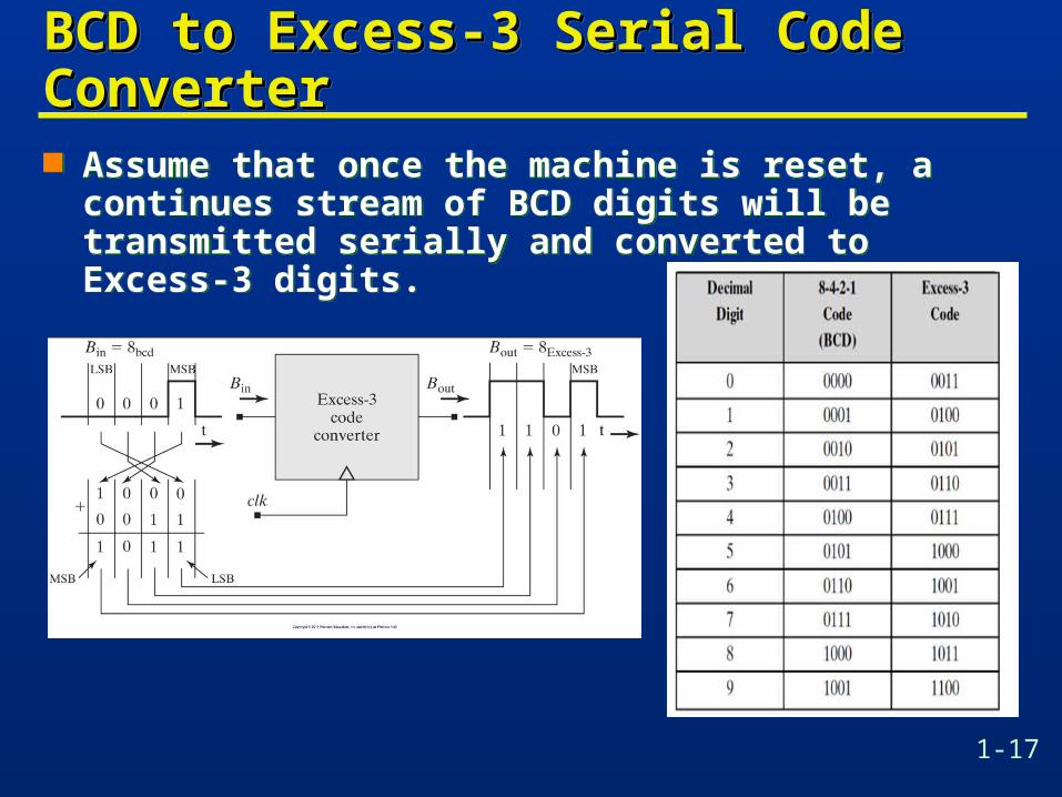
BCD to Excess-3 Serial Code BCD to Excess-3 Serial Code ConverterConverterBCD to Excess-3 Serial Code BCD to Excess-3 Serial Code ConverterConverter Assume that once the machine is reset, a continues
stream of BCD digits will be transmitted serially and converted to Excess-3 digits.
Assume that once the machine is reset, a continues stream of BCD digits will be transmitted serially and converted to Excess-3 digits.
1-18
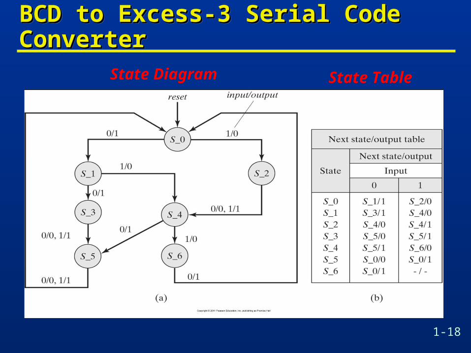
BCD to Excess-3 Serial Code BCD to Excess-3 Serial Code ConverterConverterBCD to Excess-3 Serial Code BCD to Excess-3 Serial Code ConverterConverter
State Diagram State Table
1-19
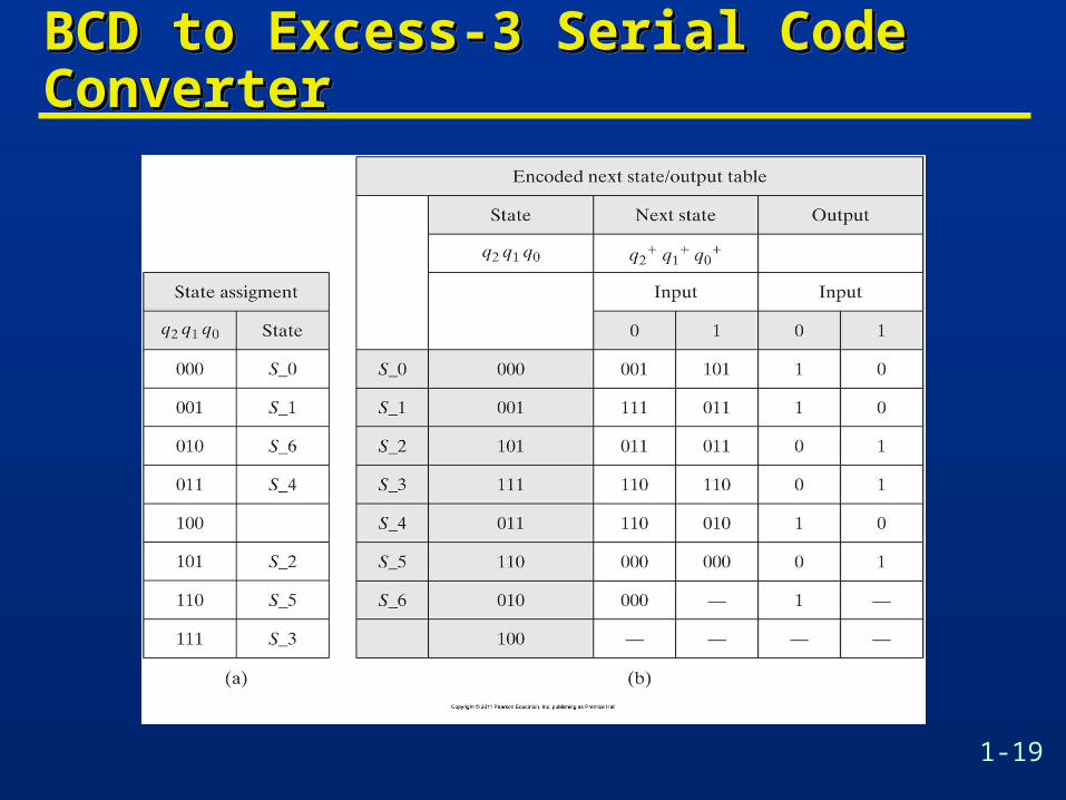
BCD to Excess-3 Serial Code BCD to Excess-3 Serial Code ConverterConverterBCD to Excess-3 Serial Code BCD to Excess-3 Serial Code ConverterConverter
1-20
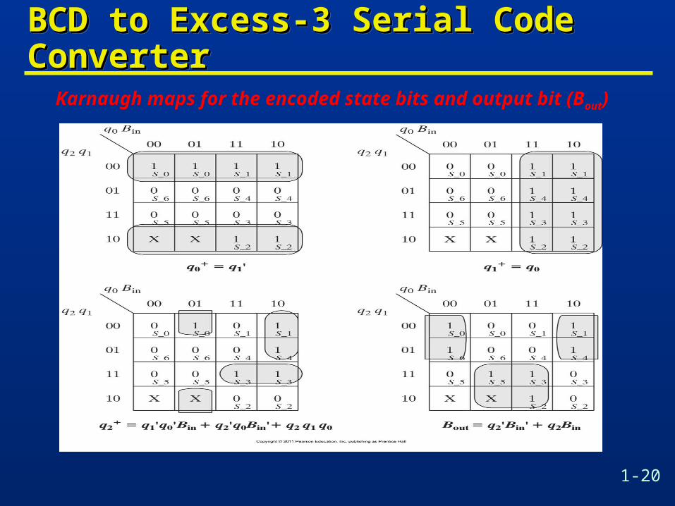
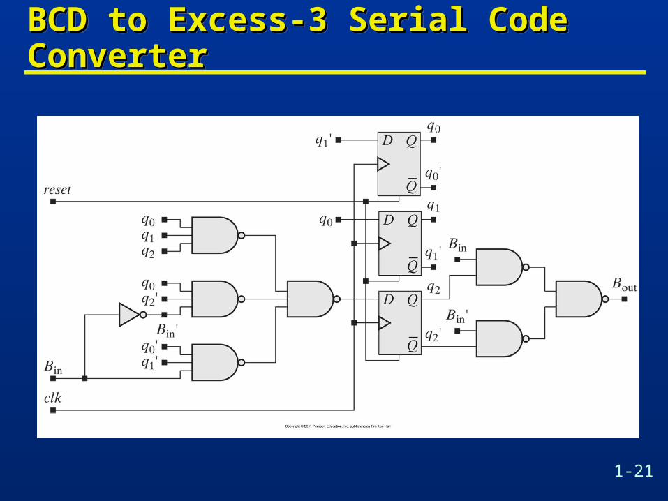
BCD to Excess-3 Serial Code BCD to Excess-3 Serial Code ConverterConverterBCD to Excess-3 Serial Code BCD to Excess-3 Serial Code ConverterConverter
Karnaugh maps for the encoded state bits and output bit (Bout)
1-21
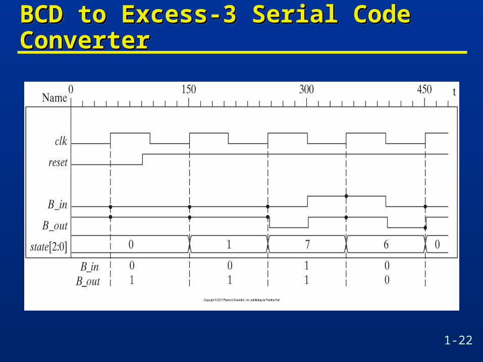
BCD to Excess-3 Serial Code BCD to Excess-3 Serial Code ConverterConverterBCD to Excess-3 Serial Code BCD to Excess-3 Serial Code ConverterConverter
1-22
BCD to Excess-3 Serial Code BCD to Excess-3 Serial Code ConverterConverterBCD to Excess-3 Serial Code BCD to Excess-3 Serial Code ConverterConverter
1-23
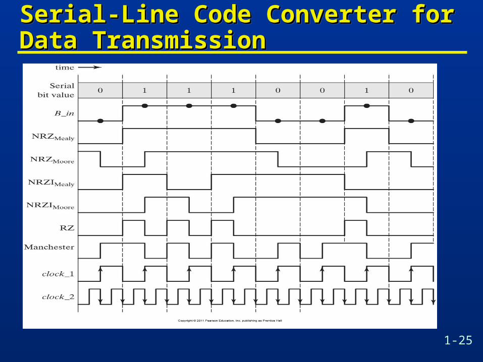
Serial-Line Code Converter for Data Serial-Line Code Converter for Data TransmissionTransmissionSerial-Line Code Converter for Data Serial-Line Code Converter for Data TransmissionTransmission Line codes are used in data transmission or storage
systems to reduce effects of noise in serial communication channels.
Receiver of data must be able to operate synchronosly with sending unit.
Code converters transform data stream into a format encoded to enable receiver to recover data.
A phase lock loop (PLL) can recover clock from line data• If no long series of 1’s or 0’s in data encoded in non-return-to-
zero (NRZ) format
• If no long series of 0’s in data encoded in non-return-to-zero invert-on-ones (NRZI) format or return-to-zero (RZ) format
• Always for Manchester format.
Line codes are used in data transmission or storage systems to reduce effects of noise in serial communication channels.
Receiver of data must be able to operate synchronosly with sending unit.
Code converters transform data stream into a format encoded to enable receiver to recover data.
A phase lock loop (PLL) can recover clock from line data• If no long series of 1’s or 0’s in data encoded in non-return-to-
zero (NRZ) format
• If no long series of 0’s in data encoded in non-return-to-zero invert-on-ones (NRZI) format or return-to-zero (RZ) format
• Always for Manchester format.
1-24
Serial-Line Code Converter for Data Serial-Line Code Converter for Data TransmissionTransmissionSerial-Line Code Converter for Data Serial-Line Code Converter for Data TransmissionTransmission NRZ Code: duplicates the bit pattern of the input signal NRZI Code: the output remains constant as long as the
input is 0 and toggles if the input is 1. RZ Code: a 0 is transmitted as a 0, while a 1 is
transmitted as a 1 for the first half of the bit time and a 0 for the remaining bit time.
Manchester Code: a 0 is transmitted as a 0 for the first half of the bit time and a 1 for the remaining bit time, while a 1 is transmitted as a 1 for the first half of the bit time and a 0 for the remaining bit time.
NRZ Code: duplicates the bit pattern of the input signal NRZI Code: the output remains constant as long as the
input is 0 and toggles if the input is 1. RZ Code: a 0 is transmitted as a 0, while a 1 is
transmitted as a 1 for the first half of the bit time and a 0 for the remaining bit time.
Manchester Code: a 0 is transmitted as a 0 for the first half of the bit time and a 1 for the remaining bit time, while a 1 is transmitted as a 1 for the first half of the bit time and a 0 for the remaining bit time.
1-25
Serial-Line Code Converter for Data Serial-Line Code Converter for Data TransmissionTransmissionSerial-Line Code Converter for Data Serial-Line Code Converter for Data TransmissionTransmission
1-26
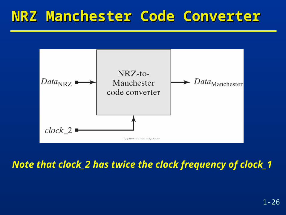
NRZ Manchester Code ConverterNRZ Manchester Code ConverterNRZ Manchester Code ConverterNRZ Manchester Code Converter
Note that clock_2 has twice the clock frequency of clock_1
1-27
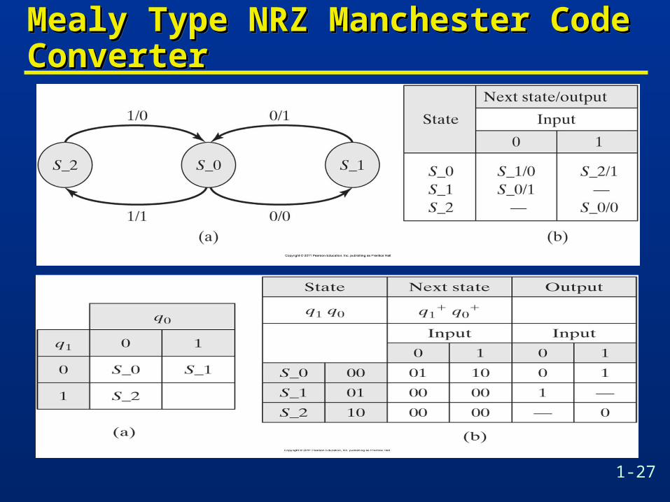
Mealy Type NRZ Manchester Code Mealy Type NRZ Manchester Code ConverterConverterMealy Type NRZ Manchester Code Mealy Type NRZ Manchester Code ConverterConverter
1-28
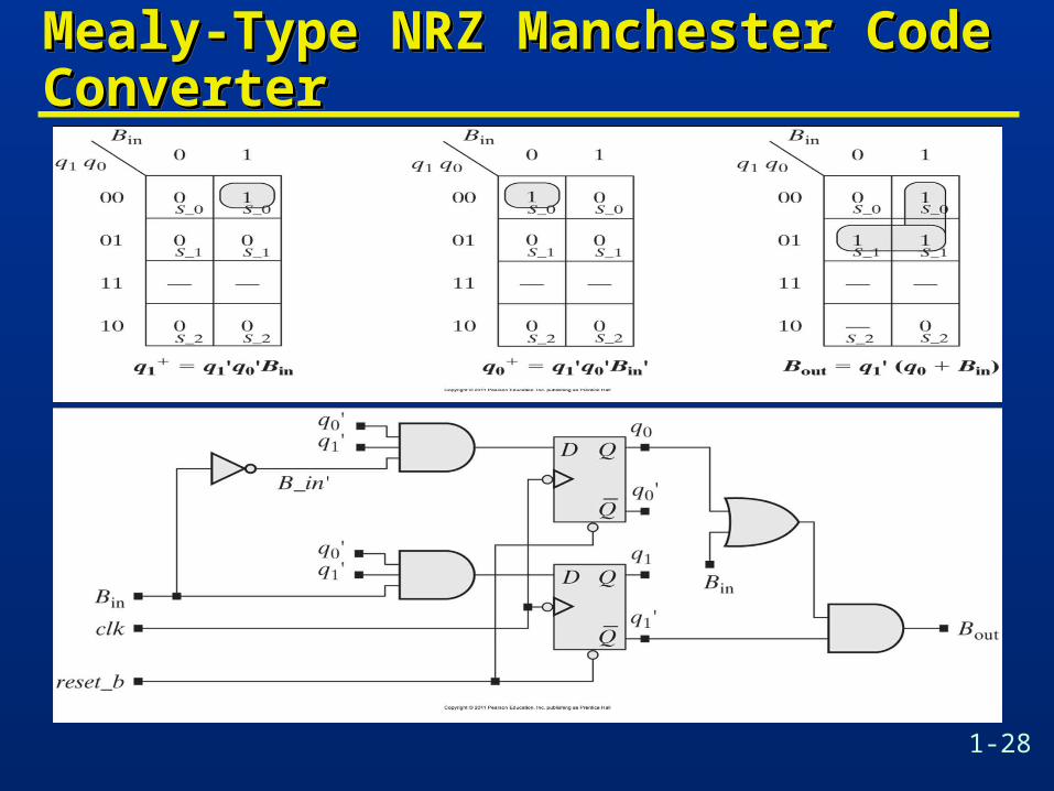
Mealy-Type NRZ Manchester Code Mealy-Type NRZ Manchester Code ConverterConverterMealy-Type NRZ Manchester Code Mealy-Type NRZ Manchester Code ConverterConverter
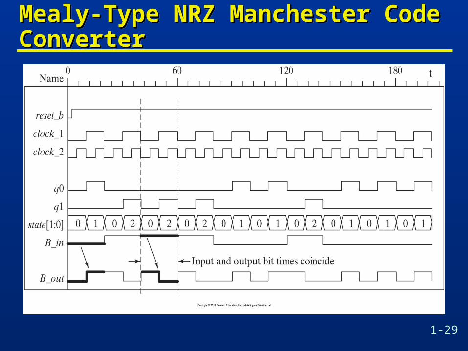
1-29
Mealy-Type NRZ Manchester Code Mealy-Type NRZ Manchester Code ConverterConverterMealy-Type NRZ Manchester Code Mealy-Type NRZ Manchester Code ConverterConverter
1-30
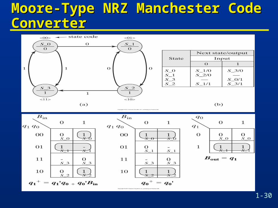
Moore-Type NRZ Manchester Code Moore-Type NRZ Manchester Code ConverterConverterMoore-Type NRZ Manchester Code Moore-Type NRZ Manchester Code ConverterConverter
1-31
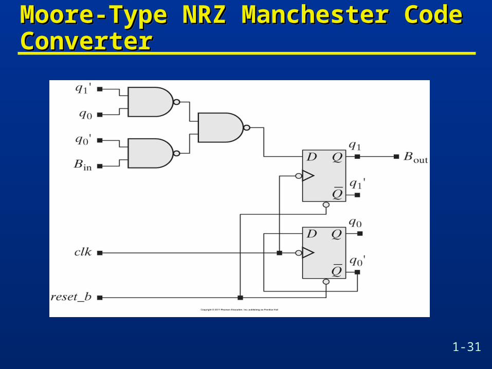
Moore-Type NRZ Manchester Code Moore-Type NRZ Manchester Code ConverterConverterMoore-Type NRZ Manchester Code Moore-Type NRZ Manchester Code ConverterConverter
1-32
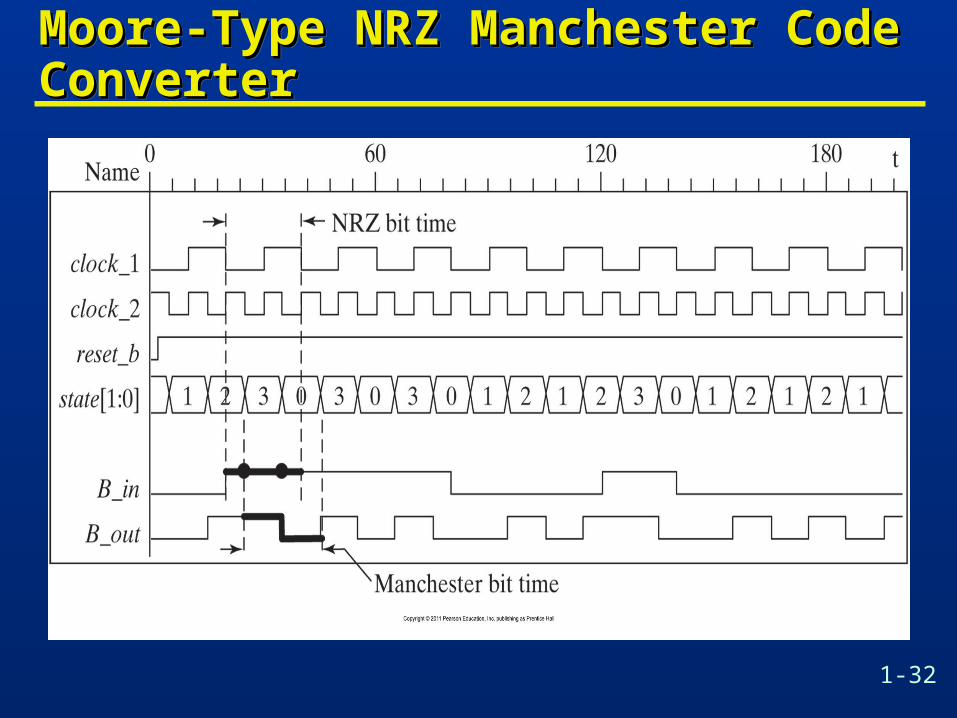
Moore-Type NRZ Manchester Code Moore-Type NRZ Manchester Code ConverterConverterMoore-Type NRZ Manchester Code Moore-Type NRZ Manchester Code ConverterConverter
1-33
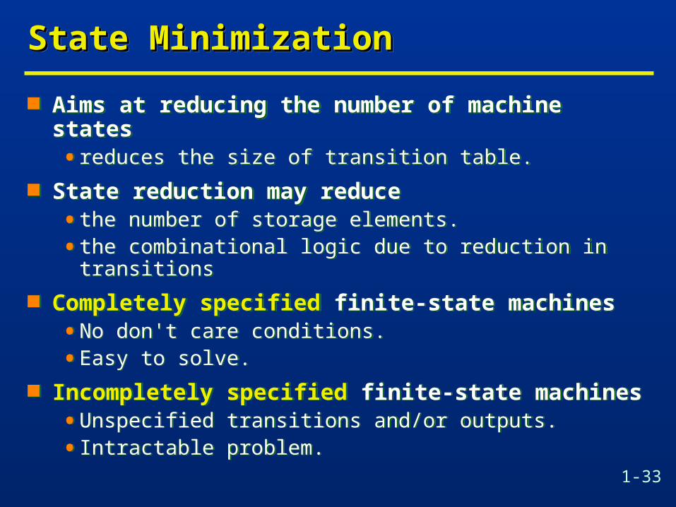
State MinimizationState MinimizationState MinimizationState Minimization
Aims at reducing the number of machine states • reduces the size of transition table.
State reduction may reduce • the number of storage elements.
• the combinational logic due to reduction in transitions
Completely specified finite-state machines• No don't care conditions.
• Easy to solve.
Incompletely specified finite-state machines• Unspecified transitions and/or outputs.
• Intractable problem.
1-34
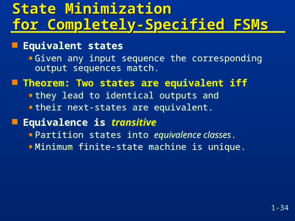
State Minimization State Minimization for Completely-Specified FSMsfor Completely-Specified FSMsState Minimization State Minimization for Completely-Specified FSMsfor Completely-Specified FSMs Equivalent states
• Given any input sequence the corresponding output sequences match.
Theorem: Two states are equivalent iff• they lead to identical outputs and
• their next-states are equivalent.
Equivalence is transitive• Partition states into equivalence classes.
• Minimum finite-state machine is unique.
Equivalent states• Given any input sequence the corresponding output
sequences match.
Theorem: Two states are equivalent iff• they lead to identical outputs and
• their next-states are equivalent.
Equivalence is transitive• Partition states into equivalence classes.
• Minimum finite-state machine is unique.
1-35
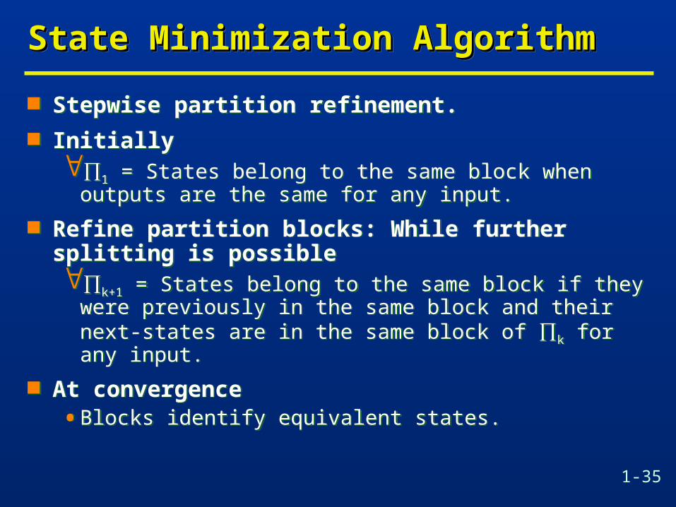
State Minimization AlgorithmState Minimization AlgorithmState Minimization AlgorithmState Minimization Algorithm
Stepwise partition refinement. Initially
1 = States belong to the same block when outputs are the same for any input.
Refine partition blocks: While further splitting is possiblek+1 = States belong to the same block if they were
previously in the same block and their next-states are in the same block of k for any input.
At convergence• Blocks identify equivalent states.
1-36
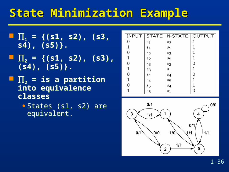
State Minimization ExampleState Minimization ExampleState Minimization ExampleState Minimization Example
1 = {(s1, s2), (s3, s4), (s5)}.
2 = {(s1, s2), (s3), (s4), (s5)}.
2 = is a partition into equivalence classes• States (s1, s2) are equivalent.
1 = {(s1, s2), (s3, s4), (s5)}.
2 = {(s1, s2), (s3), (s4), (s5)}.
2 = is a partition into equivalence classes• States (s1, s2) are equivalent.

1-37
State Minimization ExampleState Minimization ExampleState Minimization ExampleState Minimization Example
Original FSM Minimal FSM

1-38
State Minimization ExampleState Minimization ExampleState Minimization ExampleState Minimization Example
{OUT_0} = IN_0 LatchOut_v1' + IN_0 LatchOut_v3' + IN_0' LatchOut_v2'v4.0 = IN_0 LatchOut_v1' + LatchOut_v1' LatchOut_v2'v4.1 = IN_0' LatchOut_v2 LatchOut_v3 + IN_0' LatchOut_v2'v4.2 = IN_0 LatchOut_v1' + IN_0' LatchOut_v1 + IN_0' LatchOut_v2 LatchOut_v3sis> print_stats pi= 1 po= 1 nodes= 4 latches= 3lits(sop)= 22 #states(STG)= 5
{OUT_0} = IN_0 LatchOut_v1' + IN_0 LatchOut_v2 + IN_0' LatchOut_v2'v3.0 = IN_0 LatchOut_v1' + LatchOut_v1' LatchOut_v2‘v3.1 = IN_0' LatchOut_v1' + IN_0' LatchOut_v2'sis> print_statspi= 1 po= 1 nodes= 3 latches= 2lits(sop)= 14 #states(STG)= 4
Original FSM
Minimal FSM
1-39
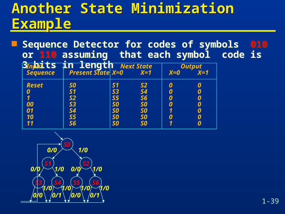
Another State Minimization ExampleAnother State Minimization ExampleAnother State Minimization ExampleAnother State Minimization Example
Sequence Detector for codes of symbols 010 or 110 assuming that each symbol code is 3 bits in length
Sequence Detector for codes of symbols 010 or 110 assuming that each symbol code is 3 bits in length
Input Next State OutputSequence Present State X=0 X=1 X=0 X=1
Reset S0 S1 S2 0 00 S1 S3 S4 0 01 S2 S5 S6 0 000 S3 S0 S0 0 001 S4 S0 S0 1 010 S5 S0 S0 0 011 S6 S0 S0 1 0
S0
S3
S2S1
S5 S6S4
1/00/0
1/0
1/00/1
0/01/00/0
1/00/0
1/00/1
1/00/0
1-40
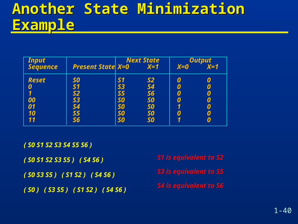
Another State Minimization ExampleAnother State Minimization ExampleAnother State Minimization ExampleAnother State Minimization Example
Input Next State OutputSequence Present State X=0 X=1 X=0 X=1
Reset S0 S1 S2 0 00 S1 S3 S4 0 01 S2 S5 S6 0 000 S3 S0 S0 0 001 S4 S0 S0 1 010 S5 S0 S0 0 011 S6 S0 S0 1 0
( S0 S1 S2 S3 S4 S5 S6 )
( S0 S1 S2 S3 S5 ) ( S4 S6 )
( S0 S3 S5 ) ( S1 S2 ) ( S4 S6 )
( S0 ) ( S3 S5 ) ( S1 S2 ) ( S4 S6 )
S1 is equivalent to S2
S3 is equivalent to S5
S4 is equivalent to S6
1-41
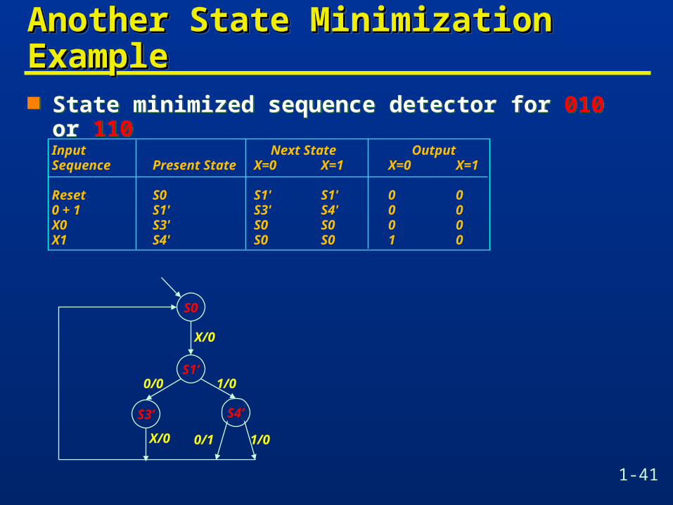
Another State Minimization ExampleAnother State Minimization ExampleAnother State Minimization ExampleAnother State Minimization Example
State minimized sequence detector for 010 or 110 State minimized sequence detector for 010 or 110
Input Next State OutputSequence Present State X=0 X=1 X=0 X=1
Reset S0 S1' S1' 0 00 + 1 S1' S3' S4' 0 0X0 S3' S0 S0 0 0X1 S4' S0 S0 1 0
S0
S1’
S3’ S4’
X/0
1/0
1/00/1
0/0
X/0
1-42
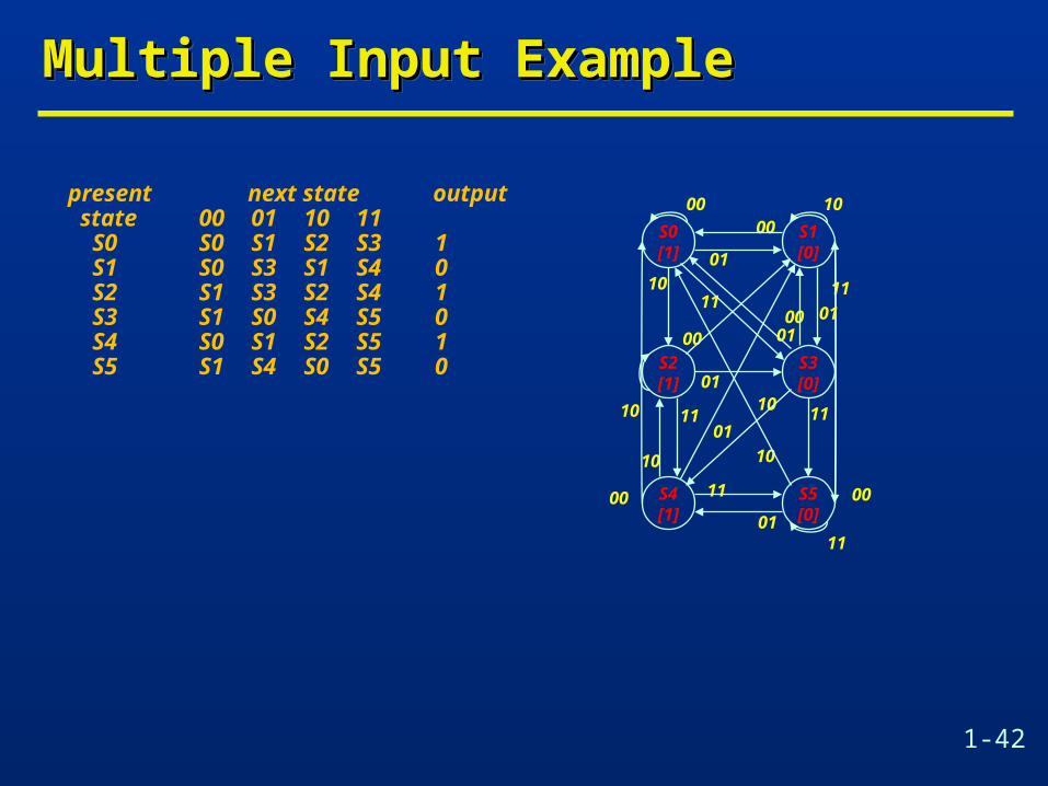
Multiple Input ExampleMultiple Input ExampleMultiple Input ExampleMultiple Input Example
present next state output state 00 01 10 11 S0 S0 S1 S2 S3 1 S1 S0 S3 S1 S4 0 S2 S1 S3 S2 S4 1 S3 S1 S0 S4 S5 0 S4 S0 S1 S2 S5 1 S5 S1 S4 S0 S5 0
1001
11
00
00
01
1110
10
01
1100
1000
11
00
1110
01
10
1101
00
S0[1]
S2[1]
S4[1]
S1[0]
S3[0]
S5[0]
01
1-43
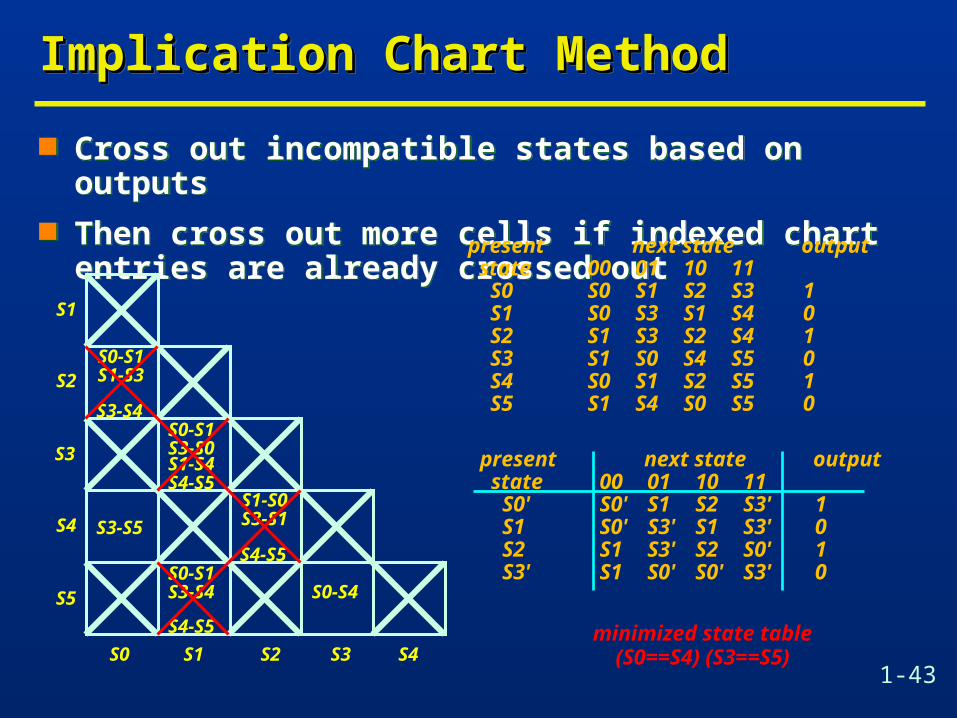
Implication Chart MethodImplication Chart MethodImplication Chart MethodImplication Chart Method
Cross out incompatible states based on outputs Then cross out more cells if indexed chart entries are
already crossed out
Cross out incompatible states based on outputs Then cross out more cells if indexed chart entries are
already crossed out
S0-S1 S1-S3
S3-S4
S3-S5
S0-S1 S3-S0 S1-S4 S4-S5
S0-S1 S3-S4
S4-S5
S1-S0 S3-S1
S4-S5
S0-S4
S1
S2
S3
S4
S5
S0 S1 S2 S3 S4minimized state table
(S0==S4) (S3==S5)
present next state output state 00 01 10 11 S0' S0' S1 S2 S3' 1 S1 S0' S3' S1 S3' 0 S2 S1 S3' S2 S0' 1 S3' S1 S0' S0' S3' 0
present next state output state 00 01 10 11 S0 S0 S1 S2 S3 1 S1 S0 S3 S1 S4 0 S2 S1 S3 S2 S4 1 S3 S1 S0 S4 S5 0 S4 S0 S1 S2 S5 1 S5 S1 S4 S0 S5 0
1-44
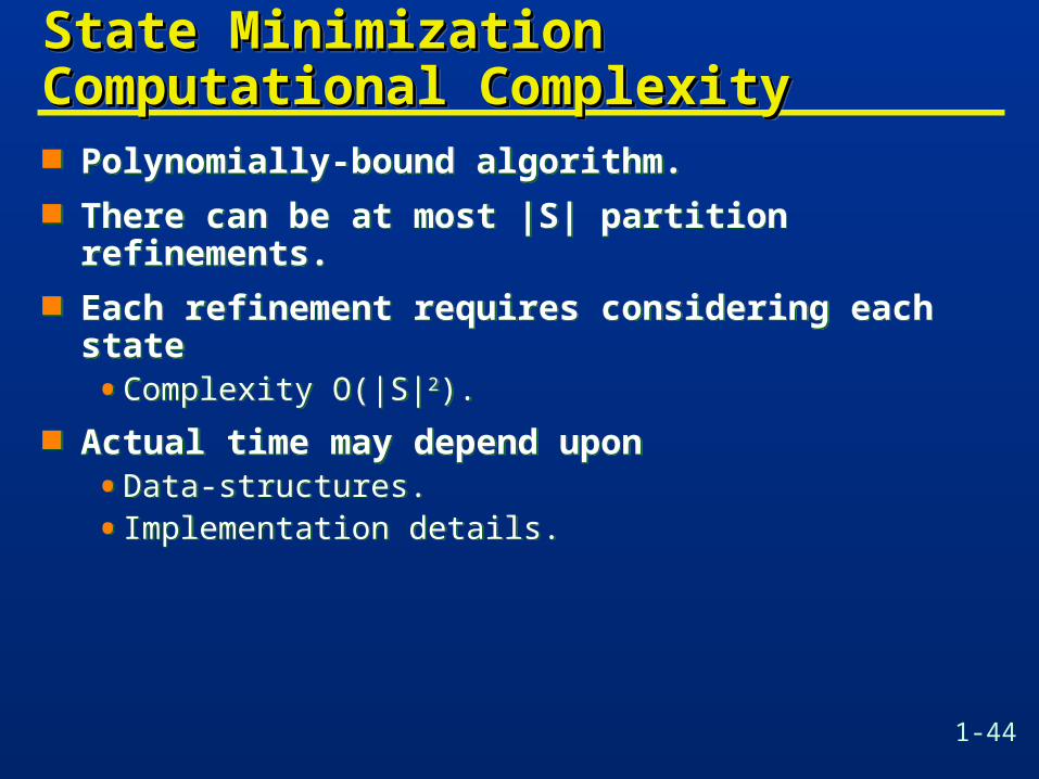
State Minimization Computational State Minimization Computational ComplexityComplexityState Minimization Computational State Minimization Computational ComplexityComplexity Polynomially-bound algorithm. There can be at most |S| partition refinements. Each refinement requires considering each state
• Complexity O(|S|2).
Actual time may depend upon• Data-structures.
• Implementation details.
Polynomially-bound algorithm. There can be at most |S| partition refinements. Each refinement requires considering each state
• Complexity O(|S|2).
Actual time may depend upon• Data-structures.
• Implementation details.
1-45
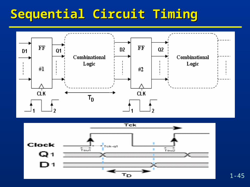
Sequential Circuit TimingSequential Circuit TimingSequential Circuit TimingSequential Circuit Timing
1-46
Timing ConstraintsTiming ConstraintsTiming ConstraintsTiming Constraints
TD = worst case delay through combinational logic
TSU = FF set up time – Minimum time before the clock edge where the input data must be ready and stable
TclkQ = Clock to Q delay – Time between clock edge and data appearing at the output of the FF
THold = FF hold time – Minimum time after the clock edge where data has to remain stable (held stable)
Based on the FF & combinational logic timing parameters, the following timing constraints are obtained for correct operation of the circuit: Tclk ≥ Tclkq1 + TD + Tsu
1-47
Timing ConstraintsTiming ConstraintsTiming ConstraintsTiming Constraints
The previous equation assumes that the clock arrives at all FFs, at exactly the same time!
Clock Skew (Tskew) is the delay between clocks at different chip locations.
To take Clock Skew into account: Tclk ≥ Tclkq1
+ TD + Tsu
+ Tskew
Clock Signals will have random variations in their Periods and Frequencies, called Jitter.
The latest arrival time minus the earliest arrival time during an observed period of time is called the "peak to peak jitter amplitude".
We have to take the Peak to Peak Jitter (TP-P Jitter) into account
Tclk ≥ T clkq1
+ TD + Tsu
+ Tskew + TP-P Jitter
1-48
Timing ConstraintsTiming ConstraintsTiming ConstraintsTiming Constraints
Another Timing Constraint arises in situations where TD is "Zero" or very small when the output of a FF is fed directly to the input of another (e.g. in Shift Registers).
In such situation, we need to make sure that the data does not pass through two FFs (during the transparency window of the FF where both master and slave are enabled).
Hence to avoid Hold Time violation:
Tskew + TP-P Jitter + Thold2 ≤ Tckq1 + TD
where Thold2 is the hold time of the 2nd FF
1-49
MetastabilityMetastabilityMetastabilityMetastability
Whenever there are setup and hold time violations in any flip-flop, it enters a state where its output is unpredictable: this state is known as metastable state (quasi stable state)
At the end of metastable state, the flip-flop settles down to either '1' or '0'. This whole process is known as metastability.
When a flip-flop is in metastable state, its output oscillates between '0' and '1‘. How long it takes to settle down, depends on the technology of the flip-flop.
Metastability occurs when the input signal is an asynchronous signal.
1-50
MetastabilityMetastabilityMetastabilityMetastability
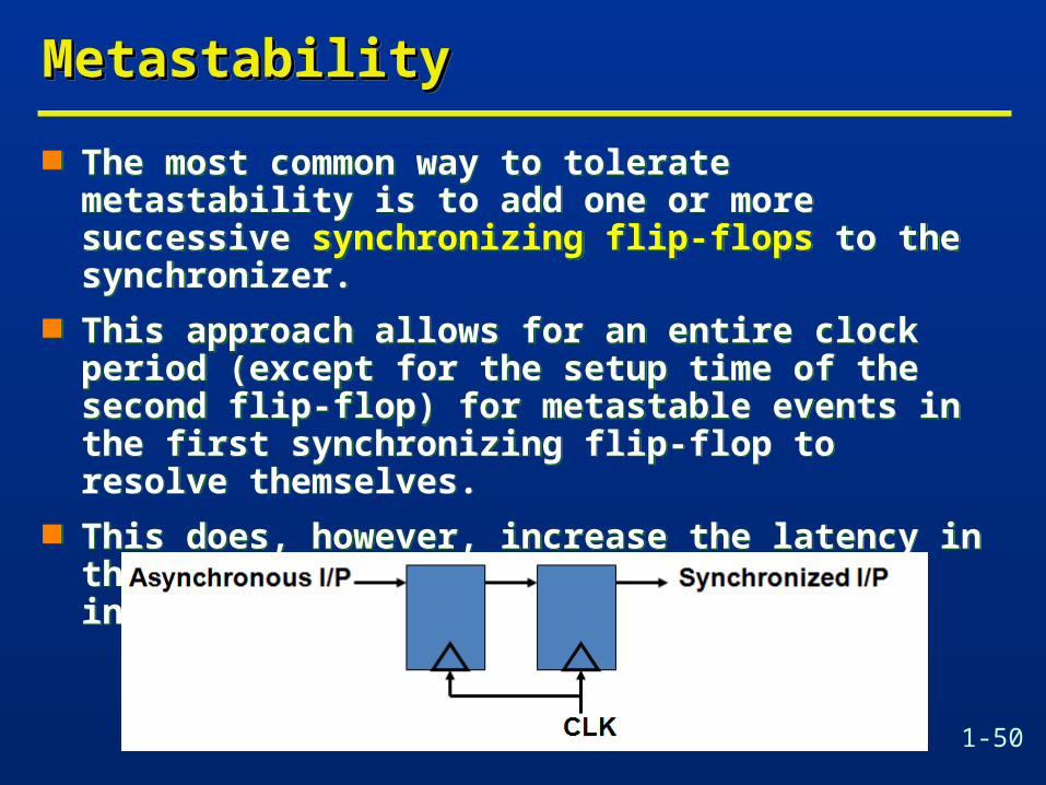
The most common way to tolerate metastability is to add one or more successive synchronizing flip-flops to the synchronizer.
This approach allows for an entire clock period (except for the setup time of the second flip-flop) for metastable events in the first synchronizing flip-flop to resolve themselves.
This does, however, increase the latency in the synchronous logic's observation of input changes.