colibri carrier board design guide - docs.toradex.com · colibri carrier board design guide toradex...
TRANSCRIPT

Colibri Computer Module
Carrier Board Design Guide

Colibri Carrier Board Design Guide
Toradex AG l Altsagenstrasse 5 l 6048 Horw l Switzerland l +41 41 500 48 00 l www.toradex.com l [email protected] Page | 2
Issued by: Toradex Document Type: Carrier Board Design Guide
Purpose: This document is a guideline for developing a carrier board that confirms to the specifications
for the Colibri Computer Module
Document
Version:
1.5
Revision History
Date
Version Remarks
13 April 2015 V1.0 Initial Release: Preliminary Version
28 Sept 2015 V1.1 Correct figure 3 and figure 4 in section 2.3.2 (positive and negative USB
signals were swapped in schematics)
22 October 2015 V1.2 Corrections in figure 4 in section 2.3.2 (pull up resistor of USB_OC# and
pull down of USBH_EN where swapped)
Correction in typical pull up value for I2C in section 2.9
15 June 2016 V1.3 Add section 2.1.4 “Pin Reset State”
Section 2.16: Updated information to input voltage range
Section 2.17: Add note to the usage of PXA270
Section 3.1.3: insert information to nVDD_FAULT, nGPIO_RESET, and
nBATT_SENSE
Section 3.5: Add information to bulk capacitors.
06 April 2017 V1.4 Section 2.2, Ethernet: Minor correction in figure 2
Section 2.5, HDMI/DVI: Correction in figure 12 (differential pair
impedance value)
All reference schematic images: Cosmetic update.
Section 1.2, Section 4 & Section 5: Updated web-links
14 Dec 2018 V1.5 Section 2.2.2: Add recommendation for ESD protection diodes
Section 2.3.1: Add note regarding default polarity of USB_H_PWR_EN
Section 2.3.2: Add USB OTG reference schematic
Section 2.3.2: Remove 15k pull down on USB data signals
Section 2.3.2.3: Change to active low version of power switch (TPS2042
instead of TPS2052)
Section 2.15.3: Update recommendation for unused touch signals
Section 2.16.1: Correct pin numbers

Colibri Carrier Board Design Guide
Toradex AG l Altsagenstrasse 5 l 6048 Horw l Switzerland l +41 41 500 48 00 l www.toradex.com l [email protected] Page | 3
1 Introduction ....................................................................................................................... 5 1.1 Overview ............................................................................................................................. 5 1.2 Additional Documents .......................................................................................................... 5
1.2.1 Layout Design Guide ................................................................................................. 5 1.2.2 Colibri Module Datasheets ......................................................................................... 5 1.2.3 Toradex Developer Centre ......................................................................................... 5 1.2.4 Colibri Evaluation Board Schematics .......................................................................... 5 1.2.5 Pinout Designer ........................................................................................................ 6
1.3 Abbreviations ....................................................................................................................... 6
2 Interfaces ........................................................................................................................... 8 2.1 Architecture ......................................................................................................................... 8
2.1.1 Standard Interfaces ................................................................................................... 8 2.1.2 Interfaces on Alternative Functions ............................................................................. 8 2.1.3 Pin Numbering .......................................................................................................... 9 2.1.4 Pin Reset State ......................................................................................................... 9
2.2 Ethernet ............................................................................................................................ 10 2.2.1 Ethernet Signals ...................................................................................................... 10 2.2.2 Reference Schematics ............................................................................................. 10 2.2.3 Unused Ethernet Signals Termination ....................................................................... 11
2.3 USB .................................................................................................................................. 11 2.3.1 USB Signals ........................................................................................................... 11 2.3.2 Reference Schematics ............................................................................................. 12 2.3.3 Unused USB Signal Termination .............................................................................. 13
2.4 Parallel RGB LCD Interface ................................................................................................ 14 2.4.1 Parallel RGB LCD Signals ....................................................................................... 14 2.4.2 Reference Schematics ............................................................................................. 14 2.4.3 Unused Parallel RGB Interface Signal Termination .................................................... 17
2.5 HDMI/DVI .......................................................................................................................... 18 2.5.1 HDMI/DVI Signals ................................................................................................... 18 2.5.2 Reference Schematics ............................................................................................. 18 2.5.3 Unused HDMI/DVI Signal Termination ...................................................................... 20
2.6 Analogue VGA ................................................................................................................... 21 2.6.1 VGA Signals ........................................................................................................... 21 2.6.2 Reference Schematics ............................................................................................. 21 2.6.3 Unused VGA Interface Signal Termination ................................................................ 22
2.7 Parallel Camera Interface ................................................................................................... 22 2.7.1 Parallel Camera Signals .......................................................................................... 22 2.7.2 Unused Parallel Camera Interface Signal Termination ............................................... 23
2.8 SD/MMC/SDIO .................................................................................................................. 23 2.8.1 SD/MMC/SDIO Signals ............................................................................................ 23 2.8.2 Reference Schematics ............................................................................................. 24 2.8.3 Unused SD/MMC/SDIO Interface Signal Termination ................................................. 24
2.9 I2C .................................................................................................................................... 24 2.9.1 I2C Signals .............................................................................................................. 24 2.9.2 Real-Team Clock (RTC) recommendation ................................................................. 24 2.9.3 Unused I2C Signal Termination ................................................................................. 25
2.10 UART ................................................................................................................................ 25 2.10.1 UART Signals ...................................................................................................... 25 2.10.2 Reference Schematics ......................................................................................... 26 2.10.3 Unused UART Signal Termination ......................................................................... 27
2.11 SPI ................................................................................................................................... 28 2.11.1 SPI Signals .......................................................................................................... 28 2.11.2 Unused SPI Signal Termination ............................................................................ 28
2.12 CAN .................................................................................................................................. 28 2.12.1 Reference Schematics ......................................................................................... 28
2.13 PWM ................................................................................................................................. 29

Colibri Carrier Board Design Guide
Toradex AG l Altsagenstrasse 5 l 6048 Horw l Switzerland l +41 41 500 48 00 l www.toradex.com l [email protected] Page | 4
2.13.1 PWM Signals ....................................................................................................... 29 2.13.2 Reference Schematics ......................................................................................... 29 2.13.3 Unused PWM Signal Termination .......................................................................... 29
2.14 Analogue Audio ................................................................................................................. 30 2.14.1 Analogue Audio Signals ....................................................................................... 30 2.14.2 Reference Schematics ......................................................................................... 30 2.14.3 Unused Analogue Audio Signal Termination .......................................................... 31
2.15 Touch Panel Interface ........................................................................................................ 32 2.15.1 Resistive Touch Signals ....................................................................................... 32 2.15.2 Reference Schematics ......................................................................................... 32 2.15.3 Unused Touch Panel Interface Signal Termination ................................................. 32
2.16 Analogue Inputs ................................................................................................................. 33 2.16.1 Analogue Input Signals ......................................................................................... 33 2.16.2 Unused Analogue Inputs Signal Termination .......................................................... 33
2.17 Parallel Memory Bus (External Memory Bus) ....................................................................... 33 2.17.1 Memory Bus Signals ............................................................................................ 33 2.17.2 Unused Memory Bus Signals Termination ............................................................. 35
2.18 GPIO ................................................................................................................................ 35 2.18.1 Preferred GPIO Signals ........................................................................................ 35 2.18.2 Unused GPIO Termination .................................................................................... 35
3 Power Management ........................................................................................................... 36 3.1 Power Signals ................................................................................................................... 36
3.1.1 Digital Supply Signals .............................................................................................. 36 3.1.2 Analogue Supply Signals ......................................................................................... 36 3.1.3 Power Management Signals .................................................................................... 36
3.2 Power Block Diagram ......................................................................................................... 37 3.3 Power States ..................................................................................................................... 39 3.4 Power-Up Sequence .......................................................................................................... 39 3.5 Reference Schematics ....................................................................................................... 40
4 Mechanical and Thermal Consideration ............................................................................... 42 4.1 Module Connector.............................................................................................................. 42 4.2 Fixation of the Module ........................................................................................................ 42 4.3 Thermal Solution ................................................................................................................ 44 4.4 Module Size ...................................................................................................................... 44
5 Appendix A – Physical Pin Definition and Location ............................................................... 45

Colibri Carrier Board Design Guide
Toradex AG l Altsagenstrasse 5 l 6048 Horw l Switzerland l +41 41 500 48 00 l www.toradex.com l [email protected] Page | 5
1 Introduction
1.1 Overview
This document guides the development of a customized carrier board for the Colibri computer
module. It describes the different interfaces and contains reference schematics. This document
reflects only the standardized primary function of the Colibri modules. The alternative functions are
not guaranteed to be compatible between different Colibri modules. These interfaces are described
in the datasheet of each computer module. Some Colibri modules do not feature the full set of
standard interfaces. Therefore, it is strongly recommended to read the datasheets of the modules
that are intended to be used with the carrier board.
Some of the Colibri computer module interfaces such as High-Speed USB, Ethernet, etc. require
special layout considerations regarding trace impedance and length matching. Please carefully
read the Toradex Layout Design Guide for additional information related to the routing of these
interfaces.
1.2 Additional Documents
1.2.1 Layout Design Guide
This document contains layout requirement specifications for the high-speed signals and helps in
avoiding problems related to the layout.
http://developer.toradex.com/carrier-board-design/carrier-board-design-guides
1.2.2 Colibri Module Datasheets
There is a datasheet available for every Colibri module. Amongst other things, this document
describes the type-specific interfaces and the alternative function of the pins. Before starting the
development of a customized carrier board, please check this document to find out whether the
required interfaces are really available on the selected modules.
https://www.toradex.com/computer-on-modules/colibri-arm-family
1.2.3 Toradex Developer Centre
You can find a lot of additional information at the Toradex Developer Centre, which is updated
with the latest product support information on a regular basis.
Please note that the Developer Centre is common for all Toradex products. You should always
check to ensure if the information is valid or relevant for the specific Colibri modules.
http://www.developer.toradex.com
1.2.4 Colibri Evaluation Board Schematics
We provide the complete schematics plus the Altium project file for the Colibri Evaluation Board for
free. This is a great help when designing your own Carrier Board.
http://developer.toradex.com/products/colibri-evaluation-board

Colibri Carrier Board Design Guide
Toradex AG l Altsagenstrasse 5 l 6048 Horw l Switzerland l +41 41 500 48 00 l www.toradex.com l [email protected] Page | 6
1.2.5 Pinout Designer
This is an interactive and useful tool for configuring the pin muxing of the Colibri and Apalis
modules. It can be really helpful in custom carrier board development on Toradex modules and for
checking the compatibility of existing carrier boards with our modules.
http://developer.toradex.com/carrier-board-design/pinout-designer-tool
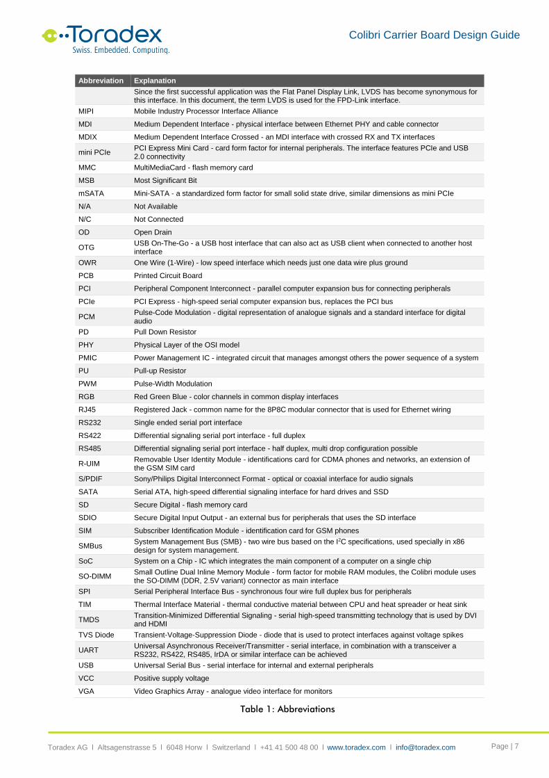
1.3 Abbreviations
Abbreviation Explanation
ADC Analogue to Digital Converter
AGND Analogue Ground - separate ground for analogue signals
Auto-MDIX Automatically Medium Dependent Interface Crossing - a PHY with Auto-MDIX f is able to detect whether RX and TX need to be crossed (MDI or MDIX)
CAD Computer-Aided Design - in this document is referred to PCB Layout tools
CAN Controller Area Network - a bus that is manly used in automotive and industrial environment
CDMA Code Division Multiplex Access - abbreviation often used for a mobile phone standard for data communication
CEC Consumer Electronic Control - HDMI feature that allows to control CEC compatible devices
CPU Central Processor Unit
CSI Camera Serial Interface
DAC Digital to Analogue Converter
DDC Display Data Channel - interface for reading out the capability of a monitor, in this document DDC2B (based on I2C) is always meant
DRC Design Rule Check - a tool for checking whether all design rules are satisfied in a CAD tool
DSI Display Serial Interface
DVI Digital Visual Interface - digital signals are electrical compatible with HDMI
DVI-A Digital Visual Interface Analogue only - signals are compatible with VGA
DVI-D Digital Visual Interface Digital only - signals are electrical compatible with HDMI
DVI-I Digital Visual Interface Integrated - combines digital and analogue video signals in one connector
EDA Electronic Design Automation - software for schematic capture and PCB layout (CAD or ECAD)
EDID Extended Display Identification Data - timing setting information provided by the display in a PROM
EMI Electromagnetic Interference - high frequency disturbances
eMMC Embedded Multi Media Card - flash memory combined with MMC interface controller in a BGA package, used as internal flash memory
ESD Electrostatic Discharge - high voltage spike or spark that can damage electrostatic- sensitive devices
FPD-Link Flat Panel Display Link - high-speed serial interface for liquid crystal displays. In this document also called LVDS interface.
GBE Gigabit Ethernet - Ethernet interface with a maximum data rate of 1000Mbit/s
GND Ground
GPIO General Purpose Input/Output pin that can be configured to be either an input or output
GSM Global System for Mobile Communications
HDA High Definition Audio (HD Audio) - digital audio interface between CPU and audio codec
HDCP High-Bandwidth Digital Content Protection - copy protection system that is used by HDMI beside others
HDMI High-Definition Multimedia Interface - combines audio and video signal for connecting monitors, TV sets or Projectors, electrical compatible with DVI-D
I2C Inter-Integrated Circuit - two wire interface for connecting low speed peripherals
I2S Integrated Interchip Sound - serial bus for connecting PCM audio data between two devices
IrDA Infrared Data Association - infrared interface for connecting peripherals
JTAG Joint Test Action Group - widely used debug interface
LCD Liquid Crystal Display
LSB Least Significant Bit
LVDS Low-Voltage Differential Signaling - electrical interface standard that can transport very high-speed signals over twisted-pair cables. Many standard interfaces like PCIe or SATA use this interface standard.
Colibri Carrier Board Design Guide
Toradex AG l Altsagenstrasse 5 l 6048 Horw l Switzerland l +41 41 500 48 00 l www.toradex.com l [email protected] Page | 7
Abbreviation Explanation
Since the first successful application was the Flat Panel Display Link, LVDS has become synonymous for this interface. In this document, the term LVDS is used for the FPD-Link interface.
MIPI Mobile Industry Processor Interface Alliance
MDI Medium Dependent Interface - physical interface between Ethernet PHY and cable connector
MDIX Medium Dependent Interface Crossed - an MDI interface with crossed RX and TX interfaces
mini PCIe PCI Express Mini Card - card form factor for internal peripherals. The interface features PCIe and USB 2.0 connectivity
MMC MultiMediaCard - flash memory card
MSB Most Significant Bit
mSATA Mini-SATA - a standardized form factor for small solid state drive, similar dimensions as mini PCIe
N/A Not Available
N/C Not Connected
OD Open Drain
OTG USB On-The-Go - a USB host interface that can also act as USB client when connected to another host interface
OWR One Wire (1-Wire) - low speed interface which needs just one data wire plus ground
PCB Printed Circuit Board
PCI Peripheral Component Interconnect - parallel computer expansion bus for connecting peripherals
PCIe PCI Express - high-speed serial computer expansion bus, replaces the PCI bus
PCM Pulse-Code Modulation - digital representation of analogue signals and a standard interface for digital audio
PD Pull Down Resistor
PHY Physical Layer of the OSI model
PMIC Power Management IC - integrated circuit that manages amongst others the power sequence of a system
PU Pull-up Resistor
PWM Pulse-Width Modulation
RGB Red Green Blue - color channels in common display interfaces
RJ45 Registered Jack - common name for the 8P8C modular connector that is used for Ethernet wiring
RS232 Single ended serial port interface
RS422 Differential signaling serial port interface - full duplex
RS485 Differential signaling serial port interface - half duplex, multi drop configuration possible
R-UIM Removable User Identity Module - identifications card for CDMA phones and networks, an extension of the GSM SIM card
S/PDIF Sony/Philips Digital Interconnect Format - optical or coaxial interface for audio signals
SATA Serial ATA, high-speed differential signaling interface for hard drives and SSD
SD Secure Digital - flash memory card
SDIO Secure Digital Input Output - an external bus for peripherals that uses the SD interface
SIM Subscriber Identification Module - identification card for GSM phones
SMBus System Management Bus (SMB) - two wire bus based on the I2C specifications, used specially in x86 design for system management.
SoC System on a Chip - IC which integrates the main component of a computer on a single chip
SO-DIMM Small Outline Dual Inline Memory Module - form factor for mobile RAM modules, the Colibri module uses the SO-DIMM (DDR, 2.5V variant) connector as main interface
SPI Serial Peripheral Interface Bus - synchronous four wire full duplex bus for peripherals
TIM Thermal Interface Material - thermal conductive material between CPU and heat spreader or heat sink
TMDS Transition-Minimized Differential Signaling - serial high-speed transmitting technology that is used by DVI and HDMI
TVS Diode Transient-Voltage-Suppression Diode - diode that is used to protect interfaces against voltage spikes
UART Universal Asynchronous Receiver/Transmitter - serial interface, in combination with a transceiver a RS232, RS422, RS485, IrDA or similar interface can be achieved
USB Universal Serial Bus - serial interface for internal and external peripherals
VCC Positive supply voltage
VGA Video Graphics Array - analogue video interface for monitors
Table 1: Abbreviations
Colibri Carrier Board Design Guide
Toradex AG l Altsagenstrasse 5 l 6048 Horw l Switzerland l +41 41 500 48 00 l www.toradex.com l [email protected] Page | 8
2 Interfaces
2.1 Architecture
2.1.1 Standard Interfaces
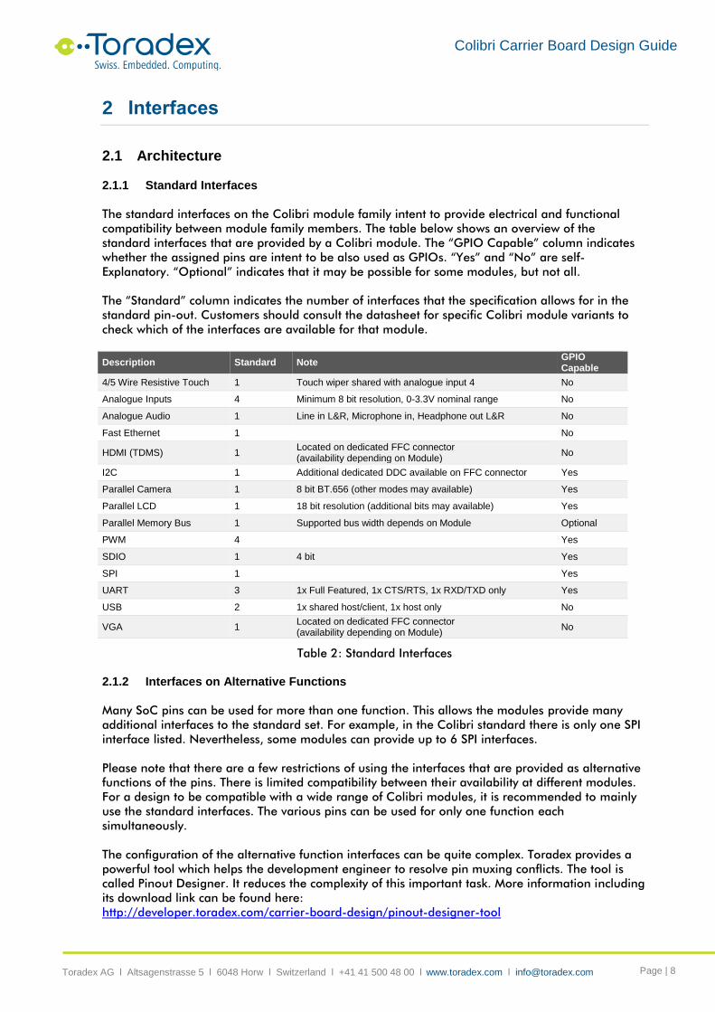
The standard interfaces on the Colibri module family intent to provide electrical and functional
compatibility between module family members. The table below shows an overview of the
standard interfaces that are provided by a Colibri module. The “GPIO Capable” column indicates
whether the assigned pins are intent to be also used as GPIOs. “Yes” and “No” are self-
Explanatory. “Optional” indicates that it may be possible for some modules, but not all.
The “Standard” column indicates the number of interfaces that the specification allows for in the
standard pin-out. Customers should consult the datasheet for specific Colibri module variants to
check which of the interfaces are available for that module.
Description Standard Note GPIO Capable
4/5 Wire Resistive Touch 1 Touch wiper shared with analogue input 4 No
Analogue Inputs 4 Minimum 8 bit resolution, 0-3.3V nominal range No
Analogue Audio 1 Line in L&R, Microphone in, Headphone out L&R No
Fast Ethernet 1 No
HDMI (TDMS) 1 Located on dedicated FFC connector (availability depending on Module)
No
I2C 1 Additional dedicated DDC available on FFC connector Yes
Parallel Camera 1 8 bit BT.656 (other modes may available) Yes
Parallel LCD 1 18 bit resolution (additional bits may available) Yes
Parallel Memory Bus 1 Supported bus width depends on Module Optional
PWM 4 Yes
SDIO 1 4 bit Yes
SPI 1 Yes
UART 3 1x Full Featured, 1x CTS/RTS, 1x RXD/TXD only Yes
USB 2 1x shared host/client, 1x host only No
VGA 1 Located on dedicated FFC connector (availability depending on Module)
No
Table 2: Standard Interfaces
2.1.2 Interfaces on Alternative Functions
Many SoC pins can be used for more than one function. This allows the modules provide many
additional interfaces to the standard set. For example, in the Colibri standard there is only one SPI
interface listed. Nevertheless, some modules can provide up to 6 SPI interfaces.
Please note that there are a few restrictions of using the interfaces that are provided as alternative
functions of the pins. There is limited compatibility between their availability at different modules.
For a design to be compatible with a wide range of Colibri modules, it is recommended to mainly
use the standard interfaces. The various pins can be used for only one function each
simultaneously.
The configuration of the alternative function interfaces can be quite complex. Toradex provides a
powerful tool which helps the development engineer to resolve pin muxing conflicts. The tool is
called Pinout Designer. It reduces the complexity of this important task. More information including
its download link can be found here:
http://developer.toradex.com/carrier-board-design/pinout-designer-tool

Colibri Carrier Board Design Guide
Toradex AG l Altsagenstrasse 5 l 6048 Horw l Switzerland l +41 41 500 48 00 l www.toradex.com l [email protected] Page | 9
The interfaces on the alternative functions are not described in this document since they differ
between the modules. Information related to these functions can be found in the datasheets of the
modules.
2.1.3 Pin Numbering
The diagrams in the figures below show the pin numbering schema on both sides of the module.
The schema is equals to the JEDEC MO-224 DDR SO-DIMM standard. The odd pin numbers are
located on the top side of the module.
Figure 1: Colibri Module Pin Numbering Schema
2.1.4 Pin Reset State
The datasheets of the Colibri module provide information about the default reset status of the IO
pins. Please be aware, the pin reset status is only guaranteed during the release of the reset
signal. Some of the modules switches the IO bank voltages in order to follow the power up
sequence of the SoC. This means, the IO pins can have an undefined state between applying the
main power to the module until the nRESET_OUT is released. For carrier board designs that do not
allow undefined pin states, it is recommended to make sure that the peripheral devices are not
getting powered before the nRESET_OUT is released. Another solution can be gating the according
IO signals with the nRESET_OUT signal.
Pin1 Pin47Pin39 Pin199
Pin2 Pin42Pin40 Pin200

Colibri Carrier Board Design Guide
Toradex AG l Altsagenstrasse 5 l 6048 Horw l Switzerland l +41 41 500 48 00 l www.toradex.com l [email protected] Page | 10
2.2 Ethernet
The Colibri module standard features a fast 10/100Mbit Ethernet (10/100Base-TX) interface port.
The required center tap circuit can differ between the modules. Different assembly options might
be needed for supporting the complete Colibri module family. Some modules support Auto MDIX,
which means they can swap the transmitting with the receiving lanes. Read the corresponding
datasheet of the module for more information about the availability of the Auto MDIX function.
2.2.1 Ethernet Signals
Colibri Pin
Colibri Signal Name
I/O Type Power Rail
Description
189 ETH_1_TXO+ I Analogue 100BASE-TX: Transmit + (Auto MDIX: Receive +)
187 ETH_1_TXO- I Analogue 100BASE-TX: Transmit - (Auto MDIX: Receive -)
195 ETH_1_RXI+ O Analogue 100BASE-TX: Receive + (Auto MDIX: Transmit +)
193 ETH_1_RXI- O Analogue 100BASE-TX: Receive - (Auto MDIX: Transmit -)
191 AGND_LAN Ethernet ground, on some modules connected to common GND
183 ETH_1_LINK_AKT O CMOS 3.3V LED indication output for link activity on the Ethernet port
185 ETH_1_SPEED100 O CMOS 3.3V LED indication output for 100Mbit/s
Table 3: Ethernet Signals
2.2.2 Reference Schematics
Ethernet connectors with integrated magnetics are preferable. If a design with external magnetics
is chosen, additional care has to be taken to route the signals between the magnetics and Ethernet
connector.
The LED output signals ETH_1_LINK_AKT and ETH_1_SPEED100 can be connected directly to the
LED of the Ethernet jack with suitable serial resistors. There is no need for additional buffering if
the current drawn does not exceeds 10mA.
The Fast Ethernet interface uses the ETH_1_TXO as transmitting lanes and the ETH_1_RXI as
receiving lane. If the Ethernet PHY features Auto-MDIX, the signal lanes RX and TX could be
swapped. We strongly recommend not swapping the RX and TX lanes in order to keep the
compatibility with all Colibri modules.
The required center tap circuit depends on the supported modules. Currently, the Ethernet
controller on the PXA270 module is the only one which requires a different center tap circuit since
it does not support Auto-MDIX. All the other currently available modules feature a current control
PHY which requires 3.3V supply at the center tap of the RX and TX lanes. Since all the Ethernet PHY
manufacturer are tending to change from current mode to voltage mode which requires leaving
the center tab pins of the magnetics unconnected, we recommend to add additional 0R resistors
into the center tab lines. This ensures that the carrier board design is ready for any future Colibri
module with voltage mode PHY.
The magnetics provide a certain ESD protection which is sufficient for many designs. However,
especially in Power over Ethernet (PoE) systems, additional transient voltage suppressor diodes
(TVS) are highly recommended to be placed between the module and the magnetics. More
information can be found in the following application note from Microchip:
http://ww1.microchip.com/downloads/en/AppNotes/00002157B.pdf

Colibri Carrier Board Design Guide
Toradex AG l Altsagenstrasse 5 l 6048 Horw l Switzerland l +41 41 500 48 00 l www.toradex.com l [email protected] Page | 11
Figure 2: Fast Ethernet with Integrated Magnetics Reference Schematic
2.2.3 Unused Ethernet Signals Termination
All unused Ethernet signals can be left unconnected.
2.3 USB
The Colibri modules feature two USB interfaces. One of the two USB interfaces can be configured
to be used as either the host or client. The other interface can only be used as host. Some of the
Colibri modules use the USB client port for debugging and recovery purpose. Therefore, it is
recommended to have the interface accessible even for carrier board designs which do not need
any USB ports.
2.3.1 USB Signals
Colibri Pin
Colibri Signal Name
I/O Type Power Rail
Description
139 USB_H_DP I/O USB 3.3V Positive Differential Signal for USB Host port
141 USB_H_DM I/O USB 3.3V Negative Differential Signal for USB Host port
143 USB_C_DP I/O USB 3.3V Positive Differential Signal for the shared USB Host / Client port
145 USB_C_DM I/O USB 3.3V Negative Differential Signal for the shared USB Host / Client port
Table 4: USB Data Signals
If you use the USB Host function you need to generate the 5V USB supply voltage on your carrier
board. The Colibri modules provide two optional signals for USB power supply control (PWR_EN
and OC). We recommend using the following pins to ensure the best possible compatibility.
However, use of these signals is not mandatory and other GPIOs may be used instead.
In the USB client mode, an additional signal is required that detects whether the client is connected
to a host interface (VBUS_DETECT). Please note that this pin is only 3.3V tolerant. Therefore, an
additional logic level shifter (simplest solution is a voltage divider) is required.
Colibri Pin
Colibri Signal Name
I/O Type Power Rail
Description
129 USB_H_PWR_EN O CMOS 3.3V This pin enables the external USB voltage supply. By default, this pin is active low.
131 USB_H_OC I CMOS 3.3V USB overcurrent, this pin can signal an over current condition in the USB supply
137 USB_C_VBUS_DETECT I CMOS 3.3V Use this pin to detect if VBUS is present (5V USB supply). Please note that this pin is only 3.3V tolerant
Table 5: USB Control Signals
ETH_LINK_ACT
ETH_SPEED
ETH_TX 0_N
ETH_TX 0_P
ETHERNET[0..5]
50R
R20
50R
R21
100nF
16VC45GND
50R
R22
50R
R23
100nF
16VC46GND
ETH_RX I_P
ETH_RX I_N
C44
100nF
16V
GND
ETH_AVCC
3.3V
3.3V
2A
220R@ 100MHz
L10
47uF
6.3V
+
C4 8
47uF
6.3V
+
C49
3.3V ETH_AVCC
GND
150 RR25
150RR24
J00- 0065N L
TD +1
TD -2
CT_TX D4
CT_RX D5
RD +3
RD -6
LED_Left_ A9
LED_Left_ C10
LED_R ight_ C11
LED_R ight_ A12
SHIELDS1
SHIELDS2
NC7
CH S GND8
X17
ETH_LINK_ACT
ETH_SPEED
ETH_TX0_N
ETH_TX0_P
ETH_RXI_N
ETH_RXI_P
1473005 -1
ETH_LINK_ACT183
ETH_SPEED185
ETH_TX0-
ETH_TX0+189
ETH_RXI- 193
ETH_RXI+195
ETH_GND191
Colibri - Ethernet
2 of 16
X1B
SHIELD
Ethernet Connector
ETH_CT_TX
ETH_CT_RXGND
GND
0R
R10
C47
100nF
16 V
GND
0R
R11
0R
R12
NA
PXA2700RNA0R
ModuleR12R11R10
All except PXA2700RNA 0R
Reserved for future modulesNA NANA
(Integrated Magnetics)
187
Colibri Carrier Board Design Guide
Toradex AG l Altsagenstrasse 5 l 6048 Horw l Switzerland l +41 41 500 48 00 l www.toradex.com l [email protected] Page | 12
2.3.2 Reference Schematics
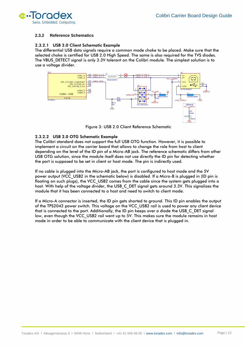
2.3.2.1 USB 2.0 Client Schematic Example
The differential USB data signals require a common mode choke to be placed. Make sure that the
selected choke is certified for USB 2.0 High Speed. The same is also required for the TVS diodes.
The VBUS_DETECT signal is only 3.3V tolerant on the Colibri module. The simplest solution is to
use a voltage divider.
Figure 3: USB 2.0 Client Reference Schematic
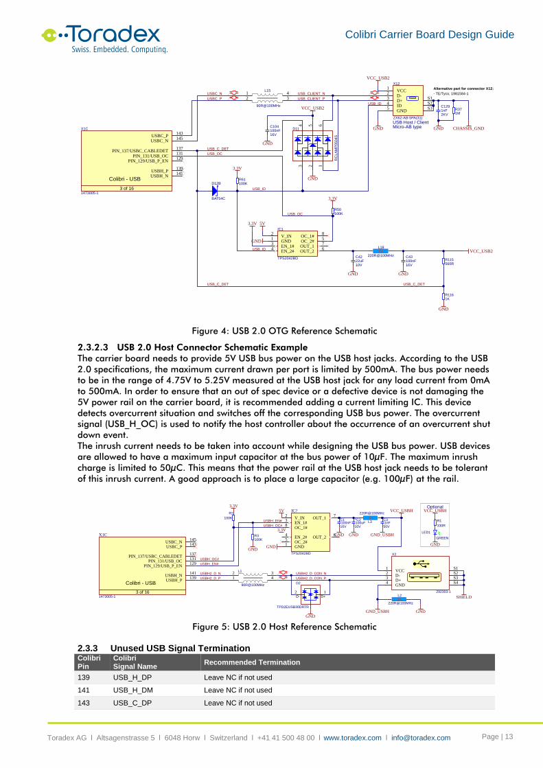
2.3.2.2 USB 2.0 OTG Schematic Example
The Colibri standard does not support the full USB OTG function. However, it is possible to
implement a circuit on the carrier board that allows to change the role from host to client
depending on the level of the ID pin of a Micro-AB jack. The reference schematic differs from other
USB OTG solution, since the module itself does not use directly the ID pin for detecting whether
the port is supposed to be set in client or host mode. The pin is indirectly used.
If no cable is plugged into the Micro-AB jack, the port is configured to host mode and the 5V
power output (VCC_USB2 in the schematic below) is disabled. If a Micro-B is plugged in (ID pin is
floating on such plugs), the VCC_USB2 comes from the cable since the system gets plugged into a
host. With help of the voltage divider, the USB_C_DET signal gets around 3.3V. This signalizes the
module that it has been connected to a host and need to switch to client mode.
If a Micro-A connector is inserted, the ID pin gets shorted to ground. This ID pin enables the output
of the TPS2042 power switch. This voltage on the VCC_USB2 rail is used to power any client device
that is connected to the port. Additionally, the ID pin keeps over a diode the USB_C_DET signal
low, even though the VCC_USB2 rail went up to 5V. This makes sure the module remains in host
mode in order to be able to communicate with the client device that is plugged in.
GND
2A220R@100MHz
L1
90R@100MHz
12 3
4
L2USBO1_D_N
USBO1_D_P
USBO1_D_CON_N
USBO1_D_CON_P
330R
R3
GND
GREEN
LED1
SHIELD
VCC_USBO1
VCC_USBO1
GND_USBO1
Optional
USBO1_VBUS
RCLAMP0504S
1
2
3 4
5
6
D1
4A39R@100MHz
L3
100nF
C1
SHIELD
5V_ESD
SHIELD
5V
VCC1
D-2
D+3
GND4
S1S2
61729-0010BLF
X2
1473005-1
USBH_P139
USBH_N141
USBC_P143
USBC_N145
PIN_131/USB_OC131
PIN_137/USBC_CABLEDET137
PIN_129/USB_P_EN129
Colibri - USB
3 of 16
X1C
560R
R73
R741K
GND
Colibri Carrier Board Design Guide
Toradex AG l Altsagenstrasse 5 l 6048 Horw l Switzerland l +41 41 500 48 00 l www.toradex.com l [email protected] Page | 13
Figure 4: USB 2.0 OTG Reference Schematic
2.3.2.3 USB 2.0 Host Connector Schematic Example
The carrier board needs to provide 5V USB bus power on the USB host jacks. According to the USB
2.0 specifications, the maximum current drawn per port is limited by 500mA. The bus power needs
to be in the range of 4.75V to 5.25V measured at the USB host jack for any load current from 0mA
to 500mA. In order to ensure that an out of spec device or a defective device is not damaging the
5V power rail on the carrier board, it is recommended adding a current limiting IC. This device
detects overcurrent situation and switches off the corresponding USB bus power. The overcurrent
signal (USB_H_OC) is used to notify the host controller about the occurrence of an overcurrent shut
down event.
The inrush current needs to be taken into account while designing the USB bus power. USB devices
are allowed to have a maximum input capacitor at the bus power of 10µF. The maximum inrush
charge is limited to 50µC. This means that the power rail at the USB host jack needs to be tolerant
of this inrush current. A good approach is to place a large capacitor (e.g. 100µF) at the rail.
Figure 5: USB 2.0 Host Reference Schematic
2.3.3 Unused USB Signal Termination Colibri Pin
Colibri Signal Name
Recommended Termination
139 USB_H_DP Leave NC if not used
141 USB_H_DM Leave NC if not used
143 USB_C_DP Leave NC if not used
GND
5V
VCC_USB2
R50100K
3.3V
USBC_P
USBC_N
GND
VCC_USB2
90R@100MHz
12 3
4L15
220R@100MHz
2AL18
100nF16V
C43
GND
USB_C_DET
3.3V
USB_ID
R61100K
TPS2042BD
GND1
V_IN2
EN_1#3
EN_2#4
OC_2#5
OUT_26
OUT_17
OC_1#8
IC1
RC
LA
MP
050
4S
1234 5 6
D11100nF16V
C104
560RR115
R1161K
GND
GND
GND
USB_ID
1473005-1
USBH_P139
USBH_N141
USBC_P143
USBC_N145
PIN_131/USB_OC131
PIN_137/USBC_CABLEDET137
PIN_129/USB_P_EN129
Colibri - USB
3 of 16
X1C
USB_CLIENT_N
USB Host / ClientMicro-AB type
22uF10V
C42
VCC_USB2
USB_OC
GND
USB_C_DET
USB_CLIENT_P
BAT54C
D12B
ZX62-AB-5PA(31)
VCC1
D-2
D+3
ID4
GND5
S1
S3S2
X12
Alternative part for connector X12:
- TE/Tyco, 1981584-1
CHASSIS_GND
1nF2KV
C129R371M
GND
USB_OC
USB_ID
USB_C_DET
3.3V
2A
220R@100MHz
L3 1nF50V
C3
GND_USBH
100nF16V
C1
GND
100uF10V
+C2
GND
GND
2A220R@100MHz
L2
90R@100MHz
12 3
4
L1USBH2_D_N
USBH2_D_P
USBH2_D_CON_N
USBH2_D_CON_P
330R
R1
GND
GREEN
LED1
TPD2EUSB30DRTR
12D+D-
D2
GND
SHIELD
VCC_USBH VCC_USBH
USBH_OC#
USBH_EN#
GND_USBH
Optional
USBH_OC#
USBH_EN#
GND
5V
VCC1
D-2
D+3
GND4
292303-1
S1S2S3S4
X2
R2
100K
3.3V
R3100K
GND
1473005-1
USBH_P139
USBH_N141
USBC_P143
USBC_N145
PIN_131/USB_OC131
PIN_137/USBC_CABLEDET137
PIN_129/USB_P_EN129
Colibri - USB
3 of 16
X1C
TPS2042BD
GND1
V_IN2
EN_1#3
EN_2#4
OC_2#5
OUT_26
OUT_17
OC_1#8
IC?
3.3V
Colibri Carrier Board Design Guide
Toradex AG l Altsagenstrasse 5 l 6048 Horw l Switzerland l +41 41 500 48 00 l www.toradex.com l [email protected] Page | 14
Colibri Pin
Colibri Signal Name
Recommended Termination
145 USB_C_DM Leave NC if not used
129 USB_H_PWR_EN Leave NC if not used
131 USB_H_OC Add pull-up resistor or disable the overcurrent function in software
137 USB_C_VBUS_DETECT Leave NC if not used
Table 6: Unused USB Signals Termination
2.4 Parallel RGB LCD Interface
The Colibri modules feature one parallel RGB LCD interface as main display interface. As standard,
the Colibri modules feature the interface with 18-bit color depth. Some modules support color
depth of 16-bit or 24-bit. Unfortunately, the color mapping of these modes can be different
between the modules. Therefore, Toradex recommends using the interface in the 18-bit color
mode for the best compatibility between all Colibri modules. Dithering can help reducing the
visible color banding of gradients in lower color depth systems. Consider using 18-bit color
mapping with enabled dithering instead of 24-bit mapping. Carefully check which modules support
color dithering.
2.4.1 Parallel RGB LCD Signals
Colibri Pin
Colibri Signal Name
I/O Type Power Rail
Description
52 LCD_1_18bit_R0 O CMOS 3.3V
Red LCD data signals (LSB: 0, MSB: 5)
54 LCD_1_18bit_R1 O CMOS 3.3V
66 LCD_1_18bit_R2 O CMOS 3.3V
64 LCD_1_18bit_R3 O CMOS 3.3V
57 LCD_1_18bit_R4 O CMOS 3.3V
61 LCD_1_18bit_R5 O CMOS 3.3V
80 LCD_1_18bit_G0 O CMOS 3.3V
Green LCD data signals (LSB: 0, MSB: 5)
46 LCD_1_18bit_G1 O CMOS 3.3V
62 LCD_1_18bit_G2 O CMOS 3.3V
48 LCD_1_18bit_G3 O CMOS 3.3V
74 LCD_1_18bit_G4 O CMOS 3.3V
50 LCD_1_18bit_G5 O CMOS 3.3V
76 LCD_1_18bit_B0 O CMOS 3.3V
Blue LCD data signals (LSB: 0, MSB: 5)
70 LCD_1_18bit_B1 O CMOS 3.3V
60 LCD_1_18bit_B2 O CMOS 3.3V
58 LCD_1_18bit_B3 O CMOS 3.3V
78 LCD_1_18bit_B4 O CMOS 3.3V
72 LCD_1_18bit_B5 O CMOS 3.3V
44 LCD_1_18bit_DE O CMOS 3.3V Data Enable (other names: Output Enable)
56 LCD_1_18bit_PCLK O CMOS 3.3V Pixel Clock (other names: Dot Clock, L_PCLK_WR)
68 LCD_1_18bit_HSYNC O CMOS 3.3V Horizontal Sync (other names: Line Clock, L_LCKL_A0)
82 LCD_1_18bit_VSYNC O CMOS 3.3V Vertical Sync (other names: Frame Clock, L_FCLK)
Table 7: Parallel RGB LCD Signals
2.4.2 Reference Schematics
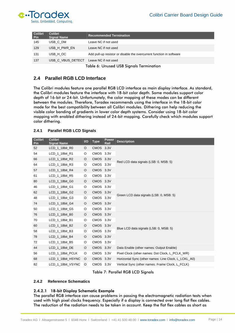
2.4.2.1 18-bit Display Schematic Example
The parallel RGB interface can cause problems in passing the electromagnetic radiation tests when
used with high pixel clocks frequency. Especially if a display is connected over long flat flex cables.
The reduction of the radiation needs to be taken in account. Keep the flat flex cables as short as
Colibri Carrier Board Design Guide
Toradex AG l Altsagenstrasse 5 l 6048 Horw l Switzerland l +41 41 500 48 00 l www.toradex.com l [email protected] Page | 15
possible. Series resistors in the data lines reduce the slew rate of the signals which reduces the
radiation problem but can introduce signal quality and timing problems. The serial resistor value is
a trade-off between electromagnetic radiation reduction and signal quality. A good starting value
is 22Ω.
Figure 6: 18bit Parallel RGB Display Reference Schematic
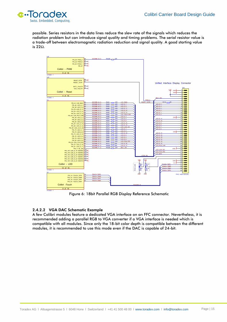
2.4.2.2 VGA DAC Schematic Example
A few Colibri modules feature a dedicated VGA interface on an FFC connector. Nevertheless, it is
recommended adding a parallel RGB to VGA converter if a VGA interface is needed which is
compatible with all modules. Since only the 18-bit color depth is compatible between the different
modules, it is recommended to use this mode even if the DAC is capable of 24-bit.
Colibri Carrier Board Design Guide
Toradex AG l Altsagenstrasse 5 l 6048 Horw l Switzerland l +41 41 500 48 00 l www.toradex.com l [email protected] Page | 16
Figure 7: VGA DAC Reference Schematic
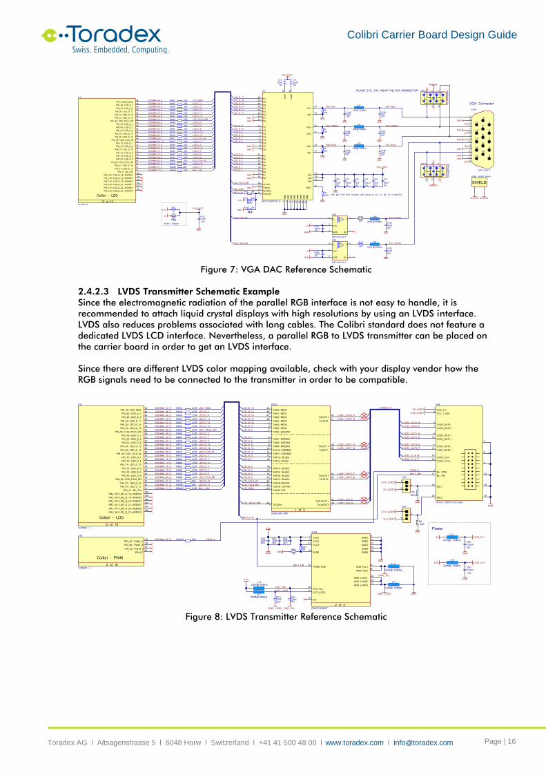
2.4.2.3 LVDS Transmitter Schematic Example
Since the electromagnetic radiation of the parallel RGB interface is not easy to handle, it is
recommended to attach liquid crystal displays with high resolutions by using an LVDS interface.
LVDS also reduces problems associated with long cables. The Colibri standard does not feature a
dedicated LVDS LCD interface. Nevertheless, a parallel RGB to LVDS transmitter can be placed on
the carrier board in order to get an LVDS interface.
Since there are different LVDS color mapping available, check with your display vendor how the
RGB signals need to be connected to the transmitter in order to be compatible.
Figure 8: LVDS Transmitter Reference Schematic

Colibri Carrier Board Design Guide
Toradex AG l Altsagenstrasse 5 l 6048 Horw l Switzerland l +41 41 500 48 00 l www.toradex.com l [email protected] Page | 17
18-bit Color Mapping The color mapping for the 18-bit LVDS interface is standardized and is shown in the following
picture:
Figure 9: 18-bit LVDS Color Mapping
24-bit JEIDA Color Mapping The JEIDA color mapping is compatible with the 18bit LVDS interface. Therefore, the mapping is
sometimes also called “24bit / 18bit Compatible Color Mapping”. The signal names of the color
bits are renamed (e.g. the 18bit R5 is renamed to 24bit R7) but the position of the MSB is kept the
same. The additional least significant bits R0, R1, G0, G1, B0 and B1 are located at the additional
fourth LVDS data pair.
Figure 10: 24-bit JEIDA LVDS Color Mapping
24-bit VESA Color Mapping Most of the 24bit LVDS displays follow the VESA Color mapping. The VESA color mapping does not
rename the signal bits. This means that the position of the MSB is changed since they are available
at the additional data pair. Therefore, the VESA color mapping is not compatible with the 18bit
interface.
Figure 11: 24-bit VESA LVDS Color Mapping
2.4.3 Unused Parallel RGB Interface Signal Termination
All unused parallel RGB interface signals can be left unconnected.
LVDS1_A_CLK+LVDS1_B_CLK+
LVDS1_A_TX0+/-LVDS1_B_TX0+/-
LVDS1_A_TX1+/-LVDS1_B_TX1+/-
LVDS1_A_TX2+/-LVDS1_B_TX2+/-
Previous Cycle Current Cycle Next Cycle
G0 R5 R4 R3 R2 R1 R0
B1 B0 G5 G4 G3 G2 G1
DE VSYNC HSYNC B5 B4 B3 B2
LVDS1_A_CLK+LVDS1_B_CLK+
LVDS1_A_TX0+/-LVDS1_B_TX0+/-
LVDS1_A_TX1+/-LVDS1_B_TX1+/-
LVDS1_A_TX2+/-LVDS1_B_TX2+/-
LVDS1_A_TX3+/-LVDS1_B_TX3+/-
Previous Cycle Current Cycle Next Cycle
G2 R7 R6 R5 R4 R3 R2
B3 B2 G7 G6 G5 G4 G3
DE VSYNC HSYNC B7 B6 B5 B4
N/A B1 B0 G1 G0 R1 R0
LVDS1_A_CLK+LVDS1_B_CLK+
LVDS1_A_TX0+/-LVDS1_B_TX0+/-
LVDS1_A_TX1+/-LVDS1_B_TX1+/-
LVDS1_A_TX2+/-LVDS1_B_TX2+/-
LVDS1_A_TX3+/-LVDS1_B_TX3+/-
Previous Cycle Current Cycle Next Cycle
G0 R5 R4 R3 R2 R1 R0
B1 B0 G5 G4 G3 G2 G1
DE VSYNC HSYNC B5 B4 B3 B2
N/A B7 B6 G7 G6 R7 R6

Colibri Carrier Board Design Guide
Toradex AG l Altsagenstrasse 5 l 6048 Horw l Switzerland l +41 41 500 48 00 l www.toradex.com l [email protected] Page | 18
2.5 HDMI/DVI
The HDMI and DVI interface uses a TMDS compatible physical link to transfer video and optional
audio data. While electrically, HDMI and DVI are both similar, but there can be a few differences in
their protocols. HDMI is the successor of DVI and specifies the additional transport for audio data
and content protection (HDCP). As HDMI is backward compatible, HDMI devices (monitor,
television set etc.) work with DVI signals. Forward compatibility is not guaranteed. Not all DVI
displays accept the HDMI protocol or are HDCP compatible. Please read the datasheet of the
Colibri modules for more information about the provided HDMI and DVI protocols.
The HDMI and DVI interface define different connectors. There are passive adapters available in
both types. Please be advised that both HDMI and HDCP require to be licensed. The HDMI/DVI
signals are available on a dedicated FFC connector. Check carefully to confirm which modules
provide the interface.
2.5.1 HDMI/DVI Signals
Colibri FFC Pin
Colibri Signal Name
I/O Type Power Rail
Description
2 HDMI_1_CLK_P O TDMS HDMI/DVI differential clock positive
3 HDMI_1_CLK_N O TDMS HDMI/DVI differential clock negative
5 HDMI_1_DATA0_P O TDMS HDMI/DVI differential data lane 0 positive
6 HDMI_1_DATA0_N O TDMS HDMI/DVI differential data lane 0 negative
8 HDMI_1_DATA1_P O TDMS HDMI/DVI differential data lane 1 positive
9 HDMI_1_DATA1_N O TDMS HDMI/DVI differential data lane 1 negative
11 HDMI_1_DATA2_P O TDMS HDMI/DVI differential data lane 2 positive
12 HDMI_1_DATA2_N O TDMS HDMI/DVI differential data lane 2 negative
14 HDMI_1_HPD I CMOS 3.3V Hot plug detect
16 HDMI_DDC_SDA I/O OD 3.3V I2C interface for reading the extended display identification data (EDID) over DDC. 15 HDMI_DDC_SCL O OD 3.3V
Table 8: HDMI/DVI Signals
2.5.2 Reference Schematics
2.5.2.1 DVI Schematic Example
There are different configurations of DVI connectors available. The DVI-D (digital) contains only the
native DVI signals The DVI-A (analogue) provides no DVI signals. Only the analogue VGA signals
are provided. The DVI-I (integrated) combines the digital DVI signals and the analogue VGA
signals. For the DVI-A and DVI-I, there are passive adapters available for the D-SUB VGA
connector. There is only one DDC channel available on the DVI-I interface. Therefore, the
connector is not designed to use both links (DVI and VGA) contemporaneously. Nevertheless, there
are Y-cables available which provides a DVI and VGA output contemporaneously. Such cables are
not standardized and provide normally the DDC only on the DVI or VGA output. Please be aware
of the DDC when using such a Y-cable.
The following schematic example shows a DVI-I implementation. It can also be used as an example
for a DVI-D design, just remove the analogue VGA signals. The sync signals for the VGA signals
need to be level shifted from 3.3V to 5V. The same is necessary for the DDC signals. The TDMS
signals need to be ESD protected by using diodes. The schematic example shows a discrete
solution for the level shifting and protection. There are also integrated solutions available.

Colibri Carrier Board Design Guide
Toradex AG l Altsagenstrasse 5 l 6048 Horw l Switzerland l +41 41 500 48 00 l www.toradex.com l [email protected] Page | 19
Figure 12: DVI-I Reference Schematic
2.5.2.2 HDMI Schematic Example
The HDMI connector does not feature an Analogue VGA interface, but there is an optional
Consumer Electronics Control (CEC) interface available on the connector. The location of the CEC
signal is not standardized on the Colibri modules. Check the datasheet of the modules for more
information to the position of the signal. The CEC is a single- wire interface that is used to control
consumer audio and video devices such as television set or AV receivers. There are many different
trade names for CEC (VIERA Link, Anynet+, EasyLink, Aquos Link, BRAVIA Link, etc.). The CEC is a
3.3V interface. Nevertheless, it is recommended to add level shifter from the internal 3.3V logic
level. This eliminates problems with displays that pull-up the signal to other voltage levels.
The I2C signals for the DDC and the hot plug detection (HPD) need to be shifted to/from the 5V
logic level of the HDMI to the Colibri level of 3.3V. The HPD has a 100kΩ pull down resistor
already on the baseboard

Colibri Carrier Board Design Guide
Toradex AG l Altsagenstrasse 5 l 6048 Horw l Switzerland l +41 41 500 48 00 l www.toradex.com l [email protected] Page | 20
Figure 13: HDMI Reference Schematic
2.5.3 Unused HDMI/DVI Signal Termination
All unused HDMI/DVI signals can be left unconnected. The HPD has a 100kΩ pull down resistor on
the module.
Colibri Pin
Colibri Signal Name
Recommended Termination
2 HDMI_1_CLK_P Leave NC if not used
3 HDMI_1_CLK_N Leave NC if not used
5 HDMI_1_DATA0_P Leave NC if not used
6 HDMI_1_DATA0_N Leave NC if not used
8 HDMI_1_DATA1_P Leave NC if not used
9 HDMI_1_DATA1_N Leave NC if not used
11 HDMI_1_DATA2_P Leave NC if not used
12 HDMI_1_DATA2_N Leave NC if not used
14 HDMI_1_HPD Leave NC if not used, 100kΩ resistor on Colibri module
16 HDMI_DDC_SDA Add pull-up resistor or disable the I2C function in software
15 HDMI_DDC_SCL Add pull-up resistor or disable the I2C function in software
Table 9: Unused HDMI/DVI Signals Termination
52435 -2471
1
2
3
4
5
6
7
8
9
10
11
12
13
14
15
16
17
18
19
20
21
22
23
24
X2
GND
GND
GND
GND
GND
GND
GND
TMDS_CLK_P
TMDS_CLK_N
TMDS_DATA0_P
TMDS_DATA0_N
TMDS_DATA1_P
TMDS_DATA1_N
TMDS_DATA2_P
TMDS_DATA2_N
HOTPLUG_DETE CT_T
R1
1K
DDC_SCL_T
DDC_SDA_T
RC LAMP050 4S
1 2 3456D1
1002944 9-111RLF
TDMS_D 2P1
TDMS_D2 _Shield2
TDMS_D2 N3
TDMS_D 1P4
TDMS_D1 _Shield5
TDMS_D1 N6
TDMS_D 0P7
TDMS_D0 _Shield8
TDMS_D0 N9
TDMS_C LKP10
TDMS_C LK_Shield11
TDMS_C LKN12
CEC13
HEC14
DDR_SCL15
DDR_SDA16
GND17
PWR_ 5V_50 mA18
HotPlug_ HECDP19
SH1S1
SH2S2
SH3S3
SH4S4
X1
RC LAMP050 4S
1 2 3456D2
SHIELD SHIELD
SHIELD
TMDS_CLK_P
TMDS_CLK_N
TMDS_DATA0_P
TMDS_DATA0_N
TMDS_DATA1_P
TMDS_DATA1_N
TMDS_DATA2_P
TMDS_DATA2_N
GND
GND
GND
GND
GND
HOTP LUG_DETECT
HDMI_I2C_SCL
HDMI_I2C_SDA
220pF
50V
C1
HOTPLUG_DETECT
HDMI_I2C_SCL
HDMI_I2C_SDA
5V_HDMI
R2
1.8K
R3
1.8K
4.7pF
50V
C2
4.7pF
50V
C3
GND
GND
220R @100MHz
500 mA
L1
220R @100MHz
500 mA
L2
GND
RC LAMP050 4S1 2 3456D3
SHIELD
5V_HDMI
5V_HDMI
DIFF90_50
DIFF90_50
DIFF90_50
DIFF90_50
DIFF90_50
DIFF90_50
DIFF90_50
DIFF90_50
5V
BAT54
D4
5V_HDMI
TMDS_CLK_P
TMDS_CLK_N
TMDS_DATA0_P
TMDS_DATA0_N
TMDS_DATA1_P
TMDS_DATA1_N
TMDS_DATA2_P
TMDS_DATA2_N
FFC Connector

Colibri Carrier Board Design Guide
Toradex AG l Altsagenstrasse 5 l 6048 Horw l Switzerland l +41 41 500 48 00 l www.toradex.com l [email protected] Page | 21
2.6 Analogue VGA
Some Colibri modules feature a dedicated VGA interface on the HDMI FFC connector. For systems
which need to be compatible with a wide range of Colibri modules, it is recommended to use a
parallel RGB to VGA DAC instead of the dedicated VGA interface.
2.6.1 VGA Signals
Colibri FFC Pin
Colibri Signal Name
I/O Type Power Rail
Description
18 VGA_1_R O Analogue Analogue red video (0 to 0.7V)
20 VGA_1_G O Analogue Analogue green video (0 to 0.7V)
22 VGA_1_B O Analogue Analogue blue video (0 to 0.7V)
24 VGA_1_HSYNC O CMOS 3.3V Horizontal sync
23 VGA_1_VSYNC O CMOS 3.3V Vertical sync
16 HDMI_DDC_SDA I/O OD 3.3V/ 5V tolerant I2C interface for reading the extended display identification data
(EDID) over DDC. Signal shared with the HDMI interface 15 HDMI_DDC_SCL O OD
3.3V/ 5V tolerant
Table 10: VGA Signals
2.6.2 Reference Schematics
The horizontal and vertical sync signals need to be level shifted on the baseboard. The DDC signals
on the FFC connector do not require a level shifter since these signals are 5V tolerant. If a different
I2C interface is used as DDC, the shifters are needed. In the VGA connector standard, the carrier
board needs to provide 5V power supply for the EDID memory on the DDC. This allows the system
to read out the EDID information of an attached display even if it is not powered. Unfortunately,
some displays source the 5V internally and also provide internal pull-up resistors to the I2C lines.
This can cause back feeding problems. Therefore we recommend connecting the display and pull-
up resistor 5V supply over a diode to the module supply.
It is mandatory to place on every analogue RGB signal a 150Ω resistor to ground. Place this
resistor as close to the VGA connector as possible. Before this resistor, the signal trace can be
routed with 50Ω impedance. After the resistor, the signal should be routed with 75Ω impedance.
Depending on the layer stack up, 75Ω traces cannot be reached since the trace with is getting too
small. In this case, lower traces impedance (e.g. 50Ω) can be used but the trace length should be
kept short.
All signals on the VGA D-SUB connector need to be ESD protected. TSR diodes can be used. It is
recommended to add a PI-filter to the analogue RGB signals. The values for the capacitors and
inductors depend on the maximum required display resolution. The PI-filter reduces EMI problems,
but also limits the maximum bandwidth of the VGA signal.

Colibri Carrier Board Design Guide
Toradex AG l Altsagenstrasse 5 l 6048 Horw l Switzerland l +41 41 500 48 00 l www.toradex.com l [email protected] Page | 22
Figure 14: VGA Reference Schematic
2.6.3 Unused VGA Interface Signal Termination
All unused VGA interface signals can be left unconnected.
2.7 Parallel Camera Interface
The Colibri module form factor features an 8 bit parallel camera interface as a standard interface.
Depending on the module, there are maybe additional bits available in the type specific area. Only
the 8 bit YUV and ITU-R BT.656 format mode is intent to keep compatible between Colibri
modules. Consult the Colibri datasheets in order to get more information about the additional
available input modes (e. g. Bayer, RGB etc.)
2.7.1 Parallel Camera Signals
Colibri Pin
Colibri Signal Name
I/O Type Power Rail
Description
101 CAM_1_Y0/C0 I CMOS 3.3V
Video input pixel data
103 CAM_1_Y1/C1 I CMOS 3.3V
79 CAM_1_Y2/C2 I CMOS 3.3V
97 CAM_1_Y3/C3 I CMOS 3.3V
67 CAM_1_Y4/C4 I CMOS 3.3V
59 CAM_1_Y5/C5 I CMOS 3.3V
85 CAM_1_Y6/C6 I CMOS 3.3V
65 CAM_1_Y7/C7 I CMOS 3.3V
96 CAM_1_PCLK I CMOS 3.3V Video input pixel clock
81 CAM_1_VSYNC I CMOS 3.3V Video input vertical sync
94 CAM_1_HSYNC I CMOS 3.3V Video input horizontal sync
75 CAM_1_MCLK O CMOS 3.3V Master clock output for the camera. Some Camera might do not need this clock since they use other clock sources
Table 11: Parallel Camera Signals
CRT_VSYNC
CRT_HSYNC
CRT_BLUE
CRT_GREEN
CRT_RED
DDC_CLK
DDC_ DATA
5V
BAT54
D2
VGA_5V
GND
DDC_CLK_T
DDC_DATA_T
CRT_RED_T
CRT_GREEN_T
CRT_BLUE_T
CRT_VSYNC _T
CRT_HSYNC _T
47pF
50V
C12
GND
47pF
50V
C14
GND
10pF
50V
C18
10pF
50VC19150RR9
GND
GND
1.8KR
R19
1.8KR
R17
DDC_CLK
DDC_ DATA
RC
LA
MP
05
04
S
1 2 3456D1
RC
LA
MP
05
04
S1 2 3456
D5
500 mA
220R@100MHz
L1
500 mA
220R@100MHz
L2
500 mA
220R @100MHz
L8
500 mA
220R @100MHzL9
PLACE D1, D3, D4, D5 NEAR THE DVI-I CONNECTOR
SN7 4LVC1G17
NC1
A2
GND3
Y4
VCC5
IC1
SN7 4LVC1G17
NC1
A2
GND3
Y4
VCC5
IC2
5V
5V
GND
33R
R5
33R
R4
C15100nF16V
SHIELD2
600 mA
40R@100MHz
L3
4.7pF
50V
C3 2
4.7p F
50V
C33
VGA_5V VGA_5V
10pF
50V
C20
150RR10
GND
GND10pF
50VC21600 mA
40R@100MHz
L4
10pF
50V
C22
150RR13
GND
GND10pF
50VC23600 mA
40R@100MHz
L5
FH1 2-24S-0.5SV(55)
1
2
3
4
5
6
7
8
9
10
11
12
13
14
15
16
17
18
19
20
21
22
23
24
X6
GND
CRT_VSYNC
CRT_HSYNC
SHIELD2
CRT_BLUE
CRT_GREEN
CRT_RED
GND
GND
GND
FFC Connector
GND GNDVGA_5V
1
1
2
3
4
5
6
7
8
9
2
3
4
5
6
7
8
9
HDR15SN-H
10
11
12
13
14
1510
11
12
13
14
15
X24A
GND
GND
GND
GND
GND
VGA Connector
HDR15SN-H
SHIELD
X24B
SHIELD2 SHIELD2
R305
120R
C13100nF16V
Colibri Carrier Board Design Guide
Toradex AG l Altsagenstrasse 5 l 6048 Horw l Switzerland l +41 41 500 48 00 l www.toradex.com l [email protected] Page | 23
2.7.2 Unused Parallel Camera Interface Signal Termination
All unused parallel camera input signals can be left unconnected if the interface is disabled in
software. It depends on the module whether the signals can be used as GPIO when they are not
used as camera interface.
2.8 SD/MMC/SDIO
The Colibri module form factor features one SD/MMC interfaces as standard interface. The
interface provide up to 4 data bit which can be used for interfacing SD and MMC cards as well as
SDIO interface peripherals. Depending on the module, there might be additional data signals in
order to get an 8bit interface. This bit width is used by MMCplus cards and eMMC memory chips.
The additional data bits are not intent to be compatible between different Colibri modules.
The SD cards know different bus speed modes. The required signal voltage depends on the bus
speed mode. For example the SDR104 mode requires 1.8V signaling. In the Colibri module
definition, all GPIO capable interfaces including the SD/MMC/SDIO are defined for 3.3V. Some
Colibri modules might be capable to switch the voltages of the SD card interface pins to a 1.8V,
but it is not mandatory. Read the according datasheet of the Colibri module.
Even if the bus speed mode requires the signaling voltage of 1.8V, the supply of the card itself is
still 3.3V. Pay attention to the SD card signal pull-up resistors on the carrier board. If the 1.8V
mode should be supported by the carrier board, the voltage for the pull-up resistors also needs to
be switchable. Some Colibri modules might allow removing the pull-up resistors on the carrier
board and using the internal ones only. In this case, this is the preferred solution. Even if the
external pull-up resistors are not mandatory, we recommend adding not assembled pull-up
resistors to the 3.3V rail in order to be compatible with future modules.
Bus Speed Mode Max. Clock Frequency Max. Bus Speed Signal Voltage
Default Speed 25 MHz 12.5 MByte/s 3.3V
High Speed 50 MHz 25 MByte/s 3.3V
SDR12 25 MHz 12.5 MByte/s 1.8V
SDR25 50 MHz 25 MByte/s 1.8V
DDR50 50 MHz 50 MByte/s 1.8V
SDR50 100 MHz 50 MByte/s 1.8V
SDR104 208 MHz 104 MByte/s 1.8V
Table 12: SD Card Bus Speed Modes
2.8.1 SD/MMC/SDIO Signals
Colibri Pin
Colibri Signal Name
I/O Type Power Rail
Description
192 SD_1_DATA0 I/O CMOS 3.3V
Data signals [3:0], used for SD, MMC and SDIO interfaces, add external pull-up resistors
49 SD_1_DATA1 I/O CMOS 3.3V
51 SD_1_DATA2 I/O CMOS 3.3V
53 SD_1_DATA3 I/O CMOS 3.3V
190 SD_1_CMD I/O CMOS 3.3V Command signal, add external pull-up resistor
47 SD_1_CLK O CMOS 3.3V Clock output
Table 13: 4bit SD/MMC/SDIO Signals
Colibri Carrier Board Design Guide
Toradex AG l Altsagenstrasse 5 l 6048 Horw l Switzerland l +41 41 500 48 00 l www.toradex.com l [email protected] Page | 24
2.8.2 Reference Schematics
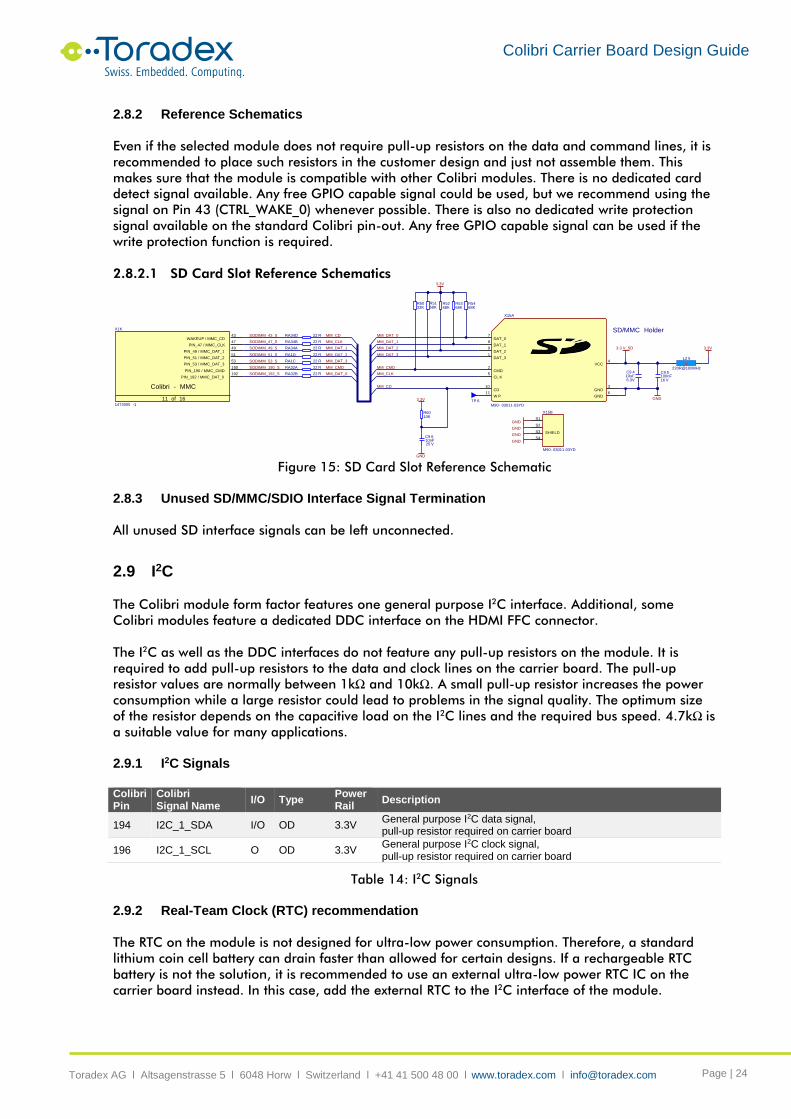
Even if the selected module does not require pull-up resistors on the data and command lines, it is
recommended to place such resistors in the customer design and just not assemble them. This
makes sure that the module is compatible with other Colibri modules. There is no dedicated card
detect signal available. Any free GPIO capable signal could be used, but we recommend using the
signal on Pin 43 (CTRL_WAKE_0) whenever possible. There is also no dedicated write protection
signal available on the standard Colibri pin-out. Any free GPIO capable signal can be used if the
write protection function is required.
2.8.2.1 SD Card Slot Reference Schematics
Figure 15: SD Card Slot Reference Schematic
2.8.3 Unused SD/MMC/SDIO Interface Signal Termination
All unused SD interface signals can be left unconnected.
2.9 I2C
The Colibri module form factor features one general purpose I2C interface. Additional, some
Colibri modules feature a dedicated DDC interface on the HDMI FFC connector.
The I2C as well as the DDC interfaces do not feature any pull-up resistors on the module. It is
required to add pull-up resistors to the data and clock lines on the carrier board. The pull-up
resistor values are normally between 1kΩ and 10kΩ. A small pull-up resistor increases the power
consumption while a large resistor could lead to problems in the signal quality. The optimum size
of the resistor depends on the capacitive load on the I2C lines and the required bus speed. 4.7kΩ is
a suitable value for many applications.
2.9.1 I2C Signals
Colibri Pin
Colibri Signal Name
I/O Type Power Rail
Description
194 I2C_1_SDA I/O OD 3.3V General purpose I2C data signal, pull-up resistor required on carrier board
196 I2C_1_SCL O OD 3.3V General purpose I2C clock signal, pull-up resistor required on carrier board
Table 14: I2C Signals
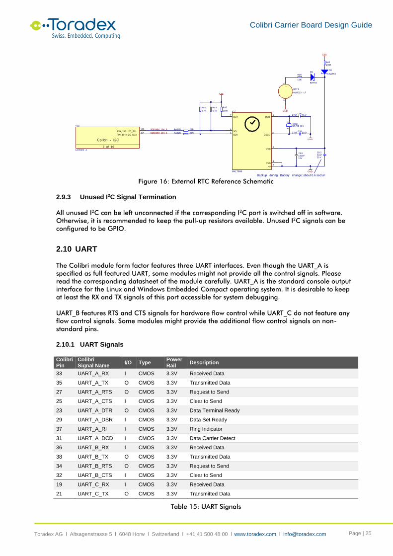
2.9.2 Real-Team Clock (RTC) recommendation
The RTC on the module is not designed for ultra-low power consumption. Therefore, a standard
lithium coin cell battery can drain faster than allowed for certain designs. If a rechargeable RTC
battery is not the solution, it is recommended to use an external ultra-low power RTC IC on the
carrier board instead. In this case, add the external RTC to the I2C interface of the module.
MM_CD
100nF16 V
C9 510uF6.3V
C9 4
3.3V
GND
2A220R@100MHz
L2 5
R5033K
3.3V
1473005 -1
PIN_47 / MMC_CLK47
PIN_49 / MMC_DAT_149
PIN_51 / MMC_DAT_251
PIN_53 / MMC_DAT_353
PIN_190 / MMC_CMD190
PIN_192 / MMC_DAT_0192
WAKEUP / MMC_CD43
Colibri - MMC
11 of 16
X1K
SODIMM_47_S
SODIMM_49_S
SODIMM_51_S
SODIMM_53_S
SODIMM_43_S
SODIMM_190_S
SODIMM_192_S
3.3 V_SD
10nF25 V
C9 6
3.3V
GND
22 RRA1C
22 RRA1D
22 RRA32A
22 RRA32B
22 RRA34B
22 RRA34A
22 RRA34D MM_DAT_0
MM_DAT_1
MM_DAT_2
MM_DAT_3
MM_CMD
MM_CLK
TP 6M90- 03011-03YD
DAT_31
CMD2
VCC4
CL K5
GND6
DAT_07
DAT_18
CD10
DAT_29
GND3
W P11
X15A
SD/MMC HolderMM_CD
MM_DAT_0
MM_DAT_1
MM_DAT_2
MM_DAT_3
MM_CMD
MM_CLK
GND
GND
GND
GND
M90- 03011-03YD
SHIELD
S1
S2
S3
S4
X15B
R5168K
R5268K
R5368K
R5468K
R6010K
Colibri Carrier Board Design Guide
Toradex AG l Altsagenstrasse 5 l 6048 Horw l Switzerland l +41 41 500 48 00 l www.toradex.com l [email protected] Page | 25
Figure 16: External RTC Reference Schematic
2.9.3 Unused I2C Signal Termination
All unused I2C can be left unconnected if the corresponding I
2C port is switched off in software.
Otherwise, it is recommended to keep the pull-up resistors available. Unused I2C signals can be
configured to be GPIO.
2.10 UART
The Colibri module form factor features three UART interfaces. Even though the UART_A is
specified as full featured UART, some modules might not provide all the control signals. Please
read the corresponding datasheet of the module carefully. UART_A is the standard console output
interface for the Linux and Windows Embedded Compact operating system. It is desirable to keep
at least the RX and TX signals of this port accessible for system debugging.
UART_B features RTS and CTS signals for hardware flow control while UART_C do not feature any
flow control signals. Some modules might provide the additional flow control signals on non-
standard pins.
2.10.1 UART Signals
Colibri Pin
Colibri Signal Name
I/O Type Power Rail
Description
33 UART_A_RX I CMOS 3.3V Received Data
35 UART_A_TX O CMOS 3.3V Transmitted Data
27 UART_A_RTS O CMOS 3.3V Request to Send
25 UART_A_CTS I CMOS 3.3V Clear to Send
23 UART_A_DTR O CMOS 3.3V Data Terminal Ready
29 UART_A_DSR I CMOS 3.3V Data Set Ready
37 UART_A_RI I CMOS 3.3V Ring Indicator
31 UART_A_DCD I CMOS 3.3V Data Carrier Detect
36 UART_B_RX I CMOS 3.3V Received Data
38 UART_B_TX O CMOS 3.3V Transmitted Data
34 UART_B_RTS O CMOS 3.3V Request to Send
32 UART_B_CTS I CMOS 3.3V Clear to Send
19 UART_C_RX I CMOS 3.3V Received Data
21 UART_C_TX O CMOS 3.3V Transmitted Data
Table 15: UART Signals
GND
100nF16V
C93
M41T0M6
OSCI1
OSCO2
VCC
VSS4
NF3
OUT7
SCL6
SDA5
IC7
R47
100K
3.3V
R45
4.7K
R4 6
4.7K
32.768 KHz
12
OSC1
BAT54
D8
3.3V
GND
22uF25 V
C9 21473005 -1
PIN_194 / I2C_SDA194
PIN_196 / I2C_SCL196
Colibri - I2C
7 of 16
X1G
GND
10R
R49
BAT54
D9
SODIMM_194_S
SODIMM_196_S
HU2032- LF
+1
-2
BAT1
470R
R48
22RRA32C
22RRA32D
Backup during Battery change: about 0.6 sec/uF
27pF 50 VC91
27pF 50 VC90
8
Colibri Carrier Board Design Guide
Toradex AG l Altsagenstrasse 5 l 6048 Horw l Switzerland l +41 41 500 48 00 l www.toradex.com l [email protected] Page | 26
2.10.2 Reference Schematics
2.10.2.1 Full Featured RS232 Reference Schematics
The RS232 interface can be classified as Data Terminal Equipment (DTE) or Data Communication
Equipment (DCE). This classification is inherited from the usage of the interface for modems. The
signal direction of these modes is different. Some Colibri modules might allow changing the mode,
and therefore, also the data direction, but this is not a mandatory requirement. According to the
Colibri specifications, the interface is intent to be used in the DTE configuration.
Signal Name Usage DTE Direction (Colibri standard)
DCE Direction
UART_A_RXD Received Data Data from DCE to DTE Input Output
UART_A_TXD Transmitted Data Data from DTE to DCE Output Input
UART_A_RTS Request to Send DTE request to DCE to be prepared to receive data
Output Input
UART_A_CTS Clear to Send DCE indicates ready to accept data Input Output
UART_A_DTR Data Terminal Ready DTE indicates presence to DCE Output Input
UART_A_DSR Data Set Ready DCE is ready to receive commands or data Input Output
UART_A_RI Ring Indicator DCE announce to have detected an incoming ring signal on the telephone line
Input Output
UART_A_DCD Data Carrier Detect DCE announce to be connected to the telephone line
Input Output
Table 16: RS232 Signal Modes
Figure 17: RS232 Reference Schematic
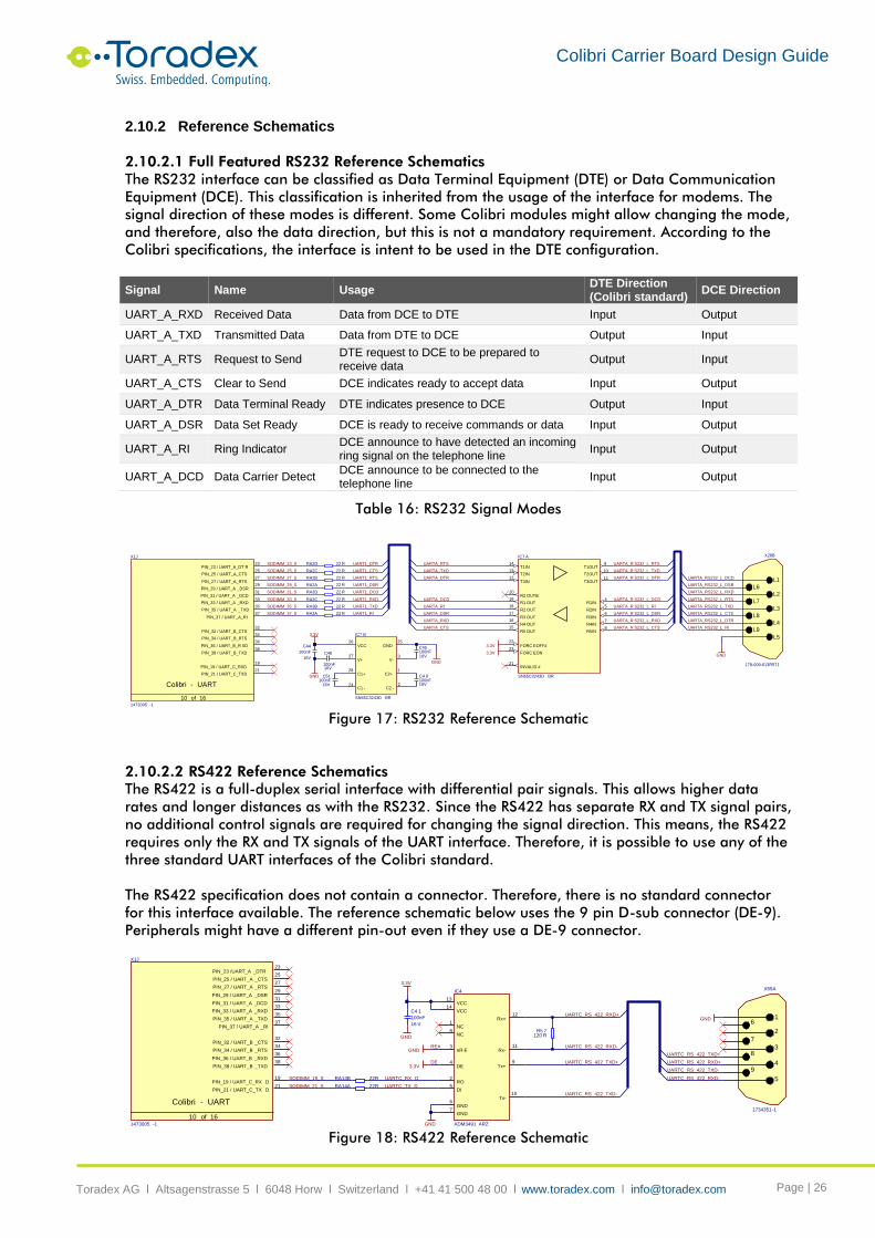
2.10.2.2 RS422 Reference Schematics
The RS422 is a full-duplex serial interface with differential pair signals. This allows higher data
rates and longer distances as with the RS232. Since the RS422 has separate RX and TX signal pairs,
no additional control signals are required for changing the signal direction. This means, the RS422
requires only the RX and TX signals of the UART interface. Therefore, it is possible to use any of the
three standard UART interfaces of the Colibri standard.
The RS422 specification does not contain a connector. Therefore, there is no standard connector
for this interface available. The reference schematic below uses the 9 pin D-sub connector (DE-9).
Peripherals might have a different pin-out even if they use a DE-9 connector.
Figure 18: RS422 Reference Schematic
SN65C3243D BR
T3IN12
T2IN13
T1IN14
R2 OUTB20
R1 OUT19
R2 OUT18
R3 OUT17
R4 OUT16
R5 OUT15
FORC EOFF#22
FORC EON23
INVALID #21
T1OUT9
T2OUT10
T3OUT11
R1IN4
R2IN5
R3IN6
R4IN7
R5IN8
IC7 A
178-009-613R571
L1
L2
L3
L4
L5
L6
L7
L8
L9
X28B
GND
UARTA_R S232_L_RTS
UARTA_R S232_L_TXD
UARTA_R S232_L_DTR
UARTA_R S232_L_DCD
UARTA_R S232_L_RI
UARTA_R S232_L_DSR
UARTA_R S232_L_RXD
UARTA_R S232_L_CTS
UARTA_RS232_L_RTS
UARTA_RS232_L_TXD
UARTA_RS232_L_DTR
UARTA_RS232_L_DCD
UARTA_RS232_L_RI
UARTA_RS232_L_DSR
UARTA_RS232_L_RXD
UARTA_RS232_L_CTS
UARTA_CTS
UARTA_DSR
UARTA_RI
UARTA_DCD
UARTA_DTR
UARTA_TXD
UARTA_RTS
3.3V
3.3V
UARTA_RXD
SN65C3243D BR
VCC26
V+27
C1+28
C1 -24
GND25
V-
C2+1
C2 -
IC7 B
GND
GND100nF16V
C48
C44
100nF
16V
100nF16V
C51
100nF16V
C45
100nF16V
C4 9
3.3V
UART1_CTS
UART1_DSR
UART1_RI
UART1_DCD
UART1_DTR
UART1_TXD
UART1_RTS
UART1_RXD
1473005 -1
PIN_19 / UART_C_RXD19
PIN_21 / UART_C_TXD21
PIN_23 / UART_A_DT R23
PIN_25 / UART_A_CTS25
PIN_27 / UART_A_RTS27
PIN_29 / UART_A _DSR29
PIN_31 / UART_A _DCD31
PIN_33 / UART_A _RXD33
PIN_35 / UART_A _TXD35
PIN_37 / UART_A_RI37
PIN_32 / UART_B_CTS32
PIN_34 / UART_B_RTS34
PIN_36 / UART_B_R XD36
PIN_38 / UART_B_TXD38
Colibri - UART
10 of 16
X1J
SODIMM_23_S
SODIMM_25_S
SODIMM_27_S
SODIMM_29_S
SODIMM_31_S
SODIMM_33_S
SODIMM_35_S
SODIMM_37_S
22 RRA2A
22 RRA2B
22 RRA2C
22 RRA2D
22 RRA3A
22 RRA3B
22 RRA3C
22 RRA3D
3
2
ADM3491 ARZ
Rx+12
Rx-11
Tx-10
Tx+9
NC1
RO2
nR E3
DE4
DI5
GND6
GND7
NC8
VCC13
VCC14
IC4
DE
RE#
100nF
16 V
C4 1
GND
UARTC_RS 422_TXD+
UARTC_RS 422_TXD-
UARTC_RS 422_RXD-
UARTC_RS 422_RXD+
GND
UARTC_RS 422_RXD-
UARTC_RS 422_RXD+
UARTC_RS 422_TXD+
UARTC_RS 422_TXD-
R5 7120 R
1
2
3
4
5
6
7
8
9
1734351-1
X55A
3.3V
22RRA14A
22RRA14B
3.3V
GND
UARTC_RX D
UARTC_TX D
GND1473005 -1
PIN_19 / UART_C_RX D19
PIN_21 / UART_C_TX D21
PIN_23 /UART_A _DTR23
PIN_25 / UART_A _CTS25
PIN_27 / UART_A _RTS27
PIN_29 / UART_A _DSR29
PIN_31 / UART_A _DCD31
PIN_33 / UART_A _RXD33
PIN_35 / UART_A _TXD35
PIN_37 / UART_A _RI37
PIN_32 / UART_B _CTS32
PIN_34 / UART_B _RTS34
PIN_36 / UART_B _RXD36
PIN_38 / UART_B _TXD38
Colibri - UART
10 of 16
X1J
SODIMM_19_S
SODIMM_21_S

Colibri Carrier Board Design Guide
Toradex AG l Altsagenstrasse 5 l 6048 Horw l Switzerland l +41 41 500 48 00 l www.toradex.com l [email protected] Page | 27
2.10.2.3 RS485 Reference Schematics
The RS485 interface is a half-duplex serial interface with differential pair signals. Instead of two
differential pair wires (RS422), only one pair is used for transmitting and receiving the data. The
bus allows multi point connections. Since the transceiver needs to be set either in the transmitting
or receiving mode, an additional control signal is required. It is recommended to use the RTS signal
of the corresponding UART interface. The RTS signal is only available on the UART_A and UART_B
as Colibri standard interface. The schematic below inverts the RTS signal for the data enable input
of the transceiver. Some modules allow inverting the signal in software, but it is recommended to
use the inverter circuit shown below in order to maintain compatibility with different modules and
drivers provided by Toradex. For some applications, it is desirable that the UART controller does
not see the TX message on its RX pins (echo of the sent message). In this case, the receive enable
pin (RE#) can be driven as well with the RTS signal. This turns off the RX output buffer while
sending a message.
Like the RS422, the RS485 specification also does not describe a standard connector. The reference
schematic below uses a DE-9 connector which may have a different pin-out as some peripheral
devices.
Figure 19: RS485 Reference Schematic
2.10.2.4 IrDA Reference Schematics
IrDA is an optical wireless communication interface. There are different physical layer modulation
schemes available. Make sure which modes are supported by the specific Colibri module and the
peripheral devices. For compatibility reasons, it is recommended to use UART_C for the IrDA
implementation. Some modules only feature the IrDA function on this UART instance.
Figure 20: IrDA Reference Schematic
2.10.3 Unused UART Signal Termination
Unused UART interface signals can be left unconnected. For debugging purpose, it is
recommended to have at least the UART1_RXD and UART1_TXD signals available.
DE
RE#
GND
100nF
16 V
C41
GND UARTB _RS485_D+
UARTB _RS485_D-
GND
R57120R
1
2
3
4
5
6
7
8
9
1734351-1
X55A3.3V
UARTB _TXD
UARTB _RXD
680 RR58
680 RR60
GND
3.3V
ADM3491ARZ
Rx+12
Rx-11
Tx-
Tx+9
NC1
RO2
nRE3
DE4
DI5
GND6
GND7
NC8
VCC13
VCC14
IC4
NC1
A
2
GND3
Y
VCC5
IC2
SN74 LVC1 G04DC KR
3.3V
GND
0R
R20
R2 1
100 K
22RR1 0
22RR11
22RR1 2
GND
Assemble R20 and remove R21
not get an echo of the sent message )
ECHO disabled (the sender does1473005 -1
PIN_19 / UART_C_RXD19
PIN_21 / UART_C_TXD21
PIN_23 / UART_A_DTR23
PIN_25 / U ART_A_CTS25
PIN_27 / UART_A _RTS27
PIN_29 / UART_A _DSR29
PIN_31 / UART_A _DCD31
PIN_33 / UART_A _RXD33
PIN_35 / UART_A _TXD35
PIN_37 / UART_A _RI37
PIN_32 / UART_B _CTS32
PIN_34 / UART_B _RTS34
PIN_36 / UART_B _RXD36
PIN_38 / UART_B _TXD38
Colibri - UART
10 of 16
X1J
NA
NA
NA
4
10
22RR10
22RR11
TFDU4101
1
2
3
4
5
6
7
8
X30
22RR6 6
0RR67
4.7uF10V
+C62100n F16V
C57
GNDR6 9
100KGND
UARTC_IRDA_SD
R6 8
4.7R
IrDA Transceiver
3.3V_SW
3.3V_SWUARTC_IRDA_LED
UARTC_IRDA_VCC
UARTC_RXD
UARTC_TXD
147300 5-1
PIN_19 / UART_C_RXD19
PIN_21 / UART_C_TXD21
PIN_23 / UART_A_DTR23
PIN_25 / UART_A_CTS25
PIN_27 / UART_A_RTS27
PIN_29 / UART_A_DSR29
PIN_31 / UART_A_DCD31
PIN_33 / UART_A_RXD33
PIN_35 / UART_A_TXD35
PIN_37 / UART_A_RI37
PIN_32 / UART_B_CTS32
PIN_34 / UART_B_RTS34
PIN_36 / UART_B_RXD36
PIN_38 / UART_B_TXD38
Colibri - UART
10 of 16
X1J
LED_K
TXD
RXD
SD
VCC
NC
GND
LED_A

Colibri Carrier Board Design Guide
Toradex AG l Altsagenstrasse 5 l 6048 Horw l Switzerland l +41 41 500 48 00 l www.toradex.com l [email protected] Page | 28
2.11 SPI
The serial peripheral interface (SPI) bus is a synchronous, full duplex interface. The Colibri module
form factor features one SPI interface. The interface has a chip select signal as compatible
standard. Some module may feature additional chip select signal or additional SPI interfaces as
secondary function of other pins.
The clock polarity and phase of the SPI bus is not standardized. Some peripherals are latching the
data on the positive edge of the clock while others are latching it at the negative edge. The SPI
modes describe these different behaviors. Make sure that the according Colibri module and the
peripheral device can be set to the same SPI mode.
SPI Mode Clock Polarity
Clock Phase
Description
0 0 0 Clock is positive polarity and the data is latched on the positive edge of SCK
1 0 1 Clock is positive polarity and the data is latched on the negative edge of SCK
2 1 0 Clock is negative polarity and the data is latched on the positive edge of SCK
4 1 1 Clock is negative polarity and the data is latched on the negative edge of SCK
Table 17: SPI Modes
2.11.1 SPI Signals
The SPI bus consists of one master and one or many slaves. In the Colibri standard, the module is
the SPI master. Some modules might allow to be used also as SPI slaves. Some modules may
provide this function on different, non-standard pins.
Colibri Pin
Colibri Signal Name
I/O Type Power Rail
Description
92 SPI_1_MOSI O CMOS 3.3V Master Output, Slave Input
90 SPI_1_MISO I CMOS 3.3V Master Input, Slave Output
86 SPI_1_CS0 O CMOS 3.3V Slave Select
88 SPI_1_CLK O CMOS 3.3V Serial Clock
Table 18: SPI Signals
2.11.2 Unused SPI Signal Termination
Unused SPI signals can be left unconnected.
2.12 CAN
The Colibri form factor does not provide a controller area network (CAN) bus as a standard
interface. Some modules feature dedicated CAN interface signals. For the other modules, it is
recommended to add an SPI to CAN controller on the carrier board for providing a CAN interface.
This section describes how to add a CAN controller to the SPI interface. If you intent to use the
dedicated CAN interface signals, please read the datasheet of the Colibri module.
2.12.1 Reference Schematics
Besides a controller, the CAN interface requires a transceiver on the carrier board. Normally, the
CAN interface needs to be galvanically isolated from the Colibri computer module. There are
transceivers with integrated signal isolation coupler and isolated DC/DC converters available (for
example the Analog Devices ADM3053). The other solution is to use separate components for the
transceiver, signal coupler and DC/DC converter. There are different type of connectors used for
the CAN interface. The reference schematic below uses a DE-9 connector. Since this is not an
official standard, some devices might have a different pin-out.

Colibri Carrier Board Design Guide
Toradex AG l Altsagenstrasse 5 l 6048 Horw l Switzerland l +41 41 500 48 00 l www.toradex.com l [email protected] Page | 29
Figure 21: CAN Reference Schematic
2.13 PWM
The Colibri module form factor defines four general purpose pulse width modulator (PWM)
outputs. Please note that two of the four PWM signals are located on pins that are also used for the
standard parallel camera interface. These PWM outputs can only be used if the according camera
pins are not in use. The maximum output frequency and the available duty cycle steps can also
vary between the different Colibri modules.
2.13.1 PWM Signals
Colibri Pin
Colibri Signal Name
I/O Type Power Rail
Description
59 PWM_A O CMOS 3.3V General purpose PWM output, pin also used for camera interface
28 PWM_B O CMOS 3.3V General purpose PWM output
30 PWM_C O CMOS 3.3V General purpose PWM output
67 PWM_D O CMOS 3.3V General purpose PWM output, pin also used for camera interface
Table 19: PWM Signals
2.13.2 Reference Schematics
The PWM output signals can be used for example to drive, motors, LEDs, robotic servos or fans. It is
possible to get an analogue signal with a simple low-pass filter. A very common usage is driving of
the backlight of liquid crystal displays.
Figure 22: PWM Example Schematic
2.13.3 Unused PWM Signal Termination
Unused PWM signals can be left unconnected.
1473005 -1
PIN_86 / SSPFRM86
PIN_88 / SSPSCLK88
PIN_90 / SSPRXD90
PIN_92 / SSPTXD92
Colibri - SSP/CAN
6 of 16
PIN_73 / CAN_INT#73
X1F
SODIMM_86
SODIMM_88
SODIMM_90
SODIMM_92
SODIMM_73
MCP2515 T-I/ST
TX CAN1
RXCAN2
CL KOUT/SOF 3
nTX0RTS4
nTX1RTS5
NC6
nTX2RTS7
OSC28
OSC19
VSS10
VDD20
nRESET19
nCS18
SO17
SI16
NC15
SCK14
nINT13
nRX0BF12
nRX1BF11
IC18
SSP_SCLK
SSP_FRM
SSP_TXD
SSP_RXD
CAN_INT#
100nF
16VC159GND
3.3V
GND
16.0 MHz
1 2
OSC3
22pF
50V
C163
22pF
50V
C162
GND GND
RESET_OUT #
22 RRA11A
22 RRA11B
22 RRA9C
22 RRA9D
22 RRA30C
CAN_TX
CAN_RX
100nF16V
C105100nF16V
C106
CAN_L
CAN_H
CAN_ GND_I SOGND
CAN_5 V_ISO
0R
R10 6
3.3V
CAN_GND_I SO
5V
ADM3053BRWZ
VCC8
VIO6
VISOOUT12
VISOIN19
VREF14
RXD4
TX D5
CANL15
CANH17
RS18
GND1_23
GND1_39
GND1_47
GND1_510
GND1_11
GND2_211
GND2_316
GND2_413
GND2_120
NC2
CAN
IC10
10uF10V
C10410uF10V
C107
100nF16V
C109
GND
10nF25V
C108100nF16 V
C11110nF25V
C110
CAN_5 V_ISO
CAN_ GND_I SO
56RR107
56RR108
47nF
16 VC112
CAN_ GND_I SO
CAN_PGND
R99
100 R
CAN_PW
U1
U2
U3
U4
U5
U6
U7
U8
U9
178- 009- 613R571
X32A
CAN Connector
CAN_5 V_ISO
CAN_ GND_I SO
0R
R100
0R
R101
NA
NA
GREEN
LED16
RED
LED17
R90
120R
R91
120R
3.3V 3.3V
SSP_SCLK
SSP_FRM
SSP_TXD
SSP_RXD
CAN_INT#
1473005 -1
VDD_ FAULT#
BATT_ FAULT# 24
RESET_EXT#26
RESET_OUT #
Colibri - Reset
4 of 16
X1D
87
22
1473005 -1
PIN_59 / PW M_A 59
PIN_67
PIN_28 / PW M_B 28
PIN_30 / PW M_C30
Colibri - PWM
5 of 16
X1E
SODIMM_59
SODIMM_28
SODIMM_30
SODIMM_67
R98 10K
R99 10K
330nF16 V
C155
GND GND
22RRA33A
22RRA29D
3
5
4
SI-1024-X
T5B
2
16
SI-1024-X
T5A
GREEN
LED3
R124
120 R
3.3V
GND
R128
100 K
3.3 V
GNDGND
GND
GREEN
LED4
120 R
R131
100 K
1
2
3
X2
GND
PWM_A
PWM_B
PWM_C
PWM_D
330nF16 V
C154
67
Colibri Carrier Board Design Guide
Toradex AG l Altsagenstrasse 5 l 6048 Horw l Switzerland l +41 41 500 48 00 l www.toradex.com l [email protected] Page | 30
2.14 Analogue Audio
2.14.1 Analogue Audio Signals
If only single channel (mono) line input or headphone output is required, it is recommended to use
the left channel.
Colibri Pin
Colibri Signal Name
I/O Type Power Rail
Description
1 ANALOG_AUDIO_MIC_IN I Analogue 3.3V Microphone input
3 ANALOG_AUDIO_MIC_GND Analogue Microphone pseudo-ground
5 ANALOG_AUDIO_LINEIN_L I Analogue 3.3V Left line input
7 ANALOG_AUDIO_LINEIN_R I Analogue 3.3V Right line input
15 ANALOG_AUDIO_HEADPHONE_L O Analogue 3.3V Headphone left output (can also be used as line left output)
17 ANALOG_AUDIO_HEADPHONE_R O Analogue 3.3V Headphone right output (can also be used as line right output)
13 ANALOG_AUDIO_HEADPHONE_GND Analogue Headphone pseudo-ground (do not connect to ground!)
Table 20: Analogue Audio Signals
2.14.2 Reference Schematics
Depending on the module, the headphone output signals can have a DC offset. A common
solution is adding series capacitors to the headphone signal lines. If the headphone output signals
are used only as line output signals, 1µF series capacitors are sufficient. If the signals are used for
driving headphones, larger capacitors (47µF and more) are recommended. Some Colibri modules
provide a virtual headphone ground that can be used instead of the series capacitors in order to
reduce the BOM cost. Please note this solution only works if the attached device is isolated from
the module ground. For example, this works perfectly for headphones, but does not work for an
audio amplifier that uses the same ground as the module.
The line-in and microphone signals do not require serial capacitors since they are already placed
on the module. Some microphones (e.g. the widely used electret microphones) require a phantom
power. The reference schematic below shows a suitable solution for common electret microphone
capsules. Please note that some microphones require providing the phantom power on the middle
ring of the 3.5mm jack while others need to be powered over the tip of the 3.5mm jack which is
also used for the audio signals. The Colibri modules features a special analog ground for the
microphone. This is basically a switched ground. Using this ground instead of the regular analog
ground allows switching off the phantom power when the microphone is not in use.

Colibri Carrier Board Design Guide
Toradex AG l Altsagenstrasse 5 l 6048 Horw l Switzerland l +41 41 500 48 00 l www.toradex.com l [email protected] Page | 31
Figure 23: Analogue Audio Reference Schematic
Figure 24: Analogue Audio Reference Schematic (using virtual and switched grounds)
2.14.3 Unused Analogue Audio Signal Termination
The unused analogue audio signals can be left unconnected. Please note, even if the analogue
audio interface is not used at all, the analogue 3.3V power pins of the module (pin 10 and 12) still
needs to be powered. Alternatively, the analogue power can be connected to the digital 3.3V
power rail.
47uF6.3V+C4
47uF6.3V+C5
15pF50V
C115pF50V
C2
GND
GND
LINEIN_L
LINEIN_R
HEADPHONE_L
HEADPHONE_R
AUDIO[0..6]
AUDIO_AGND
147300 5-1
PIN_1 / MIC_IN1
PIN_5 / LINEIN_L5
PIN_7 / LINEIN_R_7
PIN_13 / HEADPHONE_GND13
PIN_15 / HEADPHONE_L15
PIN_1 7 / HEADPHONE_R17
PIN_3 / MIC_GND3
Colibri -Audio
8 of 16
X1H
MIC_IN
MIC_GND
LINEIN_R
LINEIN_L
HEADPHONE_GND
HEADPHONE_L
HEADPHONE_R
PJ3X01RF0 4B-H
1
25
22
24
23
HEADP. OUT - Green
2 of 3
X26B
PJ3X01RF0 4B-H
1
35
32
34
33
LINE IN - Blue
3 of 3
X26C
PJ3X01RF0 4B-H
1
5
2
4
3
MIC IN - Pink
2 of 3
X26A
MIC_I N
R2
100R
47uF6.3V
+C10
AUDIO _AVCC
R1
2.2K
R3
2.2K
GND
MIC_G ND
HEADPHONE_GND
TP1
TP2
HEADPHONE_AC_L
HEADPHONE_AC_R
Place close toMicrophone Connector
Top Jack
Middle Jack
Bottom Jack
3.3V2.2uF6.3V
C8 9
GND
5V
2.2uF6.3V
C8 8
AUD IO_AGND
2A
220R @100MHz
L24
GND
AUD IO_AVCC
Vin1
GND2
N/C4
Vout
E3
NC P511SN33T 1G
IC6
Audio VCC Circuit
GND
AUD IO_ AVCC
147300 5-1
GND39
GND41
GND83
GND109
GND147
GND181
GND197
GND199
VCC_BATT40
3V342
3V3108
3V3182
3V3198
3V3200
3V384
3V3148
PIN_9 / VSS_AUDIO9
PIN_11 / VSS_AUDIO11
Colibri - Power Supply
1 of 16
VDD _ANALOG10
VDD _ANALOG12
X1A
AUD IO_AGND
3.3V
SHIELD
JA3333L -D11P-4F
S1
S2
S3
S4
SHIELD
X26D
SHIELD
SHIELD
SHIELD
15pF 50V
C11
15pF50V
15pF 50V
C8
50V15pF
C8
C615pF50V
C7
15pF50V
C9
5
AUDIO_AGND
AUDIO_AGND
15pF
50V
C6
15pF
50V
C7
AUD IO_AGND
15pF
50V
C1
15pF
50V
C2
GND
GND
LINEIN_L
LINEIN_R
HEADPHONE_L
HEADPHONE_R
AUDIO[0..6]
15pF
50V
C9
147300 5-1
PIN_1 / MIC_IN1
PIN_5 / LINEIN_L5
PIN_7 / LINEIN_R7
PIN_13 / HEADPHONE_GND13
PIN_15 / HEADPHONE_L15
PIN_17 / HEADPHONE_R17
PIN_3 / MIC_GND3
Colibri -Audio
8 of 16
X1H
MIC_IN
MIC_GND
LINEIN_R
LINEIN_L
HEADPHONE_GND_
HEADPHONE_L
HEADPHONE_R
PJ3X01RF0 4B-H
1
25
22
24
23
HEADP. OUT - Green
2 of 3
X26B
PJ3X01RF0 4B-H
1
35
32
34
33
LINE IN - Blue
3 of 3
X26C
PJ3X01RF0 4B-H
1
5
2
4
3
MIC IN - Pink
2 of 3
X26A
MIC_IN
R2100R
47uF6.3V
+C10
AUD IO_AVCC R1 2.2K
R3 2.2K
GND
MIC_GND
HEADPHONE_GND
Place close to
Microphone Connector
Top Jack
Middle Jack
Bottom Jack
3.3V2.2uF6.3V
C8 9
GND
5V
2.2uF6.3V
C88
AUD IO_AGND
2A
220R @100MHz
L24
GND
AUDIO_AVCC
Vin1
GND2
N/C4
Vout
E3
NC P511SN33T 1G
IC6
Audio VCC Circuit
GND
AUDIO_AVCC
147300 5-1
GND39
GND41
GND83
GND109
GND147
GND181
GND197
GND199
VCC _BATT40
3V342
3V3108
3V3182
3V3198
3V3200
3V384
3V3148
PIN_9 / VSS_AUD IO9
PIN_11 / VSS_AUD IO11
Colibri - Power Supply
1 of 16
VDD _ANALOG10
VDD _ANALOG12
X1A
AUDIO_AGND
3.3V
Virtual ground (voltag e offset)
Do not connect to normal ground!
Switched groundSHIELD
JA3333L -D11P-4F
S1
S2
S3
S4
SHIELD
X26D
SHIELD
SHIELD
SHIELD
C11
C3
15pF
50V
15pF
50V
C8
15pF
50V
5
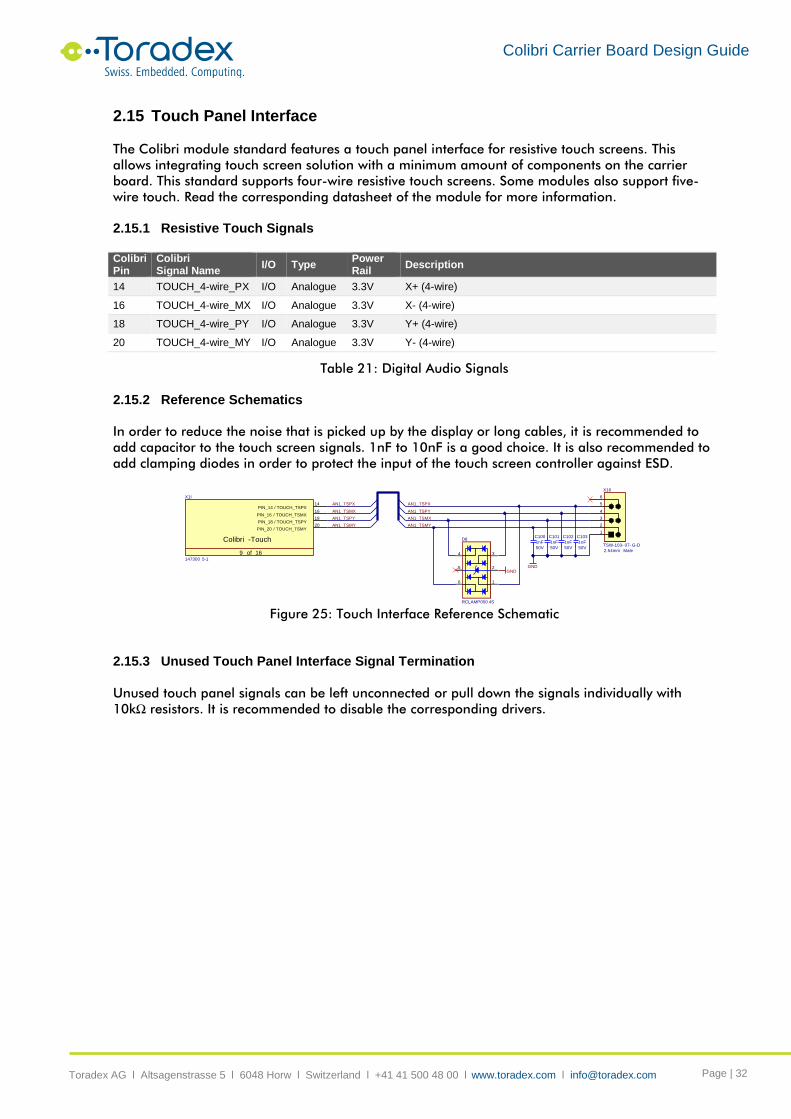
Colibri Carrier Board Design Guide
Toradex AG l Altsagenstrasse 5 l 6048 Horw l Switzerland l +41 41 500 48 00 l www.toradex.com l [email protected] Page | 32
2.15 Touch Panel Interface
The Colibri module standard features a touch panel interface for resistive touch screens. This
allows integrating touch screen solution with a minimum amount of components on the carrier
board. This standard supports four-wire resistive touch screens. Some modules also support five-
wire touch. Read the corresponding datasheet of the module for more information.
2.15.1 Resistive Touch Signals
Colibri Pin
Colibri Signal Name
I/O Type Power Rail
Description
14 TOUCH_4-wire_PX I/O Analogue 3.3V X+ (4-wire)
16 TOUCH_4-wire_MX I/O Analogue 3.3V X- (4-wire)
18 TOUCH_4-wire_PY I/O Analogue 3.3V Y+ (4-wire)
20 TOUCH_4-wire_MY I/O Analogue 3.3V Y- (4-wire)
Table 21: Digital Audio Signals
2.15.2 Reference Schematics
In order to reduce the noise that is picked up by the display or long cables, it is recommended to
add capacitor to the touch screen signals. 1nF to 10nF is a good choice. It is also recommended to
add clamping diodes in order to protect the input of the touch screen controller against ESD.
Figure 25: Touch Interface Reference Schematic
2.15.3 Unused Touch Panel Interface Signal Termination
Unused touch panel signals can be left unconnected or pull down the signals individually with
10kΩ resistors. It is recommended to disable the corresponding drivers.
GND
1nF
50V
C103
1nF
50V
C100
1nF
50V
C101
1nF
50V
C102
TSW-103- 07- G-D
1
2
3
4
5
6
X16
2.54mm Male
AN1_TSPX
AN1_TSMX
AN1_TSPY
AN1_TSMY
AN1_TSPX
AN1_TSMX
AN1_TSPY
AN1_TSMY
RCLAMP050 4S
1
2
34
5
6
D8
GND
147300 5-1
PIN_14 / TOUCH_TSPX14
PIN_16 / TOUCH_TSMX16
PIN_18 / TOUCH_TSPY18
PIN_20 / TOUCH_TSMY20
Colibri -Touch
9 of 16
X1I

Colibri Carrier Board Design Guide
Toradex AG l Altsagenstrasse 5 l 6048 Horw l Switzerland l +41 41 500 48 00 l www.toradex.com l [email protected] Page | 33
2.16 Analogue Inputs
The Colibri modules feature up to four analogue input channels. The supported sampling rates and
resolution are dependent on the modules. The input voltage range for most modules is from 0V to
3.3V. Please check the according datasheet for the input voltage range. The ADC reference is the
analogue input voltage rail. The analogue input channels are not designed to be used for high
precision measurement tasks. The interface can be used for battery voltage monitoring (additional
circuit required), ambient light sensors, or simple analogue joystick input devices.
2.16.1 Analogue Input Signals
Colibri Pin
Colibri Signal Name
I/O Type Power Rail
Description
8 Analogue Input <0> I Analogue 3.3V ADC input (3.3V max)
6 Analogue Input <1> I Analogue 3.3V ADC input (3.3V max)
4 Analogue Input <2> I Analogue 3.3V ADC input (3.3V max)
2 Analogue Input <3> I Analogue 3.3V ADC input (3.3V max), some modules might use this input for the five wire resistive touch interface.
Table 22: Analogue Input Signals
2.16.2 Unused Analogue Inputs Signal Termination
The unused analogue input signals can be left unconnected or tied to the ground. It is
recommended to disable the corresponding inputs in the driver or disable the whole ADC block if
not used.
2.17 Parallel Memory Bus (External Memory Bus)
The Colibri form factor reserves several module edge pins as parallel memory bus. This bus can be
used for interfacing high-speed peripherals like FPGAs, DSPs, Ethernet controllers, CAN
controllers, etc. The supported data and address width as well as some control signal are
dependent on the module. Some modules do not even provide a compatible parallel bus on the
dedicated signal pins. Carefully check the datasheets of the modules for more information about
the supported modes. Additionally, the Pinout Designer tool can be a useful source of information.
This tool allows comparing the different bus modes and data/address widths. Special care has to
be taken if a carrier board is designed for PXA270: Since the Colibri PXA270 uses the parallel
memory bus also internally, it is not allowed to use the pins for anything else than for this
dedicated function. Proper glue logic is needed or the pins need to be left unconnected.
2.17.1 Memory Bus Signals
Colibri Pin
Colibri Signal Name
I/O Type Power Rail
Description
111 BUS_A00 O CMOS 3.3V
Address signals. The actual available number of address signals varies from module.
113 BUS_A01 O CMOS 3.3V
115 BUS_A02 O CMOS 3.3V
117 BUS_A03 O CMOS 3.3V
119 BUS_A04 O CMOS 3.3V
121 BUS_A05 O CMOS 3.3V
123 BUS_A06 O CMOS 3.3V
125 BUS_A07 O CMOS 3.3V
110 BUS_A08 O CMOS 3.3V
112 BUS_A09 O CMOS 3.3V
114 BUS_A10 O CMOS 3.3V
116 BUS_A11 O CMOS 3.3V
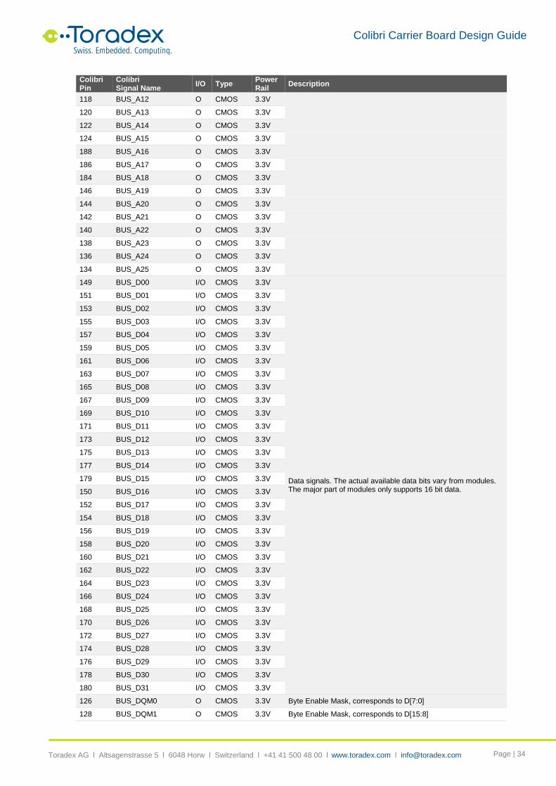
Colibri Carrier Board Design Guide
Toradex AG l Altsagenstrasse 5 l 6048 Horw l Switzerland l +41 41 500 48 00 l www.toradex.com l [email protected] Page | 34
Colibri Pin
Colibri Signal Name
I/O Type Power Rail
Description
118 BUS_A12 O CMOS 3.3V
120 BUS_A13 O CMOS 3.3V
122 BUS_A14 O CMOS 3.3V
124 BUS_A15 O CMOS 3.3V
188 BUS_A16 O CMOS 3.3V
186 BUS_A17 O CMOS 3.3V
184 BUS_A18 O CMOS 3.3V
146 BUS_A19 O CMOS 3.3V
144 BUS_A20 O CMOS 3.3V
142 BUS_A21 O CMOS 3.3V
140 BUS_A22 O CMOS 3.3V
138 BUS_A23 O CMOS 3.3V
136 BUS_A24 O CMOS 3.3V
134 BUS_A25 O CMOS 3.3V
149 BUS_D00 I/O CMOS 3.3V
Data signals. The actual available data bits vary from modules. The major part of modules only supports 16 bit data.
151 BUS_D01 I/O CMOS 3.3V
153 BUS_D02 I/O CMOS 3.3V
155 BUS_D03 I/O CMOS 3.3V
157 BUS_D04 I/O CMOS 3.3V
159 BUS_D05 I/O CMOS 3.3V
161 BUS_D06 I/O CMOS 3.3V
163 BUS_D07 I/O CMOS 3.3V
165 BUS_D08 I/O CMOS 3.3V
167 BUS_D09 I/O CMOS 3.3V
169 BUS_D10 I/O CMOS 3.3V
171 BUS_D11 I/O CMOS 3.3V
173 BUS_D12 I/O CMOS 3.3V
175 BUS_D13 I/O CMOS 3.3V
177 BUS_D14 I/O CMOS 3.3V
179 BUS_D15 I/O CMOS 3.3V
150 BUS_D16 I/O CMOS 3.3V
152 BUS_D17 I/O CMOS 3.3V
154 BUS_D18 I/O CMOS 3.3V
156 BUS_D19 I/O CMOS 3.3V
158 BUS_D20 I/O CMOS 3.3V
160 BUS_D21 I/O CMOS 3.3V
162 BUS_D22 I/O CMOS 3.3V
164 BUS_D23 I/O CMOS 3.3V
166 BUS_D24 I/O CMOS 3.3V
168 BUS_D25 I/O CMOS 3.3V
170 BUS_D26 I/O CMOS 3.3V
172 BUS_D27 I/O CMOS 3.3V
174 BUS_D28 I/O CMOS 3.3V
176 BUS_D29 I/O CMOS 3.3V
178 BUS_D30 I/O CMOS 3.3V
180 BUS_D31 I/O CMOS 3.3V
126 BUS_DQM0 O CMOS 3.3V Byte Enable Mask, corresponds to D[7:0]
128 BUS_DQM1 O CMOS 3.3V Byte Enable Mask, corresponds to D[15:8]

Colibri Carrier Board Design Guide
Toradex AG l Altsagenstrasse 5 l 6048 Horw l Switzerland l +41 41 500 48 00 l www.toradex.com l [email protected] Page | 35
Colibri Pin
Colibri Signal Name
I/O Type Power Rail
Description
130 BUS_DQM2 O CMOS 3.3V Byte Enable Mask, corresponds to D[23:16]
132 BUS_DQM3 O CMOS 3.3V Byte Enable Mask, corresponds to D[31:24]
105 BUS_nCS0 O CMOS 3.3V Chip select signals, all required chip select signals should be pulled up on the carrier board.
107 BUS_nCS1 O CMOS 3.3V
106 BUS_nCS2 O CMOS 3.3V
91 BUS_nOE O CMOS 3.3V Output Enable
99 BUS_nPWE O CMOS 3.3V Buffered Write Enable
89 BUS_nWE O CMOS 3.3V Write Enable
93 BUS_RDnWR O CMOS 3.3V Buffered Write Enable
95 BUS_RDY I CMOS 3.3V Ready/Busy/Wait signal
Table 23: Memory Bus Signals
2.17.2 Unused Memory Bus Signals Termination
All unused memory bus signals can be left unconnected. On the Colibri PXA270, the memory bus
interface is also used on the module for connecting the RAM, flash and Ethernet controller.
Therefore, the bus signal pins cannot be used for any other purpose on this module. On other
modules, it might be possible to use the unused bus signals as GPIO or for other alternative
functions.
2.18 GPIO
Many of the interface pins can also be used as general purpose input output pin (GPIO) for
alternative function. Theoretically, any unused interface pin that serves GPIO function can be used.
Since some interface pins do not provide GPIO functionality on certain Colibri modules, there is a
list of preferred GPIO pins. For compatibility reason, we recommend using the first pin on this list.
Please note that there might be additional restrictions in using the GPIO functions on certain
modules. For example, two pins share the same GPIO instance and therefore cannot be used
independently of each other on some modules. More information can be found in the datasheet of
the module.
2.18.1 Preferred GPIO Signals
Colibri Pin
I/O Type Power Rail
Description
19, 21, 23, 25, 27, 28, 29, 30, 31, 32, 33, 34, 35, 36, 37, 38, 43, 44, 45, 46, 47, 48, 49, 50, 51, 52, 53, 54, 55, 56, 57, 58, 59, 60, 61, 62, 63, 64, 65, 66, 67, 68, 69, 70, 71, 72, 73, 74, 75, 76, 78, 79, 80, 81, 82, 85, 86, 88, 90, 92, 95, 97, 98, 99, 100, 101, 102, 103, 104, 105, 106, 107, 127, 129, 131, 133, 135, 137, 190, 192, 194, 196
I/O CMOS 3.3V General purpose GPIO
Table 24: Dedicated GPIO Signals
2.18.2 Unused GPIO Termination
The GPIO signals do not need to be terminated if they are not in use.

Colibri Carrier Board Design Guide
Toradex AG l Altsagenstrasse 5 l 6048 Horw l Switzerland l +41 41 500 48 00 l www.toradex.com l [email protected] Page | 36
3 Power Management
3.1 Power Signals
3.1.1 Digital Supply Signals
Colibri Pin
Colibri Signal Name
I/O Type Power Rail
Description
42, 84,108, 148,182,198, 200 VCC I PWR 3.3V Main power supply input for the module
39, 41, 83, 109,147, 181, 197, 199
GND I PWR Common signal and power ground
40 VCC_BACKUP I PWR 3.3V RTC supply, connect this pin to 3.3V even if the internal RTC is not used
Table 25: Digital Supply Signals
3.1.2 Analogue Supply Signals
Colibri Pin
Colibri Signal Name
I/O Type Power Rail
Description
10, 12 AVDD_AUDIO I PWR 3.3V Power supply for the analogue part of the module
9, 11 VSS_AUDIO I PWR Ground for the analogue part of the module
Table 26: Analogue Supply Signals
The analogue power supply is used on the module for the analogue circuits. 3.3 Volt need to be
provided to this input even if the analogue part is not used in a design. In this case, the pins can
be connected to the main power input of the module. For a better audio quality, it is
recommended to add separate filters to the analogue power supply rail. For the best quality, a
separate power supply with linear voltage regulator is recommended.
3.1.3 Power Management Signals
Colibri Pin
Colibri Signal Name
I/O Type Power Rail
Description
26 nRESET_EXT (CTRL_RESET_MICO)
I CMOS 3.3V Active low reset input
87 nRESET_OUT (CTRL_RESET_MOCi)
O CMOS 3.3V Active low reset output
43 CTRL_WAKE_0 I CMOS 3.3V Active low main module wake input signal, needs a pull-up resistor on the baseboard if wake function is used
22 nVDD_FAULT I Analog Only available on PXA270, can be left unconnected
22 nGPIO_RESET I CMOS 3.3V Only available on PXA3xx, can be left unconnected
24 nBATT_SENSE I Analog Only available on PXA270 and PXA3xx, can be left unconnected
Table 27: Power Management Signals
In order to make the direction of the power management signals clear, the ending MICO or MOCI
are added. MICO is the abbreviation for “Module Input, Carrier board Output” while MOCI stands
for “Module Output, Carrier board Input”
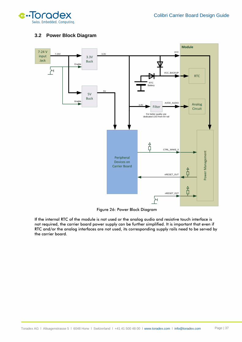
Colibri Carrier Board Design Guide
Toradex AG l Altsagenstrasse 5 l 6048 Horw l Switzerland l +41 41 500 48 00 l www.toradex.com l [email protected] Page | 37
3.2 Power Block Diagram
Figure 26: Power Block Diagram
If the internal RTC of the module is not used or the analog audio and resistive touch interface is
not required, the carrier board power supply can be further simplified. It is important that even if
RTC and/or the analog interfaces are not used, its corresponding supply rails need to be served by
the carrier board.
7-24V
Enable
Enable
Module
3.3V
RTC
nRESET_EXT
nRESET_OUT
CTRL_WAKE_0
5V
AnalogCircuit
AVDD_AUDIO
VCC_BACKUP
VCC
3.3VFilter
5VBuck
3.3V Buck
PeripheralDevices on
Carrier Board
Po
wer
Man
agem
ent
RTC
Battery
7-24 V inputJack
For better quality use
dedicated LDO from 5V rail

Colibri Carrier Board Design Guide
Toradex AG l Altsagenstrasse 5 l 6048 Horw l Switzerland l +41 41 500 48 00 l www.toradex.com l [email protected] Page | 38
Figure 27: Power Block Diagram (without RTC an analog interfaces)
7-24V
Enable
Enable
Module
3.3V
RTC
nRESET_EXT
nRESET_OUT
CTRL_WAKE_0
5V
AnalogCircuit
AVDD_AUDIO
VCC_BACKUP
VCC
5VBuck
3.3V Buck
PeripheralDevices on
Carrier Board
Po
wer
Man
agem
ent
7-24 V inputJack
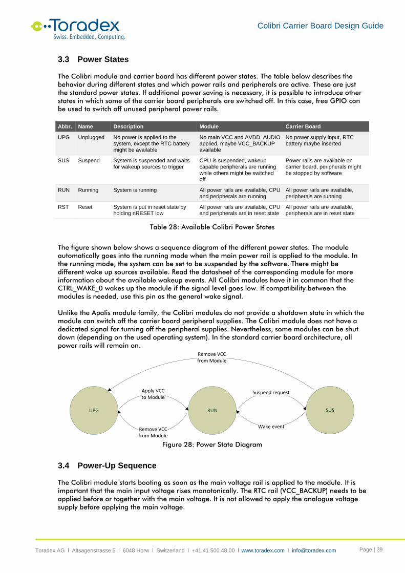
Colibri Carrier Board Design Guide
Toradex AG l Altsagenstrasse 5 l 6048 Horw l Switzerland l +41 41 500 48 00 l www.toradex.com l [email protected] Page | 39
3.3 Power States
The Colibri module and carrier board has different power states. The table below describes the
behavior during different states and which power rails and peripherals are active. These are just
the standard power states. If additional power saving is necessary, it is possible to introduce other
states in which some of the carrier board peripherals are switched off. In this case, free GPIO can
be used to switch off unused peripheral power rails.
Abbr. Name Description Module Carrier Board
UPG Unplugged No power is applied to the system, except the RTC battery might be available
No main VCC and AVDD_AUDIO applied, maybe VCC_BACKUP available
No power supply input, RTC battery maybe inserted
SUS Suspend System is suspended and waits for wakeup sources to trigger
CPU is suspended, wakeup capable peripherals are running while others might be switched off
Power rails are available on carrier board, peripherals might be stopped by software
RUN Running System is running All power rails are available, CPU and peripherals are running
All power rails are available, peripherals are running
RST Reset System is put in reset state by holding nRESET low
All power rails are available, CPU and peripherals are in reset state
All power rails are available, peripherals are in reset state
Table 28: Available Colibri Power States
The figure shown below shows a sequence diagram of the different power states. The module
automatically goes into the running mode when the main power rail is applied to the module. In
the running mode, the system can be set to be suspended by the software. There might be
different wake up sources available. Read the datasheet of the corresponding module for more
information about the available wakeup events. All Colibri modules have it in common that the
CTRL_WAKE_0 wakes up the module if the signal level goes low. If compatibility between the
modules is needed, use this pin as the general wake signal.
Unlike the Apalis module family, the Colibri modules do not provide a shutdown state in which the
module can switch off the carrier board peripheral supplies. The Colibri module does not have a
dedicated signal for turning off the peripheral supplies. Nevertheless, some modules can be shut
down (depending on the used operating system). In the standard carrier board architecture, all
power rails will remain on.
Figure 28: Power State Diagram
3.4 Power-Up Sequence
The Colibri module starts booting as soon as the main voltage rail is applied to the module. It is
important that the main input voltage rises monotonically. The RTC rail (VCC_BACKUP) needs to be
applied before or together with the main voltage. It is not allowed to apply the analogue voltage
supply before applying the main voltage.
UPG SUSRUN
Apply VCCto Module
Wake event
Suspend request
Remove VCCfrom Module
Remove VCCfrom Module

Colibri Carrier Board Design Guide
Toradex AG l Altsagenstrasse 5 l 6048 Horw l Switzerland l +41 41 500 48 00 l www.toradex.com l [email protected] Page | 40
The peripheral power rails on the carrier board needs to be ramped-up in a correct sequence. The
sequence starts normally with the highest voltage (e.g. 5V) followed by the lower voltages (e.g.
3.3V then 1.5V and so on). Peripherals normally require that a lower voltage rails is never present
if a higher rail is missing. Check the datasheet of all peripheral components on the carrier board
for a proper sequencing.
Figure 29: Power-Up Sequence
3.5 Reference Schematics
Place enough power supply bypass capacitors to the voltage inputs of the peripheral devices (see
Toradex Layout Design Guide). Place a bypass capacitor to each power input pin of the Colibri
module. Be wary of the total capacity on a voltage rail when switching the voltage. If the rails are
switched on too fast, the current peaks for charging all the bypass capacitors can be very high. This
can produce unacceptable disturbances or can trigger an overcurrent protection circuit. Maybe the
switching speed needs to be limited. The following figure shows a simple voltage rail switch circuit.
C1 and R1 limit the switching speed. The values need to be optimized according to the
requirements. It is recommended to place a bypass capacitor (C2) close to the switching transistor.
Figure 30: Simple Voltage Switch Circuit
The carrier board needs to provide the 3.3V main voltage for the module as well as all voltage rails
for the peripheral devices. Check the maximum current consumption of the Colibri modules that
VCC_BACKUP
7-27V Carrier Board in
VCC input for Module
AVDD_AUDIO for Module
Module internal Rails
Module internal Reset
nRESET_OUT
CTRL_WAKE_0
No
rma
l P
ow
er
up
(U
PG
->
RU
N)
State UPG UPG -> RUN RUN
Perpherals Rails on CB
nRESET_EXT
>0ms
>0ms
T2SI1016CX
6
21
R147K
R2100K 10nF
16V
C1
GND
C2
16V100nF
T1IRLML6401
3
1
2+V3.3_SWITCHED
GND
+V3.3
ENABLE_V3.3_SWITCHED
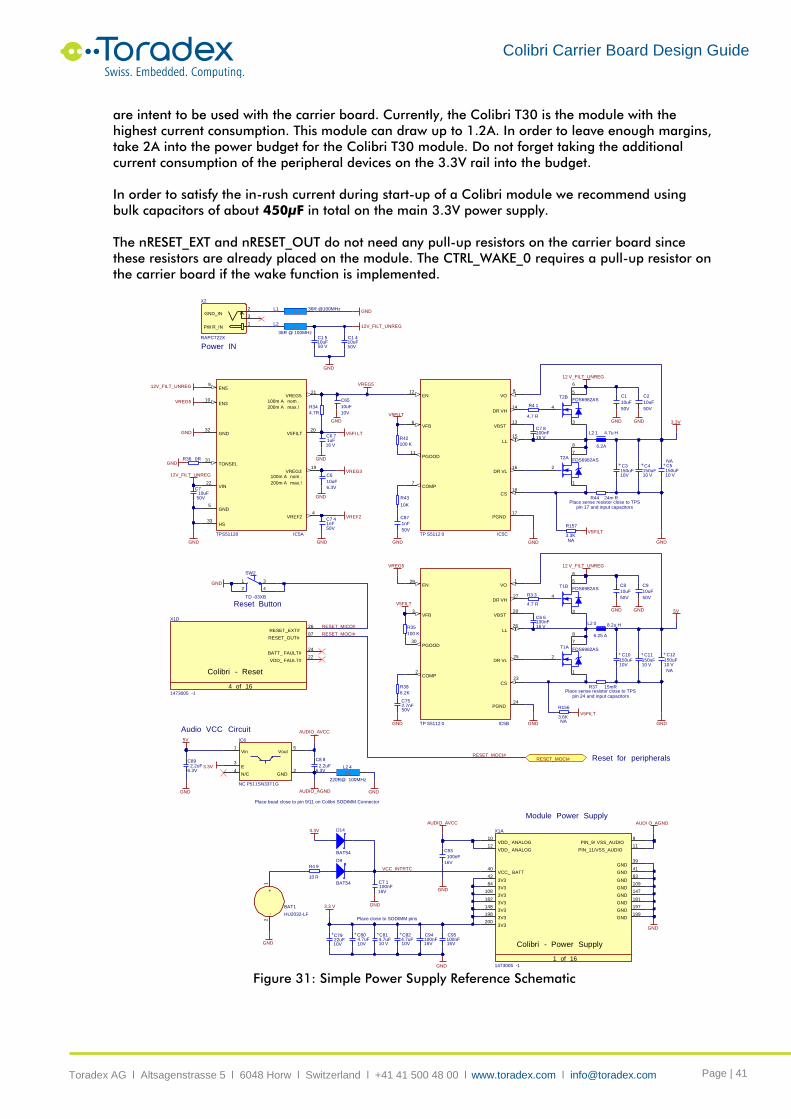
Colibri Carrier Board Design Guide
Toradex AG l Altsagenstrasse 5 l 6048 Horw l Switzerland l +41 41 500 48 00 l www.toradex.com l [email protected] Page | 41
are intent to be used with the carrier board. Currently, the Colibri T30 is the module with the
highest current consumption. This module can draw up to 1.2A. In order to leave enough margins,
take 2A into the power budget for the Colibri T30 module. Do not forget taking the additional
current consumption of the peripheral devices on the 3.3V rail into the budget.
In order to satisfy the in-rush current during start-up of a Colibri module we recommend using
bulk capacitors of about 450µF in total on the main 3.3V power supply.
The nRESET_EXT and nRESET_OUT do not need any pull-up resistors on the carrier board since
these resistors are already placed on the module. The CTRL_WAKE_0 requires a pull-up resistor on
the carrier board if the wake function is implemented.
Figure 31: Simple Power Supply Reference Schematic
GND
VREF2
GND
TPS51120
EN59
EN310
GND32
TONSEL31
VIN22
GND5
HS33
VREF2 4
VREG3
V5FILT
VREG5
100m A nom .
200m A max.!
100m A nom .
200m A max.!
IC5A
10uF
6.3V
C6
GND
VREG3
GND
1uF16 V
C6 7
GND
V5FI LT
R34
4.7R
0RR36GND
V5FILT
R35
100 K
R38
6.2K
2.7nF50V
C75
GND GND
GND
Place sense resistor close to TPS15mRR37
pin 24 and input capacitors
24m RR44
100nF16 V
C6 6
100nF16 V
C7 8
R3 3
4.7 R
R4 1
4.7 R
FDS6982AS
4
3
5
6
T1B
FDS6982AS
2
1
7
8
T1A
TP S5112 0
EN29
VFB3
PGOOD30
COMP2
LL26
VBST28
DR VH27
VO1
PGND24
CS23
DR VL25
IC5B
TP S5112 0
EN12
VFB6
PGOOD11
COMP7
LL15
VBST13
DR VH14
VO8
PGND17
CS18
DR VL16
IC5C
FDS6982AS
2
1
7
8
T2A
FDS6982AS
4
3
5
6
T2B
GND
GND
GND
GND
V5FILT
R42
100 K
GND
R43
10K
5V
3.3V
VREG510uF
10V
C65
GND
GND
GND
1nF
50V
C87
10uF
50V
C8
10uF
50V
C9
10uF
50V
C2
10uF
50V
C1
8.2u H
6.25 A
L2 0
4.7u H
6.2A
L2 1
V5FILT
R157
3.3K
R156
3.6KV5FILT
150uF10V
+C3150uF10 V
+C4 C5
1nF50V
C7 4
150uF10V
+C10150uF10 V
+C11
NA
NA
NA
NA
10uF50V
C7
VREG5
Reset Button
GND 1
2
3
4
SW2
TD -03XB
RESET_MICO#
RESET_MOCI#
RESET_MOCI#
RESET_MOCI#
RAPC722X
1
2
PW R_IN
GND_IN3
X2
36R @ 100MHz
10 AL2
10uF50 V
C1 510uF50V
C1 4
GND
12V_FILT_UNREG
36R @100MHz10 A
L1GND
12V_FILT_UNREG
12V_FILT_UNREG
12 V_FILT_UNREG
12 V_FILT_UNREG
Power IN
1473005 -1
VDD_ FAULT#22
BATT_ FAULT#24
RESET_EXT#26
RESET_OUT#87
Colibri - Reset
4 of 16
X1D
VREG5
3.3V2.2uF6.3V
C89
GND
5V
2.2uF6.3V
C8 8
2A
220R@ 100MHz
L2 4
GND
Place bead close to pin 9/11 on Colibri SODIMM Connector
Vin1
GND2
N/C4
Vout5
E3
NC P511SN33T1G
IC6
Audio VCC Circuit
GND
AUDIO_AVCC AUDI O_AGND
1473005 -1
GND39
GND41
GND83
GND109
GND147
GND181
GND197
GND199
VCC_ BATT40
3V342
3V3108
3V3182
3V3198
3V3200
3V384
3V3148
PIN_9/ VSS_AUDIO9
PIN_11/VSS_AUDIO11
Colibri - Power Supply
1 of 16
VDD_ ANALOG10
VDD_ ANALOG12
X1A
100nF16V
C7 1
GND
BAT54
D143.3V
VCC_INTRTC
Place close to SODIMM pins
GND
4.7uF10V
+C804.7uF10 V
+C814.7uF10V
+C8222uF10V
+C79
3.3 V
Module Power Supply
GND
10 R
R4 9
BAT54
D9
HU2032-LF
+1
-2
BAT1
100nF
16V
C93
GND
100nF16V
C94100nF16V
C95
Reset for peripherals
150uF10 V
+C12
150uF10 V
+
Place sense resistor close to TPSpin 17 and input capacitors
AUDIO_AVCC
AUDIO_AGND
21
20
19

Colibri Carrier Board Design Guide
Toradex AG l Altsagenstrasse 5 l 6048 Horw l Switzerland l +41 41 500 48 00 l www.toradex.com l [email protected] Page | 42
4 Mechanical and Thermal Consideration
4.1 Module Connector
The Colibri modules fit into a regular 2.5V (DDR1) SO-DIMM200 memory socket. Please note there
are two version of 200pin SO-DIMM connector available. The Colibri module is only compatible
with the variant that is designed for DDR1 modules with 2.5V. The 1.8V DDR2 variant has a
different notch position and is therefore not compatible.
There are many suitable connectors from different manufacturers available in different stacking
height. A selection of SO-DIMM200 socket manufacturers is listed below:
CONCRAFT: http://www.concraft.com.tw/connector_products_ddr.html
Morethanall Co Ltd.: http://www.morethanall.com
Tyco Electronics (AMP): http://www.te.com
NEXUS COMPONENTS GmbH: http://www.nexus-de.com
FCI http://www.fci.com
4.2 Fixation of the Module
The SO-DIMM connector features a locking mechanism which is reliable for many applications. In
order to ensure the proper connection of a module at high vibration and/or shock situations,
additional fixation might be required. The Colibri module offers different solutions for the fixation.
Figure 32: Colibri Fastener
Toradex offers Colibri Fastener for an easy to install fixation. Two fasteners are required for
holding the module. The fastener support SO-DIMM connector height of 5.2mm only. If a
connector with a different height is used, another fixation solution is required. Please note,
inserting the Colibri module is critical, if done wrong the Colibri can be damaged due mechanical
stress! More information including a module inserting guide can be found here:
http://developer.toradex.com/products/colibri-fastener
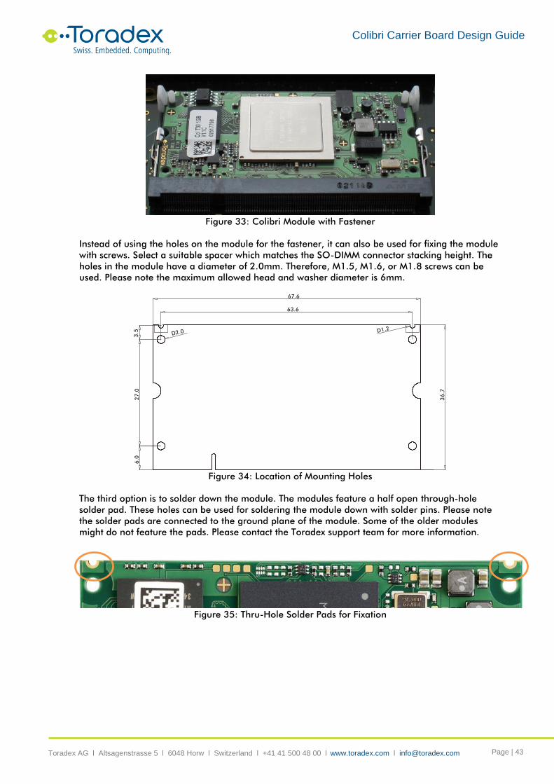
Colibri Carrier Board Design Guide
Toradex AG l Altsagenstrasse 5 l 6048 Horw l Switzerland l +41 41 500 48 00 l www.toradex.com l [email protected] Page | 43
Figure 33: Colibri Module with Fastener
Instead of using the holes on the module for the fastener, it can also be used for fixing the module
with screws. Select a suitable spacer which matches the SO-DIMM connector stacking height. The
holes in the module have a diameter of 2.0mm. Therefore, M1.5, M1.6, or M1.8 screws can be
used. Please note the maximum allowed head and washer diameter is 6mm.
Figure 34: Location of Mounting Holes
The third option is to solder down the module. The modules feature a half open through-hole
solder pad. These holes can be used for soldering the module down with solder pins. Please note
the solder pads are connected to the ground plane of the module. Some of the older modules
might do not feature the pads. Please contact the Toradex support team for more information.
Figure 35: Thru-Hole Solder Pads for Fixation
67.6
36
.7
6.0
63.6
27
.0
D2.0 D1.2
3.5

Colibri Carrier Board Design Guide
Toradex AG l Altsagenstrasse 5 l 6048 Horw l Switzerland l +41 41 500 48 00 l www.toradex.com l [email protected] Page | 44
4.3 Thermal Solution
The Colibri modules are designed to be used without additional heat spreader or heat sink. Most
of the Colibri modules feature thermal throttling mechanism. The module measures the current
temperature of the SoC. If it reaches a critical limit, it starts throttling down the CPU speed or shuts
the system completely down in order to prevent damages. Please read the corresponding
datasheets for more information to the thermal behavior.
If you only use the peak performance for a short time period, heat dissipation is less of a
problem because most of the module will reduce the power consumption when full
performance is not required.
A lower die temperature will also lower the power consumption due to smaller leakage
currents.
If you need the full CPU/Graphics performance over a long period of time, make sure that
you are able to dissipate sufficient thermal energy to the environment.
In general, more effectively the generated thermal energy is transported to the environment, the
better performance you get out of the computer module. Therefore, it might be necessary to add a
thermal solution. The best solution is to glue a suitable heat sink directly to the top of the SoC.
Since the module PCB is only 1mm thick, the board is not very stiff. Appling force to the SoC can
bend PCB which destroys the module. Therefore, pay attention when mounting a thermal solution
on the module that the module is not cracked due to bending stress.
4.4 Module Size
Figure 36: Module Dimensions Top Side (dimensions in mm)
67.6
36
.7
20
.0
R2.0
15.35
4.0
1.0
6.0
63.6
27.0
D2.0
1.0
max.3.0
max.2.2
Pin 1 Pin 39 Pin 199 Pin 1Pin 2
bottom
side (facing the carrier board)

Colibri Carrier Board Design Guide
Toradex AG l Altsagenstrasse 5 l 6048 Horw l Switzerland l +41 41 500 48 00 l www.toradex.com l [email protected] Page | 45
5 Appendix A – Physical Pin Definition and Location
The following table contains the information about the standard functions on the module edge
connector pins. Not all modules feature the complete set of standard function. Please read
carefully the function lists in the datasheet of the modules. The Toradex Pinout Designer can be a
useful tool for checking the availability of functions on certain modules. It helps configuring the pin
muxing. More information and download link can be found here:
http://developer.toradex.com/carrier-board-design/pinout-designer-tool
Module Bottom Side SO-DIMM Pin Module Top Side
Analogue Input <3> 2 1 Audio Analogue Microphone Input
Analogue Input <2> 4 3 Audio Analogue Microphone GND
Analogue Input <1> 6 5 Audio Analogue Line-In Left
Analogue Input <0> 8 7 Audio Analogue Line-In Right
Audio_Analogue VDD 10 9 Audio_Analogue GND
Audio_Analogue VDD 12 11 Audio_Analogue GND
Resistive Touch PX 14 13 Audio Analogue Headphone GND
Resistive Touch MX 16 15 Audio Analogue Headphone Left
Resistive Touch PY 18 17 Audio Analogue Headphone Right
Resistive Touch MY 20 19 UART_C RXD
VDD Fault Detect 22 21 UART_C TXD
Battery Fault Detect 24 23 UART_A DTR
nReset In 26 25 UART_A CTS, Keypad_In<0>
PWM<B> 28 27 UART_A RTS
PWM<C> 30 29 UART_A DSR
UART_B CTS 32 31 UART_A DCD
UART_B RTS 34 33 UART_A RXD
UART_B RXD 36 35 UART_A TXD
UART_B TXD 38 37 UART_A RI, Keypad_In<4>
VCC_BATT 40 39 GND
3V3 42 41 GND
LCD RGB DE 44 43 WAKEUP Source<0>, SDCard CardDetect
LCD RGB Data<7> 46 45 WAKEUP Source<1>
LCD RGB Data<9> 48 47 SDCard CLK
LCD RGB Data<11> 50 49 SDCard DAT<1>
LCD RGB Data<12> 52 51 SDCard DAT<2>
LCD RGB Data<13> 54 53 SDCard DAT<3>
LCD RGB PCLK 56 55 PS2 SDA1
LCD RGB Data<3> 58 57 LCD RGB Data<16>
LCD RGB Data<2> 60 59 PWM<A>, Camera Input Data<7>
LCD RGB Data<8> 62 61 LCD RGB Data<17>
LCD RGB Data<15> 64 63 PS2 SCL1
LCD RGB Data<14> 66 65 Camera Input Data<9>, Keypad_Out<3>, PS2 SDA2
LCD RGB HSYNC 68 67 PWM<D>, Camera Input Data<6>
LCD RGB Data<1> 70 69 PS2 SCL2
LCD RGB Data<5> 72 71 Camera Input Data<0>, LCD Back-Light GPIO
LCD RGB Data<10> 74 73
LCD RGB Data<0> 76 75 Camera Input MCLK
LCD RGB Data<4> 78 77
LCD RGB Data<6> 80 79 Camera Input Data<4>
LCD RGB VSYNC 82 81 Camera Input VSYNC
3V3 84 83 GND
SPI CS 86 85 Camera Input Data<8>, Keypad_Out<4>
SPI CLK 88 87 nReset Out
SPI RXD 90 89 nWE
SPI TXD 92 91 nOE
Colibri Carrier Board Design Guide
Toradex AG l Altsagenstrasse 5 l 6048 Horw l Switzerland l +41 41 500 48 00 l www.toradex.com l [email protected] Page | 46
Camera Input HSYNC 94 93 RDnWR
Camera Input PCLK 96 95 RDY
Camera Input Data<1> 98 97 Camera Input Data<5>
Keypad_Out<1> 100 99 nPWE
102 101 Camera Input Data<2>
104 103 Camera Input Data<3>
nCS2 106 105 nCS0
3V3 108 107 nCS1
ADDRESS8 110 109 GND
ADDRESS9 112 111 ADDRESS0
ADDRESS10 114 113 ADDRESS1
ADDRESS11 116 115 ADDRESS2
ADDRESS12 118 117 ADDRESS3
ADDRESS13 120 119 ADDRESS4
ADDRESS14 122 121 ADDRESS5
ADDRESS15 124 123 ADDRESS6
DQM0 126 125 ADDRESS7
DQM1 128 127
DQM2 130 129 USB Host Power Enable
DQM3 132 131 USB Host Over-Current Detect
ADDRESS25 134 133
ADDRESS24 136 135 SPDIF_IN
ADDRESS23 138 137 USB Client Cable Detect, SPDIF_OUT
ADDRESS22 140 139 USB Host DP
ADDRESS21 142 141 USB Host DM
ADDRESS20 144 143 USB Client DP
ADDRESS19 146 145 USB Client DM
3V3 148 147 GND
DATA16 150 149 DATA0
DATA17 152 151 DATA1
DATA18 154 153 DATA2
DATA19 156 155 DATA3
DATA20 158 157 DATA4
DATA21 160 159 DATA5
DATA22 162 161 DATA6
DATA23 164 163 DATA7
DATA24 166 165 DATA8
DATA25 168 167 DATA9
DATA26 170 169 DATA10
DATA27 172 171 DATA11
DATA28 174 173 DATA12
DATA29 176 175 DATA13
DATA30 178 177 DATA14
DATA31 180 179 DATA15
3V3 182 181 GND
ADDRESS18 184 183 Ethernet Link/Activity Status
ADDRESS17 186 185 Ethernet Speed Status
ADDRESS16 188 187 Ethernet TXO-
SDCard CMD 190 189 Ethernet TXO+
SDCard DAT<0> 192 191 Ethernet GND
I2C SDA 194 193 Ethernet RXI-
I2C SCL 196 195 Ethernet RXI+
3V3 198 197 GND
3V3 200 199 GND
Table 29: Physical Pin Definition and Location
Colibri Carrier Board Design Guide
Toradex AG l Altsagenstrasse 5 l 6048 Horw l Switzerland l +41 41 500 48 00 l www.toradex.com l [email protected] Page | 47
DISCLAIMER:
Copyright © Toradex AG. All rights reserved. All data is for information purposes only and not
guaranteed for legal purposes. Information has been carefully checked and is believed to be
accurate; however, no responsibility is assumed for inaccuracies.
Brand and product names are trademarks or registered trademarks of their respective owners.
Specifications are subject to change without notice.