components, packaging, and manufacturing technology
TRANSCRIPT

1September 2010 IEEE CPMT Society Newsletter
President’sColumn....
greatdealofmytimeoverthelastfewmonthswastakenupwith organizingESTC2010.The conference’s five daysof presentations and workshops finally took place last
weekand,exhaustedbuthappy,Icanreportthattheeventwasahugesuccess.With480participantsandanextensiveandexcitingcoreandsupplementarytechnicalprogram,Ibelievewesuccess-fullyputtogetheramemorableconferenceforallparticipants.Thefeedbacksofarhasbeengreatand,ofcourse,attheendoftheday,it was the participation of all the delegates and exhibitors thatmadethedifference.
The3DWLPworkshopwasclearlyahighlightofthetechnicalprogram.Fromthebuzzprior to theworkshopand thedynamiccontributionsduringitscourse,itbecameobviousthat3Dpackag-ingiscurrentlythefocusofalotofattentioninR&Ddepartmentsaroundtheworld.Architecture,aswellasmaterialandequipment,arekey topics in3DWLPandwecandefinitelyexpect tohearmore on this in the foreseeable future.The panel discussion on“Embedding Technologies“ also saw hot discussion. This wasonlytobeexpectedasthetechnologyisverysensitivetochangesinthesupplychain.Whilethediscussionhighlightedmanypress-ingissuesandwasagreatchanceforplayersintheareatoconnect,alotmoreexchangeofideasonhowtotacklechallengesinthisareawillbenecessary.
Whiletheweathergodsdidnotsmileonusthistime,thecon-ference’slocationintheheartofoldBerlin,justaroundthecornerfromCheckpointCharlie, theTiergartenpark and theBranden-burgerGate,wasstillagreatopportunitytoexplorethecityfor
RolfAschenbrennerPresident,IEEECPMTSociety
Fraunhofer-Institut,Berlin,[email protected]
NEWSLETTER SUBMISSION DEADLINES:
15 November 201015 February 2011
15 May 201115 August 2011
Submit all material to [email protected]
Components, Packaging,and Manufacturing Technology Society Newsletter
THE GLOBAL SOCIETY FOR MICROELECTRONICS SYSTEMS PACKAGING
VOL. 33 NO. 4, SEPTEMBER 2010, ISSN 1077-2999 www.cpmt.org www.ewh.ieee.org/soc/cpmt/newsletter
(continued on page 3)
A

2 IEEE CPMT Society Newsletter September 2010
CPMT OfficersPresident: RolfAschenbrenner +49-30-46403-164VP (Technical): N.RaoBonda +1-480-413-6121VP (Conferences): JieXue +603-896-5337VP (Publications): R.WayneJohnson +1-334-844-1880VP (Education): KittyPearsall +1-512-838-7215VP (Finance): ThomasG.ReynoldsIII +1-850-897-7323Sr. Past Pres.: PhilGarrou +1-919-248-9261Jr. Past Pres.: WilliamT.Chen +1-408-986-6505Executive Director: MarshaTickman +1-732-562-5529
Elected Board Members2010: Eric O. Beyne, Steve J. Bezuk, Eric Perfecto, Dongkai Shangguan,
EphraimSuhirandC.P.Wong2011: VasudevaAtluri,KoneruRamakrishna,PatrickThompson,PaulWesling,
Klaus-JurgenWolter,andKishioYokkouchi2012: Chris Bailey, Daniel Donahoe, Paul D. Franzon, S-W (Ricky) Lee,
Kwang-LungLin,andLeonardW.Schaper
CPMT Society NewsletterEditor-in-Chief: Vacant
CPMT Archival PublicationsPublications VP: R.WayneJohnson,+1-334-844-1880;[email protected], CPMT Transactions:AvramBar-Cohen,Univ.ofMaryland,+1-301-405-3173,[email protected] on Components & Pkg. Technologies, Editors in Chief: RickyS.W.Lee,HongKongUnivofScience&Technology,+852-2358-7203;[email protected],Freescale,Inc.,+1-512-933-2555;[email protected] on Advanced Packaging, Editors in Chief:G.Subbarayan,PurdueUniversity,MechanicalEngineeringDept.,+1-765-494-9770;[email protected]éE.Schutt-Ainé,UniversityofIllinoisatUrbana-Champaign,+1-217-244-7279,[email protected] on Electronics Pkg. Manufacturing, Editor in Chief:R.WayneJohnson,+1-334-844-1880,[email protected]
Technical Committee ChairsTC-Assy - IC and Package Assembly:MartinGoetz,IBM,+1-919-486-2409,[email protected] - Environmental Stress & Reliability Test:JohnE.Proulx,GMATC,+1-310-257-3714,[email protected] - Electrical Contacts, Connectors and Cables:JerryWitter,ChugaiUSAInc.,+1-847-244-6025,[email protected] - Education:RaoR.Tummala,GeorgiaTech.,+1-404-894-9097,[email protected] - Electrical Design, Modeling and Simulation:MadhavanSwaminathan,GeorgiaTech,+1-404-894-3340,[email protected] - Manufacturing - Design & Process:WalterJ.Trybula,SEMATECH,+1-512-356-3306,[email protected] - Green Electronics Manufacturing and Packaging:NilsF.Nissen,IZM,Berlin,+49-30-46403-139,[email protected] - High Density PWB Packaging:YoshitakaFukuoka,Weisti,+81-3-3475-0755,[email protected] - Materials:RajenChanchani,SandiaLabs,+1-505-844-3482,[email protected] - MEMS and Sensor Packaging:EricJung,IZM,Berlin,+49-30-46403-161,[email protected] - Nano Packaging:RaoTummala,GeorgiaTech.,+1-404-894-9097,[email protected] - Fiber Optics & Photonics:VacantTC-PEP - Power Electronics Packaging:DouglasHopkins,SUNYBuffalo,+1-607-729-9949,[email protected]+W - RF and Wireless:CraigA.Gaw,Freescale,+1-480-413-5920,[email protected] - Systems Packaging:CianOMathuna,+353-21-4904350,[email protected]
TC-Test - Electrical Test:BruceKim,UnivofAlabama,+1-205-348-4972,[email protected] - Thermal Management & Thermomech. Design:TonyMak,DallasSemiconductor,+1-972-371-4364,[email protected] - Wafer Level Packaging:MichaelToepper,IZM,Berlin,+49-30-46403-603,[email protected]
Strategic Program DirectorsAwards and Recognition:PatrickThompson,[email protected]:JieXue,[email protected] Integration:C.P.Wong,[email protected] Programs:KittyPearsall,[email protected] Chapters and Membership:EricPerfecto,[email protected]:R.WayneJohnson,[email protected] Programs:ChrisBailey,ChrisBailey,[email protected] Programs:N.RaoBonda,[email protected] 8 Programs:[email protected] 10 Programs:CharlesLee,[email protected]
Standing Committee ChairsAwards:PatrickThompson,[email protected] Development:EricPerfecto,[email protected] and Bylaws:TonyMak,[email protected] Lecturers:KittyPearsall,[email protected] Activities:VacantFellows Evaluation:CPWong,[email protected] Search:RaoTummala,[email protected]:WilliamChen,[email protected] Range / Strategic Planning:PhilipE.Garrou,pgarrou/[email protected]:EricPerfecto,[email protected]:WilliamChen,[email protected]
Distinguished LecturersProgram Director:KittyPearsall,[email protected]:AlbertF.Puttlitz,Ph.D.,AvramBar-Cohen,Ph.D.,H.AnthonyChan,Ph.D.,RajenChanchani,Ph.D.,WilliamT.Chen,Ph.D.,BadihEl-Kareh,Ph.D.,XuejunFan,Ph.D.,PaulD.Franzon,Ph.D.,PhilipGarrou,Ph.D.,GeorgeG.Har-man,Ph.D.,R.WayneJohnson,Ph.D.,GeorgeA.Katopis,Ph.D., JormaKaleviKivilahti, D.Sc., John H. Lau, Ph.D., Michael Lebby, Ph.D, Ning-Cheng Lee,Ph.D.,S.W.RickyLee,Ph.D.,JohanLiu,Ph.D.,JamesE.Morris,Ph.D.,KyungW.Paik,Ph.D.,T.PaulParker,MichaelPecht,Ph.D.,KarlJ.Puttlitz,Ph.D.,BahgatSammakia,Ph.D.,DongkaiShangguan,Ph.D.,NihalSinnadurai,Ph.D.,EphraimSuhir, Ph.D., Yong-Khim Swee, Yutaka Tsukada, Ph.D., Rao Tummala, Ph.D.,WalterTrybula,Ph.D.,E.JanVardaman,PaulWesling,CPWong,Ph.D.,RalphW.WyndrumJr.,Ph.D.,KishioYokouchi,Ph.D.
Chapters and Student BranchesRefertowww.cpmt.orgforCPMTSocietyChaptersandStudentBrancheslist
IEEEComponents,Packaging,andManufacturingTechnologySocietyNewsletterispublishedquarterlybytheComponents,Packaging,andManufacturingTechnol-ogySocietyoftheInstituteofElectricalandElectronicsEngineers,Inc.Headquar-ters:3ParkAvenue,17thFloor,NewYork,NY10016-5997.US$1.00permemberperyearisincludedinSocietyfeeforeachmemberoftheComponents,Packaging,andManufacturingTechnologySociety.PrintedinU.S.A.Periodicalspostagepaidat New York, NY, and at additional mailing offices. Postmaster: Send addresschangestoIEEECPMTNewsletter,IEEE445HoesLane,Piscataway,NJ08854.Allrightsreserved,copyright(c)2005bytheCPMTSocietyofIEEE.AuthorsandArtistsgivenfullpermissionforfurtheruseoftheircontributions.ForcirculationinformationcallIEEECustomerService800-701-4333,orFAX908-981-9667.
CPMT Members-Only Web(www.cpmt.org/mem/)
(See printed version for UserName and Password)
IEEE prohibits discrimination, harassment, and bullying. For more information,visit http://www.ieee.org/web/aboutus/whatis/policies/p9-26.html.

3September 2010 IEEE CPMT Society Newsletter
the delegates who managed to tear themselves away from thetechnicalprogram.Ialsounderstandthatallenjoyedthesupport-ingprogram,particularly thegaladinner atMeilenwerk,whichwasagreatopportunityforsomequalitytimenotonlywiththeother delegates, but also some outstanding automobile technol-ogy.Forthoseofyouwhocouldnotattendtheconference,besuretocheckthemoredetailedoverviewofESTC2010furtheroninthisnewsletter.
The succession of conferences and events continues, withpreparationforthe61stECTC,takingplaceinFlorida,currentlyunderway.Aswithourevents, I encourageyou toget involved,
andremindyouthatabstractsubmissionsarestillopenuntilmid-October,enoughtimetopackageyourlatestresearchandhopefullyjoinusnextJune.ECTCisoneoftheindustry’slongestrunningevents, havingbeenheld in one formor another since1950. InJune,thejointsponsorshipbytheIEEEComponents,PackagingandManufacturingSociety (CPMT)and theECA(formerly theEIA) endedwith IEEEbuyingout their long-termpartner.ThisleavesCPMTasthesolesponsor.However,weareworkinghardtoensurethatconferenceremainsthequalityeventithastradition-allybeen,andbelievethatthislogisticalchangeshouldpassunno-ticedbyboththeattendeesandtheECTCprogramcommittee.
President's Column.... (cont.)
CPMT ELECTION BEGINS ON 24 SEPTEMBER—PLEASE VOTE By
29 OCTOBER
The IEEE Components, Packaging, and ManufacturingTechnologySocietyConstitutionandBylawsprovidethatthe membership shall elect each year
sixMembers-at-LargetotheSocietyBoardofGovernorstoserveathree-yearterm.
Members-at-large will be elected toachievetotalsproportionatetothegeographicdistribution of CPMT members. For 2010,thistranslatesasfollows:
Regions 1-6, 7 and 9 (US, Canada, SouthandCentralAmerica): elect 5 members Candidates: Xuejun Fan, Ning-Cheng
Lee, Debendra Mallik, James Morris,Eric Perfecto, Bahgat Sammakia,DongkaiShangguan,JeanTrewhella
Region8(Europe,Africa,MiddleEast): elect 1 member Candidates: JanFelba,ToniMattila,GillesPoupon
Region10(Asia/Pacific):no members to be elected
Thesixnewly-electedMembers-at-Largewill joincontinuingMembers-at-Large(shownbelow)ontheBoardofGovernors:
FromRegions1-6,7and9:VasudevaAtluri,DanielDonahoe,Paul Franzon, Koneru Ramakrishna, Len Schaper, PatrickThompson,PaulWesling,
FromRegion8:ChrisBailey,KlausJürgen-Wolter From Region 10: Ricky Lee, Kwang-Lung Lin, Kishio
Yokouchi
The Nominations Committee included the CPMT StrategicProgram Director, Region 8. The Strategic Program Director
workedwithvolunteer leaders inhisRegionto identify a high-quality slate of candidatesfromthatRegion.
Voting members will elect Members-at-Large from within their respective Regiononly – that is, members in Region 8 willvote for Members-at-Large from Region 8only,etc.
Thisyear’selectioncontinuestooffertheopportunitytocastyourballotelectronically.YouwillneedyourIEEEWebAccountuser-name/passwordtoaccesstheballotandcastyour vote. This is the same account infor-mationusedtoaccessIEEEonlineservices
suchasrenewingyourmembership,myIEEE,andXplore.Itisrecommended thatyou testyourwebaccount access atwww.ieee.org/myieee to avoid any potential problems with access-ingyourballot.Ifyoudonotrecallyourwebaccountinforma-tion, you may go to: www.ieee.org/web/accounts to [email protected]+18006784333(USA/Canada)or+17329810060(Worldwide).
If you have any questions about the IEEE CPMT Soci-ety voting process, please contact [email protected] or+17325623904.
CPMTSocietyNews....
4 IEEE CPMT Society Newsletter September 2010
JORMA KIVILAHTI FIRST RECIPIENT OF IEEE CPMT REGION 8 AWARD
For establishing the IEEE CPMT Finland Chap-ter, developing programs to serve local CPMT members and the profession and building strong collaborations and networks within the region.
ProfessorJormaKivilahtibecamethefirstrecipi-ent of the CPMT Society Regional Contribu-tionsAwardforRegion8(Europe,MiddleEast,
Africa).TheAwardwasestablishedtorecognizesignificantandoutstandingleadershipand contributionstothegrowthandimpactofCPMTprogramsandactivitiesattheRegionlevel.
The presentation took place at the recentElectronicsSystemIntegrationConference(ESTC)inBerlin.
ProfessorKivilahtiisanIEEEFellow,aCPMTDistinguishedLecturer,andrecipientofthe2006CPMT“OutstandingSustained
Technical Contribution Award”. Professor Kivilahti headed thelaboratoryofElectronicsProductionandtheGraduateSchoolofElectronicsManufacturingatHelsinkiUniversityofTechnology,wherehisR&Dprimarilycoveredtheintegrationandreliabilityofelectronics.Hisnumerousmajor researchprojects inelectronicsmanufacturingandreliability,hundredsofscientificand techno-logicalpapersandseveralpatentsplayedamajorroleinshapingFinland’smicroelectronicsindustry.
ProfessorKivilahtiwasextremelyactiveinCPMTandthisawardrecognizeshisestablishmentoftheFinlandIEEECPMTChapterin1998.HeworkedhardandcloselywiththeNordiccountries to initiate theChapterandwentontoheadit for itsfirst three years. His term was impressive. He was the driv-ing force behind high quality seminars with lecturers world-wide andhe established several highly effective networks fortheCPMTSocietyintheNordics.TheChapterremainsstrongtodaythankstoProfKivilahti’ssustainedcontributiontoCPMTinRegion8.
CALL FOR NOMINATIONS FOR THE 2011 CPMT SOCIETy AWARDS
NOMINATIONS DUE By JANUARy 31, 2011
Hey!! It is that time of year and this is a Call forAction!!!! Don’t wait unti the last minute and MISSOUT on a great opportunity to recognize a peer or a
co-worker for their contribution to the CPMT Society and/ortheirtechnicalcommunity.MakeacommitmentTODAYtoputyourthinkingcapsonandthinkofthoseindividualsthatshouldberecognized!IamsurethatyouknowwhohasgoneaboveandbeyondintheircontributiontotheirtechnicalcommunityandtotheCPMTSociety.Don’thesitatetoputtheirnamesforth.TheAwards Committee is currently accepting nominations for the2011 CPMT Awards. All nomination packages are due byJanuary31,2011.Winnerswillbenotifiedby31March2011and the awards will be presented at the 61th ElectronicComponents and Technology Conference, May 31st–June 3rd
2011,inOrlando,Florida,USA.AcurrentnominationformcanbefoundontheCPMTwebsiteattheAwardslinkbyaccessingthe following url http://www.cpmt.org/awards/index.html. Welookforward to receivingmanynominations inall thecatego-rieslistedbelow:
CPMTSocietyoffersthefollowing5awardsforthepurposeofrecognizingoutstandingserviceandcontributionstofurtheringtheprofessionalpurposesoftheCPMTSociety.
1) David Feldman Outstanding Contribution Award: Thisawardrecognizesoutstandingcontributionstothefieldsencom-passedbytheCPMTSocietythroughexecutiveormanagerialdirections.
Prize:$2,500andCertificate Basis for Judging:Contributionstotheorganizationorenter-
prisesconnectedwiththefield, toCPMTChapter,SectionorBoardofGovernorsactivities, and to the fieldsencompassedbytheCPMTSociety.
Eligibility: RecipientmusthavebeenamemberofIEEEandCPMTforthepastfive(5)years,including2010.
2) Outstanding Sustained Technical Contributions Award: Torecognize outstanding sustained and continuing contributionsto the technology in fields encompassed by the CPMTSociety.
Prize:$2,500andCertificate Basis for Judging:Technicalcontributionsmustbesustained
andcontinuingoveraperiodofatleastfive(5)andpreferably10years.Onemajorcontributionwillnotqualify.Contributionsmust be documented by open literature publications such aspapers,patents,booksandreports(availabletothepublic).
Eligibility:MusthavebeenamemberoftheIEEEandCPMTSocietyforthepastthree(3)years,including2010.
3) Electronics Manufacturing Technology Award: To recog-nize major contributions to Electronic ManufacturingTechnologyinfieldsencompassedbytheCPMTSociety.
Prize:$2,500andCertificate Basis for Judging: Contributions may include technical de-
velopmentof,ormanagement (directing)ofmajornewelec-tronicmanufacturingprocesses;significantlyincreasingyieldand/orreliabilityofestablishedmanufacturingprocesses,etc.Work in the management of CPMT conferences or its BoGmaybecontributorybutnotsufficienttoreceivetheaward.
Eligibility: No need to be a member of IEEE and CPMTSociety.
4) Exceptional Technical Achievement Award: To recognizeanindividual,orgroupofindividuals(nomorethanthree),forexceptional technical achievement in the fields encompassedbytheCPMTSociety.
Prize:$2,500andaCertificate. Basis for Judging:Technicalcontributionsof thenominee(s)
must be such that they are considered to be exceptional, notachieved by most members. A single major contribution willqualify for thisaward.Thecontributioncouldbea significantinvention, introduction of a significantly new and important

5September 2010 IEEE CPMT Society Newsletter
technology or product (in which case, the nominee may be ateamleader),orsignificantworkthatadvancesthestate-of-the-artinCPMT’sfieldofinterest.Thetechnicalcontributionsmustbedocumentedbyopenliteraturepublicationssuchaspapers,patents,books,andreports (available to thepublic).Technicalrecognition and awards from the organization employing theindividual as well as awards from other IEEE and non-IEEEtechnicalsocietiesmayalsobecontributory.
Eligibility: Recipient(s) must have been a member of IEEEandCPMTforthepastthree(3)years,including2010.TherearenorequirementsforservicetotheIEEEorCPMTSociety.
5) Outstanding young Engineer Award: To recognize out-standingcontributionstothefieldsencompassedbytheCPMTSociety through invention, technical development, publica-tions,ornewproductimplementation.
Prize:$1,500andCertificateplusoneyearfreemembershipinCPMTwithallCPMTTransactions.
Basis for Judging: Technical contributions through patentinvention,contributionstotechnologyorproductdevelopmentwithin theCPMTFieldofInterest.Mayencompassmanage-ment (directing) of significant new product introduction orimplementation of major new electronic manufacturing pro-cesses; significantly increasing yield and/or reliability ofestablished manufacturing processes. Contributions to theSociety, through the BoG, Conferences, Chapters, etc., willalsobeconsidered.Proofofcontributionsmayconsistofopenliterature publications (preferred) such as papers, patents,books,andreports(availabletothepublic).Atleastthree(3)lettersfrompeersandmanagementatthenominee’splaceof
employmentattestingtotheaccomplishment(s)canbeaccept-edinlieuofpublications.
Eligibility:MusthavebeenamemberoftheIEEEandCPMT(membergradeorabove)forthepastthree(3)years,including2009,andmustbe35yearsofage,oryounger,onDecember31st, 2010. Please provide Date of Birth (Month/Year) toensureeligibility.
Guidelines for Nominators:• Minimumthreereferencelettersmustbesubmittedinsupport
ofallnominations.ReferenceletterscanbeprovidedbyIEEE/CPMTmembersandnon-members.
• Pastrecipientsofanawardarenoteligibletoreceivethatsameaward.Forlistofpastawardees,seetheCPMTSocietyHomepage(http://www.cpmt.org/awards).
• Anindividualmaysubmitonlyonenominationperawardbutmaysubmitnominationsformorethanoneaward.
• It is the responsibility of the nominator to provide qualitydocumentation to assist the Awards Committee in evaluatingthecandidate.
• Please send nominations to CPMT Society Director, Awardsbye-mailormail:
PatrickThompsonTexasInstruments,Inc.MS940,POBox655012Dallas,TX75265USAPhone:+1-972-995-7660Email address: [email protected]
Anytechnologist–member or non-member–iswelcometoreceivealertswhenupcomingissuesofourCPMTTransactionsarepostedtotheIEEE’sXploredatabaseandallthepapersareavailablefordownloading.Thisisahandywaytoscantheissue’sTableofContentsandquicklylearnaboutnovelapproachestopackaging,modeling,reliability,materials,assemblyandothertopics.
Thewebsitelinkis:ieeexplore.ieee.org/xpl/tocalerts_signup.jsp
IfyoualreadyhaveanIEEEwebaccount,youmaysign inandselect those journalsyouwish to track. Ifyoudon’thaveanaccount,allittakesisyournameandemailaddress!ThensimplyclicktheAlertStatusboxnexttothejournalsyouwishtomoni-tor.YouwillreceiveanemaileachquarterwhenthatjournalispostedtoXplore.
Similarly,ifyouprefertoreceiveinformationbyRSSfeed,youmayaddourjournals’feedstoyourReader.You’llgetalistingofthepapersinthatissue,alongwithfullabstractsandalinkfordownloadingthepaper.TheRSSlinksareshownonthissamewebpage.
Herearethejournalswesuggestyouselectformonitoring:
➥ AdvancedPackaging,IEEETranson➥ ComponentsandPackagingTechnologies,IEEETranson➥ ElectronicsPackagingManufacturing,IEEETranson

6 IEEE CPMT Society Newsletter September 2010
COMING IN 2011 – NEW OPTIONS FOR SUBSCRIBERS TO CPMT TRANSACTIONS
s previously announced, beginning in January 2011, theCPMT Society will launch the IEEE Transactions on Components, Packaging, and Manufacturing Technology.
This monthly periodical is a consolidation of the three currentCPMTSocietyTransactions:Transactions on Advanced Packaging, Transactions on Components and Packaging Technologies and Transactions on Electronics Packaging Manufacturing.
SubscriberswillnowhaveaccesstoallCPMTarchivaltech-nicalcontentinonemonthlypublication(12issuesannually)—withnoworryofmissingpapersofinterest thatmayhavebeenpublishedinoneoftheotherCPMTTransactionstowhichtheydidn’tsubscribe.
Additionally,subscriberswillhavenewoptionsthatallowthemtomanage their subscription feesand themanner inwhich they
receivethenewTransactions—bychoosingelectroniconly(onlineviaIEEEXplore),printonly,orcombo(electronicandprint).
Those who currently subscribe to at least one of the currentCPMT Transactions will receive a 2011 IEEE renewal invoicethatincludesthenewIEEE Transactions on Components, Packag-ing, and Manufacturing Technology—which replaces thecurrentCPMTsubscription(s).
The default media type for Member subscribers will becombo (electronic and print). Those who prefer print only orelectroniconlycanmakethischangewhentheycompletetheirrenewal. For Student subscribers, the default media will beelectroniconly.
TheconsolidatedTransactions,willbepublishedonlinemonthly(12issuesannually).Printissueswillbepublishedbimonthly(sixissuesannually)andcombinetwomonthsofonlineissues.
Questionsandfeedbackonthesechangesarewelcome;[email protected].
PublicationNews....
A
HAVE yOU READ THEM? THE MOST DOWNLOADED CPMT PAPERS
WhatmightyoubemissingintheCPMTliterature?Following is a list of the top CPMT Transactions
papers downloaded in July 2010. Subscribers canaccesstheseandotherpapersonIEEEXplore.
IEEETransactionsonAdvancedPackaging
1) Effects of Warpage on Fatigue Reliability of Solder Bumps: Experimental and Analytical Studies, Wei Tan;Ume, I.C.; Ying Hung; Wu, C.F.J.; Issue Date: May 2010Page(s):314–322Out-of-plane displacement (warpage) has been a major ther-
momechanicalreliabilityconcernforboard-levelelectronicpack-ages.Printedwiringboard(PWB)andcomponentwarpageresultsprincipallyfromcoefficientofthermalexpansionmismatchamongthematerialsthatmakeupthePWBassembly(PWBA).Warpageoccurring during surface-mount assembly reflow processes andnormaloperationsmayleadtoseveresolderbumpreliabilityprob-lems. In this research, the effect of initial PWB warpage on thelowcyclethermalfatiguereliabilityofthesolderbumpsinplasticballgridarray(PBGA)packageswasstudiedusingexperimentalandanalyticalmethods.Areal-timeprojectionmoire¿warpagemeasurementsystemwasusedtomeasurethesurfacetopologyofPWBAsamplesatdifferenttemperatures.Thethermalfatiguereli-abilityofsolderbumpswasevaluatedfromexperimental thermalcycling tests and finite element simulation results. Three-dimen-sional(3-D)modelsofPWBAswithvaryingboardwarpagewereusedtoestimatethesolderbumpfatiguelifefordifferenttypesofPBGAsmountedonPWBs.InordertoimprovetheaccuracyofFEresults, theprojectionmoire¿methodwasused tomeasure the
initialwarpageofPWBs,andthiswarpagewasusedasageometricinputtothefiniteelementmethod.Thesimulationresultswerevali-datedandcorrelatedwiththeexperimentalresultsobtainedusingtheprojectionmoire¿techniqueandacceleratedthermalcyclingtests.AnadvancedpredictionmodelwasgeneratedtopredictboardlevelsolderbumpfatiguelifebasedontheinitialPWBwarpage,packagedimensionsandlocations,andsolderbumpmaterials.
2) Guaranteed Passive Parameterized Admittance-Based MacromodelingFerranti,F.;Knockaert,L.;Dhaene,T.;IssueDate:Aug.2010Page(s):623–629Weproposeanovelparametricmacromodeling technique for
admittance and impedance input-output representations parame-terizedbydesignvariablessuchasgeometricallayoutorsubstratefeatures. It is able to build accurate multivariate macromodelsthatarestableandpassiveintheentiredesignspace.Anefficientcombination of rational identification and interpolation schemesbasedonaclassofpositiveinterpolationoperators,ensuresoverallstabilityandpassivityof theparametricmacromodel.Numericalexamplesvalidatetheproposedapproachonpracticalapplicationcases
3) Packaging of Dual-Mode Wireless Communication Module Using RF/Optoelectronic Devices With Shared Functional Components Jun Liao; Juan Zeng; Shengling Deng;Boryssenko, A.O.; Joyner, V.M.; Huang, Z.R.; Issue Date: May2010Page(s):323–332Thispaperreportsthedesign,fabrication,andtestingofacom-
pact radio-frequency (RF)/ free space optical (FSO) dual modewirelesscommunicationsystem.Amodifiedsplitdual-directorqua-si-Yagiantennaisintegratedwithopticaltransmitterandreceiverbysharinglayoutstructuralcomponents.Baredievertical-cavitysurface-emitting laser (VCSEL)andP-i-Nphotodiode (PIN)are

7September 2010 IEEE CPMT Society Newsletter
placedonantennadirectorpadsand wirebondedtoprintedcircuitboard (PCB)-mounted laserdriverand transimpedanceamplifier(TIA) circuits. Detailed analysis of coupling between RF chan-nelandassociatedelectricalconnections for theFSOchannel ispresentedusingcommercialsimulationtoolstopredictitsimpactonlinkdegradation.AlthoughcrosstalkappearsbetweenRFandopticalchannels,theprototypedsystemdemonstrateddual-modehigh-ratecommunicationcapabilitywithmeasured2.5Gb/sdatarateinFSOlink.VariationsinRFsubsystemfeaturesduetocou-plingfromtheFSOsubsystemisestimatedthroughradiationpat-ternmeasurementusingnear-fieldscanner.
TransactionsonComponentsandPackagingTechnologies
1) Analytical and Numerical Modeling of the Thermal Performance of Three-Dimensional Integrated Circuits Jain, A.; Jones, R.E.; Chatterjee, R.; Pozder, S.; Issue Date:March2010Page(s):56–63Three-dimensional(3D)interconnectiontechnologyofferssev-
eralelectricaladvantages,includingreducedsignaldelay,reducedinterconnect power, and design flexibility. 3D integration reliesonthrough-siliconvias(TSVs)andthebondingofmultipleactivelayerstostackseveraldieorwaferscontainingintegratedcircuits(ICs) and provide direct electrical interconnection between thestackedstrata.Whilethisapproachprovidesseveralelectricalben-efits,italsoofferssignificantchallengesinthermalmanagement.Whilesomeworkhasbeendoneinthepastinthisfield,acompre-hensive treatment is still lacking. In thecurrentwork,analyticalandfinite-elementmodelsofheat transferinstacked3DICsaredeveloped.Themodelsareusedtoinvestigatethelimitsofthermalfeasibilityof3Delectronics and todetermine the improvementsrequiredintraditionalpackaginginordertoaccommodate3DICs.Ananalyticalmodelfortemperaturedistributioninamultidiestackwithmultipleheatsources isdeveloped.Theanalyticalmodel isusedtoextendthetraditionalconceptofasingle-valuedjunction-to-airthermalresistanceinanICtothermalresistanceandthermalsensitivitymatricesfora3DIC.Theimpactofvariousgeometricparametersandthermophysicalpropertiesonthermalperformanceofa3DICisinvestigated.Itisshownthatpackageandheatsinkthermalresistancesplayamoreimportantroleindeterminingtem-peraturerisecomparedtothermalresistancesintrinsictothemul-tidie stack.The improvement required inpackage andheat sinkthermalresistancesfora3Dlogic-on-memoryimplementationtobethermallyfeasibleisquantified.Anincreaseinmaximumtem-peratureina3DICcomparedtoanequivalentsystem-in-package(SiP)ispredicted.Thisincreaseisfoundtobemainlyduetothereducedchipfootprint.Theincreasedmemorydietemperatureincase of memory-on-logic integration compared to a SiP imple-mentation is identified tobeasig-nificant thermalmanagementchallengeinthefuture.Theresultspresentedinthispapermaybeusefulinthedevelopmentofthermaldesignguidelinesfor3DICs,whichareexpectedtohelpmaximizetheelectricalbenefitsof3Dtechnologywithoutexacerbatingthermalmanagementissueswhenimplementedinearly-stageelectricaldesignandlayouttools.
2) Dynamic lithium-ion battery model for system simulationLijunGao;ShengyiLiu;Dougal,R.AIssueDate:September2002Page(s):495–505
Presentshereacompletedynamicmodelofalithiumionbat-tery that is suitable for virtual-prototyping of portable battery-poweredsystems.Themodelaccountsfornonlinearequilibriumpotentials, rate- and temperature-dependencies, thermal effectsandresponsetotransientpowerdemand.Themodelisbasedonpubliclyavailabledatasuchasthemanufacturers’datasheets.TheSonyUS18650 isusedasanexample.Themodeloutputagreesbothwithmanufacturer’sdataandwithexperimentalresults.Themodelcanbeeasilymodified to fitdata fromdifferentbatteriesandcanbeextendedforwidedynamicrangesofdifferenttempera-turesandcurrentrates.
3) Development of 3-D Silicon Module With TSV for System in Packaging Khan, N.; Rao, V.S.; Lim, S.; HoSoon We; Lee, V.; Xiaowu Zhang; Liao, E.B.; Nagarajan,R.; Chai, T.C.; Kripesh, V.; Lau, J.H. Issue Date: March2010Page(s): 3–9Portable electronic products demand multifunctional mod-
ule comprising of digital, radio frequency and memory func-tions.Throughsiliconvia(TSV)technologyprovidesameansof implementing complex, multifunctional integration with ahigherpackingdensityforasysteminpackage.A3-Dsiliconmodule with TSV has been developed in this paper. Thermo-mechanicalanalysishasbeenperformedandTSVinterconnectdesignisoptimized.Multiplechipsrepresentingdifferentfunc-tionalcircuitsareassembledusingwirebondandflipchipinter-connectionmethods.Siliconcarrierisfabricatedusingvia-firstapproach,thebarriercopperviaisexposedbythebackgrindingprocess.A two-stack siliconmodule is developed andmodulefabricationdetailsaregiveninthispaper.Themodulereliabil-ityhasbeenevaluatedundertemperaturecycling(–40/125°C)anddroptest.
TransactionsonElectronicsPackagingManufacturing
1) Development of Warpage Measurement System to Simulate Convective Solder Reflow Process Powell, R.E.; Ume,I.C.;IssueDate:Jan2008Page(s):83–90In this paper, a warpage measurement system to simulate
forced convective reflow is discussed. A warpage measurementsystemthatcansimulateconvectivereflowenablesthereal-timemonitoring of printed wiring boards (PWBs), PWB assemblies(PWBAs),andchippackagewarpageduringthereflowprocess.Thispaperwilldescribethetwomajorpartsofthewarpagemea-surementsystem:theopticalmeasurementpartwhichutilizestheprojectionMoiremethodandadvancedimageprocessing,aswellas the laboratoryovenwhich isused tosimulate forcedconvec-tivereflow.ThisisthefirstsystemthatallowsPWB/PWBA/chippackagewarpage to bemeasuredduring a simulated convectivereflowprocess.Also, this is the first system that employs auto-maticimagesegmentationtoseparatelyextractthewarpageofthePWBandelectroniccomponentsfromthesamemeasurement.Theresultswill show thatwhencompared to infraredheatingwhichwaspreviouslyusedinthisresearcharea,convectiveheatingmin-imizes thermal gradients on the PWB/PWBA sample. ThermalgradientsonthePWB/PWBAsamplehavetheinadvertenteffectof inducingwarpage into the sample andwill interferewith thewarpagemeasurementresult.Inthefirstdesigniterationpresented

8 IEEE CPMT Society Newsletter September 2010
inthispaper,thesystemcansimulatelowramprateindustrialcon-vective reflowprofilesandsimultaneouslymeasure thewarpageofPWBAs.Acomputationalfluiddynamics(CFD)modelofthesystemwasdevelopedtodeterminehowtoincrease thesystem’sheatingrate.TheCFDmodelwasusedtoperformadesignofsim-ulations(DOS)andregressionanalysis.Thevalidatedregressionresultswillbeusedtopredictovendesignparameterstoenablethenextiterationoftheconvectivesystemtosimulatehighramprateconvectivereflowprofiles.Thispaperwillshowthatthepresentedsystem is a powerful tool formeasuring thewarpage ofPWBs,PWBAs,andchippackages.
2) Electron beam lithography in nanoscale fabrication: recent development Tseng,A.A.;KuanChen;Chen,C.D.;Ma,K.J.;IssueDate:April2003Page(s):141–149Miniaturization is the central theme in modern fabrication
technology.Manyof thecomponentsused inmodernproductsaregettingsmallerandsmaller.Inthispaper,therecentdevel-opmentoftheelectronbeamlithographytechniqueisreviewedwithanemphasisonfabricatingdevicesatthenanometerscale.Becauseofitsveryshortwavelengthandreasonableenergyden-sitycharacteristics,e-beamlithographyhastheabilitytofabri-catepatternshavingnanometerfeaturesizes.Asaresult,manynanoscale devices have been successfully fabricated by thistechnique. Following an introduction of this technique, recent
developmentsinprocessing,tooling,resist,andpatterncontrol-lingareseparatelyexaminedanddiscussed.Examplesofnano-devicesmadebyseveraldifferente-beamlithographicschemesare given, to illustrate the versatility and advancement of thee-beamlithographytechnique.Finally,futuretrendsinthistech-niquearediscussed.
3) Acid Decapsulation of Epoxy Molded IC Packages With Copper Wire Bonds Murali, S.; Srikanth, N.; Issue Date:July2006Page(s):179–183EpoxymoldedICpackageswithcopperwirebondsaredecap-
sulated using mixtures of concentrated sulfuric acid (20%) andfumingnitricacid inanautomaticdecappingunitand,observedwithminimalcorrosionofcopperwires(0.8-6milsizes)andbondinterfaces.Toattainmaximumcross-linkingofthemoldedepox-ies,thepostmoldcuredpackages(175degCfor4h)werefurther,aged at high temperature of 150 degC for 1000 h. These pack-ages aredecapsulatedusingmixturesof higher ratioof concen-tratedsulfuricacid(40%)alongwithfumingnitricacid.Theshearstrengthofcopperwirebondswith1mil (25mum)diameterofthedecapsulatedunitishigherthan5.5gf/mil2.ThepresentstudyshowscopperstitchbondstoAu,Cu,Pd,andSnalloyplatedsur-facesarelessaffectedondecapping,withafewgramsofbreakingloadonstitchpulltest,whilestitchbondsonsilverplatedsurfacesrevealliftingofwirebondsondecapping
BOOK REVIEW: PORTABLE CONSUMER ELECTRONICS: PACKAGING, MATERIALS,
AND RELIABILITyBySridharCanumallaandPuligandlaViswanadham
PublishedbyPennWell
Thisbooktitled“PortableConsumerElectronics:Packaging,Materials,Reliability”iswrittenbytwoveterantechnolo-gists in the industryforengineersworking in thefieldof
PortableConsumerElectronics.Theauthors said in thePreface,“Thisbookiswrittenatalevelthatassumesonlyabasicknowl-edgeinthefundamentalsofphysics,chemistryandengineeringattheundergraduatelevel.”Itiswrittenforthepracticingpackagingengineersintheportableelectronicssectorofourindustry.Asthetitleindicatesauthorshavefocusedtheirwritingonpackaging(alaassembly),materials,andreliability.Theauthorshaveyearsofdistinguished career in the industry, including the portable con-sumer electronics industry. They have invested their knowledgeandexperienceinthepagesofthisbook.
The words “Portable Consumer Electronics Products” covera broad spectrumof electronic productswith diverse packagingrequirements. However there is a common thread of portabilityandconsumerrequirements thatsets itapart inPackagingTech-nology fromotherelectronicproducts.Whilemuchof the tech-nologiesarefundamentaltoallaspectsofthepackagingindustry,itisthefocusandpracticethatdistinguishthisbookfromtheotherpackagingtechnologybooks.
Chapter 1 introduces the topic of Portable Consumer Elec-tronics with a specific description of what “portability index”
means. Chapter 2 articulates the technical challenges in pack-aging for the portable electronics products. Chapters 3 to 6coverthetopicsofPWBtechnology,first levelpackaging,2ndlevel packaging and board assembly, i.e. the topic of packag-ing,assemblyandmaterials.Chapters7to9coverreliabilitysta-tistics,reliability,andfailuresandprevention.Thelastchapter,titledFutureTrendsinPortableElectronicsProducts,isdevotedtoaneducated lookatwhat theneedsare for futureelectronicproductsandwhattechnologyandmaterialsareindevelopmenttomeetthoseneeds.Anexcellentfeatureinthisbookistherefer-encesectionattheendofeachchapterandsuggestedreadingtohelpthereaderstodigdeeper.
Ienjoyedreadingthisbook.ThethreechaptersonReliabilityStatistics, Reliability of Electronic Assemblies, and Failure andPreventionareparticularlyvaluablefor thepracticingengineers.Theseareareaswhereclassroomknowledgeisseldomenoughasmany of us have learned frompainful experiences.The authorshavelovinglysharedtheirexpertknowledgeandcollectiveexperi-encesinthosepages.
PortableConsumerElectronicsisafastexpandingmarketwithrapidly evolving product functions and packaging technologies.Thisbookisagoodcompellingreadforthepracticingengineersinthefieldandareadyrelevantreferenceintheirlibrary.Itisaverygoodandworthwhileadditiontoourliterature.
Reviewedby:William T. ChenSenior Technical Advisor, ASE USIEEE CPMT President, 2006-2009

9September 2010 IEEE CPMT Society Newsletter
2010 INTERNATIONAL CONFERENCE ON ELECTRONIC PACKAGING AND
HIGH DENSITy PACKAGINGXi’an,China
August16–19,2010
The11thInternationalConferenceonElectronicPackagingTechnology&HighDensityPackaging(ICEPT-HDP2010)washeldinXi’an,China,fromAugust16to19,2010.The
11thICEPT-HDPwasorganizedbytheElectronicManufacturingand Packaging Technology Society of the Chinese Institute ofElectronics (CIE-EMPT), and supportedbyIEEE CPMT. The ICEPT-HDP 2010 washosted and co-organized by XidianUniversity. Professor Keyun Bi (ViceDirectorGeneralofStandingCommitteeofChinese Institute of Electronics (CIE);President of Electronic Manufacturing andPackaging Technology Society (EMPT))servedastheGeneralChair,assistedbyfiveCo-Chairs:YingtangTang(VicePresidentofXidian University), Rolf Aschenbrenner(President IEEE-CPMT, IZM, Fraunhofer,Germany);WilliamChen(formerPresidentofIEEE-CPMTandSeniorAdvisorofASE,USA); Kouchi Zhang (Senior Director andFellow of Philips Lighting, Professor ofDelftUniversityofTechnology,Netherlands);and Joahan Liu (Professor of ShanghaiUniversity, China, Member of the RoyalSwedishAcademyofEngineering,Sweden).Dr.XuejunFan(LamarUniversity)servesasTechnicalChair.
ICEPT-HDP2010wasanexciting4-dayevent,featuringanExecutiveWaferLevelPackagingForum,fourprofessional development courses, 17 plenary keynote presenta-tions,30technicaloralsessionsandthreepostersessions,aCPMTworkshop,aspecialsessiononsolidstatelightingintegrationand
reliability, technicalexhibition,andmanysocialandnetworkingactivities. These venues covered the latest technological devel-opments in electronic packaging, manufacturing and packagingequipment, and provided opportunities to explore the trends ofresearch and development, as well as business in China. Thereweremorethan400peopleinattendance,andwasthelargestinpapersubmissionandattendanceinICEPThistory.
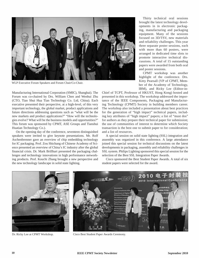
The Wafer Level Packaging (WLP) Executive Forum wasone of many highlights of this conference. Wafer Level ChipScalePackaging (WLCSP) is themost prominentWLPproducttoday.Industryanalysisreport indicates that inside the top three
high-endsmartphones, thirtytofiftypercentof thecomponentsare WLCSPs. New generations of CMOS Image Sensors (CIS)manufacturedinwaferlevelTSVprocess,arenowimplementedincellphonesandothermobileproducts.Themostrecentwaferlevelpackagingproductinhighvolumeproductionisthefan-outWLCSP.WaferlevelMEMsispositionedforavarietyofmarketimplementation.Thebasictechnologiesandmanufacturinginfra-structure(fan-in,fan-out,TSV,MEMs,CIS)areexpectedtoserveasbuildingblocksforheterogeneousand3Dintegration,and3DICarchitecturesfortheglobalmarket.TheWLPExecutiveForuminvitedagroupofseniortechnologistsandveteranbusinessexecu-tivesfromaroundtheglobetosharetheirknowledge,experienceandvision.ThesevenspeakersareWilliamChen(onbehalfofBillBottoms);JohnHunt(EngineeringDirector,ASEGroup);GlennDaves (PackagingDevDirector,FreescaleSemiconductor);BobForcier(President&CEO,FlipChipInternational);PeterElenius(Consultant, E&G Technology Partners); Jurgen Wolf (Group&ProjectManagerASSID,FraunhoferIZM);andHerbHuang(Director of Specialty Technology Development Semiconductor
ConferenceNews....
Prof.Bi(GeneralChair)withRolfAschenbrennerandWilliamChen.
GatheringatConferenceBanquet.
10 IEEE CPMT Society Newsletter September 2010
ManufacturingInternationalCorporation(SMIC),Shanghai).TheForum was co-chaired by Drs. William Chen and Wenhui Zhu(CTO, Tian Shui Hua Tian Technology Co. Ltd, China). Eachexecutivepresentedtheirperspective,atahigh-level,ofthisveryimportanttechnology,theglobalmarket,productapplicationsandfuturedirectionsaddressingquestions suchas“whatwillbe thenewmarketsandproductapplications?”“Howwillthetechnolo-giesevolve?Whatwillbe thebusinessmodelsandopportunities?”ThisforumwassponsoredbyCPMT,ASEGroupsandTianshuiHuatianTechnologyCo.).
Ontheopeningdayoftheconference,seventeendistinguishedspeakers were invited to give keynote presentations. Mr. RolfAschenbrennergaveanoverviewofchipembedding technologyforICpackaging.Prof.ZouShichangofChineseAcademyofSci-encepresentedanoverviewofChina’sICindustryaftertheglobalfinancialcrisis.Dr.MarkBrillhartpresentedthepackagingchal-lengesandtechnologyinnovationsinhighperformancenetwork-ingproducts.Prof.KouchiZhangbroughtanewperspectiveandthenewtechnologylandscapeinsolidstatelighting.
Thirty technical oral sessionsbroughtthelatesttechnologydevel-opments in in electronic packag-ing, manufacturing and packagingequipment. Many of the sessionsfocusedon3D/TSV, newmaterialsandreliabilitychallenges.Thisyearthreeseparatepostersessions,eachwith more than 60 posters, werearranged in dedicated time slots topromote interactive technical dis-cussions.A totalof15outstandingpaperswereawardedfrombothoralandpostersessions.
CPMT workshop was anotherhighlight of the conference. Drs.KittyPearsall(VPofCPMT,Mem-berof theAcademyofTechnology,IBM), and Ricky Lee (Editor-in-
ChiefofTCPT,ProfessorofHKUST,HongKong)hostedandpresentedinthisworkshop.Theworkshopaddressedtheimpor-tance of the IEEE Components, Packaging and Manufactur-ing Technology (CPMT) Society in building members career.Theworkshopalsoincludedapresentationaboutbestpracticesfor the generation of “high impact” technical papers, includ-ingkeyattributesof“highimpact”papers;alistof“mustdos”forauthorsastheypreparetheirtechnicalpaperforsubmission;theuseofcommunitiesofinteresttodeterminewhichSocietytransactionisthebestonetosubmitpapertoforconsideration;andalistofresources.
Aspecialsessiononsolidstatelighting(SSL)integrationandassembly was organized in this conference. A large attendancejoined thisspecialsessionfor technicaldiscussionson the latestdevelopmentsinpackaging,assemblyandreliabilitychallengesinSSLsystem.PhilipsLightingsponsoredthis specialsessionfortheselectionoftheBestSSLIntegrationPaperAwards.
CiscosponsoredtheBestStudentPaperAwards.Atotalofsixstudentpaperswereselectedfortheaward.
WLPExecutiveForumSpeakersandForumChair/Co-Chair.
Dr.RickyLeeatCPMTWorkshop. CiscoBestStudentPaperAwardsCeremony.

11September 2010 IEEE CPMT Society Newsletter
ESTC 2010 – a rESouNdINg SuCCESS!
ith 160 presentations, 4 poster sessions, a 3-day indus-try exhibition, workshops and short courses, the third
Electronics System Integration Technology Conference ESTC 2010 was truly an immersive experience for the almost 500 conference delegates. No matter what your background in micro system packaging, the conference had something for everyone. IEEE-CPMT, IMAPS Germany and Fraunhofer IZM as organiz-ers are particularly pleased that the conference participants, repre-senting 34 different countries, came from industry and academia in equal part and, based on the networking observed on the confer-ence floor and at the social events, it seems everyone went home with new contacts, insights and inspiration.
CPMT president and ESTC chair Rolf Aschenbrenner pointed out that a milestone was achieved in 2010 – ESTC is now undoubt-edly Europe’s premier packaging conference.
Among the many highlights of the conference the gala dinner at Meilenwerk stood out, with car fans and aesthetes alike marveling at classic cars from bygone eras. It was also a great chance to farewell one of the industry’s pioneers, Herbert Reichl, who received a spe-cial award for his long-term and significant contributions to micro system packaging. Jorma Kivilahti, who was to be honored with the IEEE Section 8 Award, had unfortunately been taken ill and Mervi Palasto from Aalto University accepted the award in his place.
Our congratulations go to the winners of the Best Paper Award (Yoichiro Kurita et. al. from Renesas Electronics Corporation) on Fan-Out Wafer-Level Packaging with Highly Flexible Design Capability and Best Poster Award (M. Bouchoucha et. al. from STMicroelectronics) on Through Silicon Via Polymer Filling for 3D-WLP Applications.
The organizers would like to thank all participants for ensuring ESTC 2010 was such a resounding success and look forward to what will surely be another standout ESTC in Amsterdam in 2012.
Panel Discussion with the Panel Members.
Plenary Hall during the Keynote Session.
The Conference Exhibition with Eric Beyne and Chris Bailey.
Opening Speech of the General Chair, Rolf Aschenbrenner.
W
12 IEEE CPMT Society Newsletter September 2010
IEEE CPMT SyMPOSIUM JAPAN (10TH VLSI PACKAGE WORKSHOP IN JAPAN)
IEEEVLSIPackageWorkshopinJapan”hasbeenheldeveryotheryearsince1992andreached the tenthanniversary thisyear.Basedonseveralconsiderations,thisWorkshophasbeen
transformedthisyearto“IEEECPMTSymposiumJapan”(ICSJ)bythejointeffortofIEEECPMTJapanChapterandtheorganiz-ingcommittee.ICSJintendstoprovideresearchersandengineerswhowishtoextendtheiractivitiesbeyondborderswithopportuni-tiestoexchangetechnicalknowledgeandperspective.
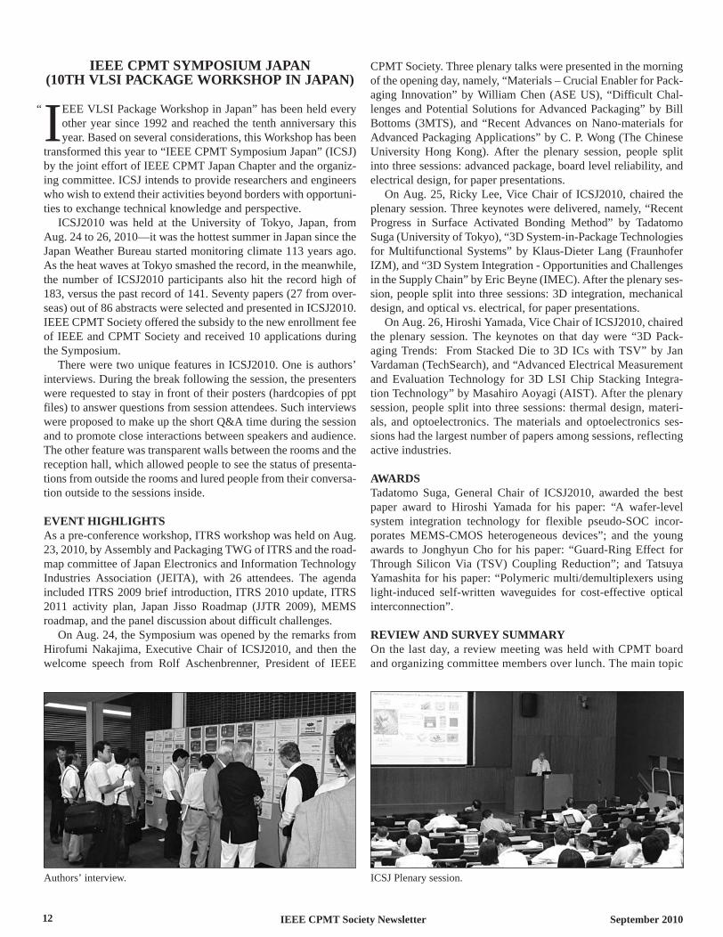
ICSJ2010 was held at the University of Tokyo, Japan, fromAug.24to26,2010—itwasthehottestsummerinJapansincetheJapanWeatherBureaustartedmonitoringclimate113yearsago.AstheheatwavesatTokyosmashedtherecord,inthemeanwhile,thenumberof ICSJ2010participantsalsohit the recordhighof183,versusthepastrecordof141.Seventypapers(27fromover-seas)outof86abstractswereselectedandpresentedinICSJ2010.IEEECPMTSocietyofferedthesubsidytothenewenrollmentfeeofIEEEandCPMTSocietyandreceived10applicationsduringtheSymposium.
ThereweretwouniquefeaturesinICSJ2010.Oneisauthors’interviews.Duringthebreakfollowingthesession,thepresenterswererequestedtostayinfrontoftheirposters(hardcopiesofpptfiles)toanswerquestionsfromsessionattendees.SuchinterviewswereproposedtomakeuptheshortQ&Atimeduringthesessionandtopromotecloseinteractionsbetweenspeakersandaudience.Theotherfeaturewastransparentwallsbetweentheroomsandthereceptionhall,whichallowedpeopletoseethestatusofpresenta-tionsfromoutsidetheroomsandluredpeoplefromtheirconversa-tionoutsidetothesessionsinside.
EVENT HIGHLIGHTSAsapre-conferenceworkshop,ITRSworkshopwasheldonAug.23,2010,byAssemblyandPackagingTWGofITRSandtheroad-mapcommitteeofJapanElectronicsandInformationTechnologyIndustries Association (JEITA), with 26 attendees. The agendaincludedITRS2009briefintroduction,ITRS2010update,ITRS2011 activity plan, Japan Jisso Roadmap (JJTR 2009), MEMSroadmap,andthepaneldiscussionaboutdifficultchallenges.
OnAug.24,theSymposiumwasopenedbytheremarksfromHirofumiNakajima,ExecutiveChairof ICSJ2010, and then thewelcome speech from Rolf Aschenbrenner, President of IEEE
CPMTSociety.Threeplenarytalkswerepresentedinthemorningoftheopeningday,namely,“Materials–CrucialEnablerforPack-aging Innovation”byWilliamChen (ASEUS), “DifficultChal-lengesandPotentialSolutionsforAdvancedPackaging”byBillBottoms (3MTS), and “RecentAdvancesonNano-materials forAdvancedPackagingApplications”byC.P.Wong(TheChineseUniversity Hong Kong). After the plenary session, people splitintothreesessions:advancedpackage,boardlevelreliability,andelectricaldesign,forpaperpresentations.
OnAug.25,RickyLee,ViceChairofICSJ2010,chairedtheplenarysession.Threekeynotesweredelivered,namely,“RecentProgress in Surface Activated Bonding Method” by TadatomoSuga(UniversityofTokyo),“3DSystem-in-PackageTechnologiesforMultifunctionalSystems”byKlaus-DieterLang (FraunhoferIZM),and“3DSystemIntegration-OpportunitiesandChallengesintheSupplyChain”byEricBeyne(IMEC).Aftertheplenaryses-sion,peoplesplitintothreesessions:3Dintegration,mechanicaldesign,andopticalvs.electrical,forpaperpresentations.
OnAug.26,HiroshiYamada,ViceChairofICSJ2010,chairedthe plenary session.The keynotes on that daywere “3DPack-agingTrends: FromStackedDie to3DICswithTSV”byJanVardaman(TechSearch),and“AdvancedElectricalMeasurementand Evaluation Technology for 3D LSI Chip Stacking Integra-tionTechnology”byMasahiroAoyagi(AIST).Aftertheplenarysession,peoplesplitintothreesessions:thermaldesign,materi-als, andoptoelectronics.Thematerials andoptoelectronics ses-sionshadthelargestnumberofpapersamongsessions,reflectingactiveindustries.
AWARDSTadatomo Suga, General Chair of ICSJ2010, awarded the bestpaper award to Hiroshi Yamada for his paper: “A wafer-levelsystem integration technology for flexible pseudo-SOC incor-porates MEMS-CMOS heterogeneous devices”; and the youngawards to JonghyunCho forhispaper: “Guard-RingEffect forThrough Silicon Via (TSV) Coupling Reduction”; and TatsuyaYamashitaforhispaper:“Polymericmulti/demultiplexersusinglight-induced self-written waveguides for cost-effective opticalinterconnection”.
REVIEW AND SURVEy SUMMARyOnthelastday,areviewmeetingwasheldwithCPMTboardandorganizingcommitteemembersoverlunch.Themaintopic
“
Authors’interview. ICSJPlenarysession.

13September 2010 IEEE CPMT Society Newsletter
of this discussion was the recommendation of transformingICSJfromabiennialeventtoanannualevent.TherehavebeentwobiennialeventsinJapansponsoredbyIEEECPMTSociety:VLSI Package Workshop and System Packaging Workshop.The recommendation was to merge these two biennial eventsto make one annual event, which shall accelerate the growthofbothevents.aconsensuswasreachedthatKishioYokouchi,Co-chair of IEEE CPMT Japan Chapter, would look into thepossibilityofthemergeroftwoevents,afterresolvingthespon-
sorshipissueofIEEEComputerSocietytotheSystemPackag-ingWorkshop.
Attendee’ssurveyindicatedcompletesatisfactiontotheauthors’interviewsystem,whichenabledmuchmoreinteractionsandinspi-ration between speakers and session attendees. Forty percent ofparticipantsmarked“excellent”ontheinterviewsand30%onthereception,whichwasboostedupbythehigh-spirittalksdeliveredbythechairsandinvitedguests.Furthermore,highqualityplenarykeynoteswereanothermeritcommendedbyICSJ2010attendees.
IEEE Semiconductor Wafer Test WorkshopJune6to9,2010atRanchoBernardoInn,SanDiego,CA
SubmittedbyJerryBroz,Ph.D.,GeneralChairofIEEESWTestWorkshopandIEEESeniorMember.
The20thAnnualIEEESemiconductorWaferTestWorkshop(SW Test) was held at the Rancho Bernardo Inn in SanDiego,CA,fromJune6to9,2010.Thisannualworkshop
bringstogethertechnologists,engineers,andmanagersaswellassales and marketing professionals involved with all aspects ofprobetechnologyandwaferleveltesting.SWTest2010consistedofatechnicalprogram,supplierexhibits(whichARENOTopenduringthetechnicalsessions),andaCasinoRoyaleSocialEventaswellasplentyoftimeforinformalinteractionandnetworkingwithcolleagues.TotalconferenceandEXPOattendancewas270with approximately 23% international attendees representing 14countries.Thisyear,SWTestalsohadagoodmixofend-users(~28%)andsuppliers(~72%)inattendance.
After thewelcome receptiononSundayevening, JerryBroz,Ph.D., SW Test General Chair, gave a short, “Probe Year InReview”duringwhichhepaidtributetothreekeyprobetechnolo-giststhatpassedawayduringthe12-months–FrankPietzschmann(Qimonda AG and SW Test Committee Member), Brett Crump(MicronTechnologyandSWTestTechnicalChair),andBillMann(founderofSWTestWorkshop).Dr.BrozalsoannouncedhisworkwiththeIEEEFoundationtoestablishaWilliam R. Mann Memo-rial Student Grant Fund.
Dr.BrozreviewedSIAstatisticswhichhighlightedexactlyhowbad2009was for the semiconductor industry, e.g.,FAButiliza-tionfellbelow60%duringthefirstquarter,etc.Onlythreeofthetop twenty semiconductorcompanies,Samsung,QualcommandMediaTek,showedanyrevenuegrowth.Interestingly,QualcommandMediaTek(whichshowedgrowthof+21%)areFAB-lesssemi-conductorcompanies.Notsurprisingly,thebadyearwasreflectedintheVLSIResearchprobecardmarketoverviewreleasedinMay.Totalprobecardrevenuewasdown~29%(from~$1.0Bin2008to~$700Min2009).Thetopthreeprobecardsuppliersremainedunchanged–(1)FormFactor;(2)MicronicsJapan(MJC),and(3)JapanElectronicMaterials (JEM);however, all threecompaniesexperiencedreducedrevenue.Microprobe,Inc.,movedfrom9thto5thandwastheonlycompanyintheTop10thatshowedincreasedrevenue.
DeanFreeman,VPofResearchatGartnerResearch,madetheKeynotePresentationentitled,“What’s Going to Rock Your World
– Or At Least Push Your Probes”.Mr.Freemanfocusedonthree“hot”technologiesthatGartnerResearchbelieveswilldrivesemi-conductor demand – (1) Cloud Computing, (2) Green Tech/IT,and(3)SocialComputing.ForCloudComputing,Gartnerexpectsaninfrastructurewherethe“dumb”terminalswillaccessamorepowerfulcentralizedcomputingresource.DemandsforrenewableenergywillcontinuetodriveGreenTech/ITwiththeapplicationsforenergygeneration,reducedconsumption,andformsofenergystorage. Gartner also predicts that Social Computing demands,suchastwitter®,Facebook®,etc.,ofthe“connected”generationwillfurtheraccelerateanddriveadoptionofmobiledeviceswithfurtheraccesstoanmore“real-time”,yetsecure,networkinfra-structure.
Mr.FreemandiscussedthatchasingMoore’sLawwillrequireeachIDMtohave“extremelydeeppockets”. In fact, such tech-nology development might only be attained by Intel, Samsung,Toshiba, and large foundries such as TSMC, UMC, or Global-Foundries.Thetransitionto450-mmwaferswillbea“large”partofthefutureandhasbecomeaconstructivedialogsuchthatpro-totypeFABsmightbetoolingupin2016to2017andproduction-levelFABsreadyasearlyas2018to2020.Finally,Deanshowedthat the semiconductor industry seems to be back on track andexpects~27%growthfor2010.Itispossiblethatthesemi-marketcould finally cross the$300B threshold in2011. ThecompleteversionofDeanFreeman’skeynotepresentation is available fordownloadontheSWTestwebsite(http://www.swtest.org).
OnMondaymorningDr.JerryBrozwelcomedattendeestothe20thAnnual SWTestWorkshop and the technical programhadpresentationscoveringeveryfacetof thewafer testprocessfromDevelopments for Improved Scribeline Probing to Large Area
Networking.
14 IEEE CPMT Society Newsletter September 2010
Array Probing.IndividualhighlightsfromtheprogramincludedanoverviewofthebenefitsofflipchipwafersortusingMEMsmulti-sitecapabilitybyLoWeeTick(GlobalFoundries).JohnHite(TexasInstruments)discussedstandardizationofwafersocketspring-pinprobecardsforacosteffectiveapproachtochipscalepackagetest-ing.RayRobertazzi(IBMResearch)outlinedanapproachfornewdirections inparametricanddefect structure testing.The taskofaddressingoperatingchallengesneeded for fullwafercontactorsunder demanding wafer sort conditions was presented by KeithBreinlinger,Ph.D.,fromFormFactor.Theimportanceofacorre-lated probecard analysis and probemark inspection methods foroptimizingtestcellperformancewasdetailedbyReyRincon(Fre-escale)andJeffGreenberg(RudolphTechnologies).Assessingcur-rentcarryingcapacityusingastandardandconsistentmethodologywasdetailedbyMattZeman,Ph.D.,(IntelCorporation).TechnicalhurdlesexperiencedforoptimizationtoreducecostofownershipwerereviewedbyThomasLogue(Seagate–Ireland).RyanSatromandJasonMroczkowski(Multitest |ECT)andGertHohenwarter(GateWaveNorthern)discussedtheimportanceofsignalintegritywithinchallengingwafertestenvironment.Overall, thetechnicalprogramhad27podiumpresentationswith60% fromsuppliers,15% from semiconductor manufacturers, and 25% collaborativepresentationsfrombothmanufacturersandsuppliers.
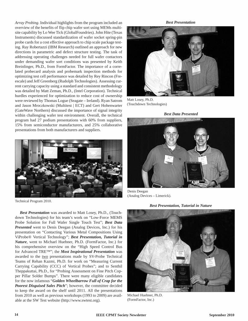
BestPresentationwasawardedtoMattLosey,Ph.D.,(Touch-downTechnologies)forhis team’sworkon“Low-ForceMEMSProbe Solution for Full Wafer Single Touch Test”; Best DataPresentedwent toDenisDeegan (AnalogDevices, Inc.) forhispresentation on “Contacting Various Metal Compositions UsingViProbe® Vertical Technology”; Best Presentation, Tutorial inNature,went toMichaelHuebner, Ph.D. (FormFactor, Inc.) forhis comprehensive overview on the “High Speed Control BusforAdvancedTRE™”;theMostInspirationalPresentationwasawarded to the two presentations made by SV-Probe TechnicalTeamsofRehanKazmi,Ph.D. forworkon“MeasuringCurrentCarrying Capability (CCC) of Vertical Probes”; and to SenthilTheppakuttai,Ph.D.,for“ProbingAssessmentonFinePitchCop-per Pillar Solder Bumps”. There were many eligible candidatesforthenowinfamous“GoldenWheelbarrowFullofCrapforthePoorestDisguisedSalesPitch”;however,thecommitteedecidedtokeep the awardon the shelf until 2011.All thepresentationsfrom2010aswellaspreviousworkshops(1993to2009)areavail-ableattheSWTestwebsite(http://www.swtest.org).
TechnicalProgram2010.
BestPresentation
MattLosey,Ph.D.(TouchdownTechnologies)
BestDataPresented
DenisDeegan(AnalogDevices–Limerick).
BestPresentation,TutorialinNature
MichaelHuebner,Ph.D.(FormFactor,Inc.)

15September 2010 IEEE CPMT Society Newsletter
SW Test EXPO had 28 industry exhibitors and four Corpo-rateSupporters(AcmeTechnology,Inc.,AdvancedProbingSys-tems,InternationalTestSolutions,andJEMAmerica).DuringtheEXPO,allaspectsofthewafersortindustryandassociatedinfra-structuresupplierswererepresentedwithmostprobecardvendors,majorproberequipmentmanufacturers,probecardanalyzerandprobe process metrology companies, companies specializing in
probe card cleaning,micro-pogo pin suppliers, and a variety ofotherproberelatedserviceproviders.
The 21st Annual IEEE SW Test Workshop and Tech EXPOwillbeheldonJune 12 to 15, 2011attheRanchoBernardoInn,San Diego, CA (http://www.ranchobernardoinn.com). Abstractsubmissionforpodiumandposterpresentationswillbeopenstart-ingJanuary1,2011.
MostInspirationalPresentation
RehanKazmi,Ph.D.&SenthilTheppakuttai,Ph.D.(SV-Probe,Inc.) TechnologyEXPO2010.
Put your Technology Leadership in Writing!
Publish in our IEEE Transactions
Figures in full color; worldwide access to results.
For more details: www.cpmt.org/trans/
Contribute to Fall Newsletter Issue
IEEE CPMT Society News
Send your news articles to the editor at [email protected]
Access Papers from CPMT Conferences(ECTC, ESTC, EPTC etc):
Visit ieeexplore.ieee.org and download them

16 IEEE CPMT Society Newsletter September 2010
IEEE Components, Packaging and ManufacturingTechnology SocietyMarsha Tickman, Executive Director445 Hoes LanePiscataway, NJ 08854 USA
Name: 5thInt’lMicrosystems,Packaging,AssemblyandCircuitsTechnology(IMPACT2010)
Dates: October20–22,2010Location: Taipei,TaiwanE-mail: [email protected]: http://www.impact.org.tw/2010/General/
Name: 19thIEEEConferenceonElectricalPerformanceofElectronicPackaging&Systems(EPEPS2010)
Dates: October24–27,2010Location: Austin,TX,USAContact: KellySuttonE-mail: [email protected]
Name: 4thInternationalConferenceon3DSystemIntegration(3DIC2010)
Dates: November16–18,2010Location: Munich,GermanyContact: PeterRamm,FraunhoferE-mail: [email protected]: http://www.3dic-conf.org/
Name: 34thInternationalElectronicsManufacturingTechnologyConference(IEMT)
Dates: Nov.30–Dec.2,2010Location: Melaka,MalaysiaContact: TracyOwInfineonE-mail: [email protected]: http://ewh.ieee.org/r10/malaysia/cpmt/iemt.htm
Name: ElectricalDesignofAdvancedPackage&SystemsSymposium(EDAPS)
Dates: Dec.7–9,2010Location: SingaporeContact: Dr.Er-PingLi,A*STARE-mail: [email protected]: http://www.edaps2010.org/
Name: 12thElectronicsPackagingTechnologyConference(EPTC2010)
Dates: December8–10,2010Location: SingaporeE-mail: [email protected]: http://www.eptc-ieee.net/
Name: 3rdInternationalConferenceonThermalIssuesinEmergingTechnologies,TheoryandApplications(ThETA3)
Dates: December19–22,2010Location: Cairo,EgyptContact: Mohamed-NabilSabryE-mail: [email protected]: http://www.thetaconf.org/
Name: 27thInt’lSemiconductorThermalModeling,MeasurementandManagementSymposium(SEMI-THERM)
Dates: March20–24,2011Location: SanJose,CAUSAContact: TomTarterE-mail: [email protected]: http://www.semi-therm.org/
UpcomingCPMTSocietyConferences....