data sheet june 13, 2006 - futureelectronics.com electronics/dg409dyz-t.pdf · 3a da s4a v+ s1b s3b...
TRANSCRIPT
1
®
DG408, DG409FN3283.8Data Sheet June 13, 2006
Single 8-Channel/Differential 4-Channel, CMOS Analog MultiplexersThe DG408 Single 8-Channel, and DG409 Differential 4-Channel monolithic CMOS analog multiplexers are drop-in replacements for the popular DG508A and DG509A series devices. They each include an array of eight analog switches, a TTL/CMOS compatible digital decode circuit for channel selection, a voltage reference for logic thresholds and an ENABLE input for device selection when several multiplexers are present.
The DG408 and DG409 feature lower signal ON resistance (<100Ω) and faster switch transition time (tTRANS < 250ns) compared to the DG508A or DG509A. Charge injection has been reduced, simplifying sample and hold applications. The improvements in the DG408 series are made possible by using a high-voltage silicon-gate process. An epitaxial layer prevents the latch-up associated with older CMOS technologies. Power supplies may be single-ended from +5V to +34V, or split from ±5V to ±20V.
The analog switches are bilateral, equally matched for AC or bidirectional signals. The ON resistance variation with analog signals is quite low over a ±5V analog input range.
Features• ON Resistance (Max, 25°C). . . . . . . . . . . . . . . . . . . 100Ω
• Low Power Consumption (PD) . . . . . . . . . . . . . . . <11mW
• Fast Switching Action- tTRANS . . . . . . . . . . . . . . . . . . . . . . . . . . . . . . . . <250ns- tON/OFF(EN) . . . . . . . . . . . . . . . . . . . . . . . . . . . . <150ns
• Low Charge Injection
• Upgrade from DG508A/DG509A
• TTL, CMOS Compatible
• Single or Split Supply Operation
• Pb-Free Plus Anneal Available (RoHS Compliant)
Applications• Data Acquisition Systems
• Audio Switching Systems
• Automatic Testers
• Hi-Rel Systems
• Sample and Hold Circuits
• Communication Systems
• Analog Selector Switch
Ordering InformationPART
NUMBERPART
MARKINGTEMP.
RANGE (°C) PACKAGEPKG.
DWG. #
DG408DJ DG408DJ -40 to 85 16 Ld PDIP E16.3
DG408DJZ (Note) DG408DJZ -40 to 85 16 Ld PDIP** (Pb-free) E16.3
DG408DY* DG408DY -40 to 85 16 Ld SOIC M16.15
DG408DYZ* (Note) DG408DYZ -40 to 85 16 Ld SOIC (Pb-free) M16.15
DG408DVZ* (Note) DG408DVZ -40 to 85 16 Ld TSSOP (Pb-free) M16.173
DG409DJ DG409DJ -40 to 85 16 Ld PDIP E16.3
DG409DJZ (Note) DG409DJZ -40 to 85 16 Ld PDIP** (Pb-free) E16.3
DG409DY* DG409DY -40 to 85 16 Ld SOIC M16.15
DG409DYZ* (Note) DG409DYZ -40 to 85 16 Ld SOIC (Pb-free) M16.15
DG409DVZ* (Note) DG409DVZ -40 to 85 16 Ld TSSOP (Pb-free) M16.173
*Add “-T” suffix for tape and reel.**Pb-free PDIPs can be used for through hole wave solder processing only. They are not intended for use in Reflow solder processing applications.NOTE: Intersil Pb-free plus anneal products employ special Pb-free material sets; molding compounds/die attach materials and 100% matte tin plate termination finish, which are RoHS compliant and compatible with both SnPb and Pb-free soldering operations. Intersil Pb-free products are MSL classified at Pb-free peak reflow temperatures that meet or exceed the Pb-free requirements of IPC/JEDEC J STD-020.
CAUTION: These devices are sensitive to electrostatic discharge; follow proper IC Handling Procedures.1-888-INTERSIL or 1-888-468-3774 | Intersil (and design) is a registered trademark of Intersil Americas Inc.
Copyright Intersil Americas Inc. 1993, 1994, 1997, 1999, 2004, 2006. All Rights ReservedAll other trademarks mentioned are the property of their respective owners.

DG408, DG409
PinoutsDG408 (PDIP, SOIC, TSSOP)
TOP VIEWDG409 (PDIP, SOIC, TSSOP)
TOP VIEW
Functional Block DiagramsDG408 DG409
14
15
16
9
13
12
11
10
1
2
3
4
5
7
6
8
A0
EN
V-
S1
S2
S3
D
S4
A1
GND
V+
S5
S6
S7
S8
A2
14
15
16
9
13
12
11
10
1
2
3
4
5
7
6
8
A0
EN
V-
S1A
S2A
S3A
DA
S4A
A1
V+
S1B
S3B
S4B
DB
GND
S2B
TRUTH TABLE DG408
A2 A1 A0 EN ON SWITCH
X X X 0 NONE
0 0 0 1 1
0 0 1 1 2
0 1 0 1 3
0 1 1 1 4
1 0 0 1 5
1 0 1 1 6
1 1 0 1 7
1 1 1 1 8
DECODER/DRIVER
D
LEVELSHIFT
†† ††
5VREF
DIGITALINPUTPROTECTION
†
S1
S2
S8
A0 A1 A2 EN
TRUTH TABLE DG409
A1 A0 EN ON SWITCH
X X 0 NONE
0 0 1 1
0 1 1 2
1 0 1 3
1 1 1 4
NOTES:1. VAH Logic “1” ≥2.4V.2. VAL Logic “0” ≤0.8V.
DECODER/DRIVER
DA
LEVELSHIFT
†††
5VREF
DIGITALINPUTPROTECTION
†
S1A
S4A
S1B
A0 A1 EN
DB
S4B
2 FN3283.8June 13, 2006

DG408, DG409
Pin Descriptions - (DG408)PIN SYMBOL DESCRIPTION
1 A0 Logic Decode Input (Bit 0, LSB)
2 EN Enable Input
3 V- Negative Power Supply Terminal
4 S1 Source (Input) for Channel 1
5 S2 Source (Input) for Channel 2
6 S3 Source (Input) for Channel 3
7 S4 Source (Input) for Channel 4
8 D Drain (Output)
9 S8 Source (Input) for Channel 8
10 S7 Source (Input) for Channel 7
11 S6 Source (Input) for Channel 6
12 S5 Source (Input) for Channel 5
13 V+ Positive Power Supply Terminal (Substrate)
14 GND Ground Terminal (Logic Common)
15 A2 Logic Decode Input (Bit 2, MSB)
16 A1 Logic Decode Input (Bit 1)
Pin Descriptions - (DG409)PIN SYMBOL DESCRIPTION
1 A0 Logic Decode Input (Bit 0, LSB)
2 EN Enable Input
3 V- Negative Power Supply Terminal
4 S1A Source (Input) for Channel 1a
5 S2A Source (Input) for Channel 2a
6 S3A Source (Input) for Channel 3a
7 S4A Source (Input) for Channel 4a
8 DA Drain a (Output a)
9 DB Drain b (Output b)
10 S4B Source (Input) for Channel 4b
11 S3B Source (Input) for Channel 3b
12 S2B Source (Input) for Channel 2b
13 S1B Source (Input) for Channel 1b
14 V+ Positive Power Supply Terminal
15 GND Ground Terminal (Logic Common)
16 A1 Logic Decode Input (Bit 1, MSB)
3 FN3283.8June 13, 2006

DG408, DG409
Absolute Maximum Ratings Thermal InformationV+ to V- . . . . . . . . . . . . . . . . . . . . . . . . . . . . . . . . . . . . . . . . . . 44.0VGND to V-. . . . . . . . . . . . . . . . . . . . . . . . . . . . . . . . . . . . . . . . . . .25VDigital Inputs, VS, VD (Note 3). . . . . .(V-) -2V to (V+) + 2V or 20mA,
Whichever Occurs FirstContinuous Current (Any Terminal) . . . . . . . . . . . . . . . . . . . . . 30mAPeak Current, S or D (Pulsed 1ms, 10% Duty Cycle Max) . . 100mA
Operating ConditionsTemperature Range . . . . . . . . . . . . . . . . . . . . . . . . . . -40°C to 85°C
Thermal Resistance (Typical, Note 4) θJA (°C/W)PDIP Package . . . . . . . . . . . . . . . . . . . . . . . . . . . . . 90SOIC Package . . . . . . . . . . . . . . . . . . . . . . . . . . . . . 110TSSOP Package . . . . . . . . . . . . . . . . . . . . . . . . . . . 150
Maximum Junction Temperature . . . . . . . . . . . . . . . . . . . . . . . 150°CMaximum Storage Temperature Range . . . . . . . . . . -65°C to 125°CMaximum Lead Temperature (Soldering 10s) . . . . . . . . . . . . . 300°C
(SOIC and TSSOP - Lead Tips Only)
CAUTION: Stresses above those listed in “Absolute Maximum Ratings” may cause permanent damage to the device. This is a stress only rating and operation of thedevice at these or any other conditions above those indicated in the operational sections of this specification is not implied.
NOTES:3. Signals on SX, DX, EN or AX exceeding V+ or V- are clamped by internal diodes. Limit diode current to maximum current ratings.4. θJA is measured with the component mounted on an evaluation PC board in free air.
Electrical Specifications Test Conditions: V+ = +15V, V- = -15V, VAL = 0.8V, VAH = 2.4V, Unless Otherwise Specified
PARAMETER TEST CONDITIONS TEMP (°C)(NOTE 5)
MIN(NOTE 6)
TYP(NOTE 5)
MAX UNITS
DYNAMIC CHARACTERISTICS
Transition Time, tTRANS (See Figure 1) Full - 160 250 ns
Break-Before-Make Interval, tOPEN (See Figure 3) 25 10 - - ns
Enable Turn-ON Time, tON(EN) (See Figure 2) 25 - 115 150 ns
Full - - 225 ns
Enable Turn-OFF Time, tOFF(EN) (See Figure 2) Full - 105 150 ns
Charge Injection, Q CL = 10nF, VS = 0V 25 - 20 - pC
OFF Isolation VEN = 0V, RL = 1kΩ,f = 100kHz (Note 9)
25 - -75 - dB
Logic Input Capacitance, CIN f = 1MHz 25 - 8 - pF
Source OFF Capacitance, CS(OFF) VEN = 0V, VS = 0V,f = 1MHz
25 - 3 - pF
Drain OFF Capacitance, CD(OFF) VEN = 0V, VD = 0V,f = 1MHzDG408 25 - 26 - pF
DG409 25 - 14 - pF
Drain ON Capacitance, CD(ON) VEN = 3V, VD = 0V,f = 1MHz, VA = 0V or 3VDG408 25 - 37 - pF
DG409 25 - 25 - pF
DIGITAL INPUT CHARACTERISTICS
Logic Input Current,Input Voltage High, IAH
VA = 2.4V, 15V Full -10 - 10 µA
Logic Input Current,Input Voltage Low, IAL
VEN = 0V, 2.4V,VA = 0V
Full -10 - 10 µA
ANALOG SWITCH CHARACTERISTICS
Analog Signal Range, VANALOG Full -15 - 15 V
Drain-Source ON Resistance,rDS(ON)
VD = ±10V, IS = -10mA(Note 7)
25 - 40 100 Ω
Full - - 125 Ω
rDS(ON) Matching Between Channels, ∆rDS(ON)
VD = 10V, -10V (Note 8) 25 - - 15 Ω
Source OFF Leakage Current, IS(OFF) VEN = 0V, VS = ±10V,VD = +10V
25 -0.5 - 0.5 nA
Full -5 - 5 nA
4 FN3283.8June 13, 2006

DG408, DG409
Drain OFF Leakage Current, ID(OFF) VEN = 0V, VD = ±10V,VS = +10VDG408 25 -1 - 1 nA
Full -20 - 20 nA
DG409 25 -1 - 1 nA
Full -10 - 10 nA
Drain ON Leakage Current, ID(ON) VS = VD = ±10V (Note 7)DG408 25 -1 - 1 nA
Full -20 - 20 nA
DG409 25 -1 - 1 nA
Full -10 - 10 nA
POWER SUPPLY CHARACTERISTICS
Positive Supply Current, I+ VEN = 0V, VA = 0V (Standby) Full - 10 75 µA
Negative Supply Current, I- Full -75 1 - µA
Positive Supply Current, I+ VEN = 2.4V, VA = 0V(Enabled)
25 - 0.2 0.5 mA
Full - - 2 mA
Negative Supply Current, I- Full -500 - - µA
Electrical Specifications Test Conditions: V+ = +15V, V- = -15V, VAL = 0.8V, VAH = 2.4V, Unless Otherwise Specified (Continued)
PARAMETER TEST CONDITIONS TEMP (°C)(NOTE 5)
MIN(NOTE 6)
TYP(NOTE 5)
MAX UNITS
Electrical Specifications Single Supply Test Conditions: V+ = 12V, V- = 0V, VAL = 0.8V, VAH = 2.4V, Unless Otherwise Specified
PARAMETERTEST
CONDITION TEMP (°C)(NOTE 5)
MIN(NOTE 6)
TYP(NOTE 5)
MAX UNITS
DYNAMIC CHARACTERISTICS
Switching Time of Multiplexer, tTRANS VS1 = 8V, VS8 = 0V, VIN = 2.4V 25 - 180 - ns
Enable Turn-ON Time, tON(EN) VINH = 2.4V, VINL = 0V,VS1 = 5V
25 - 180 - ns
Enable Turn-OFF Time, tOFF(EN) 25 - 120 - ns
Charge Injection, Q CL = 10nF, VGEN = 0V,RGEN = 0Ω
25 - 5 - pC
ANALOG SWITCH CHARACTERISTICS
Analog Signal Range, VANALOG Full 0 - 12 V
Drain-Source ON-Resistance,rDS(ON)
VD = 3V, 10V, IS = -1mA(Note 7)
25 - 90 - Ω
NOTES:5. The algebraic convention whereby the most negative value is a minimum and the most positive a maximum, is used in this data sheet.6. Typical values are for DESIGN AID ONLY, not guaranteed nor production tested.7. Sequence each switch ON.8. ∆rDS(ON) = rDS(ON) (Max) - rDS(ON) (Min).9. Worst case isolation occurs on channel 4 due to proximity to the drain pin.
5 FN3283.8June 13, 2006

DG408, DG409
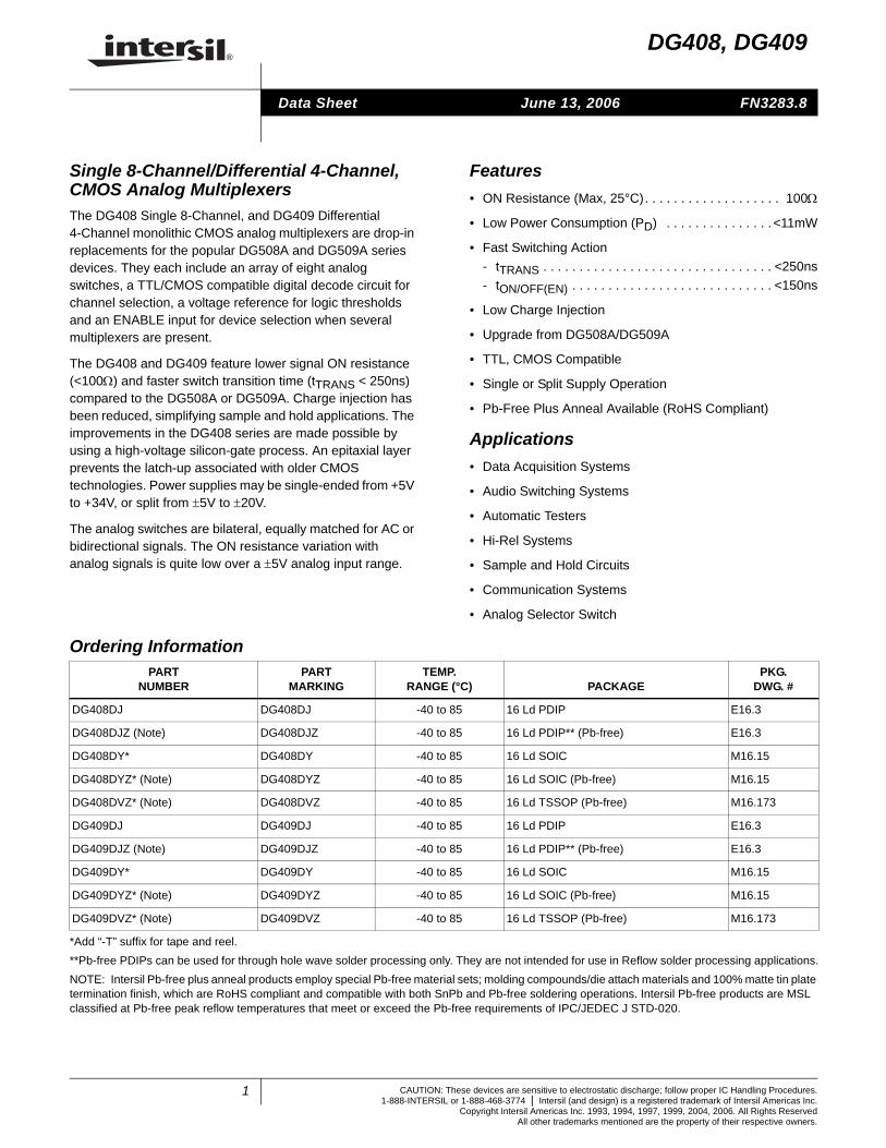
Test Circuits and Waveforms
FIGURE 1A. DG408 TEST CIRCUIT FIGURE 1B. DG409 TEST CIRCUIT
FIGURE 1C. MEASUREMENT POINTS
FIGURE 1. TRANSITION TIME
FIGURE 2A. DG408 TEST CIRCUIT FIGURE 2B. DG409 TEST CIRCUIT
FIGURE 2C. MEASUREMENT POINTS
FIGURE 2. ENABLE SWITCHING TIMES
ENA0
DG408
GND
A1
A2
S1S2 - S7
S8
DV-
V+
10V
±10V
SWITCHOUTPUT
VO
35pF300Ω50Ω
+15V+2.4V
-15V
LOGICINPUT
±
EN
DG409
GND
A0
A1
S1BS1A - S4A, DA
S4B
DBV-
V+
10V
±10V
SWITCHOUTPUT
VO
35pF300Ω50Ω
+15V+2.4V
-15V
LOGICINPUT
±
LOGICINPUT
SWITCHOUTPUT
VO
3V
VS1S1 ON
50%
tr < 20nstf < 20ns
tTRANS
50%0V
0V
VS8
tTRANSS8 ON
0.8 VS8
0.8 VS1
EN
A0 DG408
GND
A1A2
S1
S2 - S8
DV-
V+-5V
SWITCHOUTPUT
VO
35pF300Ω50Ω
+15V
-15V
LOGICINPUT VIN
EN
A0 DG409
GND
A1
S1B
S1A - S4A
DBV-
V+-5V
SWITCHOUTPUT
Vo
35pF300Ω50Ω
+15V
-15V
LOGICINPUT S2B - S4B, DAVIN
LOGICINPUT
SWITCHOUTPUT
VO
3V
VO
50%
tr < 20nstf < 20ns
tON(EN)
0V50%
tOFF(EN)
0.9 VO
0V
VIN
6 FN3283.8June 13, 2006
DG408, DG409
FIGURE 3A. TEST CIRCUIT FIGURE 3B. MEASUREMENT POINTS
FIGURE 3. BREAK-BEFORE-MAKE INTERVAL
FIGURE 4A. TEST CIRCUIT FIGURE 4B. MEASUREMENT POINTS
FIGURE 4. CHARGE INJECTION
FIGURE 5. OFF ISOLATION FIGURE 6. CROSSTALK
Test Circuits and Waveforms (Continued)
ENA0 DG408
GND
A1
A2
ALL S AND DA
D, DBV-
V++5V (VS)
SWITCHOUTPUT
VO
35pF300Ω50Ω
+15V
+2.4V
-15V
LOGICINPUT
DG409
LOGICINPUT
SWITCHOUTPUT
VO
3V
VS
80%
tr < 20nstf < 20ns
tOPEN
0V
0V
80%
SX
A0
GND
A1
EN
D
V-
V+VO
CL
+15V
-15V
A2
10nFVGEN CHANNEL
SELECT
RGEN
LOGIC INPUT
LOGICINPUT
SWITCHOUTPUT ∆VO
3V
ON OFF
0V
∆VO IS THE MEASURED VOLTAGE DUETO CHARGE TRANSFER ERROR, QQ = CL x ∆VO
SX
A2
GND
A1
EN
D
V-
V+
VO
+15V
-15V
A0SIGNAL
GENERATOR
VIN
0V
1kΩ
ANALYZER
||
S8
OFF ISOLATION 20 LogVOUT
VIN-----------------=
SX
A2
GND
A1
EN
D
V-
V+
VO
+15V
-15V
A0SIGNAL
GENERATOR
VIN
5V
1kΩ
ANALYZER
||
S8
CROSSTALK 20 LogVOUT
VIN-----------------=
S1
1kΩ
7 FN3283.8June 13, 2006

DG408, DG409
Typical ApplicationsOvervoltage ProtectionA very convenient form of overvoltage protection consists of adding two small signal diodes (1N4148, 1N914 type) in series with the supply pins (see Figure 9). This arrangement effectively blocks the flow of reverse currents. It also floats the supply pin above or below the normal V+ or V- value. In this case the overvoltage signal actually becomes the power supply of the IC. From the point of view of the chip, nothing has changed, as long as the difference V+ - (V-) doesn’t exceed 44V. The addition of these diodes will reduce the analog signal range to 1V below V+ and 1V above V-, but it preserves the low channel resistance and low leakage characteristics.
Typical application information is for Design Aid Only, not guaranteed and not subject to production testing.
FIGURE 7. INSERTION LOSS FIGURE 8. SOURCE/DRAIN CAPACITANCES
Test Circuits and Waveforms (Continued)
A2
GND
A1
EN
D
V-
V+
VO
+15V
-15V
A0
SIGNALGENERATOR
VIN
5V
RL
ANALYZER
INSERTION LOSS 20 LogVOUT
VIN-----------------=
S1
IMPEDANCEANALYZER
A2
GND
A1
EN
V-
V+
+15V
-15V
A0
CHANNELSELECT
3V OR 0V
S8
S1||
D
1N4148
1N4148
DG408
V-
VG
SX
V+
D
FIGURE 9. OVERVOLTAGE PROTECTION USING BLOCKING DIODES
8 FN3283.8June 13, 2006

DG408, DG409
Typical Performance Curves
FIGURE 10. INPUT LOGIC CURRENT vs LOGIC INPUT VOLTAGE
FIGURE 11. SOURCE/DRAIN CAPACITANCE vs ANALOG VOLTAGE (SINGLE 12V SUPPLY)
FIGURE 12. SOURCE/DRAIN CAPACITANCE vs ANALOG VOLTAGE
FIGURE 13. LOGIC INPUT CURRENT vs TEMPERATURE
FIGURE 14. DRAIN LEAKAGE CURRENT vs SOURCE/DRAIN VOLTAGE (SINGLE 12V SUPPLY)
FIGURE 15. DRAIN LEAKAGE CURRENT vs SOURCE/DRAIN VOLTAGE
V+ = +15V
3.5
3.0
2.0
1.0
0.5pA
0.0
-1.00 5 10 15
I IN (p
A)
VIN (V)
V- = -15V
CD(ON)
CD(OFF)
CS(OFF)
75
50
25
00 4 8 12
VA (V)
CS
, D (p
F)
V+ = +15VV- = -15V
CD(ON)
CD(OFF)
CS(OFF)
80
60
40
20
0-15 0 15
VA (V)
CS
, D (p
F)
VSUPPLY = ±15VVIN = 0V
0
-200
-400
-600
-800-55 5 45 85 125
TEMPERATURE (°C)
I IN (p
A)
DG408 ID(OFF)
DG409 ID(OFF)
DG409 ID(ON)
DG408 ID(ON)
VS = 0V FOR ID(OFF)VS = VD FOR ID(ON)
60
40
20
0
-20
-40
-600 2 4 6 8 10 12
VD (V)
I D (p
A)
V+ = 15VV- = -15VVS = -VD FOR ID(OFF)VD = VS(OPEN) FOR ID(ON)
100
60
20
-20
-60
-100
-140-15 0 15
VS , VD (V)
I D (p
A)
DG409 ID(OFF)
DG408 ID(ON), ID(OFF)
DG409 ID(ON)
9 FN3283.8June 13, 2006

DG408, DG409
FIGURE 16. SOURCE LEAKAGE CURRENT vs SOURCE VOLTAGE
FIGURE 17. INPUT SWITCHING THRESHOLD vs SUPPLY VOLTAGE
FIGURE 18. NEGATIVE SUPPLY CURRENT vs SWITCHINGFREQUENCY
FIGURE 19. POSITIVE SUPPLY CURRENT vs SWITCHINGFREQUENCY
FIGURE 20. ISUPPLY vs TEMPERATURE FIGURE 21. NEGATIVE SUPPLY CURRENT vs TEMPERATURE
Typical Performance Curves (Continued)
VS (V)
20
15
10
5
0
-5
-10-15 0 15
I S(O
FF) (
pA)
V+ = +12VV- = 0V
V+ = +15VV- = -15V
2.0
1.5
1.0
0.5
0.04 8 12 16 20
V IN
(V)
VSUPPLY (±V)
VSUPPLY = ±15V
EN = 2.4V
EN = 0V
105
104
103
102
10
1
0.1100 1K 10K 100K 1M 10M
SWITCHING FREQUENCY (Hz)
-(I-)
(µA
)
VSUPPLY = ±15V
EN = 2.4V
EN = 0V
104
103
102
10
1
0.1
0.01100 1k 10k 100k 1M 10M
SWITCHING FREQUENCY (Hz)
I+ (m
A)
VSUPPLY = ±15V
I+
-(I-)
105
104
103
102
10
1
0.1
-55 5 45 85 125TEMPERATURE (°C)
I+, I
- (nA
)
0.01
V+ = 15VV- = -15VVIN = 0VVEN = 0V
0
-200
-400
-600
-800-55 5 125
TEMPERATURE (°C)
I- (n
A)
45 85
10 FN3283.8June 13, 2006

DG408, DG409
FIGURE 22. POSITIVE SUPPLY CURRENT vs TEMPERATURE (DG408)
FIGURE 23. CHARGE INJECTION vs ANALOG VOLTAGE
FIGURE 24. rDS(ON) vs VD AND SUPPLY FIGURE 25. rDS(ON) vs VD (SINGLE SUPPLY)
FIGURE 26. rDS(ON) vs VS AND TEMPERATURE FIGURE 27. rDS(ON) vs VS AND TEMPERATURE(SINGLE SUPPLY)
Typical Performance Curves (Continued)
V+ = 15VV- = -15VVIN = 0VVEN = 0V
20
15
10
5
0-55 5 125
TEMPERATURE (°C)
I+ (µ
A)
45 85
90
80
70
60
50
40
30
20
10
0
-10-15 -10 -5 0 5 10
Q (p
C)
VS (V)
CL = 10,000pFVIN = 5VP-P
V+ = 12VV- = 0V
V+ = 15VV- = -15V
15
120
100
80
60
40
20
0-20 -16 -12 -8 -4 0 4 8 12 16 20
r DS
(ON
) (Ω
)
VD (V)
±10V
±5V
±8V
±12V
±15V
±20V
160
140
120
100
80
60
00 4 8 12 16 20 22
r DS
(ON
) (Ω
)
VD (V)
10V
12V
15V20V
40
20
22V
V+ = 7.5V
V- = 0V
80
70
60
50
40
30
0-15 0 15
r DS
(ON
) (Ω
)
VS (V)
20
10
V+ = 15VV- = -15V
25°C
125°C
-55°C
85°C
-40°C0°C
130
110
90
70
50
30
0 8 12
r DS
(ON
) (Ω
)
VS (V)
10
V+ = 12VV- = 0V
25°C
125°C
85°C
4
-55°C-40°C
0°C
11 FN3283.8June 13, 2006

DG408, DG409
FIGURE 28. OFF ISOLATION AND CROSSTALK vs FREQUENCY FIGURE 29. SWITCHING TIME vs SINGLE SUPPLY
FIGURE 30. SWITCHING TIME vs BIPOLAR SUPPLY FIGURE 31. SWITCHING TIME vs VIN (SINGLE SUPPLY)
FIGURE 32. SWITCHING TIME vs VIN (BIPOLAR SUPPLY) FIGURE 33. INSERTION LOSS vs FREQUENCY
Typical Performance Curves (Continued)
V+ = +15VV- = -15VRL = 1kΩ
OFF ISOLATION
CROSSTALK
-150
-130
-110
-90
-70
-50
-30100 1k 10k 100k 1M 10M 100M
FREQUENCY (Hz)
(dB
) tTRANS
tON(EN)
tOFF(EN)
VSUPPLY (V)
t (ns
)
275
250
225
200
175
150
125
1008 9 10 11 12 13 14 15
200
175
150
125
100
7510 12 14 16 18 20 22
VSUPPLY (±V)
t (ns
)
tTRANS
tON(EN)
tOFF(EN)
190
170
150
130
110
902 3 4 5
VIN (V)
t (ns
)
tTRANS
tON(EN)
tOFF(EN)
180
160
140
120
100
802 3 4 5
VIN (V)
t (ns
)
tTRANS
tON(EN)
tOFF(EN)
V+ = +15VV- = -15VREF. 1VRMS
RL = 1kΩ
RL = 50Ω
1
0
-1
-2
-3
-4
-5
-610 102 103 104 105 106 107 108
FREQUENCY (Hz)
LOSS
(dB
)
12 FN3283.8June 13, 2006
DG408, DG409
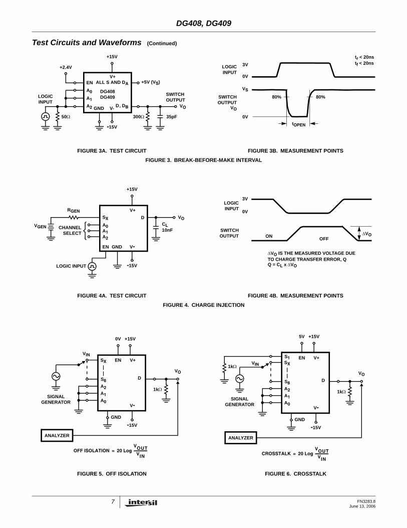
Die CharacteristicsDIE DIMENSIONS:
1800µm x 3320µm x 485µm
METALLIZATION:Type: SiAlThickness: 12kÅ ±1kÅ
PASSIVATION:Type: NitrideThickness: 8kÅ ±1kÅ
WORST CASE CURRENT DENSITY:9.1 x 10⁴ A/cm2
Metallization Mask LayoutDG408
EN A0 A1 A2 GND(2) (1) (16) (15) (14)
V- (3)
S1 (4)
S2 (5)
S3 (6)
S4 (7)
D(8)
S8
(9)S7
(10)
NC
(13) V+
(12) S5
(11) S6
NC
13 FN3283.8June 13, 2006
DG408, DG409
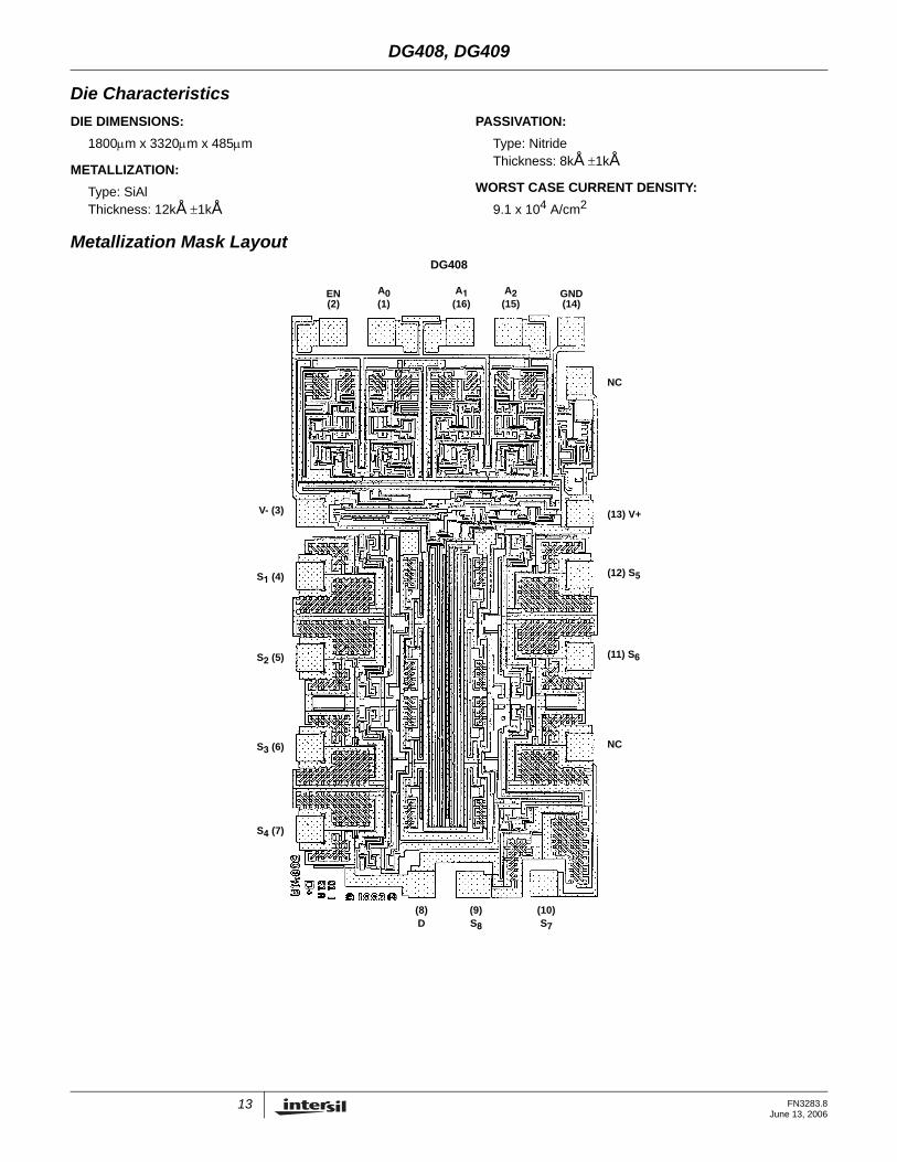
Die CharacteristicsDIE DIMENSIONS:
1800µm x 3320µm x 485µm
METALLIZATION:Type: SiAlThickness: 12kÅ ±1kÅ
PASSIVATION:Type: NitrideThickness: 8kÅ ±1kÅ
WORST CASE CURRENT DENSITY:9.1 x 10⁴ A/cm2
Metallization Mask LayoutDG409
EN A0 A1 GND(2) (1) (16) NC (15)
DA(8)
NC
(14) V+
(13) S1B
(12) S2B
(11) S3B
DB(9)
S4B(10)
V- (3)
S1A (4)
S2A (5)
S3A (6)
S4A (7)
14 FN3283.8June 13, 2006

15 FN3283.8June 13, 2006
DG408, DG409
Thin Shrink Small Outline Plastic Packages (TSSOP)
NOTES:
1. These package dimensions are within allowable dimensions of JEDEC MO-153-AB, Issue E.
2. Dimensioning and tolerancing per ANSI Y14.5M-1982.
3. Dimension “D” does not include mold flash, protrusions or gate burrs. Mold flash, protrusion and gate burrs shall not exceed0.15mm (0.006 inch) per side.
4. Dimension “E1” does not include interlead flash or protrusions. Interlead flash and protrusions shall not exceed 0.15mm (0.006inch) per side.
5. The chamfer on the body is optional. If it is not present, a visual index feature must be located within the crosshatched area.
6. “L” is the length of terminal for soldering to a substrate.
7. “N” is the number of terminal positions.
8. Terminal numbers are shown for reference only.
9. Dimension “b” does not include dambar protrusion. Allowable dambar protrusion shall be 0.08mm (0.003 inch) total in excessof “b” dimension at maximum material condition. Minimum spacebetween protrusion and adjacent lead is 0.07mm (0.0027 inch).
10. Controlling dimension: MILLIMETER. Converted inch dimen-sions are not necessarily exact. (Angles in degrees)
α
INDEXAREA
E1
D
N
1 2 3
-B-
0.10(0.004) C AM B S
e
-A-
b
M
-C-
A1
A
SEATING PLANE
0.10(0.004)
c
E 0.25(0.010) BM M
L0.25
0.010
GAUGEPLANE
A2
0.05(0.002)
M16.17316 LEAD THIN SHRINK SMALL OUTLINE PLASTIC PACKAGE
SYMBOL
INCHES MILLIMETERS
NOTESMIN MAX MIN MAX
A - 0.043 - 1.10 -
A1 0.002 0.006 0.05 0.15 -
A2 0.033 0.037 0.85 0.95 -
b 0.0075 0.012 0.19 0.30 9
c 0.0035 0.008 0.09 0.20 -
D 0.193 0.201 4.90 5.10 3
E1 0.169 0.177 4.30 4.50 4
e 0.026 BSC 0.65 BSC -
E 0.246 0.256 6.25 6.50 -
L 0.020 0.028 0.50 0.70 6
N 16 16 7
α 0o 8o 0o 8o -
Rev. 1 2/02

16 FN3283.8June 13, 2006
DG408, DG409
Dual-In-Line Plastic Packages (PDIP)
NOTES:1. Controlling Dimensions: INCH. In case of conflict between English and
Metric dimensions, the inch dimensions control.2. Dimensioning and tolerancing per ANSI Y14.5M-1982.3. Symbols are defined in the “MO Series Symbol List” in Section 2.2 of
Publication No. 95.4. Dimensions A, A1 and L are measured with the package seated in JE-
DEC seating plane gauge GS-3.5. D, D1, and E1 dimensions do not include mold flash or protrusions.
Mold flash or protrusions shall not exceed 0.010 inch (0.25mm).6. E and are measured with the leads constrained to be perpendic-
ular to datum .7. eB and eC are measured at the lead tips with the leads unconstrained.
eC must be zero or greater.8. B1 maximum dimensions do not include dambar protrusions. Dambar
protrusions shall not exceed 0.010 inch (0.25mm).9. N is the maximum number of terminal positions.
10. Corner leads (1, N, N/2 and N/2 + 1) for E8.3, E16.3, E18.3, E28.3, E42.6 will have a B1 dimension of 0.030 - 0.045 inch (0.76 - 1.14mm).
eA-C-
CL
E
eA
CeB
eC
-B-
E1INDEX 1 2 3 N/2
N
AREA
SEATING
BASEPLANE
PLANE
-C-
D1
B1B
e
D
D1
AA2
L
A1
-A-
0.010 (0.25) C AM B S
E16.3 (JEDEC MS-001-BB ISSUE D)16 LEAD DUAL-IN-LINE PLASTIC PACKAGE
SYMBOL
INCHES MILLIMETERS
NOTESMIN MAX MIN MAX
A - 0.210 - 5.33 4
A1 0.015 - 0.39 - 4
A2 0.115 0.195 2.93 4.95 -
B 0.014 0.022 0.356 0.558 -
B1 0.045 0.070 1.15 1.77 8, 10
C 0.008 0.014 0.204 0.355 -
D 0.735 0.775 18.66 19.68 5
D1 0.005 - 0.13 - 5
E 0.300 0.325 7.62 8.25 6
E1 0.240 0.280 6.10 7.11 5
e 0.100 BSC 2.54 BSC -
eA 0.300 BSC 7.62 BSC 6
eB - 0.430 - 10.92 7
L 0.115 0.150 2.93 3.81 4
N 16 16 9
Rev. 0 12/93
17
All Intersil U.S. products are manufactured, assembled and tested utilizing ISO9000 quality systems.Intersil Corporation’s quality certifications can be viewed at www.intersil.com/design/quality
Intersil products are sold by description only. Intersil Corporation reserves the right to make changes in circuit design, software and/or specifications at any time withoutnotice. Accordingly, the reader is cautioned to verify that data sheets are current before placing orders. Information furnished by Intersil is believed to be accurate andreliable. However, no responsibility is assumed by Intersil or its subsidiaries for its use; nor for any infringements of patents or other rights of third parties which may resultfrom its use. No license is granted by implication or otherwise under any patent or patent rights of Intersil or its subsidiaries.
For information regarding Intersil Corporation and its products, see www.intersil.com
FN3283.8June 13, 2006
DG408, DG409
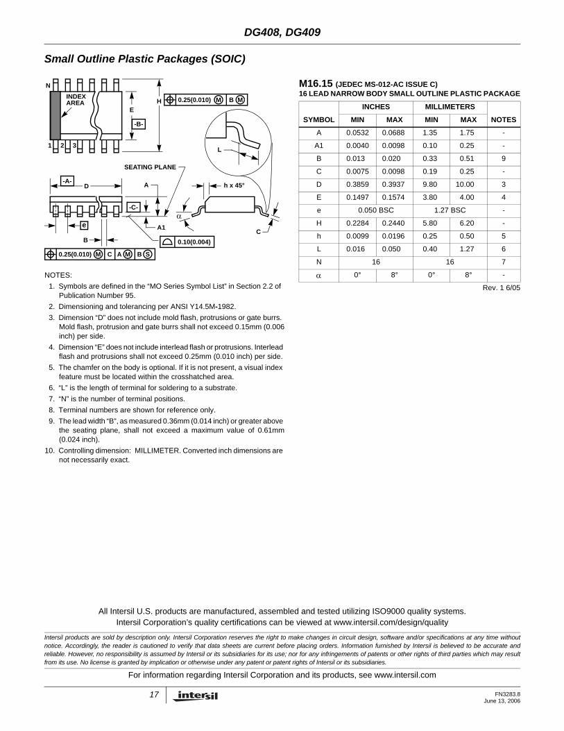
Small Outline Plastic Packages (SOIC)
NOTES:1. Symbols are defined in the “MO Series Symbol List” in Section 2.2 of
Publication Number 95.2. Dimensioning and tolerancing per ANSI Y14.5M-1982.3. Dimension “D” does not include mold flash, protrusions or gate burrs.
Mold flash, protrusion and gate burrs shall not exceed 0.15mm (0.006inch) per side.
4. Dimension “E” does not include interlead flash or protrusions. Interlead flash and protrusions shall not exceed 0.25mm (0.010 inch) per side.
5. The chamfer on the body is optional. If it is not present, a visual index feature must be located within the crosshatched area.
6. “L” is the length of terminal for soldering to a substrate.7. “N” is the number of terminal positions.8. Terminal numbers are shown for reference only.9. The lead width “B”, as measured 0.36mm (0.014 inch) or greater above
the seating plane, shall not exceed a maximum value of 0.61mm(0.024 inch).
10. Controlling dimension: MILLIMETER. Converted inch dimensions are not necessarily exact.
INDEXAREA
E
D
N
1 2 3
-B-
0.25(0.010) C AM B S
e
-A-
L
B
M
-C-
A1
A
SEATING PLANE
0.10(0.004)
h x 45°
C
H 0.25(0.010) BM M
α
M16.15 (JEDEC MS-012-AC ISSUE C)16 LEAD NARROW BODY SMALL OUTLINE PLASTIC PACKAGE
SYMBOL
INCHES MILLIMETERS
NOTESMIN MAX MIN MAX
A 0.0532 0.0688 1.35 1.75 -
A1 0.0040 0.0098 0.10 0.25 -
B 0.013 0.020 0.33 0.51 9
C 0.0075 0.0098 0.19 0.25 -
D 0.3859 0.3937 9.80 10.00 3
E 0.1497 0.1574 3.80 4.00 4
e 0.050 BSC 1.27 BSC -
H 0.2284 0.2440 5.80 6.20 -
h 0.0099 0.0196 0.25 0.50 5
L 0.016 0.050 0.40 1.27 6
N 16 16 7
α 0° 8° 0° 8° -
Rev. 1 6/05